ruggedized architecture design guide - advantechadvcloudfiles.advantech.com/rtx-standard/doc/rtx...
TRANSCRIPT

Ruggedized Architecture Design Guide
Version 1.0 Dec., 2015

2
REVISION HISTORY
Rev Date Notes
0.1 Sep 18, 2014 Initial release
1.0 Dec 30, 2015 First version

3
Contents
1. Introduction .................................................................................................................... 10
1.1 General Introduction ...................................................................................... 10
1.2 Purpose of This Document ............................................................................ 11
1.3 Design Support .............................................................................................. 11
1.4 Abbreviations and Acronyms Used ............................................................... 11
1.5 Reference Document ..................................................................................... 14
1.5.1 RTX 2.0 Specification V2.0, Nov, 2015. ........................................................ 14
1.5.2 Industry Standards Documents ..................................................................... 14
1.6 Schematic Example Correctness .................................................................. 15
1.7 Software Support ........................................................................................... 15
1.8 Schematic Example Conventions (TBD) ....................................................... 16
2. Infrastructure: Connector, Power Delivery, System Management ........................... 17
2.1 Module Connector ......................................................................................... 17
2.2 Module Power ................................................................................................ 20
2.2.1 Input Voltage Range ...................................................................................... 20
2.2.2 Input Voltage Rise Time ................................................................................ 20
2.2.3 Module Maximum Input Power ...................................................................... 21
2.2.4 Power Path .................................................................................................... 21
2.3 Module I/O Power .......................................................................................... 22
2.4 RTX_PGOOD and CB_PGOOD ................................................................... 23
2.5 CB_PWR_EN ................................................................................................ 23
2.6 RESET IN Module ......................................................................................... 24
2.7 Power Button ................................................................................................. 24
2.8 Power up Sequence ...................................................................................... 24
2.9 Boot Selection ............................................................................................... 25
2.9.1 Boot Definitions ............................................................................................. 25
4
2.9.2 RTX BOOT_SEL Pins ................................................................................... 26
2.10 RTC Backup Power ....................................................................................... 26
3. Display Interfaces .......................................................................................................... 27
3.1 Module LVDS ................................................................................................ 27
3.1.1 Display – 18/24 bits LVDS LCD Single Channel ........................................... 27
3.1.2 Display Parameter and EDID ........................................................................ 30
3.1.3 Power Sequence of LVDS Panel Requirement ............................................. 30
3.1.4 Power Delivery of LVDS panel ...................................................................... 30
3.2 Embedded DisplayPort (eDP) Display .......................................................... 31
3.2.1 eDP interface ................................................................................................. 31
3.2.2 eDP/LVDS LCD Pin Sharing ......................................................................... 31
3.3 HDMI .............................................................................................................. 32
3.4 Parallel LCD .................................................................................................. 33
3.5 VGA ............................................................................................................... 33
4. Low/Medium Speed Serial I/O Power Interfaces ........................................................ 34
4.1 Asynchronous Serial Ports ............................................................................ 34
4.1.1 RS232 Ports .................................................................................................. 34
4.1.2 RS485 Half-Duplex ........................................................................................ 35
4.1.3 RS422 Half-Duplex ........................................................................................ 35
4.2 I2C Interfaces ................................................................................................ 35
4.2.1 General .......................................................................................................... 36
4.2.2 I2C Level Transition, Isolation and Buffering................................................. 36
4.2.3 I2C_PM Bus EEPROMs ................................................................................ 37
4.2.4 General I2C Bus EEPROMs.......................................................................... 37
4.2.5 I2C Based IO Expanders ............................................................................... 37
4.3 I2S Interfaces ................................................................................................ 38
4.3.1 General .......................................................................................................... 38

5
4.3.2 Freescale SGTL5000 I2S Audio Example ..................................................... 38
4.3.3 Intel High Definition Audio Over I2S2 ............................................................ 39
4.4 4.4 SPI Interface ............................................................................................ 40
4.4.1 General .......................................................................................................... 40
4.4.2 RTX Implementation ...................................................................................... 40
4.5 CAN Bus ........................................................................................................ 40
4.5.1 General .......................................................................................................... 40
4.5.2 RTX Implementation ...................................................................................... 41
4.5.3 Isolation ......................................................................................................... 41
5. High Speed Serial I/O Interfaces .................................................................................. 41
5.1 USB Bus ........................................................................................................ 41
5.1.1 General .......................................................................................................... 41
5.1.2 USB OTG....................................................................................................... 42
5.1.3 USB 2.0/USB 3.0 Host Ports ......................................................................... 43
5.2 GBE ............................................................................................................... 43
5.2.1 GBE Carrier Connector Implementation Example ........................................ 43
5.2.2 GBE Mag-Jack Connector Recommendation ............................................... 44
5.2.3 GBE LEDs ..................................................................................................... 45
5.3 PCIe ............................................................................................................... 46
5.3.1 General .......................................................................................................... 46
5.3.2 PCIe X1 add-in Card on Carrier .................................................................... 46
5.3.3 PCIe M.2 (TBD) ............................................................................................. 46
5.4 SATA ............................................................................................................. 47
5.4.1 General .......................................................................................................... 47
5.4.2 SATA Form Factor ......................................................................................... 47
5.4.3 SATA-DOM .................................................................................................... 48
5.4.4 SATA Connector ............................................................................................ 48

6
6. Memory Card Interfaces ................................................................................................ 49
6.1 SD Card ......................................................................................................... 49
6.2 eMMC ............................................................................................................ 50
7. Camera Interfaces.......................................................................................................... 51
7.1 General .......................................................................................................... 51
7.2 Camera Data Interface formats ..................................................................... 52
7.3 Serial Camera Interface Example ................................................................. 52
7.4 Parallel Camera Interface Example ............................................................... 53
7.5 CSI/PCAM Pin Sharing .................................................................................. 54
8. GPIO ................................................................................................................................ 55
8.1 RTX Module GPIO ......................................................................................... 55
8.2 RTX GPIO multi-function Pin Sharing for Keypad ......................................... 55
9. System Bus Interface .................................................................................................... 56
9.1 General .......................................................................................................... 56
9.2 Support .......................................................................................................... 56
10. Thermal Design and Management ............................................................................... 56
10.1 General .......................................................................................................... 56
10.2 Heat Spreader ............................................................................................... 56
10.3 Thermal Resistance Calculations .................................................................. 57
11. Carrier Board PCB Design Overview ........................................................................... 58
11.1 General PCB Stack-up and consideration ..................................................... 58
11.2 Six Layers PCB Stack-up .............................................................................. 58
11.3 Trace Parameters for High Speed Differential Interface ............................... 59
11.4 Trace Parameters for High Single Ended Interface (TBD) ............................ 59
7
Figure Figure 1 Schematic Symbol Conventions ............................................................................... 16
Figure 2 Connector Pins A1 to A100 ....................................................................................... 17
Figure 3 Connector Pins B1 to B100 ....................................................................................... 18
Figure 4 Connector Pins C1 to C100....................................................................................... 19
Figure 5 Connector Pins D1 to D100....................................................................................... 20
Figure 6 Soft-Start Circuit on Power Rail ................................................................................ 21
Figure 7 Basic Module and Carrier Power Path ...................................................................... 22
Figure 8 MOSFET Level Shift .................................................................................................. 23
Figure 9 VGA DDC signal level shift pass gate circuit ............................................................ 23
Figure 10 Reset Button ............................................................................................................ 24
Figure 11 Power Button ........................................................................................................... 24
Figure 12 Power up Sequence ................................................................................................ 25
Figure 13 BOOT Select Function ............................................................................................ 26
Figure 14 RTC and CMOS Circuit ........................................................................................... 26
Figure 15 LVDS Interface ........................................................................................................ 27
Figure 16 LED Backlight Voltage Selection ............................................................................. 28
Figure 17 Panel LED Voltage Control and Brightness Control ............................................... 29
Figure 18 Power Sequence of LVDS panel ............................................................................. 30
Figure 19 HDMI Interface ........................................................................................................ 33
Figure 20 Parallel LCD Interface to VGA interface .................................................................. 34
Figure 21 RS232...................................................................................................................... 34
Figure 22 RS485...................................................................................................................... 35
Figure 23 RS422...................................................................................................................... 35
Figure 24 I2C Level Shift ......................................................................................................... 36
Figure 25 EEPROM I2C .......................................................................................................... 37
Figure 26 I2C IO Expanders .................................................................................................... 38
8
Figure 27 Freescale I2S Audio ................................................................................................ 38
Figure 28 Daughter board for Intel HD Audio .......................................................................... 39
Figure 29 SPI ROM ................................................................................................................. 40
Figure 30 CAN Bus Transceiver .............................................................................................. 41
Figure 31 USB 2.0 OTG .......................................................................................................... 42
Figure 32 USB 3.0 IO .............................................................................................................. 43
Figure 33 GBE Application ...................................................................................................... 44
Figure 34 PCIe X1 ................................................................................................................... 46
Figure 35 SATA-DOM ............................................................................................................. 48
Figure 36 SATA Connector ..................................................................................................... 48
Figure 37 SD Card ................................................................................................................... 49
Figure 38 eMMC ...................................................................................................................... 50
Figure 39 CSI Module .............................................................................................................. 52
Figure 40 Parallel Camera Module .......................................................................................... 53
Figure 41 Keypad .................................................................................................................... 55
Figure 42 Heat Spreader 2D Drawing ..................................................................................... 56
Figure 43 Z-Height of Carrier board and Module with Heat Spreader .................................... 56
Figure 44 SIX Layers PCB Stack-Up Example of 1.6mm (62 mils) Thick PCB ...................... 58

9
Table Table 1 Schematic Power Naming .......................................................................................... 17
Table 2 BOOT Device Selection .............................................................................................. 26
Table 3 LVDS/eDP Pin Assignment ........................................................................................ 31
Table 4 Magnetics Characterstics ........................................................................................... 45
Table 5 SATA Form Factor ...................................................................................................... 47
Table 6 CSI/PACM Pin Assignment ........................................................................................ 54
Table 7 GPIO Multi-function Pin Assignment .......................................................................... 55
Table 8 Thermal Table ............................................................................................................ 57
Table 9 Impedance Table and Trace Width/Spacing of 1.6mm (62 mils) Thick PCB ............. 59

10
1. Introduction
1.1 General Introduction The RTX 2.0 (Ruggedized Technology eXtended) specification is a Ruggedized Standard
platform designed for demanding applications. Through its innovative mechanical and
electrical design, products designed with RTX2.0 can perform in complex and challenging
environments such as military, logistics, transportation/fleet management, and many other
industrial applications.
RTX 2.0-based modules include four board-to-board connectors for all I/O signals and
mounting hole locations. The asymmetrical mounting hole design provides two advantages.
Firstly, they provide an effective fool-proof solution during assembly. Secondly, the defined
mounting holes not only allow screw fixing onto the carrier board via metal nuts, but also
provide superior heat dispersion. As for I/O expansion, RTX 2.0 uses the standard 400-pin
definition through four connectors providing customers with high I/O expandability. Also, it
takes the latest interface trends into account. RTX 2.0 supports both USB 3.0 and MIPI/CSI-2
(Camera interface) to offer better expansion that can meet a variety of different requirements.
Applications included:
Military
Industrial control system
Transportation/Fleet management
Robotic
Power equipment
Inspection equipment
11
1.2 Purpose of This Document This document provides design recommendations for an RTX 2.0 Carrier Board, which is
based on an RTX 2.0 Module. It identifies the hardware integration aspect that must be
considered when designing a platform or application.
The document is written for system hardware engineers. It also addresses firmware and
OS/Software implications wherever applicable. This guide is intended to aid hardware
designers, to help them understand the application of the modules they are developing and
RTX infrastructure.
Note: The document provides signal routing trace length on the board level only and excludes
package length information.
Note: This document is based on the existing industry specification, which may be revised and
upgraded. All information specified is preliminary based on current expectations, and are
subject to change without notice.
1.3 Design Support There are a number of ways to have a RTX 2.0 Carrier board developed:
Consult with your RTX 2.0 module vendor to review your design or follow their
design checklist. Make sure to also have the appropriate semiconductor
companies review the portions of the design that utilize their components, or
follows up their design applications and design guideline.
Use a 3rd party firm that specializes in RTX 2.0 Carrier Board development.
Contact your RTX 2.0 module vendor. The module vendor may have an FAE
available for advice. Many vendors may undertake custom carrier board design
projects for significant opportunities.
1.4 Abbreviations and Acronyms Used ADC Analog to Digital Converter
ARM Advanced RISC Machines www.arm.com
BCT Boot Configuration Table
BSP (Software) Board Support Package
CAD Computer Aided Design
CAN Controller Area Network
CPLD Complex Programmable Logic Device
CODEC Coder – Decoder
CSI Camera Serial Interface www.mipi.org

12
DAC Digital to Analog Converter
DB-9 Connector, D shaped, B shell size, 9 pins
DE Differential Ended (signal pair)
DNI Do Not Install (component is not loaded)
DSP Digital Signal Processor
EDID Extended Display Identification Data www.vesa.org
EEPROM Electrically Erasable Programmable Read Only Memory
eMMC Embedded Multi Media Card www.jedec.org
ESD Electro Static Discharge
FET Field Effect Transistor
FIFO First In First Out (buffer memory)
FS Full Speed (USB 2.0 12 Mbps)
GBE Gigabit Ethernet www.ieee.org
Gbps Giga bits per second
GPIO General Purpose Input / Output
HDA High Definition Audio – Intel defined format www.intel.com
HDMI High Definition Multimedia Interface www.hdmi.org
HID Human Interface Device: USB device class
HS High Speed (USB 2.0 480 Mbps)
IC Integrated Circuit
I2C Inter-Integrated Circuit www.nxp.com
I2S Inter-Integrated Circuit – Sound www.nxp.com
IEEE Institute of Electrical and Electronics Engineers www.ieee.org
iMX6 Popular ARM SOC from Freescale Semiconductor www.freescale.com
IO Input Output
ISO International Organization for Standardization (French) www.iso.org
JEDEC Joint Electron Device Engineering Council www.jedec.org
JPEG Joint Photographic Experts Group www.jpeg.org
LED Light Emitting Diode
LVDS Low Voltage Differential Signaling
M2.5 Metric 2.5mm
M3 Metric 3.0mm
MAC Media Access Controller (e.g. logic circuits in GBE)
Mbps Mega bits per second
MIPI Mobile Industry Processor Interface www.mipi.org
MLC Multi Level Cell (Flash Memory Reference)

13
MO-297 Module Outline 297 (“Slim SATA” format) www.jedec.org
MO-300 Module Outline 300 (mini-PCIe Express card format) www.jedec.org
MPEG Motion Picture Experts Group www.mpeg.org
NAND A high density flash memory technology
nS Nano second (10 E -9)
NC Not Connected
NXP A semiconductor company www.nxp.com
OS Operating System
OTG On the Go (USB term – device can be host or client)
PCB Printed Circuit Board
PHY Physical (transceiver) – drives cable
PICMG PCI Industrial Computer Manufacturing Group www.picmg.org
PCI Peripheral Component Interface www.pcisig.org
PCIe PCI Express www.pcisig.org
PCI-SIG PCI Special Interest Group www.pcisig.org
PCM Pulse-Code Modulation
PLL Phase Locked Loop
POE Power Over Ethernet
pS Pico second (10 E -12)
PWM Pulse Width Modulation
RGB Video data in Red Green Blue pixel format
RISC Reduced Instruction Set Computing
ROM Read Only Memory
RS232 Recommend Standard 232 (asynch serial ports)
RS485 Asynchronous serial data, differential, multi drop
RTC Real Time Clock (battery backed clock and memory)
SAR Successive Approximation Register
SATA Serial ATA (serial mass storage interface) www.sata-io.org
SD Secure Digital (memory card)
SE Single Ended (signal, as opposed to differential)
SLC Single Level Cell (flash memory reference)
SMSC A semiconductor company www.smsc.com
SOC System On Chip
S/PDIF Sony/Philips Digital Interconnect Format
SPI Serial Peripheral Interface
SSD Solid State Disk

14
TI Texas Instruments – semiconductor company www.ti.com
TIM Thermal Interface Material
UART Universal Asynchronous Receiver Transmitter
UL Underwriters Laboratories www.ul.com
USB Universal Serial Bus www.usb.org
VESA Video Electronics Standards Association www.vesa.org
WEC7 Windows Embedded Compact 7 (an OS)
YUV Video data format, more common in television
X5R Ceramic capacitor dielectric – Capactiance tolerance +-10% and Operation
temperature -55C~85C
X7R Ceramic capacitor dielectric – Capactiance tolerance +-10% and Operation
temperature -55C~125C
X86 Intel architecture (80x86) CPUs
1.5 Reference Document 1.5.1 RTX 2.0 Specification V2.0, Nov, 2015.
1.5.2 Industry Standards Documents
PICMG® EEEP Embedded EEPROM Specification, Rev. 1.0, August 2010
(www.picmg.org). PCI Express Specifications (www.pci-sig.org).
PCI Express Mini Card Electromechanical Specification Revision 2.0, April 21, 2012,
© PCI-SIG (www.pci-sig.org).
PCI Express M.2 Specification V1.0, Nov. 01, 2013, © PCI-SIG (www.pci-sig.org).
eMMC (“Embedded Multi-Media Card”) the eMMC electrical standard is defined by
JEDEC JESD84-B51 and the mechanical standard by JESD84-C44 (www.jedec.org).
SD Specifications Part 1 Physical Layer Simplified Specification, Version4.01, Jan
22, 2013, © 2010 SD Group and SD Card Association (“Secure Digital”)
(www.sdcard.org).
GBE MDI (“Gigabit Ethernet Medium Dependent Interface”) defined by IEEE 802.3.
The 1000Base-T operation over copper twisted pair cabling defined by IEEE 802.3ab
(www.ieee.org).
CAN (“Controller Area Network”) Bus Standards – ISO 11898, ISO 11992, SAE
J2411.
CSI-2 (Camera Serial Interface version 2) The CSI-2 standard is owned and
maintained by the MIPI Alliance (“Mobile Industry Processor Interface Alliance”)
(www.mipi.org).
HDMI Specification, Version 1.3a, November 10, 2006 © Hitachi and other companies

15
(www.hdmi.org).
The I2C Specification, Version V6, April 04 2014, Philips Semiconductor (now NXP)
(www.nxp.com).
I2S Bus Specification, Feb. 1986 and Revised June 5, 1996, Philips Semiconductor
(now NXP) (www.nxp.com).
JEDEC MO-300 (mSATA) defines the physical form factor of the mSATA format
(www.jedec.org). The electrical connections are defined in the Serial ATA document.
RS-232 (EIA “Recommended Standard 232”) this standard for asynchronous serial port
data exchange dates from 1962. The original standard is hard to find. Many good
descriptions of the standard can be found on-line, e.g. at Wikipedia, and in text books.
Serial ATA Revision 3.1, July 18, 2011, Gold Revision, © Serial ATA International
Organization (www.sata-io.org).
SPDIF (aka S/PDIF) (“Sony Philips Digital Interconnect Format) - IEC 60958-3.
SPI Bus – “Serial Peripheral Interface” – de-facto serial interface standard defined by
Motorola. A good description may be found on Wikipedia
(http://en.wikipedia.org/wiki/Serial_Peripheral_Interface_Bus).
SMARC Specification Ver 1.1, Feb. 21, 2013
SMARC Design Guide Ver 1.0, Aug. 26 2013
USB Specifications (www.usb.org).
VESA Enhanced Extended Display Identification Data Standard, Rev. 1, Feb 9, 2000,
VESA (www.vesa.org) See also the “EDID” page in Wikipedia.
1.6 Schematic Example Correctness The schematic examples shown in this Design Guide are implemented to be working correctly-
although correctness can’t be guaranteed for all applications. Most of the examples have been
applied to the Demo Carrier Board that has been built, tested, and are verified to work.
1.7 Software Support Hardware examples and suggestions are given in the following pages. RTX 2.0 Carrier
hardware design should consider software driver support as part of your checklist. Windows
Embedded driver web checklist is as below. It is one of methods to check out driver support on
Windows Embedded OS platforms.
http://www.microsoft.com/windowsembedded/en-us/drivercatalog.aspx
Regarding Linux, please consult with your IC vender, OS vender, OS community, and your
module vender for driver support and maintenance. In addition, you can write your own driver

16
as well. Most RTX module vendors offer a BSP (Board Support Package) to support module
SOC for each interface driver. Please review the BSP and the device drivers included in your
HW device to avoid software development delays.
1.8 Schematic Example Conventions Some of the conventions used in the examples are described below. The symbol of Off-page
has a number index to connect to the schematic page.
Figure 1 Schematic Symbol Conventions

17
Table 1 Schematic Power Naming
+ADP_MAIN Power source to the overall system. Before DCDC converter
with UVP and OVP protection circuit.
+VDD_RTX Main power to RTX module. Voltage range is from 5V to 24V.
+V3A 3.3V standby power.
+VDD_RTC RTC backup power to RTX module. Combine with +V3A and
coin battery.
+V3 3.3V IO power supply.
+V5 5V IO power supply.
+V12 12V IO power supply.
2. Infrastructure: Connector, Power Delivery, System
Management
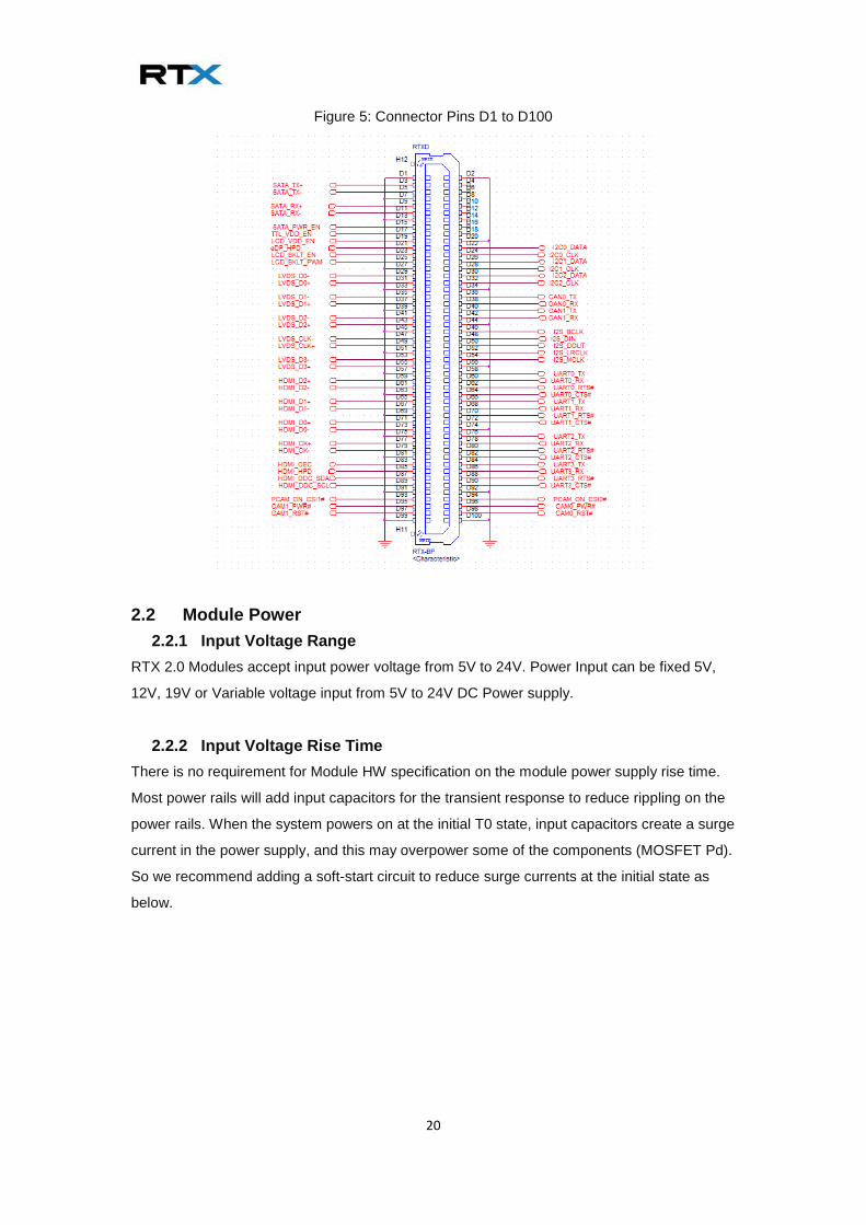
2.1 Module Connector The RTX 2.0 Module Connector is well described in The RTX 2.0 Specification and the
complete description is not repeated here. RTX 2.0 Module connector is a low profile of board
to board connector. There are 4 pairs of 100 pins so each connector has 400 pins. The option
mating height of the connector is 3mm or 5mm depending on the system design.
Various height profiles are available for the RTX 2.0 Module connector. The lowest profile
available has a Carrier Board PCB top-side to Module PCB bottom-side separation of 2.5mm,
and connector mating height of 3mm.
Figure 2: Connector Pins A1 to A100

18
Figure 3: Connector Pins B1 to B100

19
Figure 4: Connector Pins C1 to C100
20
Figure 5: Connector Pins D1 to D100
2.2 Module Power 2.2.1 Input Voltage Range
RTX 2.0 Modules accept input power voltage from 5V to 24V. Power Input can be fixed 5V,
12V, 19V or Variable voltage input from 5V to 24V DC Power supply.
2.2.2 Input Voltage Rise Time
There is no requirement for Module HW specification on the module power supply rise time.
Most power rails will add input capacitors for the transient response to reduce rippling on the
power rails. When the system powers on at the initial T0 state, input capacitors create a surge
current in the power supply, and this may overpower some of the components (MOSFET Pd).
So we recommend adding a soft-start circuit to reduce surge currents at the initial state as
below.

21
Figure 6: Soft-Start Circuit on Power rail
2.2.3 Module Maximum Input Power
The RTX 2.0 specification document states that the input voltage range is 5.0V to 24V. Each
RTX 2.0 connector pin is able to carry 0.5A current maximum. The RTX module allocates 12
pins for input power and 89 pins for ground. Allow 6A max at +5.0V with 30W or allow 2.5A at
fixed 12V with 30 watts. You may consider derating the wattage to 80% and the maximum
input power 24 watt. For instance, Freescale dual core SOC is rated at 6 watt and RTX 2.0
input power still has room to upgrade SOC performance to Qual-core and trade off the total
power budget.
2.2.4 Power Path
The power path for a basic input voltage and DC converter arrangement for RTX 2.0 carrier
board is shown in Figure 7. The figure also shows carrier board power supply sections
assuming a typical system powered by power source fixed at 19V. However, you may design a
variable source in the 5V to 24V range.

22
Figure 7: Basic Module and Carrier Power Path
2.3 Module I/O Power RTX 2.0 only supports 3.3V I/O except USB_OTG_VBUS_DET is 5V. HDMI control (DCC)
signals and VGA control (DCC) are 3.3V I/O on module. HDMI control (DDC) signals and VGA
control (DDC) signals are 5V at sink (Devices) and have a level shift between +3V and +5V.
The recommendation for the gate circuit is as below (IC level shift is acceptable, but the cost is
higher.)
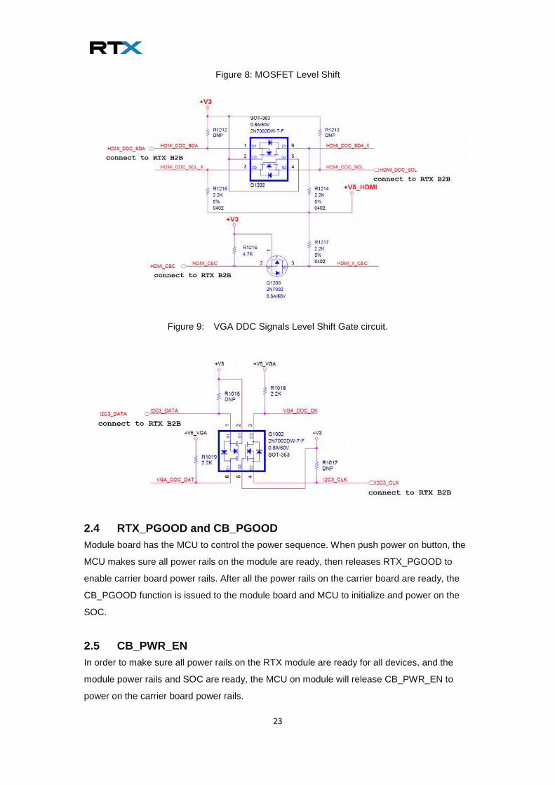
23
Figure 8: MOSFET Level Shift
Figure 9: VGA DDC Signals Level Shift Gate circuit.
2.4 RTX_PGOOD and CB_PGOOD Module board has the MCU to control the power sequence. When push power on button, the
MCU makes sure all power rails on the module are ready, then releases RTX_PGOOD to
enable carrier board power rails. After all the power rails on the carrier board are ready, the
CB_PGOOD function is issued to the module board and MCU to initialize and power on the
SOC.
2.5 CB_PWR_EN In order to make sure all power rails on the RTX module are ready for all devices, and the
module power rails and SOC are ready, the MCU on module will release CB_PWR_EN to
power on the carrier board power rails.

24
2.6 RESET_IN Module The RTX RESET_IN# signal may be used to force a RTX system reset. It is an input to the
module that pulls up resistance on the module. If implemented by the carrier board, request an
open drain circuit or a switch to GND should be used. An example is show below.
Figure: 10: Reset Button
2.7 Power Button RTX not only defines a pin to allow the implementation of a carrier board power button, but
also uses the MCU to control the power sequence on the module board and carrier board to
make sure power rails are consistent. Please refer to the 2.8 Power up Sequence diagram.
Figure 11: Power Button
2.8 Power up Sequence

25
Figure 12: Power up Sequence
2.9 Boot Selection
2.9.1 Boot Definitions
Most SOC used on RTX Modules have the following attributes.
Step 1: SOC has an internal ROM. The internal ROM code is executed after the SOC is reset.
This ROM code is provided by the silicon vendor and is inside the SOC.
Step 2: A set of SOC strap pins are used to option what SOC physical device interfaces (SATA,
SD Card, SPI, eMMC, etc.) will be used for the Step 2 boot process.
Step 3: The SOC pin configuration is very flexible that most of the SOC pins can be used for
several functions, and the RTX Module designer must choose a pin configuration that works
for the design configuration. The SOC pin configuration is set by a Boot Configuration Table
that is read from external boot media (SATA, SD Card, SPI, eMMC, etc).
There are 3 steps in the boot process:
Step 1: Internal SOC ROM execution
Step 2: Boot from non-volatile memory external to the SOC: BCT is loaded and various other
system parameters are configured
Step 3: Operating System Loading
The Operating System load may occur from the same memory as Step 2 BCT boot, or step 2

26
code may pass the Operating System loading from other devices like USB drive or SATA
drive.
2.9.2 RTX BOOT_SEL Pins
RTX 2.0 HW specification defines 3 GPIO pins as optional Boot Sources from BOOT_SEL0#
to BOOT_SEL2#. They can be used to inform the module what boot device to BCT boot from.
The table below is a BOOT source and BOOT_SEL mapping and reference circuit table for the
carrier board.
Table 2: BOOT Device Selection
Carrier Connection Boot Source
BOOT_SEL2# BOOT_SEL1# BOOT_SEL0#
0 GND GND GND Carrier SATA
1 GND GND Float Carrier SD Card
2 GND Float GND Carrier eMMC Flash
3 GND Float Float Carrier SPI
4 Float GND GND Module device (NAND, NOR) –
vendor specific
5 Float GND Float Remote boot (GBE, serial) –
vendor specific
6 Float Float GND Module eMMC
7 Float Float Float Module SPI
Figure 13: BOOT Select Function
2.10 RTC Backup Power The MCU module to control power on sequence needs to be always powered to enable I2C on
MCU.
Figure 14: RTC and CMOS circuit

27
3. Display Interfaces
3.1 Module LVDS 3.1.1 Display – 18/24 bits LVDS LCD Single Channel
The LVDS interface module is used with single channel LVDS displays 18/24bits. Typically
supporting LVDS 18-bit single channel operation (3 data pairs plus one clock pair) and
supporting LVDS 24-bit single channel operation (4 data pairs plus one clock pair). Please
refer to your LCD panel vender spec to define your LVDS cable. The LVDS interface uses
differential signals and impedance is 100 ohms. We recommend using coax type cables to
control impedance matching to meet with the signal integrity spec. Add grounding pins next to
the LVDS differential pair with current loop and EMC performance.
Figure 15: LVDS interface

28
Reserve Display LED backlight has 5V and 12V options via jumper setting.
Figure 16: LED Backlight Voltage Selections

29
There are two backlight control signals: PANEL_BKLT_EN and PANEL_BKLT_PWM.
PANEL_BKLT_EN enables backlight power rail for LED inside panel. PANEL_BKLT_PWM
allows modulation PWM frequency to change the voltage for LED brightness. Some designs
require a separate LVDS and backlight interface; depending on your product spec and
application.
Figure 17: Panel LED Voltage Control and Brightness Control

30
3.1.2 Display Parameter and EDID
The E-EDID Standard defines requirements and options for data structures that enable a
display (Sink) to inform the host (Source) about its identity and capabilities. This standard also
makes recommendations for some data fields. Host (Source) devices are required to read and
properly handle the data that a display (Sink) provides. The EDID data structure is
independent of the communications protocol used between the display (Sink) and the host
(Source). Enhanced EDID defines a basic data structure (known as BASE EDID or block 0) of
128 bytes that all compliant displays shall supply. E-EDID also defines the rules for how
EXTENSIONS may be added to the BASE structure.
EDID of I2C on Module is 3.3V. If your panel spec of EDID interface is 5V, please add level
shift from 5V to 3.3V.
3.1.3 Power Sequence of LVDS Panel Requirement
Figure 18: Power Sequence of LVDS Panel.
Figure 18 is about the LCD panel power sequence, each vender may define it slightly
differently. Please refer to each specific panel specification that you implement in your system
and work with SW team to fine tune it.
3.1.4 Power Delivery of LVDS panel
The carrier board provides the power supply for flat panels. The power delivery path from the
carrier board to panel may have variable DC resistance to cause voltage drops and panel
display issues, so you need to meet the power tolerance on the panel spec for voltage. Most
carrier board designs may add MOSFET to the control power sequence. MOSFET has RDs

31
ON the inside to cause slight voltage drops, PCB and LVDS cables also have similar DC
resistance. Consider the worst case scenarios for power consumption and total DC resistance
on the path to make sure voltage drops meet the panel specification.
3.2 Embedded DisplayPort (eDP) Display 3.2.1 eDP interface
Embedded DisplayPort (eDP) was developed to be used specifically in embedded display
applications. eDP will add new system capabilities while reducing system cost,
power, and size. An eDP cable is recommended and uses mico-coax with a differential
impedance of 85~110 ohms, cable AWG is 40. In the meantime, consider Differential Insertion
Loss, Differential Return Loss, Differential FEXT cables that should include PCB and
connector loss. Most applications of eDP panels are for high resolution 2K or 4K applications.
3.2.2 eDP/LVDS LCD Pin Sharing
eDP interface also shares LVDS interface as in the table below. LVDS interface or eDP
interface are displayed.
Table 3: LVDS / eDP Pin Assignment
Pin
Location
LVDS eDP
D31 LVDS_D0+ EDP_TX0+
D29 LVDS_D0- EDP_TX0-
D37 LVDS_D1+ EDP_TX1+
D35 LVDS_D1- EDP_TX1-
D43 LVDS_D2+ EDP_TX2+
D41 LVDS_D2- EDP_TX2-
D55 LVDS_D3+ EDP_TX3+
D53 LVDS_D3- EDP_TX3-
D49 LVDS_CLK+ EDP_AUX+-
D47 LVDS_CLK- EDP_AUX-
D19 LVDS_VDD_EN EDP VDD_EN
D23 LVDS_BKLT_EN EDP_BKLT_EN
D25 LVDS_BKLT_PWM EDP_BKLT_PWM
D32 I2C2_CLK
(LVDS_I2C_CK)
No use RSVD
D30 I2C2_DATA
(LVDS_I2C_DAT)
No use RSVD
D21 No use EDP_HPD
32
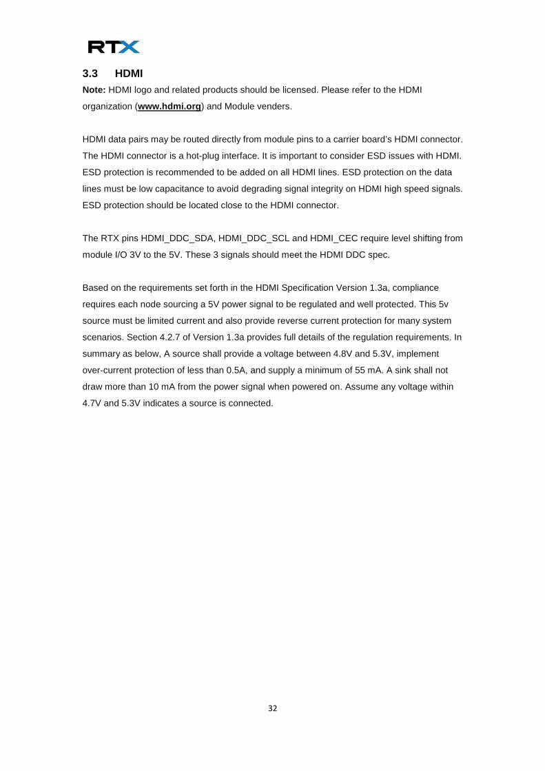
3.3 HDMI Note: HDMI logo and related products should be licensed. Please refer to the HDMI
organization (www.hdmi.org) and Module venders.
HDMI data pairs may be routed directly from module pins to a carrier board’s HDMI connector.
The HDMI connector is a hot-plug interface. It is important to consider ESD issues with HDMI.
ESD protection is recommended to be added on all HDMI lines. ESD protection on the data
lines must be low capacitance to avoid degrading signal integrity on HDMI high speed signals.
ESD protection should be located close to the HDMI connector.
The RTX pins HDMI_DDC_SDA, HDMI_DDC_SCL and HDMI_CEC require level shifting from
module I/O 3V to the 5V. These 3 signals should meet the HDMI DDC spec.
Based on the requirements set forth in the HDMI Specification Version 1.3a, compliance
requires each node sourcing a 5V power signal to be regulated and well protected. This 5v
source must be limited current and also provide reverse current protection for many system
scenarios. Section 4.2.7 of Version 1.3a provides full details of the regulation requirements. In
summary as below, A source shall provide a voltage between 4.8V and 5.3V, implement
over-current protection of less than 0.5A, and supply a minimum of 55 mA. A sink shall not
draw more than 10 mA from the power signal when powered on. Assume any voltage within
4.7V and 5.3V indicates a source is connected.

33
Figure 19: HDMI interface
Discrete circuit may be referred above. The integrated circuit is TI TPD12S016. HW designers
can evaluate which board size and cost they prefer.
3.4 Parallel LCD Refer to the parallel LCD panel spec to fine tune the timing and power up sequence to meet
the LCD specification.
3.5 VGA The RTX 2.0 module does not support VGA interface. Some embedded applications may need
a VGA interface. The alternative is to use a parallel LCD interface to add Triple High Speed
Video DAC (CH7055A) to transfer. The reference circuit is shown below. Please refer to
Chrontel design note and application.

34
Figure 20: Parallel LCD Interface to VGA Interface
4. Low/Medium Speed Serial I/O Power Interfaces 4.1 Asynchronous Serial Ports
4.1.1 RS-232 Ports
The RTX 2.0 module asynchronous serial ports run at 3.3v I/O logic levels. The transmit and
receive data lines from and to the module are active high, and the handshake lines are active
low. If the asynchronous ports are to interface with RS232 level devices, then a carrier RS-232
transceiver is required. The logic side of the transceiver must be able to run at 3.3 I/O levels.
The selection of 3.3v I/O compatible transceivers is a requirement. The Maxim MAX3232,
illustrated in the figures below. The MAX3232 can operate at maximum speeds 1 Mbps. The
transceivers invert the polarity of the incoming and outgoing data and handshake lines.
Figure 21: RS232

35
4.1.2 RS485 Half-Duplex
Figure 22: RS485
4.1.3 RS422 Half-Duplex
Figure 23: RS 422
4.2 I2C Interfaces

36
4.2.1 General
The I2C-bus is a de facto world standard that is now implemented in over 1000 different
ICs manufactured by more than 50 companies. Additionally, the versatile I2C-bus is used
in various control architectures such as System Management Bus (SMBus), Power
Management Bus (PMBus), Intelligent Platform Management Interface (IPMI), Display
Data Channel (DDC) and Advanced Telecom Computing Architecture (ATCA).
Here are some of the features of the I2C-bus:
• Only two bus lines are required; a serial data line (SDA) and a serial clock line (SCL).
• Each device connected to the bus is software addressable by a unique address and
simple master/slave relationships exist at all times; masters can operate as
master-transmitters or as master-receivers.
• It is a true multi-master bus including collision detection and arbitration to prevent data
corruption if two or more masters simultaneously initiate data transfer.
• Serial, 8-bit oriented, bidirectional data transfers can be made at up to 100 Kbit/s in
Standard-mode, up to 400 Kbit/s in Fast-mode, up to 1 Mbit/s in Fast-mode Plus, or up to
3.4 Mbit/s in High-speed mode, and serial, 8-bit oriented, unidirectional data transfers up
to 5 Mbit/s in Ultra Fast-mode. On-chip filtering rejects spikes on the bus data line to
preserve data integrity. The number of ICs that can be connected to the same bus is
limited only by a maximum bus capacitance. More capacitance may be allowed under
some conditions.
4.2.2 I2C Level Transition, Isolation and Buffering
MOSFET is one of methods to level shift from 5v to 3.3v as shown in the below figure. Review
MOSFET Vgs on voltage to meet your level shift requirement and body diode direction to avoid
voltage leakage when the system suspends different power rails.
Figure 24: I2C Level Shift

37
4.2.3 I2C_PM Bus EEPROMs
The module I2C is rated at 3.3v and draws 3.3v inside, with each power rail at 3.3v. The layout
topology of I2C bus is daisy chain. I2C operates Standard-mode (100 Kbit/s), Fast-Mode (400
Kbit/s), Fast-mode Plus (1 Mbit/s) and High-speed mode (3.4 Mbit/s) for Bi-direction bus.
For instance, Fast-mode Plus (Fm+) devices offer an increase in I2C-bus transfer speeds and
total bus capacitance. Fm+ devices can transfer information at bit rates of up to 1 Mbit/s, yet
they remain fully downward compatible with Fast- or Standard-mode devices for bidirectional
communication in a mixed-speed bus system. The same serial bus protocol and data format is
maintained as with the Fast- or Standard-mode system. Fm+ devices also offer increased
drive current over Fast- or Standard-mode devices allowing them to drive longer and/or more
heavily loaded buses so that bus buffers do not need to be used. The drivers in Fast-mode
Plus parts are strong enough to satisfy the Fast-mode Plus timing specification with the same
400 pF load as Standard-mode parts. To be backward compatible with Standard-mode, they
are also tolerant of the 1 μs rise time of Standard-mode parts. In applications where only
Fast-mode Plus parts are present, the high drive strength and tolerance for slow rise and fall
times allow the use of larger bus capacitance as long as set-up, minimum LOW time and
minimum HIGH time for Fast-mode Plus are all satisfied and the fall time and rise time do not
exceed the 300 ns tf and 1 μs tr specifications of Standard-mode. Bus speed can be traded
against load capacitance to increase the maximum capacitance by about a factor of ten.
4.2.4 General I2C Bus EEPROMs
Other I2C buses (I2C0_CLK, I2C0_DATA) operate at 3.3v I/O. The Power rail is 3.3v so no
need to add level shift.
Figure 25: EEPROM I2C
4.2.5 I2C Based IO Expanders
I2C has 4-channel I2C bus switch device to expand I2C bus and I/O devices. NXP/TI

38
PCA9545A/45B/45C is a quad bidirectional translating switch controlled via the I2C-bus. The
SCL/SDA upstream pair fans out to four downstream pairs, or channels. Any individual
SCx/SDx channel or combination of channels can be selected, determined by the contents of
the programmable control register. Four interrupt inputs, INT0 to INT3, one for each of the
downstream pairs, are provided.
An active LOW reset input allows the PCA9545A/45B/45C to recover from a situation where
one of the downstream I2C-buses is stuck in a LOW state. Pulling the RESET pin LOW resets
the I2C-bus state machine and causes all the channels to be deselected as does the internal
power-on reset function. The pass gates of the switches are constructed such that the VDD pin
can be used to limit the maximum high voltage which is passed by the PCA9545A/45B/45C.
Figure 26: I2C IO Expanders
4.3 I2S Interfaces 4.3.1 General
This standard was introduced in 1986 by Philips (now NXP) and was last revised in 1996. The
I2S protocol outlines one specific type of PCM digital audio communication with defined
parameters outlined in the Philips specification. The bit clock pulses once for each discrete bit
of data on the data lines. The bit clock frequency is the product of the sample rate, the number
of bits per channel and the number of channels.
4.3.2 Freescale SGTL5000 I2S Audio Example
Figure 27: Freescale I2S Audio
39
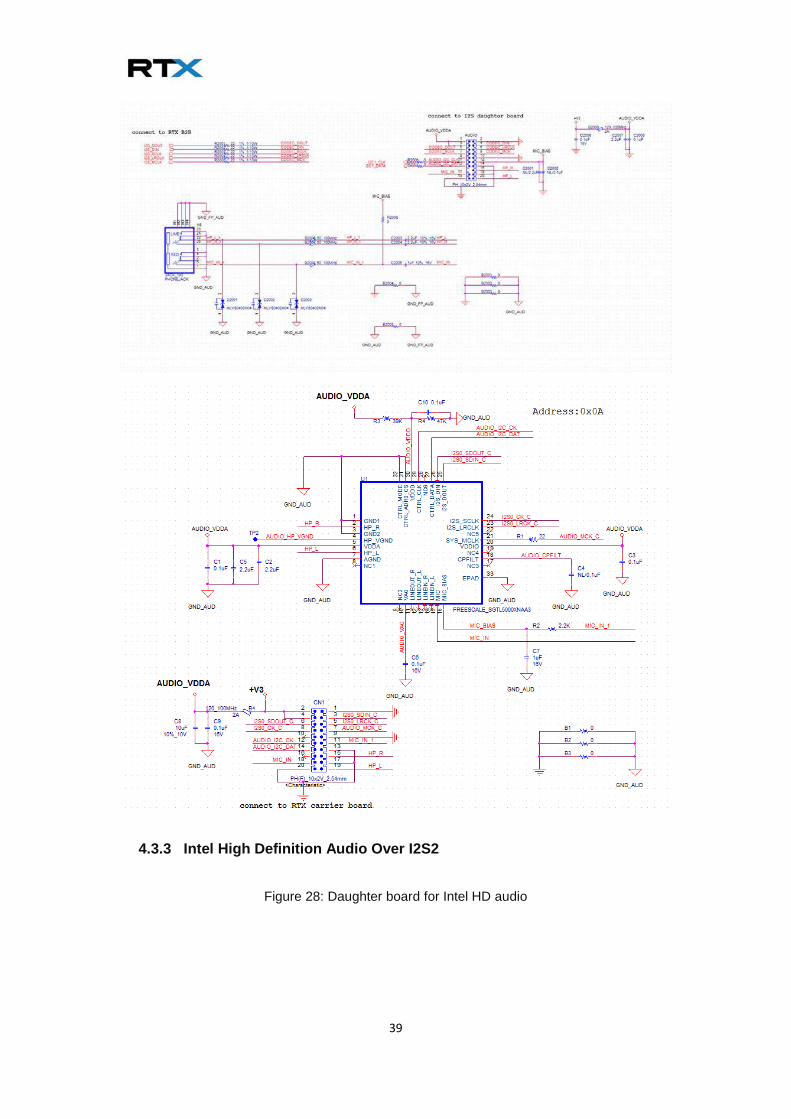
4.3.3 Intel High Definition Audio Over I2S2
Figure 28: Daughter board for Intel HD audio

40
4.4 4.4 SPI Interface 4.4.1 General
The Serial Peripheral Interface (SPI) bus is a full duplex synchronous serial communication
interface specification used for short distance communication. The interface was developed by
Motorola and has become a de facto standard. SPI devices communicate in full duplex mode
using a Master-Slave architecture with a single master. The master device originates the
frame for reading and writing. Multiple slave devices are supported through selection with
individual slave select by CS lines.
4.4.2 RTX Implementation
The RTX Module will be always the SPI master. And there are two SPI interfaces on RTX
Modules.
Figure 29: SPI ROM
4.5 CAN Bus 4.5.1 General
The Controller Area Network (CAN) is a serial communications protocol which efficiently
supports distributed real-time control with a very high level of security. Its domain of application
ranges from high speed networks to low cost multiple wiring. A maximum signaling rate is 1
Mbps.

41
4.5.2 RTX Implementation
The RTX spec support 2 logic level CAN ports. Carrier board is required to implement CAN
PHY as below. The connector is small form factor for demo board. This demo circuit shows
120 ohms terminations across the CAN pair.
Figure 30: CAN Bus transceiver
4.5.3 Isolation
The ISO 1050 is a galvanically isolated CAN transceiver that meets the specification
ISO11898-2 standard. The device has logic input and output buffers separated by a silicon
oxide (SiO2) insulation barrier that provides galvanic isolation of up 5000 Vrms for 1050DW
and 2500 Vrms 1050DUP.
5. High Speed Serial I/O Interfaces 5.1 USB Bus
5.1.1 General
The USB (Universal Serial Bus) is a hot-pluggable general purpose high speed I/O standard
for computer peripherals. The standard defines connector types (Type A, Type B, Mini-A,
Mini-B, Micro-A and Micro-B), cabling, and communication protocols for interconnecting a wide
variety of electronic devices.
The USB 2.0 Specification defines data transfer rates 480 Mbps (High Speed USB). A USB
host bus connector uses 4 pins: a power supply pin (5V) with 500mA, a differential pair (D+
and D- pins) and a ground pin. Additionally a fifth pin, USB ID for USB-OTG that may be used
which indicates whether the device operates in Host mode or a Client/Device mode.
The USB 3.0 Specification defines data rates 5 Gbps (Super Speed USB) that a USB host bus
connector uses 9 pins: a power supply pin (5V) with 900mA, 3 differential pairs (D+ and D-
pins for USB 2.0, SSRX+, SSRX-, SSTX+ and SSTX- for USB 3.0) and 2 ground pins.
RTX Modules support one USB 2.0 and one USB 3.0. USB 2.0 supports USB OTG feature.

42
USB 2.0 port can be configured as a host, client or OTG port. OTG operation is optional.
5.1.2 USB OTG
The figure 31 shows a USB-OTG implementation on the USB 2.0 port on a Mini USB Type B
connector. The ESD diodes should be placed close to the connector, and the USB differential
traces routed as differential pairs in “no stub” topology. The Common choke on differential pair
can reduce common mode emission for EMC radiation.
The Module USB_OTG_PWR_EN# signal controls the power switch with short circuit
protection, the Texas Instruments TPS2065 that current limit is between 1A and 1.9A. 70m
ohms Rds on resistance can help voltage drop.
Figure 31: USB 2.0 OTG
43
5.1.3 USB 2.0/USB 3.0 Host Ports
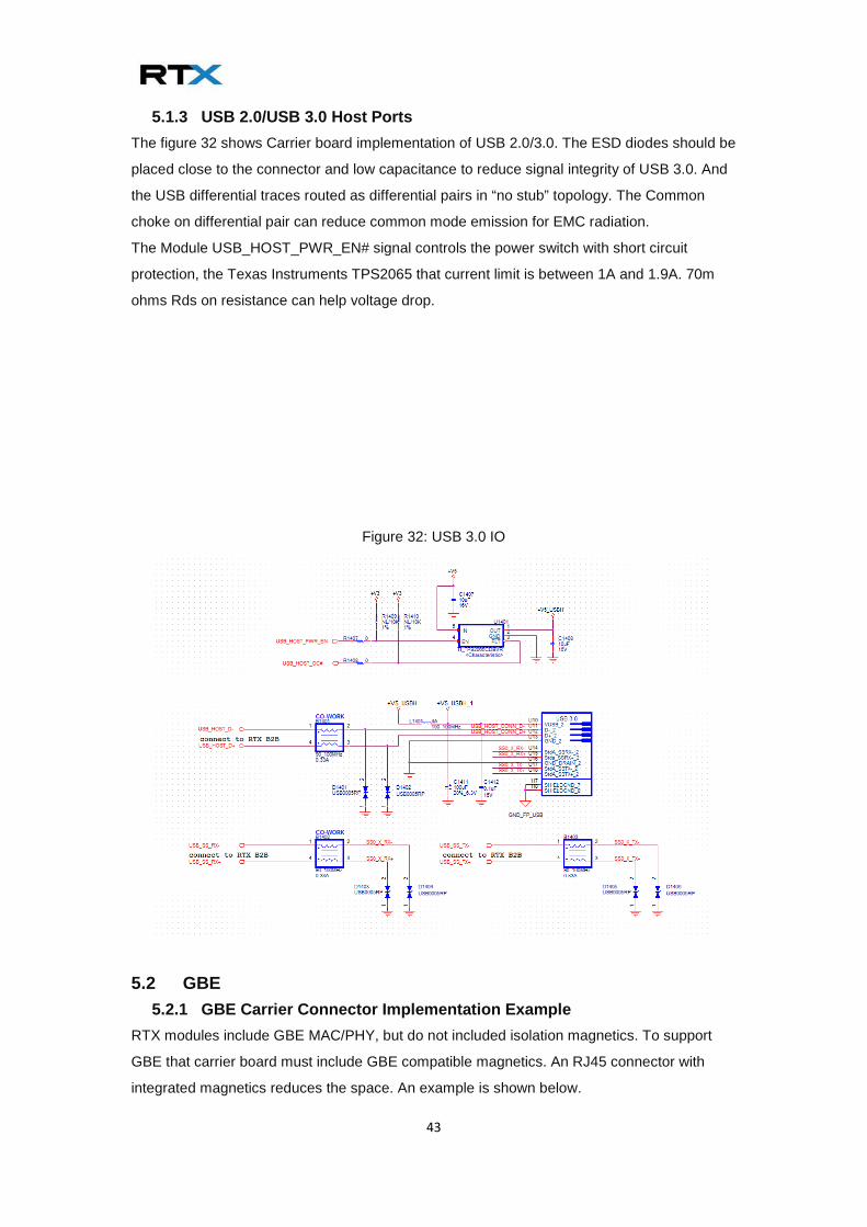
The figure 32 shows Carrier board implementation of USB 2.0/3.0. The ESD diodes should be
placed close to the connector and low capacitance to reduce signal integrity of USB 3.0. And
the USB differential traces routed as differential pairs in “no stub” topology. The Common
choke on differential pair can reduce common mode emission for EMC radiation.
The Module USB_HOST_PWR_EN# signal controls the power switch with short circuit
protection, the Texas Instruments TPS2065 that current limit is between 1A and 1.9A. 70m
ohms Rds on resistance can help voltage drop.
Figure 32: USB 3.0 IO
5.2 GBE 5.2.1 GBE Carrier Connector Implementation Example
RTX modules include GBE MAC/PHY, but do not included isolation magnetics. To support
GBE that carrier board must include GBE compatible magnetics. An RJ45 connector with
integrated magnetics reduces the space. An example is shown below.

44
Figure 33: GBE Application
5.2.2 GBE Mag-Jack Connector Recommendation
RTX GBE MAG-Jack (magnetics integrated into an RJ45 jack housing) should meet the
following general characteristics:

45
Turn ratios should be 1:1 +-2%. An integrated common mode choke should be
included.
Termination resistors and capacitors on the primary side (i.e. the Ethernet cable
side) should be included 75 ohms and 2KV Hi-voltage capacitors.
The secondary side transformer center-taps may be tied together or may be
brought out separately. If they are brought out separately, they are tied together on
the Carrier PCB.
The secondary side center-taps need to be tied to GBE_CTREF voltage, with
bypass capacitors connected to GND. Recommend electrical magnetics characteristics.
Table 4: Magnetics characteristics
Properties Test Condition Value Unit Tolerance
Inductance 100khz/100mV @ 8mA DC bias OCL 350 uH min.
Turn Ratio 100kHz/100mV TR 1:1 Tx
2% 1:1 Tx
Insertion Loss
100 kHz through 999 KHz
1.0 MHz through 60 MHz
60.1 MHz through 80MHz
80.1 MHz through 100 MHz
100.1 MHz through 120 MHz
IL
-1
-0.6
-0.8
-1.0
-2.4
dB max.
Return Loss
1~30MHz @100 ohms
30~60Mhz @100 ohms
60~80MHz @100 ohms
80~100Mhz @100 ohms
RL
-18
-14
-12
-10
dB min.
Common Mode
Rejection 1~100 MHz CMR -30 dB min.
Crosstalk 1~100 MHz CT -30 dB min.
5.2.3 GBE LEDs
Mag-Jack LED may be variable. Follow vendors spec to select parts to meet your product.
100M/1000G Link LED and Active LED are active low. Review LED sinking current and

46
resistance to meet power dissipation.
5.3 PCIe 5.3.1 General
The RTX provides X1 independent PCI Express* links (Port 0-1), which can be used
independently. The PCI Express topology consists of a transmitter (Tx) on one device
connected by a differential trace pair to a receiver (Rx) on a second device. One of the devices
may be located on the carrier board or on an add-in card. For more information on PCI
Express, refer to the PCI Express Base Specification, Rev. 2.0 and PCI Express Card
Electromechanical Specification, Rev. 2.0.
5.3.2 PCIe X1 add-in Card on Carrier
Figure 34 is an example for add-in cards.
Figure 34: PCIe X1
5.3.3 PCIe M.2 (TBD)

47
5.4 SATA 5.4.1 General
SATA defines a high-speed serialized ATA data link interface. The serialized interface uses
the command set from the ATA8-ACS standard, augmented with Native Command Queuing
commands optimized for the serialized interface. The serialized ATA interface is defined in a
register-compatible manner with parallel ATA to enable backward compatibility with parallel
ATA drivers. The physical interface is defined to ease integration (low pin count, low voltages)
and enable scalable performance (with currently defined data rates of 1.5 Gbps, 3.0 Gbps and
6.0 Gbps).
5.4.2 SATA Form Factor
Table 5: SATA Form Factor
Form Factor Key feature
SATA DOM
The application of SATA-DOM is space limitation, small formal factor and
embedded systems etc. It takes advantage of multi-level cell (MLC)
technology. The standard 7-pin SATA connection ensures speed
performance the built in error correcting code (ECC) and error detection
and correction (EDC) protect the data’s integrity.
SATA M.2 card
M.2 (formerly known as NGFF) is a small form factor card and connector
that supports applications such as Wi-Fi, WWAN, USB, PCIe & SATA, as
defined in the PCI-SIG M.2 Specification (see www.pcisig.com).
SATA SSD A SSD comes in traditional HDD form factors such as 3.5-inch, 2.5-inch
or 1.8-inch.

48
5.4.3 SATA-DOM
SATA-DOM is ideal for space limitation, small formal factor and embedded systems etc. It
takes advantage of multi-level cell (MLC) technology. The standard 7-pin SATA connection
ensures speedy performance and the built in error correcting code (ECC) and error detection
and correction (EDC) protects data integrity. In addition, it has no external cables, making it
more robust for various industrial and enterprise applications.
Figure 35: SATA-DOM
5.4.4 SATA Connector
Figure 36: SATA Connector

49
6. Memory Card Interfaces 6.1 SD Card The SD card is a memory card that is specifically designed to meet security, capacity,
performance, and environment requirements inherent in newly emerging audio and video
applications. The SD standard is maintained by the SD Card Association. In addition to the SD
Memory Card, there is the SD I/O (SDIO) Card. The SDIO Card specification is defined in a
separate specification named: "SDIO Card Specification" that can be obtained from the SD
Association. The SD Memory Card communication is based on an advanced 9-pin interface
(Clock, Command, 4xData and 3xPower lines) designed to operate at maximum operating
frequency of 50 MHz and low voltage ranges. RTX module supports SDIO as one of the BOOT
selections.
Figure 37: SD Card

50
6.2 eMMC The eMMC (embedded Multi-Media-Card) interface is used to connect non-volatile multimedia
memory devices to host processor. The eMMC standard is maintained by JEDEC, with the
latest revision being JESD84-B51: Embedded Multi-Media Card (eMMC), Electrical Standard
(Version 5.1).
An eMMC includes a raw MLC NAND flash memory and microcontroller. The eMMC
microcontroller performs several functions such as bad block management, wear leveling and
error correction code (ECC) internally which significantly reduces the software overhead.
RTX modules support 1 bit, 4 bit and 8 bit modes. The eMMC interface includes a clock line
(maximum clock frequency of 26 MHz or 52 MHz for devices supporting High Speed mode), a
command line and 8 data lines and an active low reset signal. RTX Modules support an eMMC
Boot option. The detail of eMMC specification revision should refer RTX module spec.
Figure 38 eMMC

51
7. Camera Interfaces 7.1 General The RTX specification allows for serial (MIPI CSI 2.0) and parallel cameras to be interfaced to
the RTX Module. The Module camera interface is at V_IO (typically 3.3v) or CSI voltage levels.
The same RTX pins are sharing for the serial and parallel interfaces, so some cautions are
necessary, as outlined in the RTX specification document and below Table 6. A given module

52
design will generally support either a serial or a parallel camera interface. In the long term, it is
expected that virtually all interfaces – including camera interfaces – will be serialized. MIPI
Alliance Standard for Camera Serial Interface CSI-2 in 2005 and CSI-3 in 2012. There are a
number of camera modules available that implement both serial and parallel interface formats
on the same device, set by a strap pin.
7.2 Camera Data Interface formats There are a wide variety of data formats that are used to convey camera data to a host system.
A complete description of these formats is much beyond the scope of this design guide. In
short, camera data formats may be divided into two groups: “raw” and “processed”. The raw
camera data formats need to be adjusted for camera and sensor specific characteristics.
Using the raw format requires an additional level of IPU (Image Processing Unit) and BT.656
or BT 1120 standard to process. Unless you have a specific need for a particular camera that
outputs “raw” sensor data, it is best to stick with cameras that include a processor on the
camera module that convert the camera sensor data to a standard format such as RGB or
YUV, JPEG or others. The “Bayer” format is one of the numerous raw formats that you may
wish to avoid. A variation on the above is that some cameras offer “raw” RGB, meaning that
the pixel data is sorted into RGB elements but sensor nonlinearities are not processed in the
camera IC.
7.3 Serial Camera Interface Example The figure below illustrates a CSI implementation on a RTX Carrier.
Figure 39: CSI module

53
7.4 Parallel Camera Interface Example
Figure 40: Parallel Camera Module

54
7.5 CSI/PCAM Pin Sharing
Table 6 CSI / PCAM Pin Assignment
Pin Location CSI PCAM
C29 CSI1_CK+ PCAM_D0
C27 CSI1_CK- PCAM_D1
C23 CSI1_D0+ PCAM_D2
C21 CSI1_D0- PCAM_D3
C17 CSI1_D1+ PCAM_D4
C15 CSI1_D1- PCAM_D5
C11 CSI1_D2+ PCAM_D6
C9 CSI1_D2- PCAM_D7
C5 CSI1_D3+ PCAM_D8
C3 CSI1_D3- PCAM_D9
C18 CSI0_CK+ PCAM_D10
C16 CSI0_CK- PCAM_D11
C12 CSI0_D0+ PCAM_D12
C10 CSI0_D0- PCAM_D13
C6 CSI0_D1+ PCAM_D14
C4 CSI0_D1- PCAM_D15

55
8. GPIO 8.1 RTX Module GPIO RTX Modules support eighteen general purpose IO pins: GPIO0 to GPIO17. Each of these can
be configured as an input or output pin. The RTX specification recommends the use of GPIO0
to GPIO5 as outputs and the use of GPIO6 to GPIO9 as inputs. The others 8 GPIOs (GPIO10
to GPIO17) are multiplexed pins supporting keypad. GPIO voltage level is 3.3V.
8.2 RTX GPIO multi-function Pin Sharing for Keypad
Table 7 GPIO multi-function Pin Assignment
Pin Location GPIO Signal Multi-Function with
B83 GPIO10 Keypad COL0
B85 GPIO11 Keypad COL1
B87 GPIO12 Keypad COL2
B89 GPIO13 Keypad COL3
B91 GPIO14 Keypad ROW0
B93 GPIO15 Keypad ROW1
B95 GPIO16 Keypad ROW2
B97 GPIO17 Keypad ROW3
Figure 41: Keypad
56
9. System Bus Interface 9.1 General System bus support PC104 connector with 31 bits of address and 16 bits of data.
9.2 Support
10. Thermal Design and Management
10.1 General RTX Modules generally have less power dissipations that are ranging from 2W to 6W for ARM
based designs. The Heat Spreader should cool down the RISC CPU to meet thermal
specifications and run in a room-temperature environment. In a production environment and
extreme environment, heat-sink and airflow is usually necessary to keep the Module RISC
CPU die temperatures within the recommended specification.
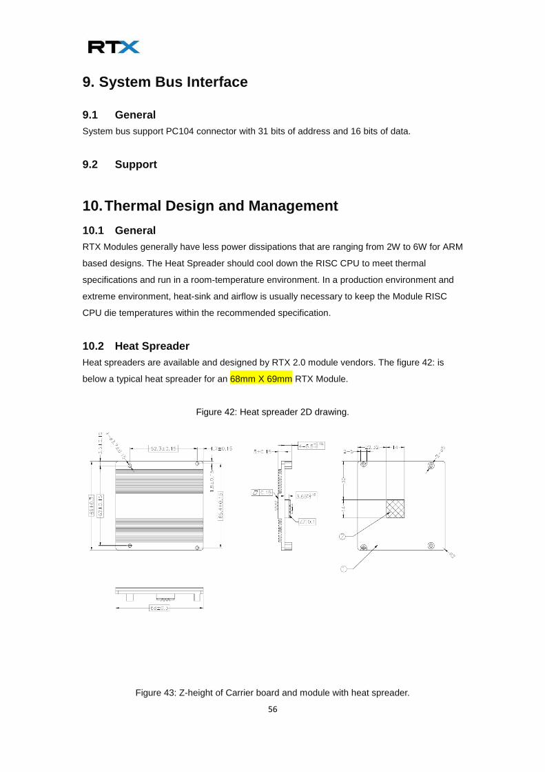
10.2 Heat Spreader Heat spreaders are available and designed by RTX 2.0 module vendors. The figure 42: is
below a typical heat spreader for an 68mm X 69mm RTX Module.
Figure 42: Heat spreader 2D drawing.
Figure 43: Z-height of Carrier board and module with heat spreader.

57
10.3 Thermal Resistance Calculations Thermal performance means collecting resistance data from vendors. The thermal resistance
vendors include silicon vendors, heat spreader, TIM (Thermal Interface Material), carrier board
vender and heat sink vendors.
According Ohm’s law and electrical resistance, thermal resistance is defined in degrees
Celsius per Watt (0 °C/W). For instance, Thermal resistance is 10 °C/W and the source device
dissipates 5W. The temperature rises 10 °C/W*5W=50 °C across that interface.
Table 8 Thermal Table
Parameter Symbol Value
Max SOC Junction Temperature (Tj) TJ-MAX 105 °C
Thermal Resistance, CPU Junction to
ambient θJA 15 °C/W
Thermal Resistance, CPU Junction to case θJC 0.4 °C/W
TIM interface (SOC to heat spreader) θTM 0.5 °C/W
Heat Spreader θHS 8 °C/W
SOC maximum Power dissipation Wsoc-Max 5W
Maximum Environment Temperature TOP-MAX To be calculated
No heat sink
TOP-MAX = TJ-MAX – θJA * WSOC-MAX = 105 – 15*5= 30 °C
With Heat Spreader
TOP-MAX = TJ-MAX – (θJC + θTM + θHS )*WSOC-MAX = 105 – (0.4+0.5+8)*5= 60.5 °C

58
11. Carrier Board PCB Design Overview
11.1 General PCB Stack-up and consideration This section presents an example stack-up for a carrier board based on the RTX 2.0 Module
form factor.
Note: The Document provides signal routing trace length on the board level only. The
maximum length listed in the routing guidelines for various interfaces does not account for
package trace length. Customers are requested to use Trace Length Calculator (TLC) for RTX
2.0 Module and Carrier board for maximum length calculations.
Note: If the guidelines are followed, measure critical signals to ensure proper signal integrity
and flight timing.
11.2 Six Layers PCB Stack-up A platform based on the RTX 2.0 Module requires a board stack-up yielding a target nominal
impedance for differential signals and single-ended signals. The platform should also target
the trace widths and spacing to meet the routing specification shown in Table 9. The stack-up
numbers may vary due to PCB material difference and type, thus it is important to work with
your PCB venders to fine tune with the specified impedance tolerances. Recommendations
are based on the 6-layer board stack-up in Figure 44 and Table 9
.
Figure 44: Six Layer PCB Stack-Up Example of 1.6mm (62 mils) Thick PCB

59
11.3 Trace Parameters for High Speed Differential Interface Table 9: Impedance Table and Trace Width/Spacing of 1.6 mm (62 mil) thick PCB
11.4 Trace Parameters for High Single Ended Interface (TBD)