rtl8204 realtek 3.3v single chip quad 10/100 …realtek.info/pdf/rtl8204.pdf · rtl8204 2001/12/06...
TRANSCRIPT

RTL8204
2001/12/06 1 Rev.1.1
REALTEK 3.3V SINGLE CHIP QUAD 10/100 MBPS
FAST ETHERNET TRANSCEIVER RTL8204
1. Features.....................................................................2 2. General Description .................................................2 3. Block Diagram..........................................................3 4. Pin Assignments .......................................................4 5. Pin Description .........................................................6
5.1 Media Connection pins........................................6 5.2 Power and Ground Pins.......................................6 5.3 Miscellaneous Pins..............................................7 5.4 RMII pins ............................................................7 5.5 SMI (Serial Management Interface) Pins ............7 5.6 LED Pins .............................................................8 5.7 Mode Pins ...........................................................8 5.8 Reserved Pins ......................................................8
6. Register Descriptions ...............................................9 6.1 Register0: Control ...............................................9 6.2 Register1: Status................................................10 6.3 Register2: PHY Identifier 1...............................10 6.4 Register3: PHY Identifier 2...............................11 6.5 Register4: Auto-Negotiation Advertisement..................11 6.6 Register5: Auto-Negotiation Link Partner Ability...............12
7. Functional Description ..........................................13 7.1 Initialization and Setup......................................13
7.1.1 Reset ..........................................................13 7.1.2 Setup and configuration.............................13
7.2 10Base-T ...........................................................13 7.2.1 Transmit Function......................................13 7.2.2 Receive Function .......................................13 7.2.3 Link Monitor..............................................14 7.2.4 Jabber.........................................................14
7.2.5 Loopback................................................... 14 7.3 100Base-TX...................................................... 14
7.3.1 Transmit Function ..................................... 14 7.3.2 Receive Function....................................... 15
7.4 100Base-FX...................................................... 15 7.4.1 Transmit function ...................................... 15 7.4.2 Receive function ....................................... 15 7.4.3 Far-End-Fault-Indication (FEFI)............... 15
7.5 RMII ................................................................. 16 7.6 SMI................................................................... 16 7.7 Power Saving and Power Down mode.............. 17
7.7.1 Power Saving mode................................... 17 7.7.2 Power Down mode.................................... 17 7.7.3 Additional Power Reduction ..................... 17
7.8 LED configuration............................................ 17 8. Application information........................................ 18
8.1 10Base-T/100Base-TX ..................................... 18 8.2 10Base-T/100Base-TX (Power Reduction) ...... 18 8.3 100Base-FX...................................................... 19
9. Electrical Characteristics...................................... 20 9.1 Absolute Maximum Ratings: ............................ 20 9.2 Operating Range:.............................................. 20 9.3 DC Characteristics ............................................ 20 9.4 AC Characteristics ............................................ 21 9.5 Digital Timing Characteristics.......................... 22 9.6 Thermal Data .................................................... 22
10. 100 Pin PQFP dimensions................................... 23 11. Document Revision Information ........................ 24

RTL8204
2001/12/06 2 Rev.1.1
1. Features Supports 4-port integrated physical layer and
transceiver for 10Base-T and 100Base-TX.
One port supports 100Base-FX.
Fully compliant with IEEE 802.3/802.3u.
Supports RMII (Reduced MII ) interface.
Low power consumption of 3.3V operating voltage.
Supports three Power reduction methods:
Power saving mode (cable detection).
Power down mode.
Selectable additional power reduction by 1.25:1
transformer on transmit side.
On-chip filtering eliminates the need for external
filters.
IEEE 802.3u compliant auto-negotiation for full
10/100 Mbps control.
Hardware controlled 10/100, Full/Half duplex, Flow
control advertisement ability.
Reversible PHY address.
Power-on auto reset function eliminates the need for
any external reset circuits.
Flashing LEDs for power-on diagnostics.
100-pin PQFP.
0.35 um, 3.3V CMOS technology.
2. General Description
The RTL8204 is a highly integrated 3.3V low power, 4 port, 10Base-T/100Base-TX/FX, Ethernet transceiver implemented in
0.35um CMOS technology. Flexible hardware settings are provided to configure the various operating modes of the RTL8204.
The RTL8204 consists of 4 separate and independent channels. Each channel consists of 4B5B encoder/decoder, Manchester
encoder/decoder, scrambler/descrambler, transmit output driver, output wave shaping, filters, digital adaptive equalizer, PLL
circuit and DC restoration circuit for clock/data recovery, and RMII interface to MAC controller. Moreover, the RTL8204
features very low power consumption, as low as 1.6 W (max.). Further power reduction can be accomplished via a 1.25:1
transformer on the transmit side, reducing power consumption to 1.28 W (max.).
For ease of system design, only one external clock source is needed when operating with the Realtek 8-port switch controller,
RTL8308, to produce a high performance switch system. Additionally, optimized pin outs are taken such that direct routing
can be implemented, which simplifies the layout work and reduces EMI noise issues. Finally, an on-chip filtering and wave
shaping circuit eliminates the need for many external components.

RTL8204
2001/12/06 3 Rev.1.1
3. Block Diagram
ADAPTIVE EQUALIZER
CLOCK RECOVERY
SERIAL-TO-PARALLEL
DESCRAMBLER
MII-TO-RMII CONVERSION
4B/5BDECODE
RMII-TO-MII CONVERSION
4B/5B ENCODER
SCAMBLER
PARALLEL-TO-SERIAL
MLT3ENCODER
10/100TX
DRIVER
BYP-DESCR
RXSTATE
MACHINE
RXD[3:0]
CRS
RXDV
RXD[1:0]
CRSDV
TXSTATE
MACHINE
COLTXCLKTXENTXER
RXCLK
TXD[3:0]
BYP-SCR
100BASE-TX TRANSMITTER
100BASE-TX RECEIVER
TXEN
TXD[1:0]
FXRP/NSDP/N
(PORT[D]ONLY)
RXIP/N
TXOP/N

RTL8204
2001/12/06 4 Rev.1.1
4. Pin Assignments
1 RXIN[A]
8 AVDD
80 DVDD 79 RXD[0][A] 78 RXD[1][A]
77 DVDD 76 TXE[B] 75 TXD[0][B]
74 TXD[1][B] 73 DGND
72 DGND 71 CRSDV[B]
69 RXD[0][B] 68 RXD[1][B]
67 DVDD 66 REFCLK
RTL8204
2 RXIP[A] 3 AGND
4 AGND5 TXOP[A]6 TXON[A]
7 AVDD
9 TXON[B] 10 TXOP[B]
11 AGND 12 AGND
13 RXIP[B] 14 RXIN[B] 15 AVDD
30 RXIN[D] 29 RXIP[D]
28 AGND 27 AGND
26 TXOP[D] 25 TXON[D] 24 AVDD
23 AVDD 22 TXON[C] 21 TXOP[C] 20 AGND 19 AGND 18 RXIP[C] 17 RXIN[C] 16 AVDD
31 AVDD 32 SDP[D]/TST[0] 33 SDN[D]/TST[1] 34 FXRP[D]/TST[2]
35 FXRN[D]/TST[3] 36 FXTP[D]
37 FXTN[D] 38 DPX[D] 39 ACT[D]/ANEG
40 SPD[D]/TEST# 41 DPX[C]/DPLX 42 ACT[C]/PAUSE 43 SPD[C]/FORCE100
44 DVDD 45 RXD[1][D] 46 RXD[0][D]
47 RXER[D]/PHYAD_RV# 48 CRSDV[D]
49 DGND 50 TXD[1][D]
51 TXD[0][D] 52 DGND
53 TXE[D] 54 DVDD 55 RXD[1][C]
56 RXD[0][C] 57 RXER[C]
58 CRSDV[C] 59 DGND
60 TXD[1][C] 61 TXD[0][C]
62 DVDD 63 TXE[C] 64 MDIO
65 MDC
70 RXER[B]
89 ACT[B]/PHYAD[3]
97 IBREF
100 AVDD
84 TXD[1][A]
90 SPD[B]/PHYAD[2]
95 RESET#
85 TXD[0][A] 86 TXE[A]
99 AVDD
81 RXER[A] 82 CRSDV[A] 83 DGND
87 DGND
94 RESERVED
91 DPX[A]/FX_DIS 92 ACT[A] 93 SPD[A]
96 AGND
98 AVDD
88 DPX[B]/PHYAD[4]

RTL8204
2001/12/06 5 Rev.1.1
'I' stands for input; 'O' stands for output; 'A' stands for analog; ‘D’ stands for digital PIN NAME PIN# TYPE PIN NAME PIN# TYPE RXIN[A], RXIP[A], AGND, AGND, TXOP[A], TXON[A], AVDD, AVDD, TXON[B], TXOP[B], AGND, AGND, RXIP[B], RXIN[B], AVDD, AVDD, RXIN[C]. RXIP[C], AGND, AGND, TXOP[C], TXON[C], AVDD, AVDD, TXON[D], TXOP[D], AGND, AGND, RXIP[D], RXIN[D], AVDD, SDP[D], SDN[D], FXRP[D], FXRN[D], FXTP[D], FXTN[D], DPX[D], ACT[D]/ANEG, SPD[D]/TEST#, DPX[C]/DPLX, ACT[C]/PAUSE, SPD[C]/FORCE100, DVDD, RXD[1][D], RXD[0][D], RXER[D]/PHYAD_RV# CRSDV[D], DGND, TXD[1][D],
1, 2, 3, 4, 5, 6, 7, 8, 9, 10, 11, 12, 13, 14, 15, 16, 17, 18, 19, 20, 21, 22, 23, 24, 25, 26, 27, 28, 29, 30, 31, 32, 33, 34, 35, 36, 37, 38, 39, 40, 41, 42, 43, 44, 45, 46, 47, 48, 49, 50,
AI AI
AGND AGND
AO AO
AVDD AVDD
AO AO
AGND AGND
AI AI
AVDD AVDD
AI AI
AGND AGND
AO AO
AVDD AVDD
AO AO
AGND AGND
AI AI
AVDD AI/O AI/O AI/O AI/O AO AO I/O I/O I/O I/O I/O I/O
DVDD O O
I/O O
DGND I
TXD[0][D], DGND, TXE[D], DVDD, RXD[1][C], RXD[0][C], RXER[C], CRSDV[C], DGND, TXD[1][C], TXD[0][C], DVDD, TXE[C], MDIO, MDC, REFCLK, DVDD, RXD[1][B], RXD[0][B], RXER[B], CRSDV[B], DGND, DGND, TXD[1][B], TXD[0][B], TXE[B], DVDD, RXD[1][A], RXD[0][A], DVDD, RXER[A], CRSDV[A], DGND, TXD[1][A], TXD[0][A], TXE[A], DGND, DPX[B]/PHYAD[4], ACT[B]/PHYAD[3], SPD[B]/PHYAD[2], DPX[A]/FX_DIS, ACT[A], SPD[A], RESERVED, RESET#, AGND, IBREF, AVDD, AVDD, AVDD
51 52, 53, 54, 55, 56, 57, 58, 59, 60, 61, 62, 63, 64, 65, 66, 67, 68, 69, 70, 71, 72, 73, 74, 75, 76, 77, 78, 79 80, 81, 82, 83, 84, 85, 86, 87, 88, 89, 90, 91, 92, 93, 94, 95, 96, 97, 98, 99, 100
I DGND
I DVDD
O O
I/O O
DGND I I
DVDD I
I/O I I
DVDD O O
I/O O
DGND DGND
I I I
DVDD O O
DVDD O O
DGND I I I
DGND I/O I/O I/O I/O I/O I/O I/O I
AGND AI/O
AVDD AVDD AVDD

RTL8204
2001/12/06 6 Rev.1.1
5. Pin Description Note that some pins are used for more than one function. Refer to the Pin Assignment diagram for a graphical representation.
'I' stands for input 'O' stands for output 'A' stands for analog signal 'D' stands for digital signal
5.1 Media Connection pins
PIN NAME Pin TYPE DESCRIPTION RXIP[A], RXIN[A] RXIP[B], RXIN[B] RXIP[C], RXIN[C] RXIP[D], RXIN[D]
2,1 13,14 18,17 29,30
AI Differential Receive Data Input
TXOP[A], TXON[A] TXOP[B], TXON[B] TXOP[C], TXON[C] TXOP[D], TXON[D]
5,6 10,9 21,22 26,25
AO Differential Transmit Data Output
FXRP[D],FXRN[D], FXTP[D],FXTN[D]
34,35 36,37
AI AO
Differential Receive Data Input for 100Base-FX. (port D) Differential Transmit Data Output for 100Base-FX. (port D)
SDP[D],SDN[D] 32,33 AI Signal Detect Input. (port D): When signal quality is good, SDP pin should be driven high relative to SDN pin.
5.2 Power and Ground Pins
PIN NAME Pin TYPE DESCRIPTION AVDD 7,8,15
16,23 24,31, 98,99, 100
P 3.3V power supply for Analog circuit
AGND 3,4,11, 12,19, 20,27, 28,96
G Ground for Analog circuit
DVDD 44,54, 62,67, 77,80
P Digital 3.3V power supply
DGND 49,52, 59,72, 73,83, 87
G Digital ground

RTL8204
2001/12/06 7 Rev.1.1
5.3 Miscellaneous Pins
PIN NAME Pin TYPE DESCRIPTION RESET# 95 I Reset is an active low input. To complete the reset function, this pin
must be asserted low for at least 10ms. The internal power-on auto reset circuit can reset the chip while the reset pin (pin95) is floating. To guarantee a successful auto-reset, the VCC rise from 0V to 2V should last at least 1ms.
REFCLK 66 I 50 MHz 100ppm Reference Clock Input IBREF 97 A Reference Bias Resistor: This pin must be tied to analog ground
through an external 1.96KΩ resistor when using a 1:1 transformer on Tx/Rx. For additional power reduction, use a 2.45 KΩ resistor with a 1.25:1 transformer. Refer to Additional Power Reduction section for more details.
5.4 RMII pins
PIN NAME Pin TYPE DESCRIPTION TXD[1:0][A] TXD[1:0][B] TXD[1:0][C] TXD[1:0][D]
84,85 74,75 60,61 50,51
I Transmit Data Input. The MAC will source TXD[1:0][n] synchronous to REFCLK when the corresponding TXE[n] is asserted.
TXE[A:D] 86, 76, 63, 53
I Transmit Enable. TXE[n] is asserted high by MAC to indicate valid data on TXD[1:0][n]
RXD[1:0][A] RXD[1:0][B] RXD[1:0][C] RXD[1:0][D]
78,79 68,69 55,56 45,46
O Receive Data Output. RTL8204 will source RXD[1:0][n] synchronous to REFCLK when the corresponding CRSDV[n] is asserted.
CRSDV[A:D] 82,71, 58,48
O Carrier Sense and Receive Data Valid
RXER[A:D] 81,70, 57,47
O Receive Error [A:D] Will assert high when receive symbol error occurs. The corresponding port RXD[1:0][n] will be 2’b2, while RXER[n] is set.
5.5 SMI (Serial Management Interface) Pins
PIN NAME Pin TYPE DESCRIPTION MDIO 64 I/O Management Data I/O: Bi-directional data interface. A 1.5KΩ
pull-up resistor is required (as specified in IEEE802.3u). The MAC controller access of the MII registers should be delayed at least 700us after completion of the reset because of the internal reset operation of RTL8204.
MDC 65 I Management Data Clock: 0 to 25MHz clock sourced by MAC to sample MDIO. The MAC controller access of the MII registers should be delayed at least 700us after completion of the reset because of the internal reset operation of RTL8204.

RTL8204
2001/12/06 8 Rev.1.1
5.6 LED Pins (LEDs activate as active high or low depending on mode pins. Refer to the LED configuration section) PIN NAME Pin TYPE DESCRIPTION DPX[A] DPX[B] DPX[C] DPX[D]
91 88 41 38
I/O Port [n] Duplex/Collision LED: Active state indicates Full Duplex mode or Collision when in Half Duplex mode. In 10Base-T, Collision LED blinks while Jabber happens.
ACT[A] ACT[B] ACT[C] ACT[D]
92 89 42 39
I/O Port [n] Activity/Link LED: Active state indicates a valid link. When there is receive or transmit activity, the LED will toggle between high and low.
SPD[A] SPD[B] SPD[C] SPD[D]
93 90 43 40
I/O Port [n] Speed LED: Active state indicates 100Base-TX mode.
5.7 Mode Pins PIN NAME Pin TYPE DESCRIPTION FX_DIS 91 I/O FX_DIS (FX Mode): Pulled low upon reset will put Port[D] in
100Base-FX mode. PHYAD[4] PHYAD[3] PHYAD[2]
88 89 90
I/O PHY Address. These 3 bits determine the highest 3 bits of 5-bit PHY address upon reset. Refer to Pin 47 PHYAD_RV# setting.
PHYAD_RV# 47 I/O PHY Address Reverse Mode: This pin is used to set the sequence of the PHY addresses upon reset. When low, the PHY addresses are assigned internally to port [A:D] as:
(XXX)11, (XXX)10, (XXX)01, (XXX)00. When high, the PHY addresses are assigned as:
(XXX)00, (XXX)01, (XXX)10, (XXX)11. Where (XXX) is PHYAD [4:2]
FORCE100 43 I/O FORCE100: Force 100Base-TX Operation. This pin works in conjunction with ANEG. When ANEG is low, this pin sets Reg.0.13. When ANEG is high, FORCE100 has no operational function. ANEG FORCE100 Resultant operation Low High All ports are forced to 100Base-TX Low Low All ports are forced to 10Base-T High Any FORCE100 is ignored
PAUSE 42 I/O PAUSE: Upon reset, this pin sets Reg.4.10. It is used to advertise to an auto-negotiation link partner that the MAC sublayer has pause/flow control capability when set in full duplex mode.
DPLX 41 I/O DPLX: Force Full Duplex Mode Enable. Upon reset, this pin 1) sets the default values of Reg.0.8 if ANEG is low, and 2) sets Nway full-duplex ability on Reg.4.8 and Reg.4.6 if ANEG is high.
TEST# 40 I/O TEST#: When low, the RTL8204 is configured in test mode. When high, it is in normal mode. This pin is reserved for internal testing only.
ANEG 39 I/O ANEG: Auto-Negotiation Enable. Upon reset, this pin sets Reg.0.12. Asserted high means auto-negotiation is enabled while low means manual selection through DPLX and FORCE100 pins.
5.8 Reserved Pins PIN NAME Pin TYPE DESCRIPTION Reserved 94 Reserved for internal use. Must be floating.

RTL8204
2001/12/06 9 Rev.1.1
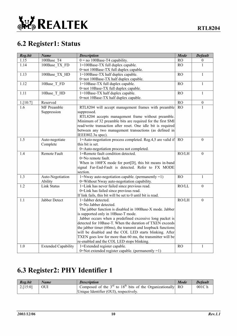
6. Register Descriptions The first six registers of the MII registers are defined by the MII specification. Other registers are defined by Realtek Semiconductor Corp. for internal use and are reserved for specific use.
Register Description Default 0 Control Register 1 Status Register 2 PHY Identifier 1 Register 3 PHY Identifier 2 Register 4 Auto-Negotiation Advertisement Register 5 Auto-Negotiation Link Partner Ability Register
RO: Read Only RW: Read/Write LL: Latch Low until cleared LH: Latch High until cleared SC: Self Clearing
6.1 Register0: Control Reg.bit Name Description Mode Default 0.15 Reset 1=PHY reset. This bit is self-clearing. RW/SC 0 0.14 Loopback 1=Enable loopback. This will loopback TXD to RXD and
ignore all the activities on the cable media. Loopback mode is only valid for 10Base-T. 0=Normal operation.
RW 0
0.13 Spd_Sel Speed select: 1=100Mbps 0=10Mbps When Nway is enabled, this bit reflects the result of auto-negotiation. (Read only) When Nway is disabled, this bit can be set by FORCE100 (pin43) or SMI*. (Read/Write) For port[D], when 100FX mode is enabled by pulling FX_DIS (pin91) low, this bit =1 regardless if Nway is enabled or not. (Read only)
RW Set by FORCE100
(pin 43) or
1 for 100FX
0.12 Auto Negotiation Enable
1 = Enable auto-negotiation process. 0 = disable auto-negotiation process. This bit can be set by ANEG (pin39) or SMI.(Read/Write) For port[D], when 100FX mode is enabled by pulling FX_DIS (pin91) low, this bit =0 regardless if ANEG (pin39) is pulled high or low. (Read only)
RW Set by ANEG
(pin 39) or
0 for 100FX
0.11 Power Down 1=Power down. All functions will be disabled except SMI. 0=Normal operation.
RW 0
0.10 Isolate 1 = Electrically isolate the PHY from RMII. PHY is still able to respond to MDC/MDIO. 0 = Normal operation
RW 0
0.9 Restart Auto Negotiation
1=Restart Auto-Negotiation process. 0=Normal operation.
RW/SC 0
0.8 Duplex Mode 1=Full duplex operation. 0=Half duplex operation. When Nway is enabled, this bit reflects the result of auto-negotiation. (Read only) When Nway is disabled or 100FX enabled (port[D] only), this bit can be set by DPLX (pin41) or SMI. (Read/Write).
RW Set by DPLX
(pin 41)
0.[7:0] Reserved 0 *SMI: Serial Management Interface, which is composed of MDC,MDIO, allows MAC to manage PHY.
RTL8204
2001/12/06 10 Rev.1.1
6.2 Register1: Status Reg.bit Name Description Mode Default 1.15 100Base_T4 0 = no 100Base-T4 capability. RO 0 1.14 100Base_TX_FD 1=100Base-TX full duplex capable.
0=not 100Base-TX full duplex capable. RO 1
1.13 100Base_TX_HD 1=100Base-TX half duplex capable. 0=not 100Base-TX half duplex capable.
RO 1
1.12 10Base_T_FD 1=10Base-TX full duplex capable. 0=not 10Base-TX full duplex capable.
RO 1
1.11 10Base_T_HD 1=10Base-TX half duplex capable. 0=not 10Base-TX half duplex capable.
RO 1
1.[10:7] Reserved RO 0 1.6 MF Preamble
Suppression RTL8204 will accept management frames with preamble suppressed. RTL8204 accepts management frame without preamble. Minimum of 32 preamble bits are required for the first SMI read/write transaction after reset. One idle bit is required between any two management transactions (as defined in IEEE802.3u spec).
RO 1
1.5 Auto-negotiate Complete
1=Auto-negotiation process completed. Reg.4,5 are valid if this bit is set. 0=Auto-negotiation process not completed.
RO 0
1.4 Remote Fault 1=Remote fault condition detected. 0=No remote fault. When in 100FX mode for port[D], this bit means in-band signal Far-End-Fault is detected. Refer to FX MODE section.
RO/LH 0
1.3 Auto-Negotiation Ability
1=Nway auto-negotiation capable. (permanently =1) 0=Without Nway auto-negotiation capability.
RO 1
1.2 Link Status 1=Link has never failed since previous read. 0=Link has failed since previous read. If link fails, this bit will be set to 0 until bit is read.
RO/LL 0
1.1 Jabber Detect 1=Jabber detected. 0=No Jabber detected. The jabber function is disabled in 100Base-X mode. Jabber is supported only in 10Base-T mode. Jabber occurs when a predefined excessive long packet is detected for 10Base-T. When the duration of TXEN exceeds the jabber timer (60ms), the transmit and loopback functions will be disabled and the COL LED starts blinking. After TXEN goes low for more than 60 ms, the transmitter will be re-enabled and the COL LED stops blinking.
RO/LH 0
1.0 Extended Capability 1=Extended register capable. 0=Not extended register capable. (permanently =1)
RO 1
6.3 Register2: PHY Identifier 1 Reg.bit Name Description Mode Default 2.[15:0] OUI Composed of the 3rd to 18th bits of the Organizationally
Unique Identifier (OUI), respectively. RO 001C h

RTL8204
2001/12/06 11 Rev.1.1
6.4 Register3: PHY Identifier 2 Reg.bit Name Description Mode Default 3.[15:10] OUI Assigned to the 19th through 24th bits of the OUI. RO 110010 b 3.[9:4] Model Number Manufacturer's model number 04. RO 000100 b 3.[3:0] Revision Number Manufacturer's revision number 01. RO 0001 b
6.5 Register4: Auto-Negotiation Advertisement This register contains the advertisement abilities of this device as they will be transmitted to its link partner during Auto-negotiation. Reg.bit Name Description Mode Default 4.15 Next Page 1=Next Page enabled.
0=Next Page disabled. (Permanently =0) RO 0
4.14 Acknowledge Permanently =0. RO 0 4.13 Remote Fault 1=Advertises that RTL8204 has detected a remote fault.
0=No remote fault detected. RW 0
4.[12:11] Reserved RO 0 4.10 Pause 1=Advertises that RTL8204 has flow control capability.
0=Without flow control capability. RW Set by
PAUSE (pin 42)
4.9 100Base-T4 Technology not supported. (Permanently =0) RO 0 4.8 100Base-TX-FD 1=100Base-TX full duplex capable.
0=Not 100Base-TX full duplex capable. RW Set by
DPLX (pin 41)
4.7 100Base-TX 1=100Base-TX half duplex capable. 0=Not 100Base-TX half duplex capable.
RW 1
4.6 10Base-T-FD 1=10Base-TX full duplex capable. 0=Not 10Base-TX full duplex capable.
RW Set by DPLX
(pin 41) 4.5 10Base-T 1=10Base-TX half duplex capable.
0=Not 10Base-TX half duplex capable. RW 1
4.[4:0] Selector Field [00001]=IEEE802.3 RO 00001

RTL8204
2001/12/06 12 Rev.1.1
6.6 Register5: Auto-Negotiation Link Partner Ability This register contains the advertised abilities of the Link Partner as received during Auto-negotiation. The content changes after the successful Auto-negotiation if Next-pages are supported. Reg.bit Name Description Mode Default 5.15 Next Page 1=Link partner desires Next Page transfer.
0=Link partner does not desire Next Page transfer. RO 0
5.14 Acknowledge 1=Link Partner acknowledges reception of FLP words. 0=Not acknowledged by Link Partner.
RO 0
5.13 Remote Fault 1=Remote Fault indicated by Link Partner. 0=No remote fault indicated by Link Partner.
RO 0
5.12-11 Reserved RO 0 5.10 Pause 1=Flow control supported by Link Partner.
0=No flow control supported by Link Partner. RO 0
5.9 100Base-T4 1=100Base-T4 supported by Link Partner. 0=100Base-T4 not supported by Link Partner.
RO 0
5.8 100Base-TX-FD 1=100Base-TX full duplex supported by Link Partner. 0=100Base-TX full duplex not supported by Link Partner. For port[D] 100FX mode, this bit is set when Reg.0.8=1. When Nway is disabled, this bit is set when Reg.0.13=1 and Reg.0.8=1.
RO 0
5.7 100Base-TX 1=100Base-TX half duplex supported by Link Partner. 0=100Base-TX half duplex not supported by Link Partner. For port[D] 100FX mode, this bit is set when Reg.0.8=0. When Nway is disabled, this bit is set when Reg.0.13=1 and Reg.0.8=0.
RO 0
5.6 10Base-T-FD 1=10Base-TX full duplex supported by Link Partner. 0=10Base-TX full duplex not supported by Link Partner. When Nway is disabled, this bit is set when Reg.0.13=0 and Reg.0.8=1.
RO 0
5.5 10Base-T 1=10Base-TX half duplex supported by Link Partner. 0=10Base-TX half duplex not supported by Link Partner. When Nway disabled, this bit is set when Reg.0.13=0,and Reg.0.8=0.
RO 0
5.[4:0] Selector Field [00001]=IEEE802.3 RO 00001

RTL8204
2001/12/06 13 Rev.1.1
7. Functional Description The RTL8204 is a four-port Ethernet transceiver that supports 10Mbps and 100Mbps applications. Upon power-up, the
RTL8204 determines its operation mode for each port. If Nway is enabled, RTL8204 uses auto-negotiation/parallel detection
on each port to automatically determine line speed, duplex and flow control ability. Each port can work on 10Mbps or
100Mbps with full-duplex or half-duplex mode independently to others. Port[D] can also be configured for 100Base-FX.
7.1 Initialization and Setup
7.1.1 Reset
The RTL8204 is initialized while in reset state. There are 3 ways to get the RTL8204 into reset: power-on reset, hardware
reset signal (asserted for at least 10ms), and software reset by setting MII Reg.0.15 bit. The RTL8204 flashes all LEDs once
to indicate completion of initialization. All setting values for operation modes are latched from corresponding mode pins at
the end of the reset cycle. The internal power-on auto reset circuit can reset the chip while the reset pin (pin95) is floating. To
guarantee a successful auto-reset, the VCC rise from 0V to 2V should last at least 1ms.
7.1.2 Setup and configuration
The RTL8204 operation mode can be configured either 1) by hardware pulled high or low; or 2) by software programming
via access of MII registers through SMI. Refer to the pin description and register description sections.
LED applications needs to be consistent with the pulled up/down mode pins. Refer to the LED configuration section.
7.2 10Base-T
Through Hardware/software setting or Nway, the RTL8204 can run in 10Base-T mode with all features compatible with
industry standards. There are no 4B/5B coding/decoding or scrambler/descrambler functions in 10Base-T.
7.2.1 Transmit Function
When TXEN is active, 2-bit TXD from RMII is serialized, Manchester-encoded, and driven into network medium as a packet
stream. An on-chip filtering and wave shaping circuit eliminates the need for external filtering. The transmit function is
disabled when the link has failed or when auto-negotiation proceeds.
7.2.2 Receive Function
The Manchester decoder converts the incoming serial stream when the squelch circuit detects the signal level above squelch
level, and serial-to-parallel logic generates 2-bit (RMII) data from the serial stream. The preamble of the incoming stream is
stripped off and regenerated. SFD is generated into RMII RXD once the incoming SFD is detected and data bits entering the

RTL8204
2001/12/06 14 Rev.1.1
elastic buffer are over the threshold.
7.2.3 Link Monitor
The 10Base-T link pulse detection circuit always monitors the RXIP/RXIN pins for the presence of valid link pulses.
Auto-polarity is implemented for correcting the detected reverse polarity of RXIP/RXIN signal pairs.
7.2.4 Jabber
Jabber occurs when TXEN is asserted over 60ms. Both transmit and loopback functions are disabled once jabber happens.
The MII Reg.1.1 (Jabber detect) bit is set high until jabber disappears and the bit is read again. The Jabber function is
supported in 10-Base-T only, and is not implemented in 100Base-TX. The collision LED of the corresponding port will blink
while Jabber happens. Jabber is dismissed after TXEN remains low for at least 60ms.
7.2.5 Loopback
Setting the MII Reg.0.14 enables the loopback mode. In loopback mode, TXD is transferred directly to RXD with TXEN
changed to CRS_DV. Incoming data stream from network medium is blocked in this mode. The loopback function is not
implemented in 100Base-TX/FX.
7.3 100Base-TX
Through Hardware/software setting or Nway, the RTL8204 can run in 100Base-TX mode with all features compatible with
industry standards. An internal 125MHz clock is generated by an on-chip PLL circuit to synchronize the transmit data or
generate the clock signal for the incoming data stream.
7.3.1 Transmit Function
Upon detection of TXEN high, the RTL8204 converts 2 di-bits to 5bit code-group and substitutes /J/K code-groups for the
first 2 code-groups, which is called SSD (Start-of-Stream-Delimiter). 4B/5B coding continues for all the data as long as
TXEN is asserted high. At the end of TXEN, /T/R code-groups are appended to the last data field, which will be stripped off
at the remote receiving side. During the inter-packet gap, where TXEN deasserted, IDLE code-groups are transmitted for the
sake of clocking of the remote receiver. The 5-bit serial data stream after 4B/5B coding is then scrambled as defined by the
TP-PMD Stream Cipher function to flatten the power spectrum energy such that EMI effects can be significantly reduced.
The scrambled seed is unique for each port based on PHY addresses. The scrambled bit stream is driven into network
medium in the form of MLT-3 signaling. The multi-level signaling technology moves the power spectrum energy from high
frequency to low frequency, which also benefits EMI emission. Scrambling is not implemented in 100Base-FX.

RTL8204
2001/12/06 15 Rev.1.1
7.3.2 Receive Function
The receive path includes a receiver composed of adaptive equalizer and DC restoration circuits. These circuits compensate
for incoming distortion of the MLT-3 signal. A MLT-3 to NRZI, and NRZI to NRZ converter is used to convert analog
signals to digital bit-stream. A PLL circuit is also included to clock data bits exactly with minimum bit error rate.
De-scrambler, 5B/4B decoder and serial-to-parallel conversion circuits follow. CRS_DV is asserted no later than when SSD
(Start-of-Stream-Delimiter) is detected within a few bits time, (delay due to the elastic buffer as mentioned in the RMII
section) and ends toggling once the data in the elastic buffer has been dumped to RMII RXD.
7.4 100Base-FX
Port[D] can be configured as 100Base-FX either through hardware configuration or software configuration. For port[D], the
priority of setting 100FX is greater than Nway. Scrambler is not needed in 100Base-FX.
7.4.1 Transmit function
In 100Base-FX transmit, di-bits of TXD are processed as 100Base-TX, except without scrambler, before the NRZI stage.
Instead of converting to MLT-3 signals as in 100Base-TX, the serial data stream is driven out as NRZI PECL signals, which
enters the fiber transceiver in differential-pairs form. The fiber transceiver should be available working in a 3.3V
environment. Refer to the fiber application section.
PECL DC characteristics Parameter Symbol Min Max Unit PECL Input High Voltage Vih Vdd-1.16 Vdd-0.88 V PECL Input Low Voltage Vil Vdd-1.81 Vdd-1.47 V PECL Output High Voltage Voh Vdd-1.02 V PECL Output Low Voltage Vol Vdd-1.62 V
7.4.2 Receive function
Signals are received through PECL receiver inputs from the fiber transceiver, and directly passed to the clock recovery circuit
for data/clock recovery. Scrambler/de-scrambler is bypassed in 100Base-FX.
7.4.3 Far-End-Fault-Indication (FEFI)
The MII Reg.1.4 (Remote Fault) is a FEFI bit for port[D] when 100FX is enabled, which indicates FEFI has been detected.
FEFI is an alternative in-band signaling which is composed of 84 consecutive ‘1’ followed by one ‘0’. From the RTL8204’s
view, once this pattern is detected 3 times, Reg.1.4 is set, which means the transmit path (Remote side’s receive path) has
some problems. On the other hand, to send a FEFI stream pattern, one of two conditions need to be satisfied: Either 1) SD
(Signal Detection) fails; or 2) it detects false carrier on RxOP/RxON pair, which will force the RTL8204 to start sending this

RTL8204
2001/12/06 16 Rev.1.1
pattern, which in turn will cause the remote side to detect a Far-End-Fault. This means the RTL8204 sees problems on the
receive path. The FEFI mechanism is used only in 100Base-FX.
7.5 RMII
The RTL8204 meets all the RMII requirements outlined in the RMII Consortium specifications. The main advantage
introduced by RMII is pin count reduction; e.g., it operates with only one 50Mhz reference clock for both the TX and RX
sides without separate clocks needed for the Tx and Rx paths, as with the MII interface. However, some hardware
modification is needed for this change, the most important and outstanding of which is the presence of an elastic buffer for
absorption of the frequency difference between the 50Mhz reference clock and the clocking information of the incoming data
stream. The clock information on the incoming data stream is not necessary for the PHY implemented with the MII interface.
Another change implemented is that the MII RXDV and CRS pins are merged into one signal, CRS_DV, which is asserted
high while detecting incoming packet data. Because of the timing difference between the incoming data and the output data
(presented on RMII RXD and caused from the introduction of the elastic buffer), the internal CRS signal is may be deasserted
with CRS_DV asserting when the incoming data ends. For this condition, CRS_DV toggles at a 25MHz rate for 100Base-TX
or 2.5MHz for 10Base-T (low for the first di-bit of nibble, high for second, etc.) until the last piece of data in the elastic
buffer is output onto RMII RXD. RXD[1:0] is substituted by 2’b10 while RXER is asserted.
7.6 SMI
SMI (Serial Management Interface) is also known as MII Management Interface, which consists of two signals, MDIO and
MDC; allowing the MAC controller to control and monitor the state of PHY. MDC is a clock input for PHY to latch MDIO
on its rising edge. The clock can run from DC to 25MHz. MDIO is a bi-directional connection used to write data to, or read
data from PHY. The PHY address base is set by pins PHYAD[4:2] and four ports addresses of RTL8204 are internally
00,01,10.11 or 11,10,01,00 respectively depending on whether PHY_RV# equals to 1 or 0 upon reset. SMI Read/Write Cycles Preamble
(32 bits) Start (2 bits)
OP Code (2 bits)
PHYAD (5 bits)
REGAD (5 bits)
TrunAround (2 bits)
Data (16 bits)
Idle
Read 1……..1 01 10 AAAAA RRRRR Z0 D…….D Z* Write 1……..1 01 01 AAAAA RRRRR 10 D…….D Z* *Z: high-impedance. During idle time, MDIO state is determined by an external 1.5KΩ pull-up resistor.
The RTL8204 supports Preamble Suppression, which allows the MAC to issue Read/Write Cycles without preamble bits.
However, for the first MII management cycle after power-on reset, 32-bit preamble are needed.
To guarantee the first successful SMI transaction after power-on reset, the MAC should be delayed at least 700us to issue the
first SMI Read/Write Cycle relative to the rising edge of reset.

RTL8204
2001/12/06 17 Rev.1.1
7.7 Power Saving and Power Down mode
7.7.1 Power Saving mode
The RTL8204 implements a power saving mode on a per port base. One port automatically enters power saving mode 10
seconds after the cable is disconnected from it, regardless of whether the RTL8204’s operation mode is Nway or Force mode.
Once one port enters power saving mode, it transmits normal link pulses only on its TXOP/TXON pins and keeps monitoring
RXIP/RXIN to try to detect any incoming signals, which might be 100Base-TX MLT-3 idle pattern, 10Base-T link pulses or
Nway’s FLP (fast link pulses). After it detects any incoming signals, it wakes up from the power saving mode and operates in
the normal mode according to the result of the connection.
7.7.2 Power Down mode
Setting MII Reg.0.11 forces RTL8204’s corresponding port entering power down mode, which disables all transmit/receive
functions and RMII functions on that port, except SMI (MDC/MDIO management interface).
7.7.3 Additional Power Reduction
Additional power reduction can be obtained by using a 1.25:1 transformer on the TX side and using a 2.45KΩ resistor on the
IBREF pin. External pull-high resistors for TXOP/TXON should be changed from 50Ω to 78Ω. Refer to application section
for more details. Maximum power consumption is reduced by about 20%. Both 10Base-T and 100Base-TX work well on
RTL8204 for 78Ω termination resisters when using this alternative configuration.
7.8 LED configuration
All LEDs flash once for about 320ms after power-on reset. All LEDs pins are dual function pins, which can be configured as
either active high or low by pulling them low or high accordingly. If the pin is pulled high; the LED is active low after reset.
Likewise, if the pin is pulled low; the LED is active high. The typical values for pull-up/down resistors are between 1K to
10K Ω. The example below shows an example to select PHYAD[4:2]=3’b010 and the circuits for LEDs.
VCC
GND GND
300Ω300Ω 300Ω
10ΚΩ 10ΚΩ 10ΚΩ
pin89: ACT[B]/PHYAD[3]
pin90: SPD[B]/PHYAD[2]pin88: DPX[B]/PHYAD[4]

RTL8204
2001/12/06 18 Rev.1.1
8. Application information
8.1 10Base-T/100Base-TX
8.2 10Base-T/100Base-TX (Power Reduction)
RTL8204
2001/12/06 19 Rev.1.1
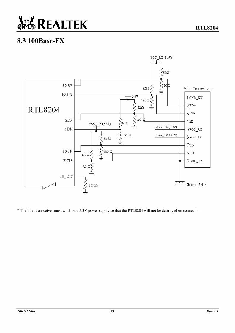
8.3 100Base-FX
* The fiber transceiver must work on a 3.3V power supply so that the RTL8204 will not be destroyed on connection.

RTL8204
2001/12/06 20 Rev.1.1
9. Electrical Characteristics
9.1 Absolute Maximum Ratings: WARNING: Absolute maximum ratings are limits beyond which may cause permanent damage to the device or affect device
reliability. All voltages are specified reference to GND unless otherwise specified. Parameter Min Max Units
Storage Temperature -55 +150 °C Vcc Supply Referenced to GND -0.5 +4.0 V Digital Input Voltage -0.5 Vcc V DC Output Voltage -0.5 Vcc V
9.2 Operating Range: Parameter Min Max Units
Ambient Operating Temperature(Ta) 0 +70 °C Vcc Supply Voltage Range(Vcc) 3.15 3.45 V
9.3 DC Characteristics (0°C<Ta<70°C, 3.15V<Vcc<3.45V)
Parameter SYM Conditions Min Typ Max Units Power Supply Current for
all 4 ports Icc 10 Base-T, idle
10 Base-T, Peak continuous 100% utilization 100 Base-TX, idle 100 Base-TX, Peak continuous 100% utilization 10/100 Base-TX, low power without cable Power down
208 461 342 357 66 46
mA
Power Consumption for all 4 ports
PS 10 Base-T, idle 10 Base-T, Peak continuous 100% utilization 100 Base-TX, idle 100 Base-TX, Peak continuous 100% utilization 10/100 Base-TX, low power without cable Power down
0.74 1.62 1.15 1.19 0.22 0.15
W
TTL Input High Voltage Vih 2.0 V TTL Input Low Voltage Vil 0.8 V
TTL Input Current Iin -50 50 uA TTL Input Capacitance Cin 5 pF
Output High Voltage Voh Vcc-0.4 V Output Low voltage Vol 0.4 V LED Output Current Ioh 10 mA LED Output Current Iol 12 mA
Parameter SYM Conditions Min Typ Max Units
Output Tristate Leakage Current
|IOZ| 10 uA
Transmitter, 100Base-TX (1:1 Transformer Ratio) TX+/- Output Current High IOH 40 mA TX+/- Output Current Low IOL 0 uA

RTL8204
2001/12/06 21 Rev.1.1
Transmitter, 10Base-T(1:1 Transformer Ratio)
TX+/- Output Current High IOH 100 mA TX+/- Output Current Low IOL 0 uA
Transmitter, 100Base-TX(1.25:1 Transformer Ratio) TX+/- Output Current High IOH 32 mA TX+/- Output Current Low IOL 0 uA
Transmitter, 10Base-T (1.25:1 Transformer Ratio) TX+/- Output Current High IOH 80 mA TX+/- Output Current Low IOL 0 uA
Receiver, 100Base-TX RX+/- Common-mode input
voltage 1.32 V
RX+/- Differential input resistance
20 kΩ
Receiver, 10BaseT Differential Input Resistance 20 kΩ
Input Squelch Threshold 340 mV
9.4 AC Characteristics (0°C<Ta<70°C, 3.15V<Vcc<3.45V)
Parameter SYM Conditions Min Typ Max Units Transmitter, 100Base-TX
Differential Output Voltage, peak-to-peak
VOD 50Ω from each output to Vcc, Best-fit over 14 bit times
1.9 2.03 2.1 V
Differential Output Voltage Symmetry
VOS 50Ω from each output to Vcc, |Vp+|/ |Vp-| 0.99 1 1.01 %
Differential Output Overshoot VOO
Percent of Vp+ or Vp- 3.43 5 %
Rise/Fall time tr,tf 10-90% of Vp+ or Vp- 3 3.8 5 ns Rise/Fall time imbalance |tr - tf| 200 500 ps
Duty Cycle Distortion Deviation from best-fit time-grid, 010101 … Sequence
±175 ±200 ps
Timing jitter Idle pattern 0.75 0.8 ns Transmitter, 10Base-T
Differential Output Voltage, peak-to-peak
VOD 50Ω from each output to Vcc, all pattern 4.5 5.06 5.5 V
TP_IDL Silence Duration Period of time from start of TP_IDL to link pulses or period of time between link pulses
13.6 15.6 16 ms
TD Short Circuit Fault Tolerance
Peak output current on TD short circuit for 10 seconds.
152 mA
TD Differential Output Impedance (return loss)
Return loss from 5MHz to 10MHz for reference resistance of 100 Ω.
26 40 dB
TD Common-Mode Output Voltage
Ecm Terminate each end with 50Ω resistive load. 45.6 50 mV
Transmitter Output Jitter 11.5 ns RD Differential Output Impedance (return loss)
Return loss from 5MHz to 10MHz for reference resistance of 100 Ω.
35 dB
Harmonic Content dB below fundamental, 20 cycles of all ones data
27 28 dB
Start-of-idle Pulse width TP_IDL width 280 330 ns

RTL8204
2001/12/06 22 Rev.1.1
9.5 Digital Timing Characteristics Parameter SYM Conditions Min Typ Max Units
100Base-TX Transmit System Timing Active TX_EN Sampled to
first bit of “J on MDI output
Bits
Inactive TX_EN Sampled to first bit of “T on MDI
output
Bits
TX Propagation Delay tTXpd From TXD[1:0] to TXOP/N Bits 100Base-TX Receive System Timing
First bit of “J on MDI input to CRS_DV assert
From RXIP/N to CRS_DV 6 8 Bits
First bit of “T on MDI input to CRS_DV de-assert
From RXIP/N to CRS_DV 16 18 Bits
RX Propagation Delay tRXpd From RXIP/N to RXD[1:0] 15 17 Bits 10Base-T Transmit System Timing
TX Propagation Delay tTXpd From TXD[1:0] to TXOP/N 5 6 Bits TXEN to MDI output From TXEN assert to TXOP/N 5 6 Bits
10Base-T Receive System Timing Carrier Sense Turn-on
delay tCSON Preamble on RXIP/N to CRS_DV asserted 12 Bits
Carrier Sense Turn-off Delay
tCSOFF TP_IDL to CRS_DV de-asserted 8 9 Bits
RX Propagation Delay tRXpd From RXIP/N to RXD[1:0] 9 12 Bits LED timing
LED On Time tLEDon While LED blinking 43 ms LED Off Time tLEDoff While LED blinking 43 ms
Jabber timing (10Base-T only) Jabber Active From TXEN=1 to Jabber asserted 60 70 80 ms
Jabber de-assert From TXEN=0 to Jabber de-asserted 60 86 ms RMII Timing
TXD, TXEN Setup time TXD [1:0], TXEN to REFCLK rising edge setup time
4 ns
TXD, TXEN Hold time TXD [1:0], TXEN to REFCLK rising edge hold time
2 ns
RXD, CRSDV, RXER to REFCLK delay
Output delay from REFCLK rising edge to RXD [1:0], CRSDV, RXER
4 8 ns
SMI Timing MDC MDC clock rate 25 MHz
MDIO Setup Time Write cycle 10 ns MDIO Hold Time Write cycle 10 ns
MDIO output delay relative to rising edge of MDC
Read cycle 15 ns
9.6 Thermal Data Parameter SYM Conditions Min Typ Max Units
Thermal resistance: junction to ambient,
0 ft/s airflow
θja 4 layers PCB, ambient temperature 25°C 40.74 °C/W
Thermal resistance: junction to case,
0 ft/s airflow
θjc 4 layers PCB, ambient temperature 25°C 1.00 °C/W

RTL8204
2001/12/06 23 Rev.1.1
10. 100 Pin PQFP dimensions
Note: Symbol Dimension (mm)
A 3.3 00(max) A1 0.100(min) A2 2.85±0.127 B 0.26(min) 0.36(max) C 0.150±0.008 D 14.000±0.100 E 20.000±0.100
0.650±0.150 HD 17.200±0.250 HE 23.200±0.250 L 0.800±0.150 L1 1.600±0.150 Y 0.080(max) θ 0° ~ 8°

RTL8204
2001/12/06 24 Rev.1.1
11. Document Revision Information
Revision Date Change 1.00 04/20/2000 Original document. 1.01 05/08/2000 First SMI read/write cycle after power-on reset. P.7 and P.15.. 1.02 05/12/2000 Power-on VCC rising time to complete auto-reset. P.6.
Reset description in details. P.12. 1.03 05/29/2000 Add 100Base-FX features. P.4,5,6,7,9,11,13,14,19.
Add pull high 3.3V in application circuits. P.17,18. 1.04 07/05/2000 MII Reg.1 Bit1=1. P.10 1.05 07/20/2000 Remove figure descriptions. P.17,18,19. 1.06 08/03/2000 Operating temperature -> Ambient Operating temperature. P.20 1.07 03/12/2001 Modify Iol and Ioh spec. of LED at P20. 1.08 04/24/2001 Add RMII setup/hold time and output delay relative to REFCLK.P.22 1.09 07/30/2001 Clean English grammar. 1.10 12/06/2001 Adjust Register 0.8 (duplex pin) information
Realtek Semiconductor Corp. Headquarters
1F, No. 2, Industry East Road IX, Science-based
Industrial Park, Hsinchu, 300, Taiwan, R.O.C.
Tel : 886-3-5780211 Fax : 886-3-5776047
WWW: www.realtek.com.tw