rf disturbances produced by high-power photovoltaic · pdf filerf disturbances produced by...
TRANSCRIPT

LAPPEENRANTA UNIVERSITY OF TECHNOLOGY
Faculty of Technology
Department of Electrical Engineering
Yaroslav Smirnov
RF DISTURBANCES PRODUCED BY HIGH-POWER PHOTOVOLTAIC SOLAR PLANTS
Examiners Professor Pertti Silventoinen
Juho Tyster
Supervisor Professor Pertti Silventoinen

2
Abstract
Lappeenranta University of Technology
Faculty of Technology
Department of Electrical Engineering
Yaroslav Smirnov
RF DISTURBANCES PRODUCED BY HIGH-POWER PHOTOVOLTAIC SOLAR PLANTS
Master’s thesis 2011
66 pages, 52 figures, 9 tables
Examiners Professor Pertti Silventoinen
Juho Tyster
Supervisor Professor Pertti Silventoinen
Keywords: EMC (Electromagnetic compatibility), PV solar plant, renewable energy
In this thesis, analysis of electromagnetic compatibility of high-power photovoltaic solar
plant is made. Current standards suitable for photovoltaic applications are given. Measure-
ments of antenna factor for experimental setup are shown. Also, measurements of common
mode disturbance voltages in high-power solar plant are given. Importance of DC-side filter
is shown.
In the last part of the work, electromagnetic simulations are made. These simulations show
influence of several factors to EMC of power plant. Based on these simulations and meas-
urements recommendations are given.

3
Acknowledgment
At first, I want to thank you, my supervisors Pertti Silventoinen and Juho Tyster for the pos-
sibility to work under your guidance. Your advice helped me to do a thesis.
I wish to express my thanks to Georg Bopp, Heinrich Haberlin and Katrin Aust for the help in
obtaining relevant articles.
Special thanks to Julia Vauterin who has made our study in Lappeenranta possible.
I want to thank Ekaterina Takhtay for the fact that she agreed to read and check my thesis.
Big thanks to Alexey Dubok who helped me in antenna theory.
Thanks for my loving parents for their support.
Lappeenranta, May 2011
Smirnov Jaroslav Konstantinovich

4
Table of Contents
1 Introduction ............................................................................................................................. 8
2 Basic antenna theory ............................................................................................................. 10
2.1 PV plant to Beverage antenna approach ........................................................................ 11
3 Structure of high power photovoltaic systems ..................................................................... 13
3.1 PV DC-Side ....................................................................................................................... 15
3.1.1 Parasitic elements on DC-side .................................................................................. 15
3.1.2 DC-side to antenna approach .................................................................................. 17
3.2 Inverters .......................................................................................................................... 21
3.2.1 Inverter topologies ................................................................................................... 22
3.2.2 Modulation types ..................................................................................................... 23
3.2.3 Examples .................................................................................................................. 25
3.3 Summary of plant structure ............................................................................................ 31
4 Current standards for PV applications................................................................................... 32
5 Emission tests ........................................................................................................................ 34
5.1 Measurement of CM and DM voltages produced by inverter ....................................... 34
5.2 Measurement of radiated field ....................................................................................... 38
6 Existing Measurements ......................................................................................................... 40
6.1 Measurements at the ISET experimental system [10].................................................... 40
6.2 Measurements in Molfetta high power plant [1] ........................................................... 44
6.3 Analyzing of the measurements ..................................................................................... 49
6.3.1 Equipment influence ................................................................................................ 49
6.3.2 Solar plant’s structure influence .............................................................................. 49
7 Simulations ............................................................................................................................ 51
7.1 Simulation of different structures .................................................................................. 52

5
7.1.1 Simulation 1 “12 modules inline” ............................................................................ 52
7.1.2 Simulation 2 “3x4 array” .......................................................................................... 53
7.1.3 Comparison between two cases .............................................................................. 55
7.2 Distance between wires simulation ................................................................................ 56
7.2.1 Simulation results ..................................................................................................... 57
7.2.2 Comparison .............................................................................................................. 57
7.3 Module structure simulation .......................................................................................... 59
7.3.1 Results of simulation ................................................................................................ 60
7.3.2 Comparison .............................................................................................................. 60
7.4 Simulation results ........................................................................................................... 62
8 Conclusion ............................................................................................................................. 63
References ................................................................................................................................ 64

6
List of abbreviations
AC alternating current
AF antenna factor
AM amplitude modulation
BJT bipolar junction transistor
CM common mode
c-Si crystalline silicon
DC direct current
DC-LISN directional current - line impedance simulation network
DM differential mode
EM electromagnetic
EMC electromagnetic compatibility
EMI electromagnetic interference
FM frequency modulation
IGBT insulated gate bipolar transistor
LISN line impedance simulation network
LV low-voltage
MOSFET metal-oxide-semiconductor field-effect transistor
MV medium voltage
PV photovoltaic
PWM pulse width modulation
RF radio frequency
RMS root mean square
SEM solar energy module
7
List of symbols
AFelectric electric antenna factor
AFmagnetic magnetic antenna factor
Ctotal total capacitance
Eincident incident electric field strength
f1 desired fundamental frequency of the inverter voltage output
fs carrier frequency
Hincident incident magnetic field strength
ma amplitude modulation ratio
mf frequency modulation ratio
Rdiff differential resistance
Ucontrol peak control voltage
Utri peak triangle voltage
VCM common mode voltage
Vreceived received voltage
ZCM common mode impedance
ZDM differential mode impedance

8
1 Introduction
In recent years solar energy has become more and more widely used, therefore importance
of EMC in PV systems increases. Renewable energy using is growing because of problems
such as global warming caused by greenhouse gas emissions, air pollution, ozone depletion.
Solar photovoltaic power plants are one of the leaders in self-renewing environment friendly
power sources. [18] The PV-solar plants have a big potential because:
• They utilize an abundant energy source (the sun);
• Have no emissions;[18]
• Can be easily integrated in buildings;[1]
• The cost of the one kilowatt of produced electrical energy is decreasing and becom-
ing more reasonable because panels are becoming cheaper [19]
PV-systems can be significant source of RF emissions. They can influence TV, radio and other
radio frequency applications. Main question of this work is “Are RF disturbances produced
by high power PV solar plant significant?” Does DC side of solar plant act like antenna?
The first question posed in this thesis work is closely connected with the second: “Has the
subject been studied?” And the third question: “If problem exists what can we do to reduce
the emissions?”
Work is divided into 8 chapters. In the chapter two, basic antenna theory is shown. Ex-
plained why high-power stations can be particularly dangerous. After that, analysis of solar
plant structure is made. Solar plant’s DC-side antenna approach was considered. Values for
equivalent circuit of solar cell are given. In addition, work of inverter is simulated and distor-
tion current produced by inverter is shown.
Chapter four represents standards suitable for DC-side of PV system. In the chapter five
measurement techniques for EMC assessment of solar power plant are shown. This chapter
is divided into two parts: antenna factor measurement and disturbance voltage measure-
ment.

9
The measurements confirm the assumption that the solar plant can be significant source of
EMI. They are presented in the chapter 5. Also in this chapter recommendations to equip-
ment and structure of solar plant are given.
Chapter 6 presents simulations. They show factors influencing antenna gain of DC-side. For
these calculations MMANA-GAL software is used.

10
2 Basic antenna theory
“Antenna is a transition device, or transducer, between a guided wave and a free-space
wave, or vice versa”. [16] In other words, antenna converts electromagnetic waves into elec-
tric current, or back. It is used for transmission or reception of electromagnetic waves at ra-
dio frequencies as a mandatory part of any radio. Antenna is used in radio and television
broadcasting, radio communications, cellular phones, radars, and more. All these words are
about intended antennas, but antennas are not always intended, sometimes electrical sys-
tems create unintended antennas.
Intended antenna. Intended antenna is used to produce / receive defined electromagnetic
wave. Typical applications in this case following:
• Radio antennas;
• Microwave applications (Industrial, Medical, Scientific);
• EM sensors, probes;
• Measuring antennas.
There are two types of unintended antennas – active and passive.
Active unintended antenna [15]. Active unintended antennas appear when electromagnetic
waves are emitted as unintentional side effect. It can happen in many cases, for example:
• Any wire / install with an alternating electric current (photovoltaic solar plant case);
• Any slot / open to the device's screen conductive RF.
Passive unintended antenna [15]. Passive unintended antennas are any interference in the
transmission medium of the EM waves. For example:
• Regular (e.g., mast antenna or cable transmission lines);
• Time variable (for example, a windmill or helicopter propellers);
• Transitional (e.g., aircraft, missiles).
11
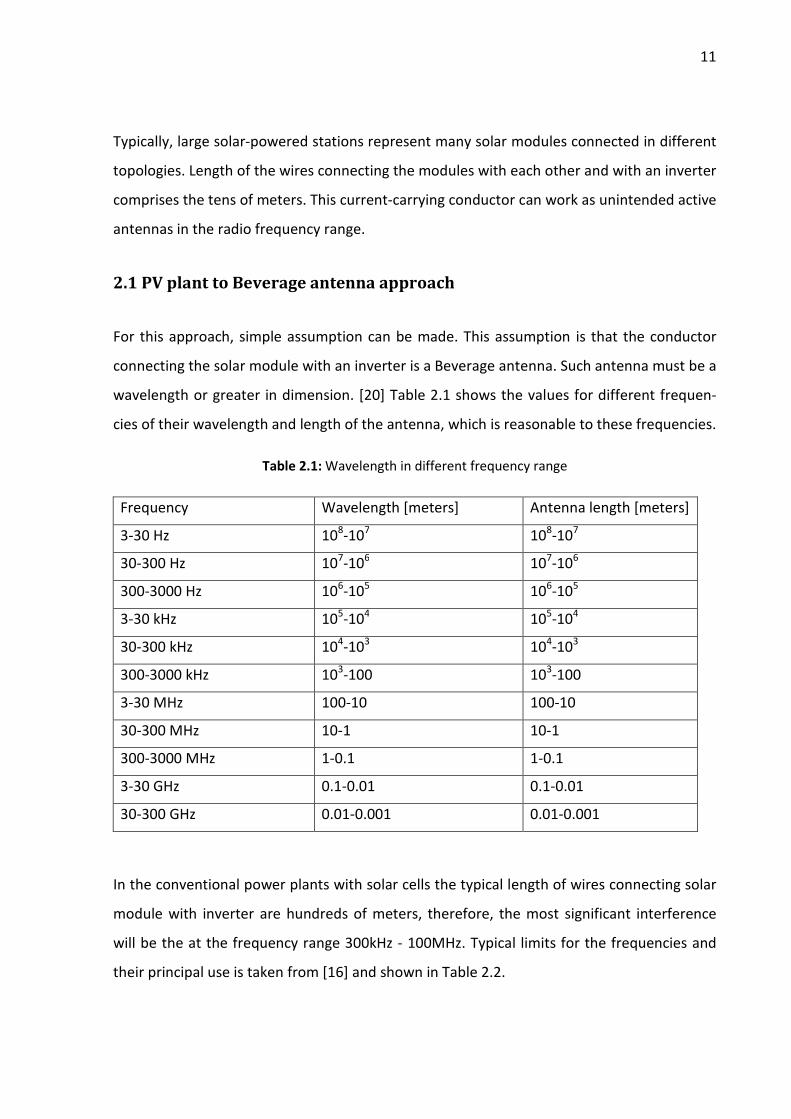
Typically, large solar-powered stations represent many solar modules connected in different
topologies. Length of the wires connecting the modules with each other and with an inverter
comprises the tens of meters. This current-carrying conductor can work as unintended active
antennas in the radio frequency range.
2.1 PV plant to Beverage antenna approach
For this approach, simple assumption can be made. This assumption is that the conductor
connecting the solar module with an inverter is a Beverage antenna. Such antenna must be a
wavelength or greater in dimension. [20] Table 2.1 shows the values for different frequen-
cies of their wavelength and length of the antenna, which is reasonable to these frequencies.
Table 2.1: Wavelength in different frequency range
Frequency Wavelength [meters] Antenna length [meters]
3-30 Hz 108-10
7 10
8-10
7
30-300 Hz 107-10
6 10
7-10
6
300-3000 Hz 106-10
5 10
6-10
5
3-30 kHz 105-10
4 10
5-10
4
30-300 kHz 104-10
3 10
4-10
3
300-3000 kHz 103-100 10
3-100
3-30 MHz 100-10 100-10
30-300 MHz 10-1 10-1
300-3000 MHz 1-0.1 1-0.1
3-30 GHz 0.1-0.01 0.1-0.01
30-300 GHz 0.01-0.001 0.01-0.001
In the conventional power plants with solar cells the typical length of wires connecting solar
module with inverter are hundreds of meters, therefore, the most significant interference
will be the at the frequency range 300kHz - 100MHz. Typical limits for the frequencies and
their principal use is taken from [16] and shown in Table 2.2.

12
Table 2.2: Principal use of different frequency range
Name Frequency Principal use
ELF (Extremely Low Frequency) 3-30 Hz
Power grids SLF (Super - Low Frequency) 30-300 Hz
ULF (Ultra - Low Frequency) 300-3000 Hz
VLF (Very – Low Frequency) 3-30 kHz Submarines
LF (Low Frequency) 30-300 kHz Beacons
MF (Medium Frequency) 300-3000 kHz AM broadcast
HF (High Frequency) 3-30 MHz Shortwave broadcast
VHF (Very High Frequency) 30-300 MHz FM,TV
UHF (Ultra High Frequency) 300-3000 MHz TV, LAN, cellular, GPS
SHF (Super High Frequency) 3-30 GHz Radar, GSO satellites, data
EHF (Extremely High Frequency) 30-300 GHz Radar, automotive, data
This simple approach shows that applications such as AM broadcast, shortwave broadcast,
FM, TV, beacons can be interferenced by disturbances produced by solar power plant. This
happens because they work in the range of frequencies 300kHz - 100MHz. Interferences in-
fluencing shortwave broadcast and beacons look particularly dangerous because they are
used to communicate with merchant ships and aircraft.
Of course, these obstacles are not dangerous if solar power plants are in the rural locality,
but often they are close to airports or placed on the building roofs which can be dangerous.

13
3 Structure of high power photovoltaic systems
The high power photovoltaic system contains several subsystems, components and other
auxiliary. The main devices of any PV solar system in EMC point of view are:
• Inverter;
• Solar cells;
• Wires.
Solar cells are compounded in modules. These modules are grouped in arrays. DC-side of
photovoltaic power plant consists of several strings. String is solar panels connected in se-
ries. The arrays are in a PV power source side, the output of units connected with a suitable
three-phase inverter. Proper switchboards are field-installed round the PV source to allow
the parallel connection of strings and arrays. The inverters are connected together in parallel
and this structure is connected to the switchboard on AC side. Output of inverters is con-
nected to line frequency transformer. PV systems are usually equipped with additional auxil-
iary such as security purpose devices and other equipment.
As example of structure Molfetta high power photovoltaic plant can be shown: “A simplified
one-line diagram of the PV system of Molfetta is shown in Fig. 3.1. It is composed of 4704
polycrystalline panels grouped in four PV subsources: the first subgenerator consists of 1184
SEM (Solar Energy Module) of 210 Wpeak, the second one of 1168 SEM of 205 Wpeak, the third
one of 1200 SEM of 220 Wpeak, and the fourth one is composed of 448 SEM of 210 Wpeak and
688 SEM of 215 Wpeak. The total rated power of the PV system is 99 804 kWpeak. The modules
are aggregated in strings composed of 16 series-connected panels, so that the total number
of strings is 294. The PV system extends over two hectares, and is isolated from the ground.
The DC voltage level of the PV source is 600V. The four inverters are SunWay TG290 of
Elettronica Santerno, with maximum input power of 286 kWpeak. The output RMS AC voltage
of the inverters is 202V. The four inverters are parallel-connected on the AC side on an ap-
propriate low-voltage (LV) switchboard at 202V, and an LV/medium voltage (MV) 202 V/20
kV power transformer is used to deliver the produced power to the network. An LV trans-
former is then used to feed the auxiliary services of the plant.”[1]

14
Figure 3.1: Simplified diagram of high power PV solar plant in Molfetta, Italy

15
3.1 PV DC-Side
DC-side of photovoltaic solar plant can be a significant source of electromagnetic (EM) emis-
sions. Electromagnetic interference (EMI) assessment of solar plant is a very difficult task.
First, equivalent circuit with parasitic elements of PV-plant should be shown. This circuit
helps to show at what places problems are. The second part of this part is DC-side to anten-
na approach. This approach can be used for numerical simulations of PV-plant.
3.1.1 Parasitic elements on DC-side
In EMC point of view RF behavior of DC side of a photovoltaic system mainly depends on two
factors:
• Capacitance between generator and earth;
• DC cable inductance.
On Fig. 3.2 the equivalent circuit of a PV panel is shown. This equivalent scheme is composed
of a connection of a current source, a capacitance, a parallel and a series resistance and two
diodes [6].
PV solar plant is a large area covered by solar modules; therefore, it represents a capaci-
tance toward the earth or, “earth capacitance”. This capacitance usually depends on several
factors:
• The size of the module;
• The height above the ground;
• The relative humidity.[1]
Typical values of capacitance have been presented in work [1] and for large ungrounded sys-
tem are shown in table 3.1

16
Table 3.1: Relative earth capacitance of solar modules for ungrounded systems [1]
Type Capacitance
Glass-faced modules 50 - 150 nF/kWpeak
Thin-film modules Up to 1 μF/kWpeak (damp environments or rainy days)
The size of large PV systems is very big (may extend over some hectares). Therefore, DC lines
may extend in length up to 150m. Long lines increase the distributed transversal capacitance
effect. This capacitance typically gives a way for CM leakage currents. [1]
Figure 3.2: Equivalent circuit of high-power solar plant in EMC point of view [1]
Grounding of the solar modules’ frames is a very interesting question because it affects not
only in EMC aspects but also it influences personnel protection and property protection.
Grounding of all commercial PV modules is allowed because it typically helps to ensure sys-
tem safety during the entire life of the plant (more than 25 years), although all industrial PV
modules are made with hardened insulation (class II components). [1]
In the U.S., grounding of DC-circuit is a very common practice because the National Electric
Code (Section 690) [7] recommends it. In Europe, the common practice is to operate the PV
generator ungrounded. [1]
The grounding of the module’s frames can significantly exert the CM impedance. At frequen-
cies below 1 MHz, grounding leads to a significant reduction of the CM impedance [1]. “It

17
reduces the common mode impedance by a factor between 2 and 3 (regardless at which lo-
cation grounding was made).” [8]
Another interesting question is the grounding of DC main cable. “A shielding of the DC main
cable may reduce electromagnetic fields significantly (at one PV site up to 50 dB!), but only
in case that the shield is grounded on both sides with (from an RF point of view) a very good
connection to earth. Also, shielded DC main cables grounded on both sides are the best
choice for optimal lightning protection.” [8] But this type of cable is not commonly used be-
cause of increased cost.
In DC cabling point of view, cabling length affects not only the distributed transversal capaci-
tance. In real case, cabling is also distributed longitudinal inductance. This inductance is a
part of a resonant circuit. Furthermore, as we know in high power solar plants the cabling
length is between 10 – 200 meters therefore wires can be in resonance for frequencies in
30 MHz – 300 kHz. Multiconductor transmission line model on Fig. 3.2 is taken from [9]. Be-
cause the PV generator can work like antenna, RF emissions appropriate to CM currents may
be significant, particularly close to probable resonant frequencies of the CM circuit.[1]
Therefore, radiated fields produced by DC side might be taken into account especially in case
of high power plants.
3.1.2 DC-side to antenna approach
There are two types of disturbances in system: common mode disturbance and differential
mode disturbance. Differential mode disturbances cause RF currents in an antiparallel way;
common mode disturbance cause disturbances in a parallel way. Therefore, two types of un-
intended antennas are presented in power plant [4]:
• Beverage antenna (common mode disturbance);
• Loop antenna (differential mode disturbance).
Simplified diagrams of antennas are shown on Fig. 3.3 and 3.4.

18
Figure 3.3: PV-plant to antenna approach (Differential mode)
Figure 3.4: PV-plant to antenna approach (Common mode)
To show how current flows through solar modules equivalent circuit for solar cell should be
shown.
Equivalent circuit of cell
To simulate work of solar plant (especially for determining magnetic fields produced by dif-
ferential mode voltages of photovoltaic power plant) the equivalent circuit of solar cell is
necessary.
Equivalent circuit for c-Si cell is shown on Fig. 3.5. [4]

19
Figure 3.5: Equivalent circuit of c-Si solar cell
The values of equivalent scheme’s resistors and capacitors are depending on the parameters
of cell. Inductance L primarily is determined by the geometry of cell connection. The imped-
ance of RC element Rdiff||Ctotal depends on many factors. These factors are:
• Cell’s bias voltage;
• Irradiation;
• Temperature;
• Frequency. [4]
For 100 cm2-cell the series resistor is constant and typically about 10mOhm. For bias voltag-
es between 350-450mV, irradiation between 500 -1000 W/m2, frequency around 100kHz
and temperature between 30-75 oC values of Ctotal and Rdiff are shown in table 3.2.
Table 3.2: Equivalent circuit values for s-Ci solar cell [4]
f=100kHz
Ctotal 10uF
Rdiff 10..400mOhm
Impedance of R||C element decreases as frequency increases. Therefore, in frequency range
150kHz – 30MHz only series resistance and inductance might be taking into account. [4]
Equivalent circuit of solar cell for this frequency range is shown on Fig. 3.6.

20
Figure 3.6: Equivalent circuit for c-Si solar cell for 150 kHz-30 MHz frequency range
In the case of simulation, equivalent circuit is shown on Fig. 3.7. These schemes are suitable
for simulations only on frequencies higher than 150 kHz. For common mode disturbances
loop is formed by parasitic earth capacitances. These capacitances are: from wires to ground
and from modules to ground. Differential mode loop is formed by series resistances of solar
cells.
Figure 3.7: Connection scheme for “plant as antenna” simulation. (a) – common mode; (b) – differen-
tial mode.

21
3.2 Inverters
Any PV generator produces DC on its output, but the public mains is AC-grid. The tasks of
inverter are to invert direct current DC into alternating current AC and to control the output
voltage. Very important feature of inverter in EMC point of view is harmonics produced by
inverter - the lower the harmonics, the better inverter.
The inverter contains several components: input filter on DC-side, DC-DC converter for
boost-up or step-down voltage produced by PV generator, full-bridge inverter and output
filter. In common PV inverters single-stage topology are quite often used. [1]
Switching frequencies of inverters are usually more than 1 kHz. Therefore, power semicon-
ductor switches are used, for example, metal–oxide–semiconductor field-effect transistors
(MOSFETs), bipolar junction transistors (BJTs) or insulated gate bipolar transistors (IGBTs).
[12]
Inverters can be divided into groups by topology (i.e.):
• Half-bridge inverters;
• Full-bridge inverters.
By number of phases:
• Single-phase;
• Three-phase.
Finally, by modulation type:
• PWM (Pulse width modulation) inverters;
• Square wave and trapezoidal inverters.
Spectrum of higher harmonics (in radio frequency) produced by inverter is very important in
RF interference point of view. This spectrum depends on topology and modulation type. [5]

22
3.2.1 Inverter topologies
There are many types of inverters based on different circuits. Three-phase inverters are usu-
ally based on full bridge topology. [12]
Half-bridge inverter. Simplified schematic of half bridge inverter is shown on Fig. 3.8. This is
the one of the simplest topologies of inverters. Power switches S1 and S2 work in antiphase.
Two equal capacitors are connected in series to create a point with a midpotential equal to
half of input voltage.
Figure 3.8: Simplified circuit of half-bridge inverter
Full-bridge inverter. Simplified schematic of full bridge inverter is shown on Fig. 3.9. This to-
pology has two pair of power switches. Each pair works in antiphase. Although the voltage
and current through the switches the same as for half-bridge inverter, output power is two
much higher. At high-power levels, this is distinct advantage. [5]

23
Figure 3.9: Simplified circuit of full-bridge inverter
Three-phase inverter. Simplified circuit of three-phase inverter is shown on Fig. 3.10. This is
most frequently used circuit for three-phase applications. [5]
Figure 3.10: Simplified circuit of three-phase full-bridge inverter
3.2.2 Modulation types
Sine-triangle PWM has been a very popular type of modulation. This method is relatively un-
sophisticated. [21] The idea of this modulation is to shape and control the three-phase out-
put voltages in magnitude and frequency with a constant input voltage. [5] However, this

24
method is unable to make full use of the inverter’s supply voltage and the asymmetrical na-
ture of the PWM switching characteristics produces relatively high harmonic distortion in the
supply. Space Vector PWM (SVPWM) is a more sophisticated technique for generating a fun-
damental sine wave that provides a higher voltage to the load and lower total harmonic dis-
tortion. [21]
The switching frequency of semiconductor device in PWM can be more than 16kHz. [1]
Without appropriate disturbance cancellation higher harmonic bandwidth can reach tens
MHz. Another source of disturbances is non-zero switch-on/switch-off time of semiconduc-
tor device.
In example to obtain values of higher harmonics for sine-triangle modulation, amplitude
modulation ratio ma and frequency modulation ratio mf can be used. These values can be
calculated by using equations 3.1 [5] and 3.2 [5] respectively.
tri
control
s UUm = (3.1)
ff
m1
s
f= (3.2)
Where f1 for typical photovoltaic applications is 50Hz or 60Hz; fs is a switching frequency of
semiconductor device; Ucontrol is a peak value for control signal; Utri is a peak value of triangle
signal.
Values for higher harmonics can be obtained approximately by table 3.3. This table is taken
from [5].

25
Table 3.3: Higher harmonics values
ma
h.n.
0.2 0.4 0.6 0.8 1
1 0.2 0.4 0.6 0.8 1
mf 1.242 1.15 1.006 0.818 0.601
mf±2 0.016 0.061 0.131 0.220 0.318
mf±4 - - - - 0.018
2∙mf±1 0.190 0.326 0.370 0.314 0.181
2∙mf±3 - 0.024 0.071 0.139 0.212
2∙mf±5 - - - 0.013 0.033
3∙mf 0.335 0.123 0.083 0.171 0.113
3∙mf±2 0.044 0.139 0.203 0.176 0.062
3∙mf±4 - 0.012 0.047 0.104 0.157
3∙mf±6 - - - 0.016 0.044
4∙mf±1 0.163 0.157 0.008 0.105 0.068
4∙mf±3 0.012 0.07 0.132 0.115 0.009
4∙mf±5 - - 0.034 0.051 0.119
4∙mf±7 - - - 0.017 0.05
The other way to obtain higher harmonics value is to simulate the operation of inverter in
SPICE (Simulation Program with Integrated Circuit Emphasis) software. The most accurate
way is to measure disturbance voltages on existing inverter. For this purposes line imped-
ance stabilization networks (LISN) can be used. [18] LISNs are described in part 5.1.
3.2.3 Examples
Inverters produce disturbances. Bandwidth of these disturbances depend on several factors
such as switching frequency, modulation type and turn-on / turn-off time of semiconductor
switch. In this part, comparison between several types of switching schemes is shown. All
schemes in this chapter are simulated using Simulink SimPowerSystems library.
Simulink model for simulations is shown on Fig. 3.11. In this model, three-phase full-bridge
inverter is used. Control signals are made by pulse generator module. Sine-triangle method
is used. Output current is fully smoothed.

26
Figure 3.11: Model of three-phase inverter in Simulink
PWM inverter linear modulation
First example is inverter in linear modulation mode. ma = 0.6; fsw = 5kHz. Fig. 3.12, 3.13, 3.14
show output voltage between phases, current in DC-lines and harmonics spectrum respec-
tively.
0.458 0.46 0.462 0.464 0.466 0.468 0.47 0.472 0.474 0.476 0.478
-400
-200
0
200
400
Time (s)
Uab
(V
)
Figure 3.12: Inverter output voltage between phases A and B (linear modulation)

27
0.456 0.457 0.458 0.459 0.46 0.461 0.462 0.463 0.464 0.4650
10
20
30
40
50
60
70
Time (s)
I (A
)
Figure 3.13: Current in DC lines (linear modulation)
Figure 3.14: Harmonics spectrum in DC-lines current (linear modulation)
50 Hz frequency is used as basic for fast Fourier transform (FFT). In frequency range be-
tween 80kHz – 95kHz the maximum value of distortion current is near 5 percent of DC value.
PWM overmodulation
ma= 1.15; fsw = 5kHz. Overmodulation is intermediate step between linear modulation and
square wave modulation. Fig. 3.16, 3.17, 3.18 show output voltage between phases, current
in DC-lines and harmonics spectrum respectively.

28
0.44 0.445 0.45 0.455-400
-300
-200
-100
0
100
200
300
400
Time (s)
Vab
(V)
Figure 3.15: Inverter output voltage between phases A and B (overmodulation)
0.448 0.449 0.45 0.451 0.452 0.453 0.454 0.455 0.4560
20
40
60
80
100
120
Time (s)
Cur
rent
(A
)
Figure 3.16: Current in DC lines (overmodulation)

29
Figure 3.17: Harmonics spectrum in DC-lines current (overmodulation)
In frequency range between 90kHz – 100kHz the maximum value of distortion current is less
than 2 percent of DC value.
Input filter influence
To show input filter influence, filter should be added to model presented on Fig 3.11. Model
with simple input filter is shown on Fig. 3.18. Calculation of filter parameters is not objective
of this thesis. Therefore, these parameters are taken quite big. Capacitances are 100uF and
inductance is 100mH.
Figure 3.18: Simulink model of three-phase inverter with input filter

30
DC-side current waveform is shown on Fig. 3.19.
0.54 0.55 0.56 0.57 0.58 0.59 0.6 0.61 0.629.2
9.25
9.3
9.35
9.4
9.45
9.5
9.55
9.6
Time (s)
Cur
rent
(I)
Figure 3.19: DC-side current waveform
Fast Fourier transform for DC – side current is shown on Fig. 3.20.
Figure 3.20: Fast Fourier transform for DC-side current.
Fig. 3.20 shows that in frequency range between 90 – 100 kHz the maximum value of distor-
tion current in DC-side is less than 10-6
%.
These simulation shows that input filter can significantly reduce value of distortion currents
in DC lines.

31
3.3 Summary of plant structure
This chapter shows that EMC of high-power solar plant depends on several factors such as:
equipment used in solar plant (inverters, wires, cells, etc.) and construction of solar plant
(i.e. grounding).
One of the main questions in this work is “Are RF disturbances produced by high power PV
solar plant significant?” The answer for this question can be given by Fig. 3.21
Figure 3.21: Antenna factor of a PV generator (24 modules in series 1m height 7.5m cable
length) [13]
Fig. 3.21 shows the measured CM and DM antenna factor of a PV generator (24 modules in
series 1m height 7.5m cable length). Common mode disturbance has a pronounced reso-
nance at 1MHz with value of -65dB S/m. The antenna factor of half-wave dipole antenna in
free space at measuring distance of 3m is -60 dB S/m therefore RF disturbances produced by
high power PV solar plant can be significant. [13] The other measurements of PV plant AF
are given in the chapter 6.

32
4 Current standards for PV applications
At present, international standards for the conducted RF emissions of the inverters for do-
mestic and industrial environments exist only for the maximum levels on the AC-side. For the
DC-side, international standards are not available. Nevertheless, during project ESDEPS [10]
possible limits have been tested and proposed. The common approach is to use AC-side RF
limits on DC-side. [1]
For maximum magnetic field strength, the limits can be given by the VDE 0878-1 (Fig. 4.1).
These limits are recommended for installations and for systems by the German authori-
ties. [2]
Figure 4.1: Magnetic field strength limits given by VDE 0878-1 (distance – 3m) [4]
RF-voltage limits for emissions on the DC-side. Based on the emission measurements and the
simulations made during the project [10] the following recommendations can be given for
the voltage limits:
“For conducted RF voltages on the DC side, the limits should be between the AC and the DC
limits of EN 55014-1 [14] (Fig. 4.2). Inverters meeting these limits are likely not to cause

33
harmful interference in practical operation. Their emitted field disturbances will be clearly
lower than those specified in VDE 0878-1.” [4]
Figure 4.2: Limits for disturbance voltages [4]

34
5 Emission tests
Measurements are important part of solar power plant assessment in EMC point of view.
Measurements should be divided into two parts:
• Measurement of common mode voltages and disturbance mode voltages produced
by inverter;
• Measurements of EM field.
Both of the measurements are important for EMC assessment.
5.1 Measurement of CM and DM voltages produced by inverter
Measurement of conducted RF emissions at a defined terminating network (LISN) is a good
method. It simplifies EMC assessment.
For this purposes HTA Burgdorf and Schaffner AG [17] have realized a quite simple DC-LISN
with ZCM = 150 Ohm and used it for RF measurements on the DC-side. This DC-LISN is shown
on Fig. 5.1. Impedance ZCM of LISN is shown in Fig. 5.2. [17]
Figure 5.1: Schematic diagram of DC-LISN ZCM=150 Ohm according to EN61000-4-6 [17]

35
Figure 5.2: Impedance and phase of DC-LISN [17]
During the project PV-EMI [10] extending measurements of impedance values, antenna fac-
tors and radiated electromagnetic fields of real PV generators were made.
Following values for impedances were agreed during this project:
• Common mode ZCM = 250 Ohm (+100%,-50%);
• Differential mode ZDM = 100 Ohm (+100%,-50%).
Limits for RF voltages at a DC-LISN with the impedance values given above:
• 150 kHz < f < 500 kHz : 80 dBuV quasi-peak;
• 500 kHz < f < 30 MHz : 64 dBuV quasi-peak.
In the summer 2000 realization of new DC-LISN was started. [17] Different versions of this
DC-LISN were realized and tested. As result new DC-LISN for 1kV 75A was made. This LISN is
shown on Fig. 5.3. Common mode impedance is shown on Fig. 5.4, differential mode imped-
ance is shown on Fig. 5.5. [17]

36
Figure 5.3: Schematic diagram of DC-LISN [17]
Figure 5.4: Measured common mode impedances [17]

37
Figure 5.5: Impedance and phase of DC-LISN [17]
Measurement of RF voltages at DC-LISN can ensure EMC of PV equipment on the DC-side.
This method looks simpler because only one installation with LISN and PV-array simulator
can be used to test many inverters.

38
5.2 Measurement of radiated field
To assess the value of radiated field the antenna factor value is used. EMC and RF engineers
use Antenna factor to obtain value of radiated electromagnetic field. Perhaps, antenna fac-
tor is the most commonly used value to show radiated field in EMC point of view. [11]
For electric field antenna factor is calculated as (5.1) [11]
[1/m] received
incident
electric
VEAF = (5.1)
For magnetic field antenna factor is calculated as (5.2) [11]
[S/m] received
incident
magnetic
VHAF = (5.2)
Antenna factor acts like a transfer function. In other words, the higher the antenna factor
the higher is the generated field with a certain feeding voltage. Antenna factor can be
whether complex or real. In the case of complex antenna factor the phase and amplitude
information can be derived from antenna factor, but in real cases only magnitude of antenna
factor is used. [11]
Units of Antenna factor. Decibel is a logarifmic value equal to )log(20 BA = . It is usually
used for dimensionless values, such as amplifier gain or antenna gain. However, antenna fac-
tor is not dimensionless value.
For electric field antenna factor dimension is 1/m, for magnetic field antenna factor dimen-
sion is S/m. Therefore, in case of log scale initial antenna factor is divided by antenna factor
of 1 V/m or 1/m.
For example, antenna with a given electric field antenna factor of 6 dB will create an output
voltage of 0.5V for an in incident field of 1 V/m. Sometimes this antenna factor can be writ-
ten as 6 dB 1/m, but also it can be written as 6dB/m. [11]

39
Antenna factor measurement. To measure antenna factor of photovoltaic system, the dis-
turbance voltage (in common or in differential mode) should be injected in the DC-lines of
generator. To calculate antenna factor magnetic field at 3m distance and RF voltage should
be measured. After that, antenna factor can be calculated using these values.
Test setup for antenna factor and impedance measurements is shown on Fig 5.6. “A current
probe is used to inject RF signals generated with tracking generator and amplifier into the PV
generator. The amplitude of the injected current is measured with a second probe together
with the radiated magnetic field. A mesh in front of the PV generator serves as reference
ground.
EMC-spectrum analyzer HP8591 EM in combination with two broadband antennas (an active
loop antenna for the frequency range of 150 kHz to 30 MHz and a biconical antenna for the
frequency range between 30 MHz and 300 MHz) and a RF-current probe was used to per-
form the tests.”[10]
Figure 5.6: Test setup for impedance and antenna factor measurements.
Two current probes are injected and they measure RF currents (common and differential
mode is provided). The radiated electromagnetic field is measured with two antennas (an
active loop antenna and a biconical) according to the appropriate frequency range. [10]

40
6 Existing Measurements
Measurement part is divided into two subparts. First part represents measurements at the
ISET experimental system. Using this installation, measurements of magnetic field and dis-
turbance voltages were made for different types of solar modules connection.
At the second part DC-side of high-power solar plant at Molfetta, Italy is shown in EMC point
of view.
6.1 Measurements at the ISET experimental system [10]
Through the project [10] ISET built several experimental PV systems in order to study the
properties of complete PV systems and perform EMC specific investigations. During the pro-
ject installation was enlarged from 8 PV modules to 16 and finally to 24 modules. Module is
55 Wpeak. [10]
The electrical output of the generator used is about 1.3 kWpeak. The system is fully adjusta-
ble. Height of installation, connection to ground, and modules’ connection to each other can
be customized.
This system was used for measurements of antenna factor and impedance of the PV-
generator as shown in the section 5.2. During installation operation, magnetic field and dis-
turbance currents were measured.
Connection’s influence. At Fig. 6.1 and 6.2 the measured common mode and differential
mode antenna factors are shown. Common mode antenna factor for grounded system can
reach -55 dB. It is more than for the other types of connections. This measurement can
prove the fact from chapter 3. The emissions produced by PV power plant can be significant
and grounding can decrease CM impedance of the system (at the lower frequencies). There-
fore, AF for CM disturbances increases.

41
Figure 6.1: Measured CM antenna factors for different configurations of a PV generator [10]
Figure 6.2: Measured DM antenna factors for different configurations of a PV generator [10]

42
Inverter’s influence. On Fig. 6.3 and 6.4 disturbance currents and radiated magnetic fields are
shown. These inverters are commercially available on the market. The first inverter produces
disturbance currents that lead to significant electromagnetic field. The VDE 0878-1 standard
is exceeded in wide bandwidth. However, current disturbances produced by the second in-
verter are not as high as by first inverter. Therefore, radiated magnetic field of the second
inverter maintains VDE 0878-1 standard. [10]
Figure 6.3: Disturbance current and magnetic field strength for first inverter [10]
Figure 6.4: Disturbance current and magnetic field strength for second inverter [10]

43
Disturbances at high frequencies. Nevertheless, radio distortions may occur not only at fre-
quencies lower than 30MHz. In some cases, the actual limits may be exceeded significantly.
“A good correlation between the on-site measurement of the radiated electric field and ra-
dio frequency power measurement in the lab can be shown” (see Fig. 6.5) [10].
Figure 6.5: RF power measured in the lab and electric field measured at a PV generator operated
with a commercially available inverter [10]
44
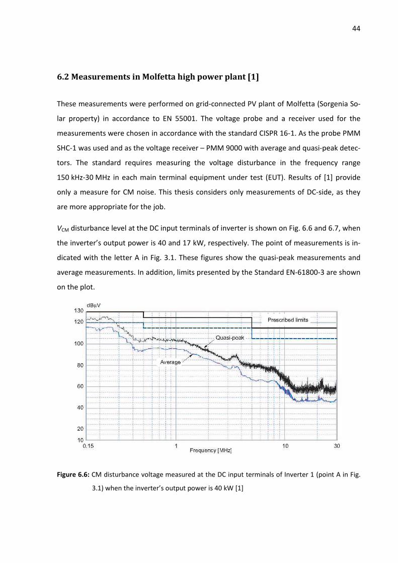
6.2 Measurements in Molfetta high power plant [1]
These measurements were performed on grid-connected PV plant of Molfetta (Sorgenia So-
lar property) in accordance to EN 55001. The voltage probe and a receiver used for the
measurements were chosen in accordance with the standard CISPR 16-1. As the probe PMM
SHC-1 was used and as the voltage receiver – PMM 9000 with average and quasi-peak detec-
tors. The standard requires measuring the voltage disturbance in the frequency range
150 kHz-30 MHz in each main terminal equipment under test (EUT). Results of [1] provide
only a measure for CM noise. This thesis considers only measurements of DC-side, as they
are more appropriate for the job.
VCM disturbance level at the DC input terminals of inverter is shown on Fig. 6.6 and 6.7, when
the inverter’s output power is 40 and 17 kW, respectively. The point of measurements is in-
dicated with the letter A in Fig. 3.1. These figures show the quasi-peak measurements and
average measurements. In addition, limits presented by the Standard EN-61800-3 are shown
on the plot.
Figure 6.6: CM disturbance voltage measured at the DC input terminals of Inverter 1 (point A in Fig.
3.1) when the inverter’s output power is 40 kW [1]

45
Figure 6.7: CM disturbance voltage measured at the DC input terminals of Inverter1 (point A in Fig.
3.1) when the inverter’s output power is 17 kW [1]
Moreover, Fig. 6.6 and 6.7 show that disturbance voltages do not depend on output power.
If disturbance voltages exceed EN-61800-3 limits, especially on the lower frequency range,
they will be the cause of incorrect work of electronic devices. [1]
Another very important fact is that filters are connected in parallel between the positive and
negative conductors, and ground at the DC input port of the inverter significantly decreases
disturbance level especially in low-frequency range (below 1 MHz) [1]. Measured common
mode disturbance voltages (with Enerdoor filters connected in parallel) is shown on Fig. 6.8.

46
Figure 6.8: The effect of Enerdoor filters connected in parallel between the positive and negative
conductors and ground [1]
Also, during the work [1] measurements of common mode voltages VCM at the DC output
terminals of a panelboard (point B Fig. 3.1) were made. VCM has been measured for better
insight to the CM disturbance behavior. Values of frequency range between 9 to 150 kHz are
shown on Fig. 6.9; Fig. 6.10 shows VCM values for 150 kHz to 30 MHz range. The figures verify
the assumption that the conducted disturbances propagate along the DC cabling. [1]

47
Figure 6.9: CM disturbance voltage measured at the DC output terminals (9 kHz – 150 kHz)
(point B Fig. 3.1) [1]
Figure 6.10: CM disturbance voltage measured at the DC output terminals (150 kHz – 30 MHz) (point
B Fig. 3.1) [1]

48
The last measurement for DC-side is shown on Fig. 6.11. “This last measurement confirms
that the CM disturbances delivered by the inverter, after propagating across the DC and AC
side of the PV system, couple again through the ground connections (paths A and B in
Fig. 3.1).” For this experiment, VCM has been measured at the point C on Fig. 3.1. [1]
Figure 6.11: CM disturbance voltage measured at the ground connection of inverter n 1, (point C in
Fig. 3.1) [1]

49
6.3 Analyzing of the measurements
Gathering the data and measurements made during the projects [1] [10] and [8], the follow-
ing conclusions can be made.
6.3.1 Equipment influence
Components used for solar plant creation can influence EMC of system:
• Solar module construction. Solar module construction can significantly affect pro-
duced disturbances. Aluminum foil on the modules’ backside reduces the differential
mode antenna factor by 20 - 30 dB. Frame reduces antenna factor only by 10 dB. [8]
• Cabling. A shielding of the DC main cable may reduce electromagnetic fields signifi-
cantly (at one PV site up to 50 dB!), but only in case the shield is grounded on both
sides with (from an RF point of view) a very good connection to earth. [8]
• Inverter. Inverter is a source of high frequency disturbances. Only tested PV inverters
(with low distortion currents) can be used in photovoltaic solar plants. [8]
• DC-filter. Input DC-filter can reduce common mode distortion voltage significantly (by
40 dBuV) [1].
6.3.2 Solar plant’s structure influence
For common mode disturbances these factors are:
• Grounding. The common mode impedance strongly depends on the grounding of
frames. Grounding of frames is very common, but a connection to earth reduces the
common mode impedance two or three times (depend on grounding location). [8]
• Height of the system. The common mode antenna factor strongly depends on the PV
generator height from the ground. The higher system is the bigger antenna factor
is. [8]

50
For differential mode the most significant factor is the type of PV system (number of strings
in parallel and number of modules in series). [8]
Although system grounding reduces common mode impedance (especially at the lower fre-
quencies), this step helps to obtain stable value of CM impedance. Therefore, dangerous of
resonant effects can be reduced significantly. In addition, fluctuations of CM impedance can
be decreased by bonding of PV modules frames. [1]
51
7 Simulations
Disturbances produced by power plant depend on several factors. For RF disturbances on
DC-side the most important factors are:
• Number of modules;
• Type of modules connection (number of element in parallel and series);
• Height of the system;
• Distance between PV-generator and inverter;
• Frame occurrence;
• Type of grounding;
• Cell’s connection in modules.
Target of these simulations is to show how some of this factors change antenna gain of PV-
array.
To obtain antenna values the Maxwell equations must be solved. There are several numeri-
cal methods for this, but in this work MMANA-GAL software is used. MMANA-GAL is very
simple software which was made for antenna calculation. It uses “method of moments” for
Maxwell equation solving. In this work calculation of isotropic gain is used.
Target of these simulations is to obtain how DC-side isotropic gain depends on several fac-
tors:
• Solar array structure;
• Distance between wires;
• Solar module structure.
All simulations are made for both CM and DM disturbances. It is worth noting that these
simulations are made for qualitative assessment of these factors.

52
7.1 Simulation of different structures
In the first part two types of solar module connections are simulated. The first type of con-
nection is 12 modules inline and the second is array of 3x4 modules. In theory connection
type should significantly affect the differential mode antenna gain because AC loop depends
on connection type.
Size of one solar module is 1m x 1m. Simulations are made for differential mode and dis-
turbance mode voltages. The frequencies are between 0.3 MHz and 30 kHz. Height from
ground is 5 meters.
7.1.1 Simulation 1 “12 modules inline”
In this simulation 12 modules of solar plant are connected inline. Therefore, this type of
connection should create big loop in comparison with the same amount of modules con-
nected in array. MMANA model for this case is shown on Fig. 7.1.
Figure 7.1: MMANA model used for 12 modules inline simulation
Simulation results are shown in table 7.1.

53
Table 7.1: Simulation results for 12 modules inline structure of plant
G, dBi
f, MHz CM DM
0,3 -17,83 -15,44
0,4 -13,9 -10,93
0,5 -17,56 -14,37
0,6 -15,4 -11,68
0,7 -13,68 -9,44
0,8 -12,26 -7,51
0,9 -11,08 -5,82
1 -10,08 -4,33
2 -6,11 3,63
3 -11,11 5,15
4 1,82 1,99
5 7,17 8,78
6 8,04 8,38
7 8,06 7,96
8 8,81 7,58
9 6,91 7,17
10 6,83 6,54
12 6,35 6,84
15 5,43 5,86
17 5.51 5,94
20 5,69 6,95
22 7,3 5,38
25 5,92 5,87
27 5,81 6,51
30 6,76 7,18
7.1.2 Simulation 2 “3x4 array”
In the second simulation, 12 modules are connected in series-parallel way. In comparison
with the first case, this type of connection should decrease value of DM antenna gain. Con-
nection scheme is shown in Fig. 7.2
54
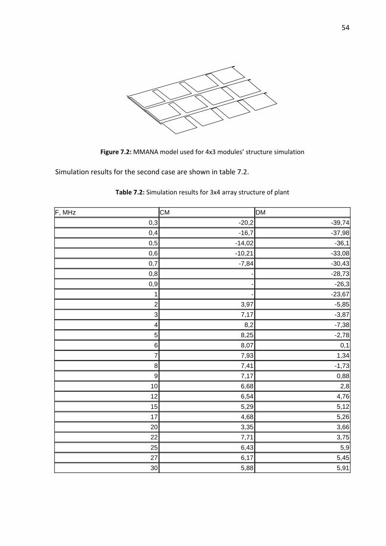
Figure 7.2: MMANA model used for 4x3 modules’ structure simulation
Simulation results for the second case are shown in table 7.2.
Table 7.2: Simulation results for 3x4 array structure of plant
F, MHz CM DM
0,3 -20,2 -39,74
0,4 -16,7 -37,98
0,5 -14,02 -36,1
0,6 -10,21 -33,08
0,7 -7,84 -30,43
0,8 - -28,73
0,9 - -26,3
1 - -23,67
2 3,97 -5,85
3 7,17 -3,87
4 8,2 -7,38
5 8,25 -2,78
6 8,07 0,1
7 7,93 1,34
8 7,41 -1,73
9 7,17 0,88
10 6,68 2,8
12 6,54 4,76
15 5,29 5,12
17 4,68 5,26
20 3,35 3,66
22 7,71 3,75
25 6,43 5,9
27 6,17 5,45
30 5,88 5,91

55
7.1.3 Comparison between two cases
Common mode. Fig. 7.3 shows isotropic gains for both cases. Red line is isotropic gain for
the first case and blue line is for second one. Antenna gain dependence of modules’ connec-
tion cannot be determined using this simulation.
100
101
-60
-50
-40
-30
-20
-10
0
10
Frequency (kHz)
Isot
ropi
c ga
in (
dBi)
Figure 7.3: Isotropic gain comparison for common mode
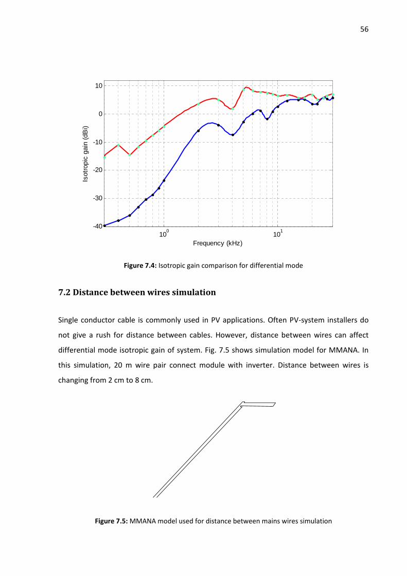
Differential mode. Theoretically, connection type should affects the differential mode an-
tenna gain. Results of this simulation (shown in Fig. 7.4. Red line – first case, blue line – se-
cond case) can prove it. Second type of connection can significantly decrease the value of
antenna gain especially on lower frequencies.
56
100
101
-40
-30
-20
-10
0
10
Frequency (kHz)
Isot
ropi
c ga
in (
dBi)
Figure 7.4: Isotropic gain comparison for differential mode
7.2 Distance between wires simulation
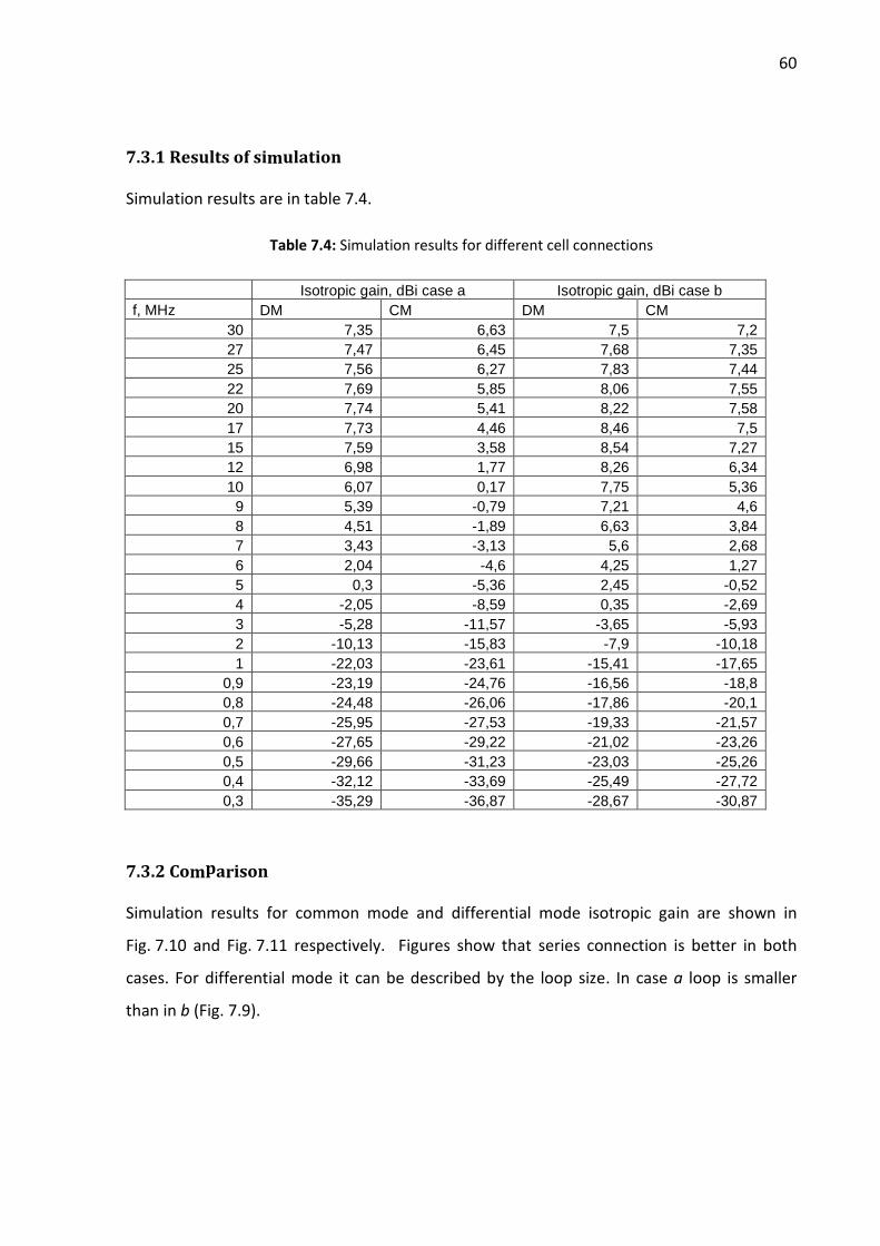
Single conductor cable is commonly used in PV applications. Often PV-system installers do
not give a rush for distance between cables. However, distance between wires can affect
differential mode isotropic gain of system. Fig. 7.5 shows simulation model for MMANA. In
this simulation, 20 m wire pair connect module with inverter. Distance between wires is
changing from 2 cm to 8 cm.
Figure 7.5: MMANA model used for distance between mains wires simulation

57
7.2.1 Simulation results
Simulation results are in table 7.3.
Table 7.3: Simulation results for different distances between wires (CM and DM)
D = 8cm D = 6cm D = 4cm D = 2cm f, MHz GDM GCM GDM GCM GDM GCM GDM GCM
30 7,23 8,79 7,23 8,5 7,22 9,4 7,2 11,78 27 6,78 -25,34 6,77 -29,8 6,76 -33,34 6,71 -8,1 25 8,64 -8,55 8,56 -11,06 8,44 -14,41 8 -20,38 22 3,8 -9,64 2,73 -12,04 1,66 -15,44 0,76 -21 20 7,5 -8,14 7,36 -10,59 7,14 -14,07 6,63 -20,16 17 6,86 -3,88 6,84 -6,16 6,81 -9,41 6,77 -13,19 15 6,39 5,91 6,38 6,67 6,37 9,71 6,38 -1,26 12 6,08 -16,08 6,07 -18,66 6,05 -21,62 5,98 -28,18 10 2,73 -27,24 2,66 -35,1 2,48 -33,03 0,98 -13,96
9 5,54 -20,77 5,24 -23,21 4,36 -26,55 -2,34 -31,48 8 -0,07 -14,6 -1,31 -16,99 -5,02 -20,14 -7,96 -25,17 7 -2,2 -16,24 -2,79 -18,58 -2,83 -21,82 -1,16 -26,23 6 3,29 -21,38 1,79 -22,63 1,21 -25,25 0,19 -31,43 5 3,12 -28,8 2,64 -30,75 1,85 -32,64 -0,09 -39,61 4 2,68 -36,42 2,02 -29,75 0,85 -40,16 -2,27 -51,06 3 0,09 -35,64 -0,85 -28,66 -2,49 -47,56 -6,5 -42,73 2 -6,72 -52,71 -7,92 -43,25 -9,91 -52,54 -14,23 -56,62 1 -21,79 -59,68 -23,09 -70,91 -25,04 -67,54 -27,97 -61,8
0,9 -24,65 -52,18 -25,94 -63,89 -27,82 -73,69 -30,41 -64,2 0,8 -27,21 -62,08 -28,47 -57,34 -30,24 -60,86 -32,48 -67,06 0,7 -30,43 -64,46 -31,65 -66,11 -33,27 -63,91 -35,13 -80 0,6 -33,46 -76,76 -34,61 -64,33 36,03 -80,26 -37,48 -73,41 0,5 -38,04 -70,47 -39,07 -78,62 -40,23 -71,6 -41,29 -80,57 0,4 -43,77 -76,83 -44,62 -88,44 -45,48 -85,33 -46,17 -83,67 0,3 -50,23 -77,3 -50,82 -81,3 -51,36 -91,18 -51,74 -89,31
7.2.2 Comparison
Measurement results for common mode and differential mode are shown in Fig. 7.6 and
Fig. 7.5 respectively. For common mode antenna, gain dependence of distance cannot be
determined. Nevertheless, for differential mode the closer wires to each other the lower DM
antenna gain.

58
100
101
-80
-60
-40
-20
0
Frequency (KHz)
Isot
ropi
c ga
in (
dBi)
Figure 7.6: Isotropic gain comparison for common mode
100
101
-50
-40
-30
-20
-10
0
10
Frequency (kHz)
Isot
ropi
c ga
in (
dBi)
Figure 7.7: Isotropic gain comparison for differential mode
It is worth noting that differential gain dependence on distance is close to hyperbolically.
(shown in Fig. 7.8). The closer wires, the lower differential mode gain.

59
2 3 4 5 6 7 8
-6
-5
-4
-3
-2
-1
0
Distance between wires (cm)
Isot
ropi
c ga
in (
dBi)
Figure 7.8: DM mode isotropic gain. (f = 3 MHz)
7.3 Module structure simulation
Solar module consists of tens of cells. Therefore, it is interesting in EMC point of view to
simulate different types of cells connection. Two cases are simulated:
• All cells in series (Fig. 7.9 a);
• Series – Parallel connection (Fig. 7.9 b).
Figure 7.9: Solar cells connection
60
7.3.1 Results of simulation
Simulation results are in table 7.4.
Table 7.4: Simulation results for different cell connections
Isotropic gain, dBi case a Isotropic gain, dBi case b f, MHz DM CM DM CM
30 7,35 6,63 7,5 7,2 27 7,47 6,45 7,68 7,35 25 7,56 6,27 7,83 7,44 22 7,69 5,85 8,06 7,55 20 7,74 5,41 8,22 7,58 17 7,73 4,46 8,46 7,5 15 7,59 3,58 8,54 7,27 12 6,98 1,77 8,26 6,34 10 6,07 0,17 7,75 5,36
9 5,39 -0,79 7,21 4,6 8 4,51 -1,89 6,63 3,84 7 3,43 -3,13 5,6 2,68 6 2,04 -4,6 4,25 1,27 5 0,3 -5,36 2,45 -0,52 4 -2,05 -8,59 0,35 -2,69 3 -5,28 -11,57 -3,65 -5,93 2 -10,13 -15,83 -7,9 -10,18 1 -22,03 -23,61 -15,41 -17,65
0,9 -23,19 -24,76 -16,56 -18,8 0,8 -24,48 -26,06 -17,86 -20,1 0,7 -25,95 -27,53 -19,33 -21,57 0,6 -27,65 -29,22 -21,02 -23,26 0,5 -29,66 -31,23 -23,03 -25,26 0,4 -32,12 -33,69 -25,49 -27,72 0,3 -35,29 -36,87 -28,67 -30,87
7.3.2 Comparison
Simulation results for common mode and differential mode isotropic gain are shown in
Fig. 7.10 and Fig. 7.11 respectively. Figures show that series connection is better in both
cases. For differential mode it can be described by the loop size. In case a loop is smaller
than in b (Fig. 7.9).

61
100
101
-35
-30
-25
-20
-15
-10
-5
0
5
Frequency (kHz)
Isot
ropi
c ga
in (
dBi)
Figure 7.10: Isotropic gain of solar module (CM) (red – a, blue – b)
100
101
-35
-30
-25
-20
-15
-10
-5
0
5
10
Frequency (kHz)
Isot
ropi
c ga
in (
dBi)
Figure 7.11: Isotropic gain of solar module (DM) (blue – a, red – b)

62
7.4 Simulation results
According to the simulation results, the following conclusions can be made:
• Modules’ connection influence DM antenna gain. Array structure of plant is bet-
ter (Fig. 7.2);
• Distance between wires affects DM antenna gain. Wires should be installed as close
as possible;
• Cells connection exerts both types of gains. Series connection of cells is better.

63
8 Conclusion
Target of this work is to answer for three questions:
• “Are RF disturbances produced by high-power photovoltaic plant significant?”
• “Who made researches on this topic?”
• “What can we do to prevent emissions?”
Not only high-power, but also any photovoltaic solar plant can produce significant RF dis-
turbances. This can be proved by works “EMC and safety design for photovoltaic systems
(ESDEPS)” and “EMC Issues in High-Power Grid-Connected Photovoltaic Plants”.
To reduce disturbances following actions should be made:
• Using solar modules with frame and foil on the backside;
• Using a shielded DC cable with both sides grounding;
• Attention to the cable installing (cables should be placed as close as possible);
• Using inverter with low DC-side distortion current;
• Using DC-side filter;
• Attention to plant structure.
The most interesting question is the grounding of PV-system. At one hand it decreases CM
impedance. At the other hand it provides system protection and helps to obtain stable value
of CM impedance. The author’s opinion is that grounding is necessary, because in this case
dangerous resonant effects can be reduced.

64
References
[1] Rodolfo Araneo, Sergio Lammens, Marco Grossi, and Stefano Bertone, “EMC Issues
in High-Power Grid-Connected Photovoltaic Plants,” IEEE transactions of electro-
magnetic compatibility, vol. 51, no.3, aug. 2009
[2] S. Schattner, G. Bopp, T. Erge, R. Fischer, H. Haeberlin, R. Minkner, R. Venhuizen,
and B. Verhoeven, “Development of standard test procedures for electromagnetic
interference (EMI) tests and evaluations on photovoltaic components and plants -
PV-EMI,” Publishable Final Rep. EU Project number JOR3-CT98-0217
[3] C. Bendel, T. Degner, J. Kirchhof, G. Klein, H. Lange, C. Trousseau, A. Schulbe, C. Hal-
ter, C. Metzger, H. Daub, K. Stanley, N. Henze, P. Claus, P. Scheibenreiter, P. Wurm,
and W. Enders, “EMC and safety design for photovoltaic systems (ESDEPS),” Publish-
able Final Rep. EU Pro-ject number JOR3-CT98-0246
[4] S. Schattner, G. Bopp, T. Erge, R. Fisher, H. Haeberlin, R. Minker, R. Venhuizen, B.
Verhoeven, ”A new measurement technique ensuring the EMC of photovoltaic sys-
tems”. Proc. 14th EMC Zurich Symposium, 2001
[5] N. Mohan, T. M. Undeland, and W. P. Robbins, “Power Electronics”. New York:
Wiley, 1995
[6] J. A. Mazer, Solar Cells, “An Introduction to Crystalline Photovoltaic Tecnology.” Nor-
well, MA: Kluwer, 1997
[7] “NFPA 70: National Electric Code,” Nat. Fire Protection Assoc. (NFPA), Quincy, MA,
2008
[8] S. Schattner, G. Bopp, T. Erge, R. Fischer, H. Häberlin, R. Minkner, R. Venhuizen, B.
Verhoeven “PV-EMI” – developing standard test procedures for the electromagnetic
compatibility (EMC) of PV components and systems”. Proc. 16th EU-PV-Conference,
Glasgow, 2000

65
[9] C. R. Paul, “Analysis of Multiconductor Transmission Lines.” NewYork: Wiley, 1994
[10] Dr. Christian Bendel, Dr. Thomas Degner, Norbert Henze, Jorg Kirchhof, Gerald Klein,
Holger Lange, Celine Trousseau, Dr. Wolfgang Enders, Christian Halter, Peter
Scheibenreiter, Peter Wurm, Peter Claus, Carsten Metzger, Armin Schulbe, Hans
Daub, Katharina Stanley, “EMC and Safety Design for Photovoltaic Systems —
ESDEPS—“ Version 28. Mar. 2002, Contract JOR3–CT98–0246, Publishable Final Re-
port
[11] James McLean, Robert Sutton, Tob Hoffman, “Interpreting Antenna performance
parameters for EMC Applications: Part 3: Antenna factor”, TDK RF Solutions Inc
[12] Bin Wu, “High-Power Converters and Applications in Drive/Wind/Power Industries.”
IEEE PES/IAS Toronto chapter seminar, Oct. 2006
[13] N. Henze, G. Bopp, T. Degner, H. Haeberlin and S. Schattner, “Radio interference on
the DC side of PV systems research results and limits of emissions.” 17th European
PV solar energy conference and exhibition, Munich, Oct. 2001
[14] EN 55014 (CISPR 14:1993), “Suppression of radio disturbances caused by electrical
appliances and systems, Limits and methods of measurement of radio disturbance
characteristics of electrical motor operated and thermal appliances for household
and similar purposes, electric tools and similar electric apparatus,” Dec. 1993
[15] Ryszard Struzak, “Basic Antenna Theory”, Lecture notes, School on wireless net-
working for development; The Abdus Salam International Centre for Theoretical
Physics ICTP, Trieste (Italy), Feb. 2007
[16] John D. Kraus, Ronald J. Marhefka “Antennas For All Applications” , McGraw-Hill Sci-
ence/Engineering/Math; 3 edition, Nov. 2001
[17] H.Haeberlin “New DC-LISN for EMC-Measurements on the DC side of PV Systems:
Realization and first Measurements at Inverters”. Proc. 17th EU PV Conf., Munich,
Germany, 2001
66
[18] S. R. Bull, “Renewable energy today and tomorrow,” Proc. IEEE, vol. 89, no. 8, pp.
1216–1226, Aug. 2001
[19] Steve O’Rourke, Peter Kim, Hari Polavarapu, “Solar photovoltaic industry. Looking
through the storm.” Global markets research; Deutsche bank, Jan. 2009
[20] H.H. Beverage, D. DeMaw, “The classic beverage antenna, revisited”. QST, Jan. 1982
[21] P. Gajdusek, “Programmable laboratory invertor and space vector PWM”. Depart-
ment of Electrical Power Engineering, FEEC, VUT.