revisions ltr description date (yr-mo-da) … (xc…revisions ltr description date (yr-mo-da) ......
TRANSCRIPT
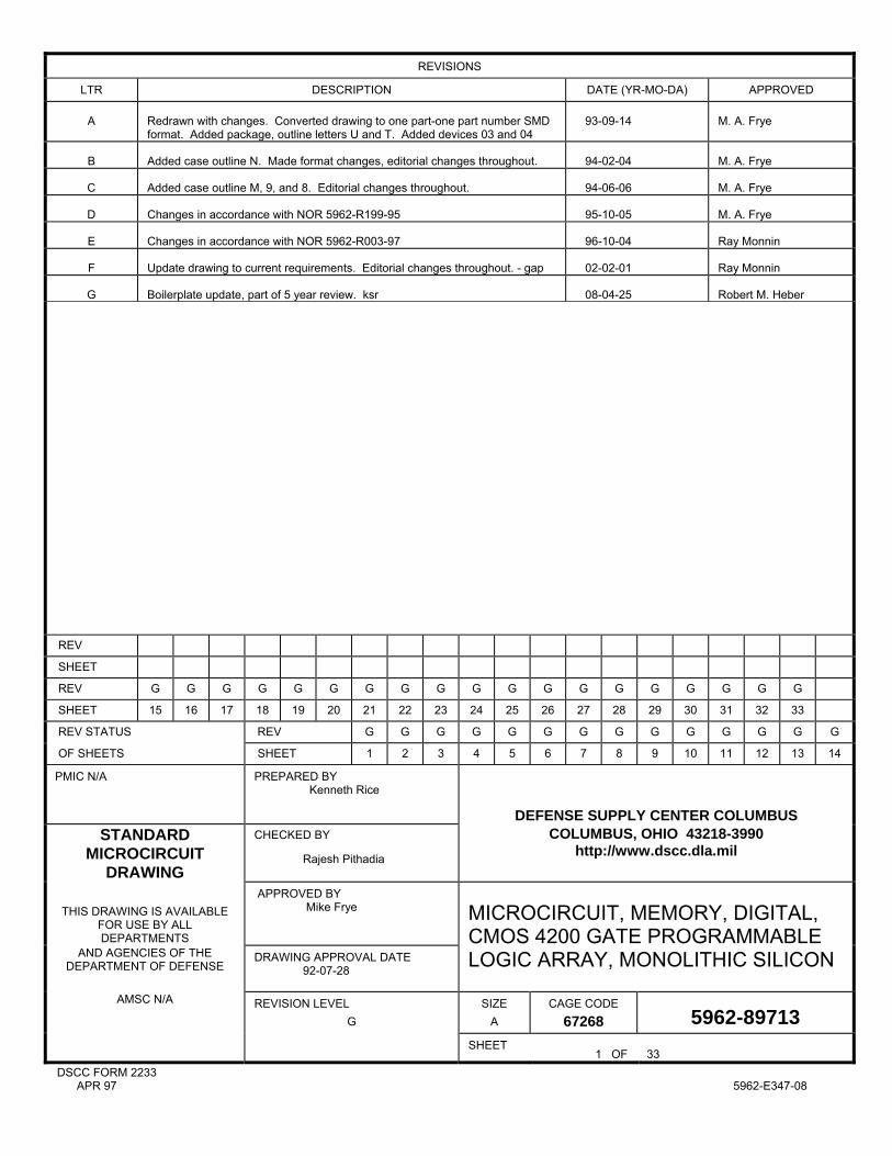
REVISIONS
LTR DESCRIPTION DATE (YR-MO-DA) APPROVED
A Redrawn with changes. Converted drawing to one part-one part number SMD format. Added package, outline letters U and T. Added devices 03 and 04
93-09-14
M. A. Frye
B
Added case outline N. Made format changes, editorial changes throughout.
94-02-04
M. A. Frye
C
Added case outline M, 9, and 8. Editorial changes throughout.
94-06-06
M. A. Frye
D
Changes in accordance with NOR 5962-R199-95
95-10-05
M. A. Frye
E
Changes in accordance with NOR 5962-R003-97
96-10-04
Ray Monnin
F
Update drawing to current requirements. Editorial changes throughout. - gap
02-02-01
Ray Monnin
G
Boilerplate update, part of 5 year review. ksr
08-04-25
Robert M. Heber
REV
SHEET
REV G G G G G G G G G G G G G G G G G G G
SHEET 15 16 17 18 19 20 21 22 23 24 25 26 27 28 29 30 31 32 33
REV STATUS REV G G G G G G G G G G G G G G
OF SHEETS SHEET 1 2 3 4 5 6 7 8 9 10 11 12 13 14
PMIC N/A PREPARED BY Kenneth Rice
DEFENSE SUPPLY CENTER COLUMBUS STANDARD
MICROCIRCUIT DRAWING
CHECKED BY Rajesh Pithadia
COLUMBUS, OHIO 43218-3990 http://www.dscc.dla.mil
THIS DRAWING IS AVAILABLE
FOR USE BY ALL DEPARTMENTS
APPROVED BY Mike Frye
AND AGENCIES OF THE DEPARTMENT OF DEFENSE
DRAWING APPROVAL DATE 92-07-28
MICROCIRCUIT, MEMORY, DIGITAL, CMOS 4200 GATE PROGRAMMABLE LOGIC ARRAY, MONOLITHIC SILICON
AMSC N/A
REVISION LEVEL G
SIZE A
CAGE CODE 67268
5962-89713
SHEET 1 OF
33
DSCC FORM 2233 APR 97 5962-E347-08

STANDARD MICROCIRCUIT DRAWING
SIZE A
5962-89713
DEFENSE SUPPLY CENTER COLUMBUS COLUMBUS, OHIO 43218-3990
REVISION LEVEL G
SHEET 2
DSCC FORM 2234 APR 97
1. SCOPE 1.1 Scope. This drawing documents two product assurance class levels consisting of high reliability (device classes Q and M) and space application (device class V). A choice of case outlines and lead finishes are available and are reflected in the Part or Identifying Number (PIN). When available, a choice of Radiation Hardness Assurance (RHA) levels are reflected in the PIN. 1.2 PIN. The PIN is as shown in the following example:
5962 - 89713 01 M X A
Federal stock class designator
RHA designator (see 1.2.1)
Device type
(see 1.2.2)
Device class
designator
Case outline
(see 1.2.4)
Lead finish
(see 1.2.5)\ / (see 1.2.3)
\/ Drawing number
1.2.1 RHA designator. Device classes Q and V RHA marked devices meet the MIL-PRF-38535 specified RHA levels and are marked with the appropriate RHA designator. Device class M RHA marked devices meet the MIL-PRF-38535, appendix A specified RHA levels and are marked with the appropriate RHA designator. A dash (-) indicates a non-RHA device. 1.2.2 Device type(s). The device type(s) identify the circuit function as follows:
Device type Generic number Circuit function Toggle Speed
01 3042-50 12x12 4200 gate programmable array 50 MHz 02 3042-70 12x12 4200 gate programmable array 70 MHz 03 3042-100 12x12 4200 gate programmable array 100 MHz 04 3042-125 12x12 4200 gate programmable array 125 MHz
1.2.3 Device class designator. The device class designator is a single letter identifying the product assurance level as follows:
Device class Device requirements documentation
M Vendor self-certification to the requirements for MIL-STD-883 compliant, non-JAN class level B microcircuits in accordance with MIL-PRF-38535, appendix A
Q or V Certification and qualification to MIL-PRF-38535
1.2.4 Case outline(s). The case outline(s) are as designated in MIL-STD-1835 and as follows:
Outline letter Descriptive designator Terminals Package style X CMGA15-PN 84 1/ Pin grid array package Y See figure 1 100 Quad flat package Z CMGA6-PN 132 2/ Pin grid array package U CMGA3-PN 84 1/ Pin grid array package T CQCC1-F100 100 Unformed-lead chip carrier 3/ N See figure 1 100 Quad flat package M See figure 1 100 Quad flat package 9 See figure 1 100 Quad flat package 8 See figure 1 100 Quad flat package 1.2.5 Lead finish. The lead finish is as specified in MIL-PRF-38535 for device classes Q and V or MIL-PRF-38535, appendix A for device class M. ________ 1/ 84 = actual number of pins used, not maximum listed in MIL-STD-1835. 2/ 132 = actual number of pins used, not maximum listed in MIL-STD-1835. 3/ Pin 1 is the middle pin on the side with center justified identifier mark. Mark may be a notch, dot, or triangle.

STANDARD MICROCIRCUIT DRAWING
SIZE A
5962-89713
DEFENSE SUPPLY CENTER COLUMBUS COLUMBUS, OHIO 43218-3990
REVISION LEVEL G
SHEET 3
DSCC FORM 2234 APR 97
1.3 Absolute maximum ratings. 3/ Supply voltage range to ground potential (VCC) ......................... -0.5 V dc to +7.0 V dc DC input voltage range .............................................................. -0.5 V dc to VCC +0.5 V dc Voltage applied to three-state output(VTS) ................................. -0.5 V dc to VCC +0.5 V dc Lead temperature (soldering, 10 seconds) ................................ +260°C Thermal resistance, junction-to-case (θJC): Case outline X, Z, U, and T ....................................................... See MIL-STD-1835 Case outlines Y, N, M, 9, and 8 ................................................. 10°C/W 4/ Junction temperature (TJ) .......................................................... +150°C 5/ Storage temperature range ....................................................... -65°C to +150°C
1.4 Recommended operating conditions. 6/
Case operating temperature range(TC) ..................................... -55°C to +125°C Supply voltage relative to ground(VCC) ...................................... +4.5 V dc minimum to +5.5 V dc maximum Ground voltage (GND) or (VSS) ................................................. 0 V dc
1.5 Digital logic testing for device classes Q and V.
Fault coverage measurement of manufacturing logic tests in accordance with MIL-PRF-38535 .......................... 95 percent
2. APPLICABLE DOCUMENTS 2.1 Government specification, standards, and handbooks. The following specification, standards, and handbooks form a part of this drawing to the extent specified herein. Unless otherwise specified, the issues of these documents are those cited in the solicitation or contract. DEPARTMENT OF DEFENSE SPECIFICATION MIL-PRF-38535 - Integrated Circuits, Manufacturing, General Specification for. DEPARTMENT OF DEFENSE STANDARDS MIL-STD-883 - Test Method Standard Microcircuits. MIL-STD-1835 - Interface Standard Electronic Component Case Outlines. DEPARTMENT OF DEFENSE HANDBOOKS MIL-HDBK-103 - List of Standard Microcircuit Drawings. MIL-HDBK-780 - Standard Microcircuit Drawings. (Copies of these documents are available online at http://assist.daps.dla.mil/quicksearch/ or http://assist.daps.dla.mil from the Standardization Document Order Desk, 700 Robins Avenue, Building 4D, Philadelphia, PA 19111-5094.) 2.2 Non-Government publications. The following document(s) form a part of this document to the extent specified herein. Unless otherwise specified, the issues of these documents are those cited in the solicitation. ELECTRONICS INDUSTRIES ASSOCIATION (EIA)
JEDEC Standard EIA/JESD78 - IC Latch-Up Test.
(Applications for copies should be addressed to the Electronics Industries Association, 2500 Wilson Boulevard, Arlington, VA 22201; http://www.jedec.org.)
(Non-Government standards and other publications are normally available from the organizations that prepare or distribute the documents. These documents also may be available in or through libraries or other informational services.) 3/ Stresses above the absolute maximum rating may cause permanent damage to the device. Extended operation at the
maximum levels may degrade performance and affect reliability. 4/ When a thermal resistance for this case is specified in MIL-STD-1835 that value shall supersede the value indicated
herein. 5/ Maximum junction temperature shall not be exceeded except for allowable short duration burn-in screening conditions in
accordance with method 5004 of MIL-STD-883. 6/ All voltage values in this drawing are with respect to VSS.

STANDARD MICROCIRCUIT DRAWING
SIZE A
5962-89713
DEFENSE SUPPLY CENTER COLUMBUS COLUMBUS, OHIO 43218-3990
REVISION LEVEL G
SHEET 4
DSCC FORM 2234 APR 97
2.3 Order of precedence. In the event of a conflict between the text of this drawing and the references cited herein, the text of this drawing takes precedence. Nothing in this document, however, supersedes applicable laws and regulations unless a specific exemption has been obtained. 3. REQUIREMENTS 3.1 Item requirements. The individual item requirements for device classes Q and V shall be in accordance with MIL-PRF-38535 and as specified herein or as modified in the device manufacturer's Quality Management (QM) plan. The modification in the QM plan shall not affect the form, fit, or function as described herein. The individual item requirements for device class M shall be in accordance with MIL-PRF-38535, appendix A for non-JAN class level B devices and as specified herein. 3.2 Design, construction, and physical dimensions. The design, construction, and physical dimensions shall be as specified in MIL-PRF-38535 and herein for device classes Q and V or MIL-PRF-38535, appendix A and herein for device class M. 3.2.1 Case outlines. The case outlines shall be in accordance with 1.2.4 herein and figure 1. 3.2.2 Terminal connections. The terminal connections shall be as specified on figure 2. 3.2.3 Logic block diagram. The logic block diagram shall be as specified on figure 3. 3.3 Electrical performance characteristics and postirradiation parameter limits. Unless otherwise specified herein, the electrical performance characteristics and postirradiation parameter limits are as specified in table I and shall apply over the full case operating temperature range. 3.4 Electrical test requirements. The electrical test requirements shall be the subgroups specified in table IIA. The electrical tests for each subgroup are defined in table I. 3.5 Marking. The part shall be marked with the PIN listed in 1.2 herein. In addition, the manufacturer's PIN may also be marked. For packages where marking of the entire SMD PIN number is not feasible due to space limitations, the manufacturer has the option of not marking the "5962-" on the device. For RHA product using this option, the RHA designator shall still be marked. Marking for device classes Q and V shall be in accordance with MIL-PRF-38535. Marking for device class M shall be in accordance with MIL-PRF-38535, appendix A. 3.5.1 Certification/compliance mark. The certification mark for device classes Q and V shall be a "QML" or "Q" as required in MIL-PRF-38535. The compliance mark for device class M shall be a "C" as required in MIL-PRF-38535, appendix A. 3.6 Certificate of compliance. For device classes Q and V, a certificate of compliance shall be required from a QML-38535 listed manufacturer in order to supply to the requirements of this drawing (see 6.7.1 herein). For device class M, a certificate of compliance shall be required from a manufacturer in order to be listed as an approved source of supply in MIL-HDBK-103 (see 6.7.2 herein). The certificate of compliance submitted to DSCC-VA prior to listing as an approved source of supply for this drawing shall affirm that the manufacturer's product meets, for device classes Q and V, the requirements of MIL-PRF-38535 and herein or for device class M, the requirements of MIL-PRF-38535, appendix A and herein. 3.7 Certificate of conformance. A certificate of conformance as required for device classes Q and V in MIL-PRF-38535 or for device class M in MIL-PRF-38535, appendix A shall be provided with each lot of microcircuits delivered to this drawing. 3.8 Notification of change for device class M. For device class M, notification to DSCC-VA of change of product (see 6.2 herein) involving devices acquired to this drawing is required for any change that affects this drawing. 3.9 Verification and review for device class M. For device class M, DSCC, DSCC's agent, and the acquiring activity retain the option to review the manufacturer's facility and applicable required documentation. Offshore documentation shall be made available onshore at the option of the reviewer. 3.10 Microcircuit group assignment for device class M. Device class M devices covered by this drawing shall be in microcircuit group number 42 (see MIL-PRF-38535, appendix A).
3.11 Operational notes. Additional information shall be provided by the device manufacturer (see 6.6 herein).
STANDARD MICROCIRCUIT DRAWING
SIZE A
5962-89713
DEFENSE SUPPLY CENTER COLUMBUS COLUMBUS, OHIO 43218-3990
REVISION LEVEL G
SHEET 5
DSCC FORM 2234 APR 97
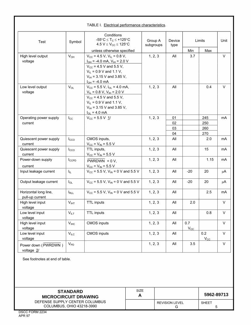
TABLE I. Electrical performance characteristics.
Test
Symbol
Conditions -55°C ≤ TC ≤ +125°C 4.5 V ≤ VCC ≤ 125°C
Group A
subgroups
Device
type
Limits
Unit
unless otherwise specified Min Max High level output VOH VCC = 4.5 V, VIL = 0.8 V, 1, 2, 3 All 3.7 V voltage IOH = -4.0 mA, VIH = 2.0 V VCC = 4.5 V and 5.5 V, VIL = 0.9 V and 1.1 V, VIH = 3.15 V and 3.85 V, IOH = -4.0 mA Low level output VOL VCC = 5.5 V, IOL = 4.0 mA, 1, 2, 3 All 0.4 V voltage VIL = 0.8 V, VIH = 2.0 V VCC = 4.5 V and 5.5 V, VIL = 0.9 V and 1.1 V, VIH = 3.15 V and 3.85 V, IOL = 4.0 mA Operating power supply ICC VCC = 5.5 V 1/ 1, 2, 3 01 245 mA current 02 250 03 260 04 270 Quiescent power supply ICCO CMOS inputs, 1, 2, 3 All 2.0 mA current VCC = VIN = 5.5 V Quiescent power supply ICCO TTL inputs, 1, 2, 3 All 15 mA current VCC = VIN = 5.5 V Power-down supply ICCPD PWRDWN = 0 V, 1, 2, 3 All 1.15 mA
current VCC = VIN = 5.5 V Input leakage current
IIL VCC = 5.5 V, VIN = 0 V and 5.5 V 1, 2, 3 All -20 20 μA
Output leakage current
IOL VCC = 5.5 V, VIN = 0 V and 5.5 V 1, 2, 3 All -20 20 μA
Horizontal long line, IRLL VCC = 5.5 V, VIN = 0 V and 5.5 V 1, 2, 3 All 2.5 mA pull-up current High level input VIHT TTL inputs 1, 2, 3 All 2.0 V voltage Low level input VILT TTL inputs 1, 2, 3 All 0.8 V voltage High level input VIHC CMOS inputs 1, 2, 3 All 0.7 V voltage VCC Low level input VILC CMOS inputs 1, 2, 3 All 0.2 V voltage VCC
Power down ( PWRDWN ) VPD 1, 2, 3 All 3.5 V
voltage 2/ See footnotes at end of table.
STANDARD MICROCIRCUIT DRAWING
SIZE A
5962-89713
DEFENSE SUPPLY CENTER COLUMBUS COLUMBUS, OHIO 43218-3990
REVISION LEVEL G
SHEET 6
DSCC FORM 2234 APR 97
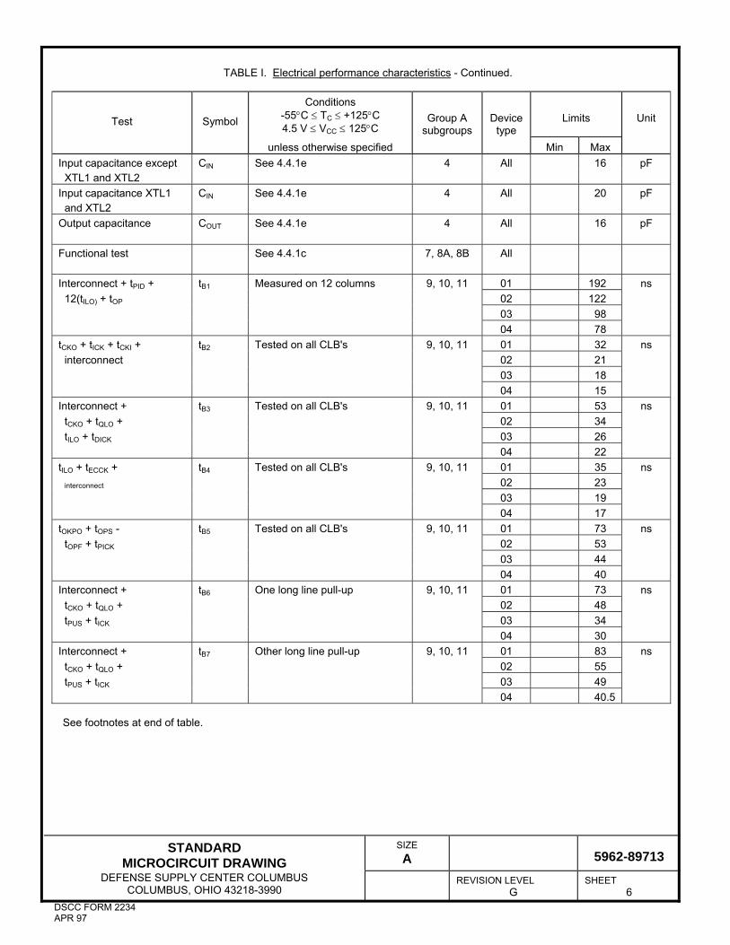
TABLE I. Electrical performance characteristics - Continued.
Test
Symbol
Conditions -55°C ≤ TC ≤ +125°C 4.5 V ≤ VCC ≤ 125°C
Group A
subgroups
Device
type
Limits
Unit
unless otherwise specified Min Max Input capacitance except CIN See 4.4.1e 4 All 16 pF XTL1 and XTL2 Input capacitance XTL1 CIN See 4.4.1e 4 All 20 pF and XTL2 Output capacitance
COUT See 4.4.1e 4 All 16 pF
Functional test
See 4.4.1c 7, 8A, 8B All
Interconnect + tPID + tB1 Measured on 12 columns 9, 10, 11 01 192 ns 12(tILO) + tOP 02 122 03 98 04 78 tCKO + tICK + tCKI + tB2 Tested on all CLB's 9, 10, 11 01 32 ns interconnect 02 21 03 18 04 15 Interconnect + tB3 Tested on all CLB's 9, 10, 11 01 53 ns tCKO + tQLO + 02 34 tILO + tDICK 03 26 04 22 tILO + tECCK + tB4 Tested on all CLB's 9, 10, 11 01 35 ns interconnect 02 23 03 19 04 17 tOKPO + tOPS - tB5 Tested on all CLB's 9, 10, 11 01 73 ns tOPF + tPICK 02 53 03 44 04 40 Interconnect + tB6 One long line pull-up 9, 10, 11 01 73 ns tCKO + tQLO + 02 48 tPUS + tICK 03 34 04 30 Interconnect + tB7 Other long line pull-up 9, 10, 11 01 83 ns tCKO + tQLO + 02 55 tPUS + tICK 03 49 04 40.5 See footnotes at end of table.

STANDARD MICROCIRCUIT DRAWING
SIZE A
5962-89713
DEFENSE SUPPLY CENTER COLUMBUS COLUMBUS, OHIO 43218-3990
REVISION LEVEL G
SHEET 7
DSCC FORM 2234 APR 97
TABLE I. Electrical performance characteristics - Continued.
Test
Symbol
Conditions -55°C ≤ TC ≤ +125°C 4.5 V ≤ VCC ≤ 125°C
Group A
subgroups
Device
type
Limits
Unit
unless otherwise specified Min Max Interconnect + tB8 No pull-up, lower long 9, 10, 11 01 47 ns tCKO + tQLO + lines 02 31 tIO + tICK 03 25 04 22 Interconnect + tB9 No pull-up, upper long 9, 10, 11 01 57 ns tCKO + tQLO + lines 02 38 tICK + tIO 03 32 04 28 Logic input to output tILO See figure 4 3/ 01 14 ns (combinatorial) 02 9 03 7 04 5.5 Reset input to output tRIO 3/ 01 15 ns 02 8 03 7 04 6 Reset direct width tRPW 3/ 01 12 ns 02 8 03 7 04 6 Master reset pin to CLB tMRQ 3/ 01 30 ns output (X and Y) 02 24 03 19 04 17 K clock input to CLB tCKO 3/ 01 12 ns output 02 8 03 6 04 5 Clock K to the outputs tQLO 3/ 01 25 ns X or Y when Q is return 02 13 through the function 03 10 generators to drive X 04 8 or Y K clock logic-input tICK 3/ 01 12 ns setup 02 8 03 7 04 5 K clock logic-input hold
tCKI 3/ All 1 ns
See footnotes at end of table.
STANDARD MICROCIRCUIT DRAWING
SIZE A
5962-89713
DEFENSE SUPPLY CENTER COLUMBUS COLUMBUS, OHIO 43218-3990
REVISION LEVEL G
SHEET 8
DSCC FORM 2234 APR 97
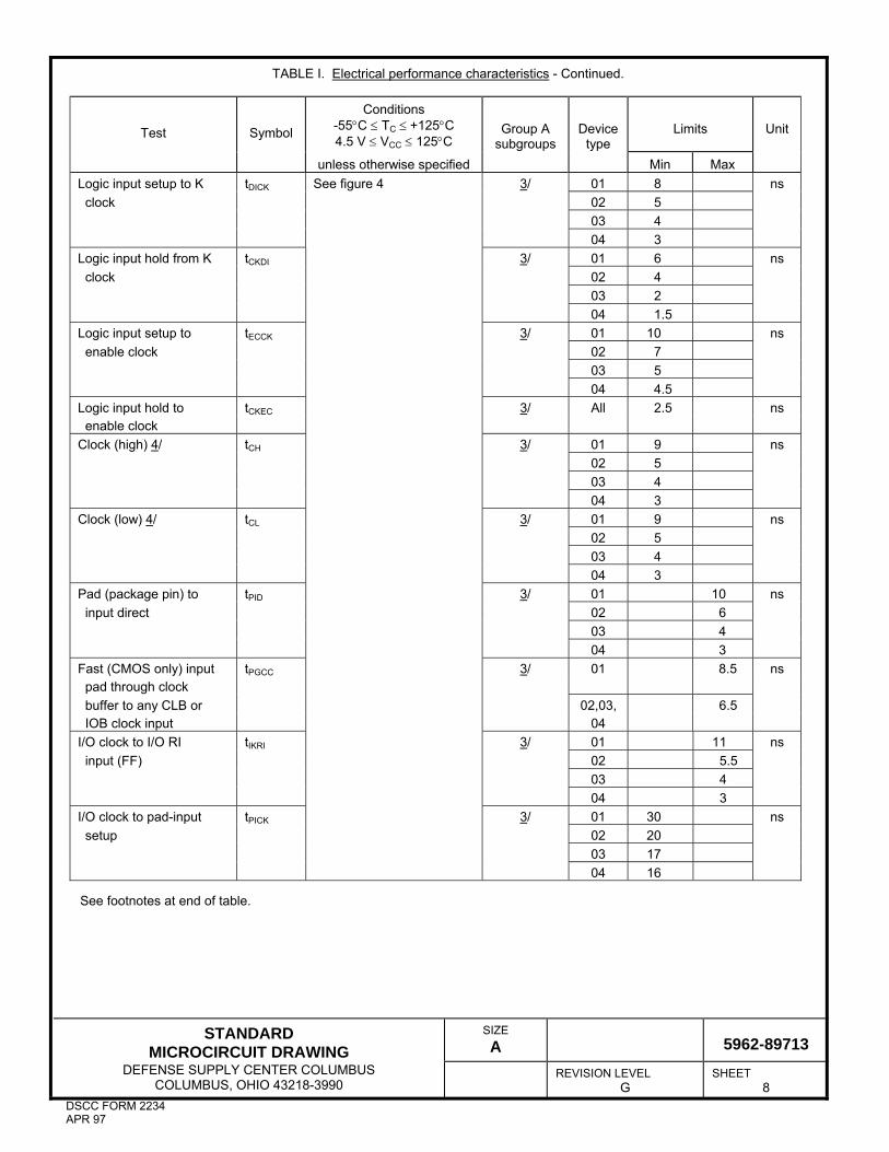
TABLE I. Electrical performance characteristics - Continued.
Test
Symbol
Conditions -55°C ≤ TC ≤ +125°C 4.5 V ≤ VCC ≤ 125°C
Group A
subgroups
Device
type
Limits
Unit
unless otherwise specified Min Max Logic input setup to K tDICK See figure 4 3/ 01 8 ns clock 02 5 03 4 04 3 Logic input hold from K tCKDI 3/ 01 6 ns clock 02 4 03 2 04 1.5 Logic input setup to tECCK 3/ 01 10 ns enable clock 02 7 03 5 04 4.5 Logic input hold to tCKEC 3/ All 2.5 ns enable clock Clock (high) 4/ tCH 3/ 01 9 ns 02 5 03 4 04 3 Clock (low) 4/ tCL 3/ 01 9 ns 02 5 03 4 04 3 Pad (package pin) to tPID 3/ 01 10 ns input direct 02 6 03 4 04 3 Fast (CMOS only) input tPGCC 3/ 01 8.5 ns pad through clock buffer to any CLB or 02,03, 6.5 IOB clock input 04 I/O clock to I/O RI tIKRI 3/ 01 11 ns input (FF) 02 5.5 03 4 04 3 I/O clock to pad-input tPICK 3/ 01 30 ns setup 02 20 03 17 04 16 See footnotes at end of table.

STANDARD MICROCIRCUIT DRAWING
SIZE A
5962-89713
DEFENSE SUPPLY CENTER COLUMBUS COLUMBUS, OHIO 43218-3990
REVISION LEVEL G
SHEET 9
DSCC FORM 2234 APR 97
TABLE I. Electrical performance characteristics - Continued.
Test
Symbol
Conditions -55°C ≤ TC ≤ +125°C 4.5 V ≤ VCC ≤ 125°C
Group A
subgroups
Device
type
Limits
Unit
unless otherwise specified Min Max I/0 clock to pad-input tIKPI See figure 4 3/ All 0 ns hold I/O clock to pad (fast) tOKPO 3/ 01 18 ns 02 13 03 10 04 9 I/O clock to pad-output tOOK 3/ 01 15 ns setup 02 10 03 9 04 8 I/O clock to pad-output tOKO 3/ All 0 ns hold I/O clock (high) 5/ tIOH 3/ 01 9 ns 02 5 03 4 04 3 I/O clock (low) 5/ tIOL 3/ 01 9 ns 02 5 03 4 04 3 Output (enabled fast) tOPF 3/ 01 15 ns to pad 02 9 03 6 04 5 Output (enabled slow) tOPS 3/ 01 40 ns to pad 02 33 03 24 04 20 Three-state to pad begin tTSHZ 3/ 01 14 ns high impedance (fast) 02 12 03 10 04 9 Three-state to pad end tTSON 3/ 01 20 ns high impedance (fast) 02 14 03 12 04 11 Master RESET to input tRRI 3/ 01 37 ns RI 02 27 03, 04 24 See footnotes at end of table.
STANDARD MICROCIRCUIT DRAWING
SIZE A
5962-89713
DEFENSE SUPPLY CENTER COLUMBUS COLUMBUS, OHIO 43218-3990
REVISION LEVEL G
SHEET 10
DSCC FORM 2234 APR 97
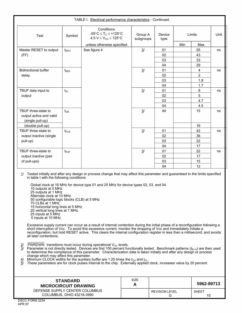
TABLE I. Electrical performance characteristics - Continued.
Test
Symbol
Conditions -55°C ≤ TC ≤ +125°C 4.5 V ≤ VCC ≤ 125°C
Group A
subgroups
Device
type
Limits
Unit
unless otherwise specified Min Max Master RESET to output tRPO See figure 4 3/ 01 55 ns (FF) 02 43 03 33 04 29 Bidirectional buffer tBIDI 3/ 01 4 ns delay 02 2 03 1.8 04 1.7 TBUF data input to tIO 3/ 01 8 ns output 02 5 03 4.7 04 4.5 TBUF three-state to tON 3/ All 15 ns output active and valid (single pull-up) (double pull-up) 16 TBUF three-state to tPUS 3/ 01 42 ns output inactive (single 02 36 pull-up) 03 22 04 17 TBUF three-state to tPUF 3/ 01 22 ns output inactive (pair 02 17 of pull-ups) 03 15 04 12 1/ Tested initially and after any design or process change that may affect this parameter and guaranteed to the limits specified
in table I with the following conditions:
Global clock at 16 MHz for device type 01 and 25 MHz for device types 02, 03, and 04. 10 outputs at 5 MHz 25 outputs at 1 MHz Alternate clock at 10 MHz 50 configurable logic blocks (CLB) at 5 MHz 75 CLBs at 1 MHz 15 horizontal long lines at 5 MHz 20 vertical long lines at 1 MHz 25 inputs at 5 MHz
5 inputs at 10 MHz
Excessive supply current can occur as a result of internal contention during the initial phase of a reconfiguration following a short interruption of Vcc. To avoid this excessive current, monitor the dropping of Vcc and immediately initiate a reconfiguration, but hold RESET active. This clears the internal configuration register in less than a millisecond, and avoids all later contentions.
2/ PWRDWN transitions must occur during operational VCC levels. 3/ Parameter is not directly tested. Devices are first 100 percent functionally tested. Benchmark patterns (tB1-9) are then used
to determine the compliance of this parameter. Characterization data is taken initially and after any design or process change which may affect this parameter.
4/ Minimum CLOCK widths for the auxiliary buffer are 1.25 times the tCH and tCL. 5/ These parameters are for clock pulses internal to the chip. Externally applied clock, increases value by 20 percent.
STANDARD MICROCIRCUIT DRAWING
SIZE A
5962-89713
DEFENSE SUPPLY CENTER COLUMBUS COLUMBUS, OHIO 43218-3990
REVISION LEVEL G
SHEET 11
DSCC FORM 2234 APR 97
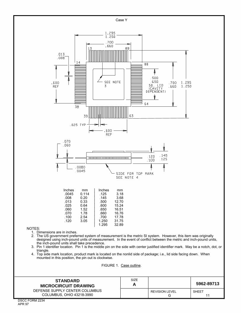
Case Y
Inches mm │ Inches mm .0045 0.114 │ .125 3.18 .008 0.20 │ .145 3.68 .013 0.33 │ .500 12.70 .025 0.64 │ .600 15.24 .060 1.52 │ .650 16.51 .070 1.78 │ .660 16.76 .100 2.54 │ .700 17.78 .120 3.05 │ 1.250 31.75 │ 1.295 32.89 NOTES:
1. Dimensions are in inches. 2. The US government preferred system of measurement is the metric SI system. However, this item was originally
designed using inch-pound units of measurement. In the event of conflict between the metric and inch-pound units, the inch-pound units shall take precedence.
3. Pin 1 identifier location. Pin 1 is the middle pin on the side with center justified identifier mark. May be a notch, dot, or triangle.
4. Top side mark location, product mark is located on the nonlid side of package; i.e., lid side facing down. When mounted in this position, the pin out is clockwise.
FIGURE 1. Case outline.
STANDARD MICROCIRCUIT DRAWING
SIZE A
5962-89713
DEFENSE SUPPLY CENTER COLUMBUS COLUMBUS, OHIO 43218-3990
REVISION LEVEL G
SHEET 12
DSCC FORM 2234 APR 97
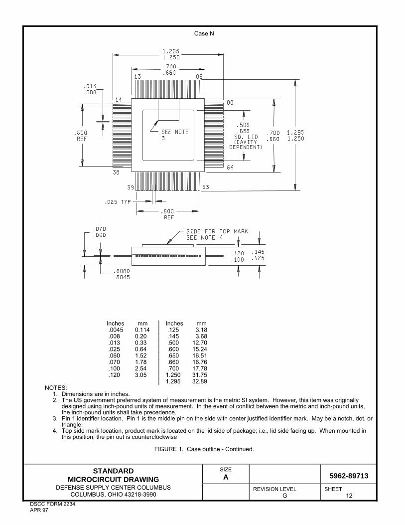
Case N
Inches mm │ Inches mm .0045 0.114 │ .125 3.18 .008 0.20 │ .145 3.68 .013 0.33 │ .500 12.70 .025 0.64 │ .600 15.24 .060 1.52 │ .650 16.51 .070 1.78 │ .660 16.76 .100 2.54 │ .700 17.78 .120 3.05 │ 1.250 31.75 │ 1.295 32.89 NOTES:
1. Dimensions are in inches. 2. The US government preferred system of measurement is the metric SI system. However, this item was originally
designed using inch-pound units of measurement. In the event of conflict between the metric and inch-pound units, the inch-pound units shall take precedence.
3. Pin 1 identifier location. Pin 1 is the middle pin on the side with center justified identifier mark. May be a notch, dot, or triangle.
4. Top side mark location, product mark is located on the lid side of package; i.e., lid side facing up. When mounted in this position, the pin out is counterclockwise
FIGURE 1. Case outline - Continued.
STANDARD MICROCIRCUIT DRAWING
SIZE A
5962-89713
DEFENSE SUPPLY CENTER COLUMBUS COLUMBUS, OHIO 43218-3990
REVISION LEVEL G
SHEET 13
DSCC FORM 2234 APR 97
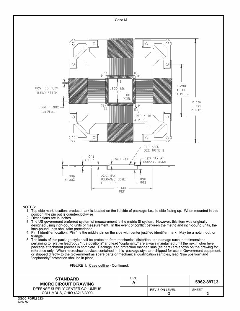
Case M NOTES:
1. Top side mark location, product mark is located on the lid side of package; i.e., lid side facing up. When mounted in this position, the pin out is counterclockwise
2. Dimensions are in inches. 3. The US government preferred system of measurement is the metric SI system. However, this item was originally
designed using inch-pound units of measurement. In the event of conflict between the metric and inch-pound units, the inch-pound units shall take precedence.
4. Pin 1 identifier location. Pin 1 is the middle pin on the side with center justified identifier mark. May be a notch, dot, or triangle.
5. The leads of this package style shall be protected from mechanical distortion and damage such that dimensions pertaining to relative lead/body "true positions" and lead "coplanarity" are always maintained until the next higher level package attachment process is complete. Package lead protection mechanisms (tie bars) are shown on the drawing for reference only. When microcircuit devices contained in this package style are shipped for use in Government equipment, or shipped directly to the Government as spare parts or mechanical qualification samples, lead "true position" and "coplanarity" protection shall be in place.
FIGURE 1. Case outline - Continued.
STANDARD MICROCIRCUIT DRAWING
SIZE A
5962-89713
DEFENSE SUPPLY CENTER COLUMBUS COLUMBUS, OHIO 43218-3990
REVISION LEVEL G
SHEET 14
DSCC FORM 2234 APR 97
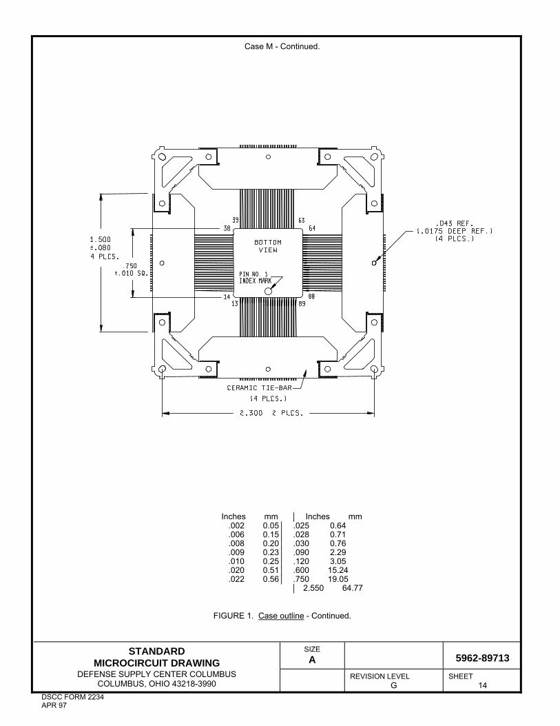
Case M - Continued.
Inches mm │ Inches mm .002 0.05 │ .025 0.64 .006 0.15 │ .028 0.71 .008 0.20 │ .030 0.76 .009 0.23 │ .090 2.29 .010 0.25 │ .120 3.05 .020 0.51 │ .600 15.24 .022 0.56 │ .750 19.05 │ 2.550 64.77 FIGURE 1. Case outline - Continued.
STANDARD MICROCIRCUIT DRAWING
SIZE A
5962-89713
DEFENSE SUPPLY CENTER COLUMBUS COLUMBUS, OHIO 43218-3990
REVISION LEVEL G
SHEET 15
DSCC FORM 2234 APR 97
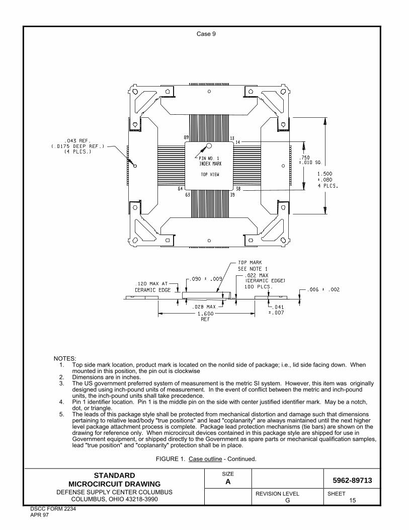
Case 9
NOTES: 1. Top side mark location, product mark is located on the nonlid side of package; i.e., lid side facing down. When
mounted in this position, the pin out is clockwise 2. Dimensions are in inches. 3. The US government preferred system of measurement is the metric SI system. However, this item was originally
designed using inch-pound units of measurement. In the event of conflict between the metric and inch-pound units, the inch-pound units shall take precedence.
4. Pin 1 identifier location. Pin 1 is the middle pin on the side with center justified identifier mark. May be a notch, dot, or triangle.
5. The leads of this package style shall be protected from mechanical distortion and damage such that dimensions pertaining to relative lead/body "true positions" and lead "coplanarity" are always maintained until the next higher level package attachment process is complete. Package lead protection mechanisms (tie bars) are shown on the drawing for reference only. When microcircuit devices contained in this package style are shipped for use in Government equipment, or shipped directly to the Government as spare parts or mechanical qualification samples, lead "true position" and "coplanarity" protection shall be in place.
FIGURE 1. Case outline - Continued.

STANDARD MICROCIRCUIT DRAWING
SIZE A
5962-89713
DEFENSE SUPPLY CENTER COLUMBUS COLUMBUS, OHIO 43218-3990
REVISION LEVEL G
SHEET 16
DSCC FORM 2234 APR 97
Case 9 - Continued.
Inches mm │ Inches mm .002 0.05 │ .025 0.64 .006 0.15 │ .028 0.71 .008 0.20 │ .030 0.76 .009 0.23 │ .090 2.29 .010 0.25 │ .120 3.05 .020 0.51 │ .600 15.24 .022 0.56 │ .750 19.05 │ 2.550 64.77
FIGURE 1. Case outline - Continued.
STANDARD MICROCIRCUIT DRAWING
SIZE A
5962-89713
DEFENSE SUPPLY CENTER COLUMBUS COLUMBUS, OHIO 43218-3990
REVISION LEVEL G
SHEET 17
DSCC FORM 2234 APR 97
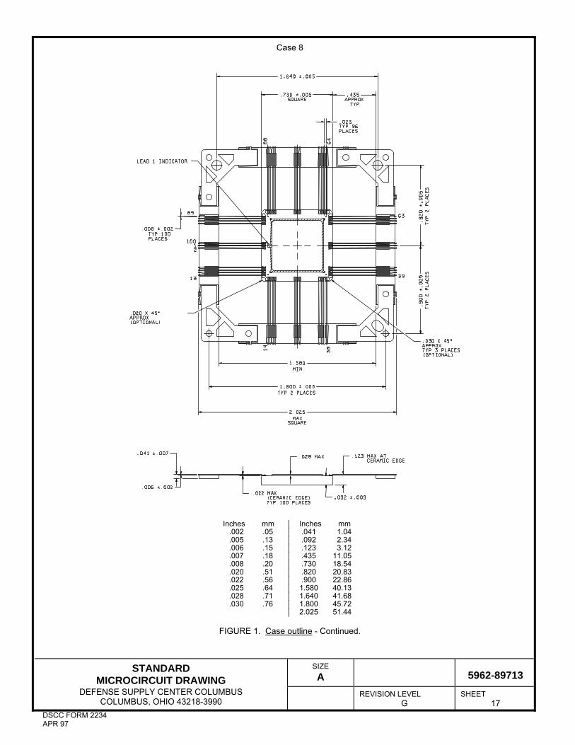
Case 8
Inches mm │ Inches mm .002 .05 │ .041 1.04 .005 .13 │ .092 2.34 .006 .15 │ .123 3.12 .007 .18 │ .435 11.05 .008 .20 │ .730 18.54 .020 .51 │ .820 20.83 .022 .56 │ .900 22.86 .025 .64 │ 1.580 40.13 .028 .71 │ 1.640 41.68 .030 .76 │ 1.800 45.72 │ 2.025 51.44
FIGURE 1. Case outline - Continued.
STANDARD MICROCIRCUIT DRAWING
SIZE A
5962-89713
DEFENSE SUPPLY CENTER COLUMBUS COLUMBUS, OHIO 43218-3990
REVISION LEVEL G
SHEET 18
DSCC FORM 2234 APR 97
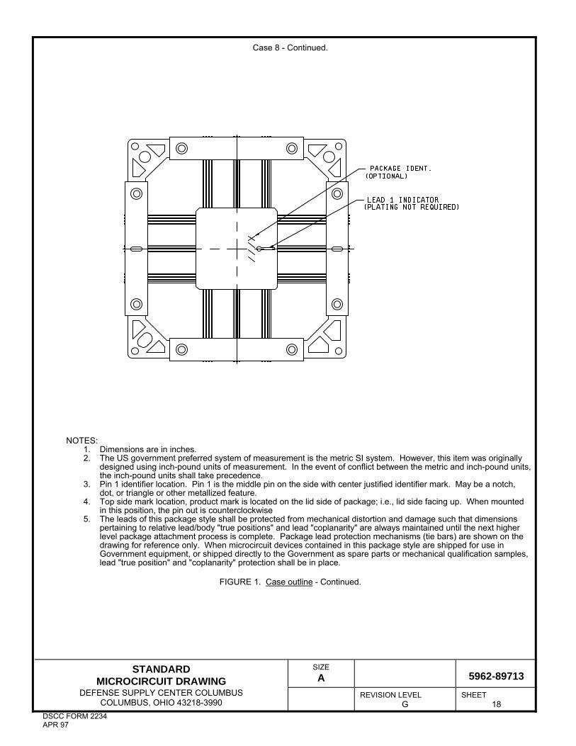
Case 8 - Continued.
NOTES:
1. Dimensions are in inches. 2. The US government preferred system of measurement is the metric SI system. However, this item was originally
designed using inch-pound units of measurement. In the event of conflict between the metric and inch-pound units, the inch-pound units shall take precedence.
3. Pin 1 identifier location. Pin 1 is the middle pin on the side with center justified identifier mark. May be a notch, dot, or triangle or other metallized feature.
4. Top side mark location, product mark is located on the lid side of package; i.e., lid side facing up. When mounted in this position, the pin out is counterclockwise
5. The leads of this package style shall be protected from mechanical distortion and damage such that dimensions pertaining to relative lead/body "true positions" and lead "coplanarity" are always maintained until the next higher level package attachment process is complete. Package lead protection mechanisms (tie bars) are shown on the drawing for reference only. When microcircuit devices contained in this package style are shipped for use in Government equipment, or shipped directly to the Government as spare parts or mechanical qualification samples, lead "true position" and "coplanarity" protection shall be in place.
FIGURE 1. Case outline - Continued.
STANDARD MICROCIRCUIT DRAWING
SIZE A
5962-89713
DEFENSE SUPPLY CENTER COLUMBUS COLUMBUS, OHIO 43218-3990
REVISION LEVEL G
SHEET 19
DSCC FORM 2234 APR 97
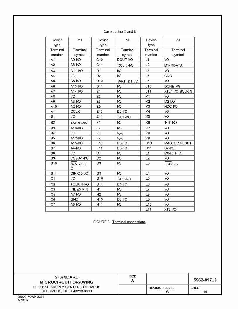
Case outline X and U
Device All Device All Device All type type type
Terminal Terminal Terminal Terminal Terminal Terminal number symbol number symbol number symbol
A1 A9-I/O C10 DOUT-I/O J1 I/O A2 A8-I/O C11 RCLK -I/O J2 M1- RDATA A3 A11-I/O D1 I/O J5 I/O A4 I/O D2 I/O J6 GND A5 A6-I/O D10 WRT -D1-I/O J7 I/O A6 A13-I/O D11 I/O J10 DONE-PG A7 A14-I/O E1 I/O J11 XTL1-I/O-BCLKIN A8 I/O E2 I/O K1 I/O A9 A3-I/O E3 I/O K2 M2-I/O A10 A2-I/O E9 I/O K3 HDC-I/O A11 CCLK E10 D2-I/O K4 I/O B1 I/O E11 CS1-I/O K5 I/O
B2 PWRDWN F1 I/O K6 INIT-I/O B3 A10-I/O F2 I/O K7 I/O B4 I/O F3 VCC K8 I/O B5 A12-I/O F9 VCC K9 I/O B6 A15-I/O F10 D5-I/O K10 MASTER RESET B7 A4-I/O F11 D3-I/O K11 D7-I/O B8 I/O G1 I/O L1 M0-RTRIG B9 CS2-A1-I/O G2 I/O L2 I/O B10 WS -A0-I/
O G3 I/O L3 LDC -I/O
B11 DIN-D0-I/O G9 I/O L4 I/O C1 I/O G10 CS0 -I/O L5 I/O
C2 TCLKIN-I/O G11 D4-I/O L6 I/O C3 INDEX PIN H1 I/O L7 I/O C5 A7-I/O H2 I/O L8 I/O C6 GND H10 D6-I/O L9 I/O C7 A5-I/O H11 I/O L10 I/O L11 XT2-I/O
FIGURE 2. Terminal connections.
STANDARD MICROCIRCUIT DRAWING
SIZE A
5962-89713
DEFENSE SUPPLY CENTER COLUMBUS COLUMBUS, OHIO 43218-3990
REVISION LEVEL G
SHEET 20
DSCC FORM 2234 APR 97
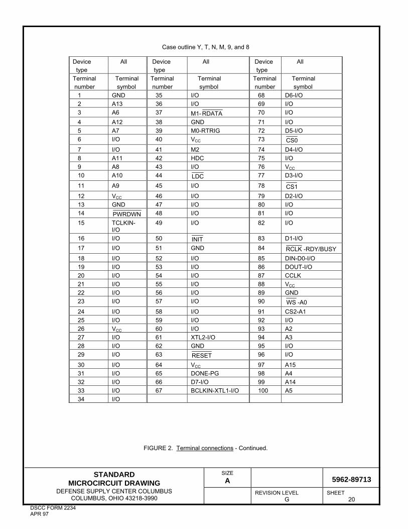
Case outline Y, T, N, M, 9, and 8
Device All Device All Device All type type type Terminal Terminal Terminal Terminal Terminal Terminal number symbol number symbol number symbol 1 GND 35 I/O 68 D6-I/O 2 A13 36 I/O 69 I/O 3 A6 37 M1- RDATA 70 I/O 4 A12 38 GND 71 I/O 5 A7 39 M0-RTRIG 72 D5-I/O 6 I/O 40 VCC 73 CS0 7 I/O 41 M2 74 D4-I/O 8 A11 42 HDC 75 I/O 9 A8 43 I/O 76 VCC 10 A10 44 LDC 77 D3-I/O
11 A9 45 I/O 78 CS1 12 VCC 46 I/O 79 D2-I/O 13 GND 47 I/O 80 I/O 14 PWRDWN 48 I/O 81 I/O 15 TCLKIN-
I/O 49 I/O 82 I/O
16 I/O 50 INIT 83 D1-I/O 17 I/O 51 GND 84 RCLK -RDY/BUSY 18 I/O 52 I/O 85 DIN-D0-I/O 19 I/O 53 I/O 86 DOUT-I/O 20 I/O 54 I/O 87 CCLK 21 I/O 55 I/O 88 VCC 22 I/O 56 I/O 89 GND 23 I/O 57 I/O 90 WS -A0 24 I/O 58 I/O 91 CS2-A1 25 I/O 59 I/O 92 I/O 26 VCC 60 I/O 93 A2 27 I/O 61 XTL2-I/O 94 A3 28 I/O 62 GND 95 I/O 29 I/O 63 RESET 96 I/O
30 I/O 64 VCC 97 A15 31 I/O 65 DONE-PG 98 A4 32 I/O 66 D7-I/O 99 A14 33 I/O 67 BCLKIN-XTL1-I/O 100 A5 34 I/O
FIGURE 2. Terminal connections - Continued.

STANDARD MICROCIRCUIT DRAWING
SIZE A
5962-89713
DEFENSE SUPPLY CENTER COLUMBUS COLUMBUS, OHIO 43218-3990
REVISION LEVEL G
SHEET 21
DSCC FORM 2234 APR 97
Case outline Z
Device All Device All Device All type type type Terminal Terminal Terminal Terminal Terminal Terminal number symbol number symbol number symbol A1 PWRDN D3 VCC L13 I/O A2 N/C D12 VCC L14 NC A3 N/C D13 I/O M1 I/O A4 I/O D14 LDC -I/O M2 A0- W5 -I/O A5 I/O E1 A7-I/O M3 DOUT-I/O A6 I/O E2 I/O M4 VCC A7 I/O E3 I/O M5 D1-I/O A8 I/O E12 I/O M6 D2-I/O A9 I/O E13 NC M7 GND A10 I/O E14 I/O M8 VCC A11 N/C F1 NC M9 D5-I/O A12 N/C F2 A12-I/O M10 I/O A13 N/C F3 I/O M11 VCC A14 MO-RT F12 I/O M12 D7-I/O B1 A10-I/O F13 I/O M13 XTAL2-I/O B2 I/O F14 I/O M14 I/O B3 I/O G1 A6-I/O N1 A1-CS2-I/O B4 I/O G2 A13-I/O N2 D0-DIN-I/O B5 I/O G3 VCC N3 I/O B6 I/O G12 VCC N4 BUSY-RCLK / B7 I/O G13 I/O RDY-I/O B8 I/O G14 INIT -I/O N5 I/O B9 I/O H1 A14-I/O N6 NC B10 I/O H2 A5-I/O N7 D3-I/O B11 I/O H3 GND N8 D4-I/O B12 I/O H12 GND N9 CS0 -I/O B13 M1- RD H13 I/O N10 I/O B14 HDC-I/O H14 I/O N11 D6-I/O C1 I/O J1 NC N12 I/O C2 A9-I/O J2 A4-I/O N13 DONE-PG C3 I/O J3 I/O N14 I/O C4 GND J12 I/O P1 CCLK C5 I/O J13 I/O P2 I/O C6 I/O J14 I/O P3 I/O C7 GND K1 A15-I/O P4 I/O C8 VCC K2 I/O P5 NC C9 I/O K3 I/O P6 CS1-I/O C10 I/O K12 I/O P7 I/O C11 GND K13 I/O P8 NC C12 I/O K14 I/O P9 NC C13 M2-I/O L1 A3-I/O P10 I/O C14 I/O L2 A2-I/O P11 NC D1 A11-I/O L3 GND P12 I/O D2 A8-I/O L12 GND P13 XTAL1-I/O P14 RESET
FIGURE 2. Terminal connections - Continued.
STANDARD MICROCIRCUIT DRAWING
SIZE A
5962-89713
DEFENSE SUPPLY CENTER COLUMBUS COLUMBUS, OHIO 43218-3990
REVISION LEVEL G
SHEET 22
DSCC FORM 2234 APR 97
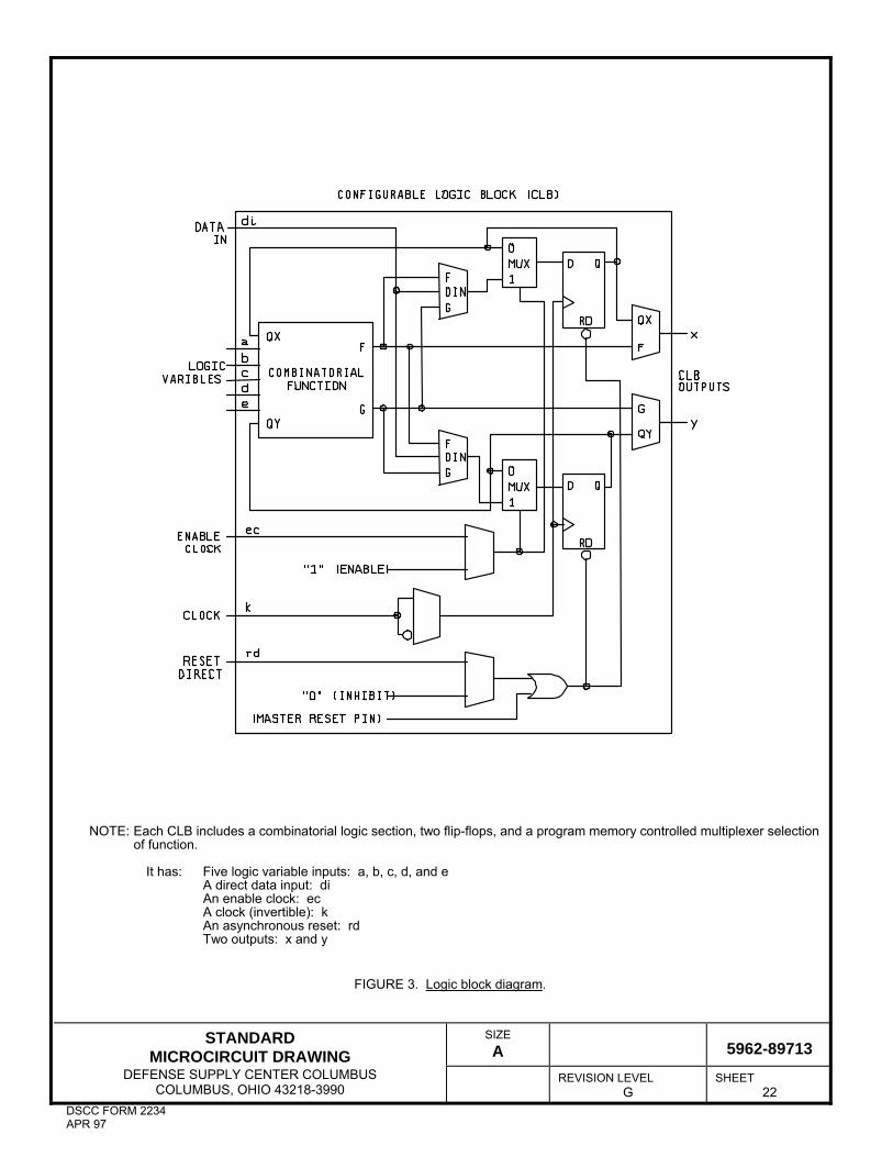
NOTE: Each CLB includes a combinatorial logic section, two flip-flops, and a program memory controlled multiplexer selection of function.
It has: Five logic variable inputs: a, b, c, d, and e
A direct data input: di An enable clock: ec A clock (invertible): k An asynchronous reset: rd Two outputs: x and y
FIGURE 3. Logic block diagram.

STANDARD MICROCIRCUIT DRAWING
SIZE A
5962-89713
DEFENSE SUPPLY CENTER COLUMBUS COLUMBUS, OHIO 43218-3990
REVISION LEVEL G
SHEET 23
DSCC FORM 2234 APR 97
NOTE: The IOB includes input and output storage elements and I/O options selected by configuration memory cells. A choice of two clocks is available on each die edge. The polarity of each clock line (not each flip-flop or latch) is programmable. A clock line that triggers the flip-flop on the rising edge is an active low latch enable (latch transparent) signal and vice versa. Passive pull-up can only be enabled on inputs, not on outputs. All user inputs are programmed for TTL or CMOS thresholds.
FIGURE 3. Logic block diagram- Continued.
STANDARD MICROCIRCUIT DRAWING
SIZE A
5962-89713
DEFENSE SUPPLY CENTER COLUMBUS COLUMBUS, OHIO 43218-3990
REVISION LEVEL G
SHEET 24
DSCC FORM 2234 APR 97
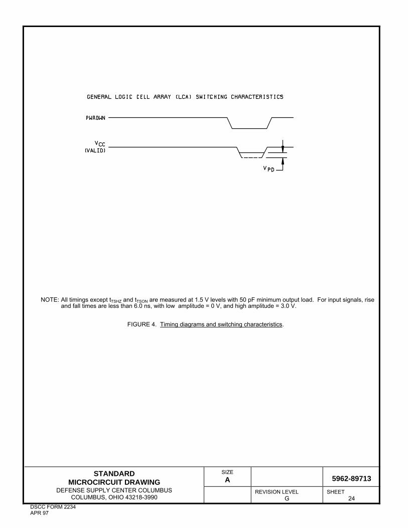
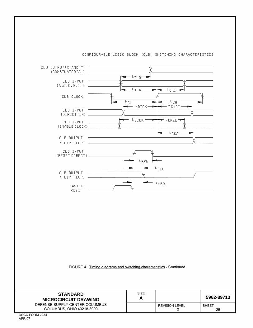
NOTE: All timings except tTSHZ and tTSON are measured at 1.5 V levels with 50 pF minimum output load. For input signals, rise and fall times are less than 6.0 ns, with low amplitude = 0 V, and high amplitude = 3.0 V.
FIGURE 4. Timing diagrams and switching characteristics.
STANDARD MICROCIRCUIT DRAWING
SIZE A
5962-89713
DEFENSE SUPPLY CENTER COLUMBUS COLUMBUS, OHIO 43218-3990
REVISION LEVEL G
SHEET 25
DSCC FORM 2234 APR 97
FIGURE 4. Timing diagrams and switching characteristics - Continued.

STANDARD MICROCIRCUIT DRAWING
SIZE A
5962-89713
DEFENSE SUPPLY CENTER COLUMBUS COLUMBUS, OHIO 43218-3990
REVISION LEVEL G
SHEET 26
DSCC FORM 2234 APR 97
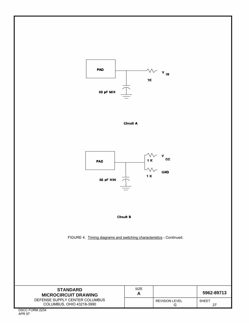
NOTE: tTSHZ is determined when the output shifts 10 percent (of the output voltage swing) from VOL level or VOH level. See
figure 5, circuit A herein for circuit used. tTSON is measured at 0.5 VCC level with VIN = 0.0 V for three-state to active High, and VIN = VCC for three-state to active low. See figure 5, circuit B herein for circuit used.
FIGURE 4. Timing diagrams and switching characteristics - Continued.
STANDARD MICROCIRCUIT DRAWING
SIZE A
5962-89713
DEFENSE SUPPLY CENTER COLUMBUS COLUMBUS, OHIO 43218-3990
REVISION LEVEL G
SHEET 27
DSCC FORM 2234 APR 97
FIGURE 4. Timing diagrams and switching characteristics - Continued.

STANDARD MICROCIRCUIT DRAWING
SIZE A
5962-89713
DEFENSE SUPPLY CENTER COLUMBUS COLUMBUS, OHIO 43218-3990
REVISION LEVEL G
SHEET 28
DSCC FORM 2234 APR 97
4. VERIFICATION 4.1 Sampling and inspection. For device classes Q and V, sampling and inspection procedures shall be in accordance with MIL-PRF-38535 or as modified in the device manufacturer's Quality Management (QM) plan. The modification in the QM plan shall not affect the form, fit, or function as described herein. For device class M, sampling and inspection procedures shall be in accordance with MIL-PRF-38535, appendix A. 4.2 Screening. For device classes Q and V, screening shall be in accordance with MIL-PRF-38535, and shall be conducted on all devices prior to qualification and technology conformance inspection. For device class M, screening shall be in accordance with method 5004 of MIL-STD-883, and shall be conducted on all devices prior to quality conformance inspection. 4.2.1 Additional criteria for device class M.
a. Delete the sequence specified as initial (pre-burn-in) electrical parameters through interim (post-burn-in) electrical parameters of method 5004 and substitute lines 1 through 6 of table IIA herein.
b. Burn-in test, method 1015 of MIL-STD-883.
(1) The test circuit shall be maintained by the manufacturer under document revision level control and shall be made
available to the preparing or acquiring activity upon request. The test circuit shall specify the inputs, outputs, biases, and power dissipation, as applicable, in accordance with the intent specified in method 1015.
(2) TA = +125°C, minimum.
c. Interim and final electrical test parameters shall be as specified in table IIA herein.
4.2.2 Additional criteria for device classes Q and V.
a. The burn-in test duration, test condition and test temperature, or approved alternatives shall be as specified in the device manufacturer's QM plan in accordance with MIL-PRF-38535. The burn-in test circuit shall be maintained under document revision level control of the device manufacturer's Technology Review Board (TRB) in accordance with
MIL-PRF-38535 and shall be made available to the acquiring or preparing activity upon request. The test circuit shall specify the inputs, outputs, biases, and power dissipation, as applicable, in accordance with the intent specified in method 1015 of MIL-STD-883.
b. Interim and final electrical test parameters shall be as specified in table IIA herein.
c. Additional screening for device class V beyond the requirements of device class Q shall be as specified in
MIL-PRF-38535, appendix B. 4.3 Qualification inspection for device classes Q and V. Qualification inspection for device classes Q and V shall be in accordance with MIL-PRF-38535. Inspections to be performed shall be those specified in MIL-PRF-38535 and herein for groups A, B, C, D, and E inspections (see 4.4.1 through 4.4.4). 4.4 Conformance inspection. Technology conformance inspection for classes Q and V shall be in accordance with MIL-PRF-38535 including groups A, B, C, D, and E inspections and as specified herein. Quality conformance inspection for device class M shall be in accordance with MIL-PRF-38535, appendix A and as specified herein. Inspections to be performed for device class M shall be those specified in method 5005 of MIL-STD-883 and herein for groups A, B, C, D, and E inspections (see 4.4.1 through 4.4.4). 4.4.1 Group A inspection.
a. Tests shall be as specified in table IIA herein.
b. Subgroups 5 and 6 of table I of method 5005 of MIL-STD-883 shall be omitted.
c. For device class M, subgroups 7, 8A, and 8B tests shall be sufficient to verify the truth table. For device classes Q and V, subgroups 7, 8A, and 8B shall include verifying the functionality of the device; these tests shall have been fault graded in accordance with MIL-STD-883, method 5012 (see 1.5 herein).
STANDARD MICROCIRCUIT DRAWING
SIZE A
5962-89713
DEFENSE SUPPLY CENTER COLUMBUS COLUMBUS, OHIO 43218-3990
REVISION LEVEL G
SHEET 29
DSCC FORM 2234 APR 97
d. O/V (latch-up) tests shall be measured only for initial qualification and after any design or process changes which may
affect the performance of the device. For device class M, procedures and circuits shall be maintained under document revision level control by the manufacturer and shall be made available to the preparing activity or acquiring activity upon request. For device classes Q and V, the procedures and circuits shall be under the control of the device manufacturer's TRB in accordance with MIL-PRF-38535 and shall be made available to the preparing activity or acquiring activity upon request. Testing shall be on all pins, on five devices with zero failures. Latch-up test shall be considered destructive. Information contained in JESD 78 may be used for reference.
e. Subgroup 4 (CIN and COUT measurements) shall be measured only for initial qualification and after any process or
design changes which may affect input or output capacitance. Capacitance shall be measured between the designated terminal and GND at a frequency of 1 MHz. Sample size is five devices with no failures, and all input and output terminals tested.
4.4.2 Group C inspection. The group C inspection end-point electrical parameters shall be as specified in table IIA herein. 4.4.2.1 Additional criteria for device class M. Steady-state life test conditions, method 1005 of MIL-STD-883:
a. Test condition D. The test circuit shall be maintained by the manufacturer under document revision level control and shall be made available to the preparing or acquiring activity upon request. The test circuit shall specify the inputs, outputs, biases, and power dissipation, as applicable, in accordance with the intent specified in method 1005 of MIL-STD-883.
b. TA = +125°C, minimum.
c. Test duration: 1,000 hours, except as permitted by method 1005 of MIL-STD-883.
4.4.2.2 Additional criteria for device classes Q and V. The steady-state life test duration, test condition and test temperature, or approved alternatives shall be as specified in the device manufacturer's QM plan in accordance with MIL-PRF-38535. The test circuit shall be maintained under document revision level control by the device manufacturer's TRB in accordance with MIL-PRF-38535 and shall be made available to the acquiring or preparing activity upon request. The test circuit shall specify the inputs, outputs, biases, and power dissipation, as applicable, in accordance with the intent specified in method 1005 of MIL-STD-883. 4.4.3 Group D inspection. The group D inspection end-point electrical parameters shall be as specified in table IIA herein. 4.4.4 Group E inspection. Group E inspection is required only for parts intended to be marked as radiation hardness assured (see 3.5 herein).
a. End-point electrical parameters shall be as specified in table IIA herein. b. For device classes Q and V, the devices or test vehicle shall be subjected to radiation hardness assured tests as
specified in MIL-PRF-38535 for the RHA level being tested. For device class M, the devices shall be subjected to radiation hardness assured tests as specified in MIL-PRF-38535, appendix A for the RHA level being tested. All device classes must meet the postirradiation end-point electrical parameter limits as defined in table I at TA = +25°C ±5°C, after exposure, to the subgroups specified in table II herein.
c. When specified in the purchase order or contract, a copy of the RHA delta limits shall be supplied.
4.5 Delta measurements for device classes Q and V. Delta measurements, as specified in table IIA, shall be made and recorded before and after the required burn-in screens and steady-state life tests to determine delta compliance. The electrical parameters to be measured, with associated delta limits are listed in table IIB. The device manufacturer may, at his option, either perform delta measurements or within 24 hours after life test perform final electrical parameter tests, subgroups 1, 7, and 9.

STANDARD MICROCIRCUIT DRAWING
SIZE A
5962-89713
DEFENSE SUPPLY CENTER COLUMBUS COLUMBUS, OHIO 43218-3990
REVISION LEVEL G
SHEET 30
DSCC FORM 2234 APR 97
TABLE IIA. Electrical test requirements. 1/ 2/ 3/ 4/ 5/ 6/ 7/
Subgroups (in accordance Subgroups with MIL-STD-883, (in accordance with Line Test method 5005, table I) MIL-PRF-38535, table III) no. requirements Device Device Device class M class Q class V 1 Interim electrical 1, 7, 9 1, 7, 9 parameters (see 4.2) 2 Static burn-in Required Required Required (method 1015) 3
Same as line 1 1*, 7* Δ
4 Dynamic burn-in Not Not Not (method 1015) required required required 5 Final electrical 1*, 2, 3, 7*, 1*, 2, 3, 7*, 1*, 2, 3, 7*, parameters 8A, 8B, 9, 10, 8A, 8B, 9, 10, 8A, 8B, 9, 11 11 10, 11 6 Group A test 1, 2, 3, 4**, 7, 1, 2, 3, 4**, 7, 1, 2, 3, 4**, 7, requirements 8A, 8B, 9, 10, 8A, 8B, 9, 10, 8A, 8B, 9, 10, 11 11 11 7 Group C end-point 2, 3, 7, 1, 2, 3, 7, 1, 2, 3, 7, electrical 8A, 8B 8A, 8B Δ 8A, 8B, 9, parameters 10, 11 Δ 8 Group D end-point 2, 3, 2, 3, 2, 3, electrical 8A, 8B 8A, 8B 8A, 8B parameters 9 Group E end-point electrical 1, 7, 9 1, 7, 9 1, 7, 9 parameters
1/ Blank spaces indicate tests are not applicable. 2/ Any or all subgroups may be combined when using high-speed testers. 3/ Subgroups 7, 8A, and 8B functional tests shall verify the truth table. 4/ * indicates PDA applies to subgroup 1 and 7. 5/ ** see 4.4.1e. 6/ Δ indicates delta limit (see table IIB) shall be required where specified, and the delta values shall be computed with reference to the previous interim electrical parameters (see line 1). 7/ See 4.4.1d.
TABLE IIB. Delta limits at +25°C.
Parameter 1/ Device types All
ICCO standby ± 300 μA IIL, IOL ± 2 nA
1/ The above parameter shall be recorded before and after the required burn-in and life tests to determine the delta Δ

STANDARD MICROCIRCUIT DRAWING
SIZE A
5962-89713
DEFENSE SUPPLY CENTER COLUMBUS COLUMBUS, OHIO 43218-3990
REVISION LEVEL G
SHEET 31
DSCC FORM 2234 APR 97
5. PACKAGING 5.1 Packaging requirements. The requirements for packaging shall be in accordance with MIL-PRF-38535 for device classes Q and V or MIL-PRF-38535, appendix A for device class M. 6. NOTES 6.1 Intended use. Microcircuits conforming to this drawing are intended for use for Government microcircuit applications (original equipment), design applications, and logistics purposes. 6.1.1 Replaceability. Microcircuits covered by this drawing will replace the same generic device covered by a contractor prepared specification or drawing. 6.1.2 Substitutability. Device class Q devices will replace device class M devices. 6.2 Configuration control of SMD's. All proposed changes to existing SMD's will be coordinated with the users of record for the individual documents. This coordination will be accomplished using DD Form 1692, Engineering Change Proposal. 6.3 Record of users. Military and industrial users should inform Defense Supply Center Columbus (DSCC) when a system application requires configuration control and which SMD's are applicable to that system. DSCC will maintain a record of users and this list will be used for coordination and distribution of changes to the drawings. Users of drawings covering microelectronic devices (FSC 5962) should contact DSCC-VA, telephone (614) 692-0544. 6.4 Comments. Comments on this drawing should be directed to DSCC-VA , Columbus, Ohio 43218-3990, or telephone (614) 692-0547. 6.5 Symbols, definitions, and functional descriptions.
PWRDWN .................................................... POWER-DOWN. MO ............................................................ MODE 0. RTRIG .......................................................... READ TRIGGER. M1 ............................................................ MODE 1. RDATA ......................................................... READ DATA. M2 ............................................................. MODE 2. HDC ........................................................... HIGH DURING CONFIGURATION. LDC ............................................................. LOW DURING CONFIGURATION RESET ........................................................ RESET DONE ......................................................... DONE PG ............................................................ PROGRAM BCLKIN ........................................................ BCLKIN XTL1 ........................................................... EXTERNAL CRYSTAL XTL2 ........................................................... EXTERNAL CRYSTAL CCLK .......................................................... CONFIGURATION CLOCK DOUT ......................................................... DATA OUT DIN ............................................................ DATA IN CSO ........................................................... CHIP SELECT, WRITE. CS1 ............................................................ CHIP SELECT, WRITE. CS2 ............................................................. CHIP SELECT, WRITE. WS ............................................................ CHIP SELECT, WRITE. RCLK ........................................................... READ CLOCK. RDY/BUSY...................................................... During peripheral parallel mode configuration, this pin indicates when the chip is ready for another byte of data to be written into it. After configuration is complete, this pin becomes a user programmed I/O pin. TCLKIN ......................................................... TCLKIN INIT ............................................................. INIT D0-D7 ............................................................ DATA A0-A15 ........................................................... ADDRESS I/O ............................................................... INPUT/OUTPUT(DEDICATED). VCC ............................................................... +5.0 V SUPPLY VOLTAGE. GND ............................................................. GROUND
STANDARD MICROCIRCUIT DRAWING
SIZE A
5962-89713
DEFENSE SUPPLY CENTER COLUMBUS COLUMBUS, OHIO 43218-3990
REVISION LEVEL G
SHEET 32
DSCC FORM 2234 APR 97
6.6 Additional operating data.
a. Power on delay is 214 cycles from the non-master mode. This provides 11 to 33 ms of wait time.
b. Power on delay is 216 cycles for the master mode. This provides 43 to 130 ms of wait time. c. Clear is 375 cycles ±25 cycles and may take as long as 250 to 750 μs.
d. During normal power up, VCC must rise from 2.0 V to VCC minimum in less than 10 ms. If this does not occur,
configuration must be delayed by using RESET. 6.7 Sources of supply. 6.7.1 Sources of supply for device classes Q and V. Sources of supply for device classes Q and V are listed in QML-38535. The vendors listed in QML-38535 have submitted a certificate of compliance (see 3.6 herein) to DSCC-VA and have agreed to this drawing. 6.7.2 Approved sources of supply for device class M. Approved sources of supply for class M are listed in MIL-HDBK-103. The vendors listed in MIL-HDBK-103 have agreed to this drawing and a certificate of compliance (see 3.6 herein) has been submitted to and accepted by DSCC-VA.

STANDARD MICROCIRCUIT DRAWING
SIZE A
5962-89713
DEFENSE SUPPLY CENTER COLUMBUS COLUMBUS, OHIO 43218-3990
REVISION LEVEL G
SHEET 33
DSCC FORM 2234 APR 97
APPENDIX 10. SCOPE 10.1 Scope. This appendix contains the PIN substitution information to support the one part-one part number system. SMD 5962-89713XXM supersedes SMD 5962-89713. For new designs, after the date of this document the NEW PIN shall be used in lieu of the OLD PIN. For existing designs prior to the date of this document the NEW PIN can be used in lieu of the OLD PIN. This appendix is a mandatory part of the specification. The information contained herein is intended for compliance. The PIN substitution data shall be as follows. 20. APPLICABLE DOCUMENTS This section is not applicable to this appendix. 30. SUBSTITUTION DATA
New PIN Old PIN
5962-8971301MXX 5962-8971301XX 5962-8971301MYX 5962-8971301YX 5962-8971301MZX 5962-8971301ZX 5962-8971301MUX not originally available 5962-8971301MTX not originally available 5962-8971301MNX not originally available 5962-8971301MMX not originally available 5962-8971301M9X not originally available 5962-8971301M8X not originally available 5962-8971302MXX 5962-8971302XX 5962-8971302MYX 5962-8971302YX 5962-8971302MZX 5962-8971302ZX 5962-8971302MUX not originally available 5962-8971302MTX not originally available 5962-8971302MNX not originally available 5962-8971302MMX not originally available 5962-8971302M9X not originally available 5962-8971302M8X not originally available 5962-8971303MXX not originally available 5962-8971303MYX not originally available 5962-8971303MZX not originally available 5962-8971303MUX not originally available 5962-8971303MTX not originally available 5962-8971303MNX not originally available 5962-8971303MMX not originally available 5962-8971303M9X not originally available 5962-8971303M8X not originally available 5962-8971304MXX not originally available 5962-8971304MYX not originally available 5962-8971304MZX not originally available 5962-8971304MUX not originally available 5962-8971304MTX not originally available 5962-8971304MNX not originally available 5962-8971304MMX not originally available 5962-8971304M9X not originally available 5962-8971304M8X not originally available

STANDARD MICROCIRCUIT DRAWING BULLETIN DATE: 08-04-25 Approved sources of supply for SMD 5962-89713 are listed below for immediate acquisition information only and shall be added to MIL-HDBK-103 and QML-38535 during the next revision. MIL-HDBK-103 and QML-38535 will be revised to include the addition or deletion of sources. The vendors listed below have agreed to this drawing and a certificate of compliance has been submitted to and accepted by DSCC-VA. This bulletin is superseded by the next dated revision of MIL-HDBK-103 and QML-38535. DSCC maintains an online database of all current sources of supply at http://www.dscc.dla.mil/Programs/Smcr/.
Standard microcircuit drawing
PIN 1/
Vendor CAGE number
Vendor similar PIN 2/
5962-8971301MXA 3/ XC3042-50PG84B 5962-8971301MYA 3/ XC3042-50CQ100B 5962-8971301MZA 3/ XC3042-50PG132B 5962-8971301MNA 3/ XC3042-50CQ100B 5962-8971301MMA 3/ XC3042-50CQ100B 5962-8971301M9A 3/ XC3042-50CB100B 5962-8971302MXA 3/ XC3042-70PG84B 5962-8971302MYA 3/ XC3042-70CQ100B 5962-8971302MZA 3/ XC3042-70PG132B 5962-8971302MNA 3/ XC3042-70CQ100B 5962-8971302MMA 3/ XC3042-70CQ100B 5962-8971302M9A 3/ XC3042-70CB100B 5962-8971303MXC 68994 XC3042-100PG84B 5962-8971303MYC 68994 XC3042-100CQ100B 5962-8971303MZC 68994 XC3042-100PG132B 5962-8971303MNC 68994 XC3042-100CQ100B 5962-8971303MMC 68994 XC3042-100CQ100B 5962-8971303M9C 68994 XC3042-100CB100B 5962-8971301QUA 3/ ATT3042-50R84MQ 5962-8971301QTA 3/ ATT3042-50N100MQ 5962-8971301QZA 3/ ATT3042-50R132MQ 5962-8971301Q8A 3/ ATT3042-50N100MQ
The information contained herein is disseminated for convenience only and the Government assumes no liability whatsoever for any inaccuracies in the information bulletin.
1 of 2

STANDARD MICROCIRCUIT DRAWING BULLETIN - Continued.
Standard microcircuit drawing
PIN 1/
Vendor CAGE number
Vendor similar PIN 2/
5962-8971302QUA 3/ ATT3042-70R84MQ 5962-8971302QTA 3/ ATT3042-70N100MQ 5962-8971302QZA 3/ ATT3042-70R132MQ 5962-8971302Q8A 3/ ATT3042-70N100MQ 5962-8971303QUA 3/ ATT3042-100R84MQ 5962-8971303QTA 3/ ATT3042-100N100MQ 5962-8971303QZA 3/ ATT3042-100R132MQ 5962-8971303Q8A 3/ ATT3042-100N100MQ 5962-8971304QUA 3/ ATT3042-125R84MQ 5962-8971304QTA 3/ ATT3042-125N100MQ 5962-8971304QZA 3/ ATT3042-125R132MQ 5962-8971304Q8A 3/ ATT3042-125N100MQ
1/ The lead finish shown for each PIN representing a hermetic package is the most readily available from the manufacturer listed for that part. If the desired lead finish is not listed contact the vendor to determine its availability.
2/ Caution. Do not use this number for item acquisition. Items acquired to this number may not satisfy the performance requirements of this drawing.
3/ Not available from an approved source of supply.
Vendor CAGE Vendor name number and address
68994 Xilinx, Incorporated 2100 Logic Drive San Jose, CA 95124
The information contained herein is disseminated for convenience only and the Government assumes no liability whatsoever for any inaccuracies in the information bulletin.
2 of 2