report on summer training in mems at csir-ceeri
TRANSCRIPT
A Report on summer Training
AT
Csir - ceeriPILANI (RAJ)
Duration:-2nd june to 11th july
UNIVERSITY COLLEGE OF ENGINEERING, KOTA
(RAJASTHAN TECHNICAL UNIVERSITY, KOTA)
(Department of electronics & communication engineering)
SUBMITTED TO:- SUBMITTED BY:-
VINOD VERMA MANISH KUMAR KASWAN IN CHARGE TRAINING DEPARTMENT THIRD YEAR ECE
1

ACKNOWLEDGEMENT It is fortune to find opportunity to express my deep gratitude to all people who helped me with their guidance and assistance for making this training happen. Their contribution has been valued.
First I would like to extend my heart fill gratitude and respect to my parents, who have always a tremendous source of encouragement & inspiring me.
I am extremely grateful to CSIR – CEERI director Dr. CHANDRA SHEKHAR and training in charge Mr. Vinod Verma for providing the best facility & environment for completing this training.
I would like to give my heartiest thanks to all faculty members for giving me the precious time incessant, encouragement & guidance to make this training success. They have been part in shaping my opinion about task at hand by holding our fruitful and result oriented discussion supported by constructive criticism.
I am also thankful to all those near and dear ones, knowing or unknowing who have helped me out in any way having no names here.
2

TABLE OF CONTENT
ContentsCsir - ceeri..............................................................................................................................................1
ABSTRACT..............................................................................................................................................3
Introduction...........................................................................................................................................5
MICRO ELECTRO MECHANICAL SYSTEMS..............................................................................................7
Historical Background.............................................................................................................11
MEMS DESCRIPTION........................................................................................................................12
SILICON..........................................................................................................................................12
POLYMERS......................................................................................................................................13
METALS..........................................................................................................................................13
Deposition Processes...........................................................................................................................14
Chemical Vapor Deposition (CVD) :............................................................................14
ELECTRODEPOSITION:........................................................................................................................16
Figure 2: Typical setup for electrodeposition...............................................................................17
EPITAXY:.........................................................................................................................................17
THERMAL OXIDATION:.......................................................................................................................18
Physical Vapor Deposition (PVD) :...............................................................................20
EVAPORATION:................................................................................................................................20
SPUTTERING:...................................................................................................................................21
CASTING:........................................................................................................................................22
Lithography..........................................................................................................................................23
Pattern Transfer:...............................................................................................................23
Alignment:...........................................................................................................................26
Exposure:.............................................................................................................................31
The Lithography Module:................................................................................................33
Etching Processes................................................................................................................................35
Wet etching:........................................................................................................................35
Dry etching:.........................................................................................................................36
Fabrication Technologies.....................................................................................................................39
IC Fabrication:....................................................................................................................39
Bulk Micromachining and Wafer Bonding:...............................................................41
Surface Micromachining:................................................................................................42
Micro molding:....................................................................................................................43
3

Current Challenges..............................................................................................................................44
Limited Options:................................................................................................................44
Packaging:...........................................................................................................................44
Fabrication Knowledge Required:................................................................................44
Applications.........................................................................................................................................45
Pressure Sensors:..............................................................................................................45
Accelerometers:.................................................................................................................45
Microengines:.....................................................................................................................46
Some Other Commercial applications include:.......................................................46
Advantages of mems :.........................................................................................................................48
Disadvantages of MEMS :....................................................................................................................48
The Future...........................................................................................................................................49
How the MEMS and Nano Exchange Can Help?...................................................................49
conclusion............................................................................................................................................50
References...........................................................................................................................................51
Online Resources:.............................................................................................................51
Journals:................................................................................................................................51
4

ABSTRACTThis report is basically gives the information about working in MEMS department at CSIR-CEERI, Like how they fabricate MEMS devices, How MEMS are fabricated with various steps like Deposition, Lithography, Etching etc. And also discussed about the Applications, Merits and Demerits of MEMS devices.
In this report figure of machines & equipment are also used to understand more clearly.
5

Introduction
Central Electronics Engineering Research Institute, popularly known as CEERI, is a
constitute establishment of the Council of Scientific and Industrial Research (CSIR), New
Delhi. The first Indian Prime Minister Pt. Jawaharlal Nehru laid the foundation stone of the
institute on 21st September 1953. The actual R and D work started towards the end of the
1958. The institute has since then blossomed into a center for development of technology and
for advanced research in electronics. Over the years the institute has developed a number of
products and processes and has established facilities to meet the emerging needs of
electronics industry.
CEERI Pilani is a pioneer research institute in the country. Since its inception it has been
working for the growth of electronics in the country and has establish the required
infrastructure and well experienced men power for undertaking R and D in the following
three major areas:
• Electronics System Area
• Semiconductor Devices Area
• Microwave Tubes Area
There are over 12 groups working on the various fields, on the frontiers of knowledge in
these thrust areas:
ELECTRONICS SYSTEM AREA: for industrial, agriculture and transportation
applications.
SEMICONDUCTOR DEVICES AREA: for power devices, microelectronics devices,
millimeter devices and hybrid microcircuits.
MICROWAVE TUBES AREA: for defense and communication.
ELECTRONICS SYSTEM AREA
6
• Industrial Electronics Group (IEG)
• Agri Electronics Group (AEG)
• Digital System Group (DSG)
• Information Technology Group (IFC)
SEMICONDUCTOR DEVICES AREA
• Devices group devices processing
• Hybrid Microcircuits Group (HMG)
• IC Design Group (IDG)
• Microwave Devices Group (MDG)
• Opto Electronics Group (ODG)
• Semiconductor Material Group (SMG)
MICROWAVE TUBES AREA
• Communication Tubes group (CTG)
• Industrial Tubes Group (ITG)
The main thrust of the R&D efforts traditionally carried out by CEERI has been directed
towards the collaborative or grant-in-aid research projects. These projects are funded by
Government Departments and Government funded user agencies and to a lesser extent,
towards in-house development projects resulting in technological know-how, which can be
transferred to Indian industries. With dwindling support for capital resources needed for
state-of-the-art research, it has now become much more difficult to find the support for
developmental activities, which can lead to competitive products or process of interest to
industry.
In this way CEERI has under one roof, an advanced comprehensive program of
development for power semiconductor devices as well as specific integrated circuits and
electronic systems for various applications.
2
CEERI achievements have contributed significantly towards important substitution
and self-reliance. Advanced training programs, seminars, symposia, workshops etc. are being
organized by CEERI, Pilani regularly. CEERI has also put a lot of emphasis in the
development of and efficient software packages.
Currently the Director of CEERI, Pilani is Dr. Chandra Shekhar who has to his credentials numerous achievements including the design of Motorola 68010- our country’s first general purpose microprocessor chip. He has been a proud recipient of the CEERI Foundation Reward for designing of Application Specific Integrated Circuit (ASIC).
7
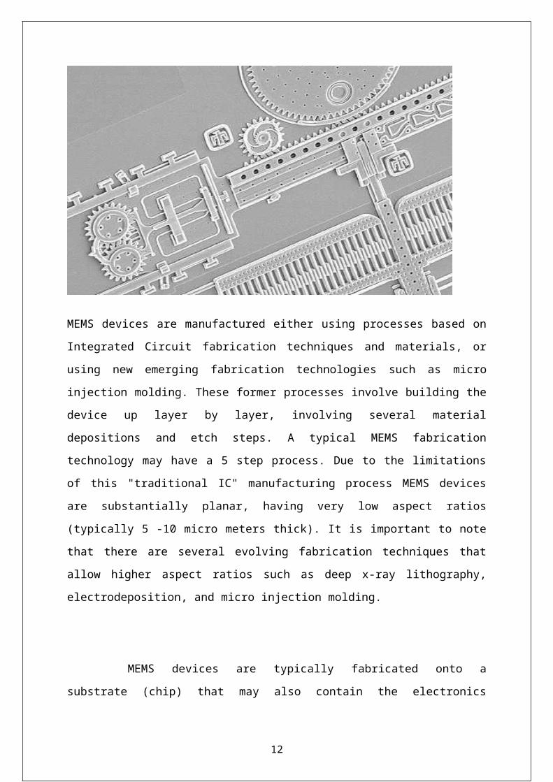
MICRO ELECTRO MECHANICAL SYSTEMS
Microelectromechanical systems (MEMS) are small integrated devices or
systems that combine electrical and mechanical components. They range in size from the sub
micrometer level to the millimeter level and there can be any number, from a few to millions,
in a particular system. MEMS extend the fabrication techniques developed for the integrated
circuit industry to add mechanical elements such as beams, gears, diaphragms, and springs to
devices.
Examples of MEMS device applications include inkjet-printer cartridges,
accelerometer, miniature robots, microengines, locks inertial sensors microtransmissions,
micromirrors, micro actuator (Mechanisms for activating process control equipment by use of
pneumatic, hydraulic, or electronic signals) optical scanners, fluid pumps, transducer,
pressure and flow sensors. New applications are emerging as the existing technology is
applied to the miniaturization and integration of conventional devices.
These systems can sense, control, and activate mechanical processes on the
micro scale, and function individually or in arrays to generate effects on the macro scale. The
micro fabrication technology enables fabrication of large arrays of devices, which
individually perform simple tasks, but in combination can accomplish complicated functions.
MEMS are not about any one application or device, nor are they defined by a
single fabrication process or limited to a few materials. They are a fabrication approach that
conveys the advantages of miniaturization, multiple components, and microelectronics to the
design and construction of integrated electromechanical systems. MEMS are not only about
miniaturization of mechanical systems; they are also a new paradigm for designing
mechanical devices and systems.
The MEMS industry has an estimated $10 billion market, and with a projected
10-20% annual growth rate, it is estimated to have a $34 billion market in 2002. Because of
the significant impact that MEMS can have on the commercial and defense markets, industry
and the federal government have both taken a special interest in their development.
8

WHAT IS MEMS TECHNOLOGY?
Micro-Electro-Mechanical Systems (MEMS) is the integration of mechanical
elements, sensors, actuators, and electronics on a common silicon substrate through
microfabrication technology. While the electronics are fabricated using integrated circuit (IC)
process sequences, the micromechanical components are fabricated using compatible
"micromachining" processes that selectively etch away parts of the silicon wafer or add new
structural layers to form the mechanical and electromechanical devices.
What are MEMS / Microsystems?
MEMS is an abbreviation for Micro Electro Mechanical Systems. This is a
rapidly emerging technology combining electrical, electronic, mechanical, optical, material,
chemical, and fluids engineering disciplines. As the smallest commercially produced
9
"machines", MEMS devices are similar to traditional sensors and actuators although much,
much smaller. E.g. Complete systems are typically a few millimeters across, with individual
features devices of the order of 1-100 micrometers across.
MEMS devices are manufactured either using processes based on Integrated Circuit
fabrication techniques and materials, or using new emerging fabrication technologies such as
micro injection molding. These former processes involve building the device up layer by
layer, involving several material depositions and etch steps. A typical MEMS fabrication
technology may have a 5 step process. Due to the limitations of this "traditional IC"
manufacturing process MEMS devices are substantially planar, having very low aspect ratios
(typically 5 -10 micro meters thick). It is important to note that there are several evolving
fabrication techniques that allow higher aspect ratios such as deep x-ray lithography,
electrodeposition, and micro injection molding.
MEMS devices are typically fabricated onto a substrate (chip) that may also
contain the electronics required to interact with the MEMS device. Due to the small size and
mass of the devices, MEMS components can be actuated electrostatically (piezoelectric and
bimetallic effects can also be used). The position of MEMS components can also be sensed
capacitively. Hence the MEMS electronics include electrostatic drive power supplies,
capacitance charge comparators, and signal conditioning circuitry. Connection with the
10

macroscopic world is via wire bonding and encapsulation into familiar BGA, MCM, surface
mount, or leaded IC packages.
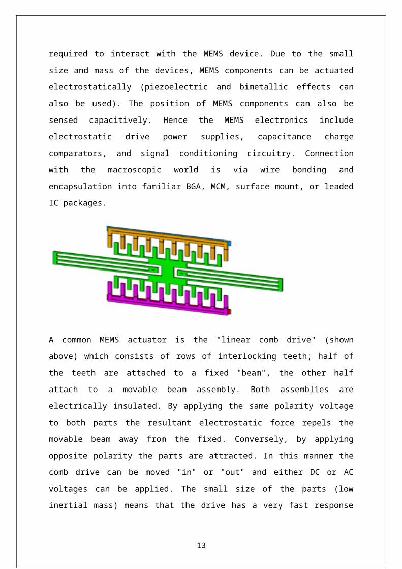
A common MEMS actuator is the "linear comb drive" (shown above) which consists of rows
of interlocking teeth; half of the teeth are attached to a fixed "beam", the other half attach to a
movable beam assembly. Both assemblies are electrically insulated. By applying the same
polarity voltage to both parts the resultant electrostatic force repels the movable beam away
from the fixed. Conversely, by applying opposite polarity the parts are attracted. In this
manner the comb drive can be moved "in" or "out" and either DC or AC voltages can be
applied. The small size of the parts (low inertial mass) means that the drive has a very fast
response time compared to its macroscopic counterpart. The magnitude of electrostatic force
is multiplied by the voltage or more commonly the surface area and number of teeth.
Commercial comb drives have several thousand teeth, each tooth approximately 10 micro
meters long. Drive voltages are CMOS levels.
The linear push / pull motion of a comb drive can be converted into rotational
motion by coupling the drive to push rod and pinion on a wheel. In this manner the comb
drive can rotate the wheel in the same way a steam engine functions!
11
Historical Background
The invention of the at Bell Telephone Laboratories in 1947 sparked a fast-
growing microelectronic technology. Jack Kilby of Texas Instruments built the first
Integrated circuit in 1958 using germanium (Ge) devices. It consisted of one transistor, three
Resistors, and one Capacitor. The IC was implemented on a sliver of Ge that was glued on a
glass slide. Later that same year Robert Noyce of Fairchild Semiconductor announced the
development of a Planar double-diffused Si IC. The complete transition from the original Ge
transistors with grown and alloyed junctions to silicon (Si) planar double-diffused devices
took about 10 years. The success of Si as an electronic material was due partly to its wide
availability from silicon dioxide (SiO2-sand), resulting in potentially lower material costs
relative to other Semiconductors
Since 1970, the complexity of ICs has doubled every two to three years. The
minimum dimension of manufactured devices and ICs has decreased from 20 microns to the
sub micron levels of today. Current ultra-large-scale-integration (ULSI) technology enables
the fabrication of more than 10 million transistors and capacitors on a typical chip.
IC fabrication is dependent upon sensors to provide input from the surrounding
environment, just as control systems need actuators in order to carry out their desired
functions. Due to the availability of sand as a material, much effort was put into developing
Si processing and characterization tools. These tools are now being used to advance
transducer technology. Today's IC technology far outstrips the original sensors and actuators
in performance, size, and cost.
Around 1982, the term micromachining came into use to designate the
fabrication of micromechanical parts for Si microsensors. The micromechanical parts were
fabricated by selectively etching areas of the Si substrate away in order to leave behind the
desired geometries. Isotropic etching of Si was developed in the early 1960s for transistor
fabrication. Anisotropic etching of Si then came about in 1967. Various etch-stop techniques
were subsequently developed to provide further process flexibility.
These techniques also form the basis of the bulk micromachining processing
techniques. Bulk micromachining designates the point at which the bulk of the Si substrate is
etched away to leave behind the desired micromechanical elements. Bulk micromachining
12
has remained a powerful technique for the fabrication of micromechanical elements.
However, the need for flexibility in device design and performance improvement has
motivated the development of new concepts and techniques for micromachining.
Among these is the sacrificial layer technique, first demonstrated in 1965 by
Nathanson and Wickstrom, in which a layer of material is deposited between structural layers
for mechanical separation and isolation. This layer is removed during the release etch to free
the structural layers and to allow mechanical devices to move relative to the substrate. A
layer is releasable when a sacrificial layer separates it from the substrate. The application of
the sacrificial layer technique to micromachining in 1985 gave rise to surface
micromachining, in which the Si substrate is primarily used as a mechanical support upon
which the micromechanical elements are fabricated.
Prior to 1987, these micromechanical structures were limited in motion. During
1987-1988, a turning point was reached in micromachining when, for the first time,
techniques for integrated fabrication of mechanisms on Si were demonstrated. During a series
of three separate workshops on microdynamics held in 1987, the term MEMS was coined.
Equivalent terms for MEMS are microsystems-preferred in Europe and micromachines-
preferred in Japan.
MEMS DESCRIPTION
MEMS technology can be implemented using a number of different materials
and manufacturing techniques; the choice of which will depend on the device being created
and the market sector in which it has to operate.
SILICON
The economies of scale, ready availability of cheap high-quality materials and
ability to incorporate electronic functionality make silicon attractive for a wide variety of
MEMS applications. Silicon also has significant advantages engendered through its material
properties. In single crystal form, silicon is an almost perfect Hookean material, meaning that
when it is flexed there is virtually no hysteresis and hence almost no energy dissipation. The
basic techniques for producing all silicon based MEMS devices are deposition of material
13
layers, patterning of these layers by photolithography and then etching to produce the
required shapes.
POLYMERS
Even though the electronics industry provides an economy of scale for the
silicon industry, crystalline silicon is still a complex and relatively expensive material to
produce. Polymers on the other hand can be produced in huge volumes, with a great variety
of material characteristics. MEMS devices can be made from polymers by processes such as
injection moulding, embossing or stereolithography and are especially well suited to
microfluidic applications such as disposable blood testing cartridges.
METALS
Metals can also be used to create MEMS elements. While metals do not have
some of the advantages displayed by silicon in terms of mechanical properties, when used
within their limitations, metals can exhibit very high degrees of reliability. Metals can be
deposited by electroplating, evaporation, and sputtering processes. Commonly used metals
include gold, nickel, aluminum, chromium, titanium, tungsten, platinum, and silver.
MEMS DESIGN PROCESS
There are three basic building blocks in MEMS technology, which are,
Deposition Process-the ability to deposit thin films of material on a substrate, Lithography-
to apply a patterned mask on top of the films by photolithograpic imaging, and Etching-to
etch the films selectively to the mask. A MEMS process is usually a structured sequence of
these operations to form actual devices.
14

Deposition ProcessesOne of the basic building blocks in MEMS processing is the ability to deposit
thin films of material. In this text we assume a thin film to have a thickness anywhere
between a few nanometers to about 100 micrometer
MEMS deposition technology can be classified in two groups:
1. Depositions that happen because of a chemical reaction:
o Chemical Vapor Deposition (CVD)
o Electrodeposition
o Epitaxy
o Thermal oxidation
These processes exploit the creation of solid materials directly from chemical
reactions in gas and/or liquid compositions or with the substrate material. The solid
material is usually not the only product formed by the reaction. Byproducts can
include gases, liquids and even other solids.
2. Depositions that happen because of a physical reaction:
o Physical Vapor Deposition (PVD)
o Casting
Common for all these processes are that the material deposited is physically moved on
to the substrate. In other words, there is no chemical reaction which forms the
material on the substrate. This is not completely correct for casting processes, though
it is more convenient to think of them that way.
This is by no means an exhaustive list since technologies evolve continuously.
Chemical Vapor Deposition (CVD) :
In this process, the substrate is placed inside a reactor to which a number of
gases are supplied. The fundamental principle of the process is that a chemical reaction takes
place between the source gases. The product of that reaction is a solid material with
condenses on all surfaces inside the reactor.
15
The two most important CVD technologies in MEMS are the Low Pressure
CVD (LPCVD) and Plasma Enhanced CVD (PECVD). The LPCVD process produces layers
with excellent uniformity of thickness and material characteristics. The main problems with
the process are the high deposition temperature (higher than 600°C) and the relatively slow
deposition rate. The PECVD process can operate at lower temperatures (down to 300° C)
thanks to the extra energy supplied to the gas molecules by the plasma in the reactor.
However, the quality of the films tend to be inferior to processes running at higher
temperatures. Secondly, most PECVD deposition systems can only deposit the material on
one side of the wafers on 1 to 4 wafers at a time. LPCVD systems deposit films on both sides
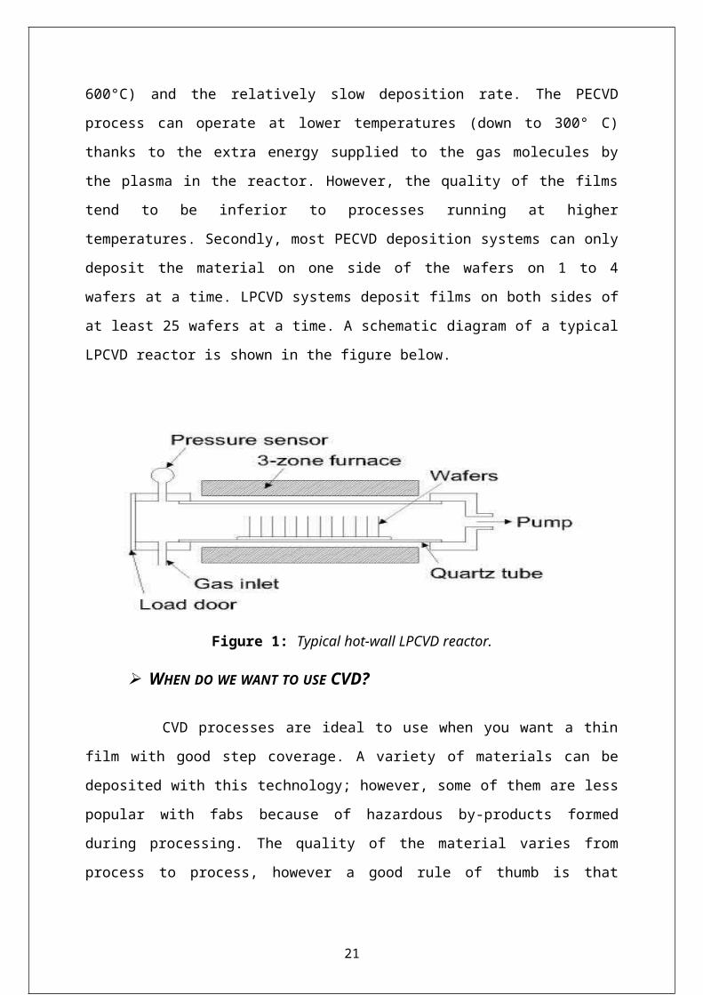
of at least 25 wafers at a time. A schematic diagram of a typical LPCVD reactor is shown in
the figure below.
Figure 1: Typical hot-wall LPCVD reactor.
WHEN DO WE WANT TO USE CVD?
CVD processes are ideal to use when you want a thin film with good step
coverage. A variety of materials can be deposited with this technology; however, some of
them are less popular with fabs because of hazardous by-products formed during processing.
The quality of the material varies from process to process, however a good rule of thumb is
that higher process temperature yields a material with higher quality and less defects.
16
ELECTRODEPOSITION:
This process is also known as "electroplating" and is typically restricted to
electrically conductive materials. There are basically two technologies for plating:
Electroplating and Electroless plating. In the electroplating process the substrate is placed in a
liquid solution (electrolyte). When an electrical potential is applied between a conducting
area on the substrate and a counter electrode (usually platinum) in the liquid, a chemical
redox process takes place resulting in the formation of a layer of material on the substrate and
usually some gas generation at the counter electrode.
In the electroless plating process a more complex chemical solution is used, in
which deposition happens spontaneously on any surface which forms a sufficiently high
electrochemical potential with the solution. This process is desirable since it does not require
any external electrical potential and contact to the substrate during processing. Unfortunately,
it is also more difficult to control with regards to film thickness and uniformity. A schematic
diagram of a typical setup for electroplating is shown in the figure below.
WHEN DO W11E WANT TO USE ELECTRODEPOSITION?
The electrodeposition process is well suited to make films of metals such as
copper, gold and nickel. The films can be made in any thickness from ~1µm to >100µm. The
deposition is best controlled when used with an external electrical potential, however, it
requires electrical contact to the substrate when immersed in the liquid bath. In any process,
the surface of the substrate must have an electrically conducting coating before the deposition
can be done.
17
Figure 2: Typical setup for electrodeposition.
EPITAXY:
This technology is quite similar to what happens in CVD processes, however, if
the substrate is an ordered semiconductor crystal (i.e. silicon, gallium arsenide), it is possible
with this process to continue building on the substrate with the same crystallographic
orientation with the substrate acting as a seed for the deposition. If an
amorphous/polycrystalline substrate surface is used, the film will also be amorphous or
polycrystalline.
There are several technologies for creating the conditions inside a reactor
needed to support epitaxial growth, of which the most important is Vapor Phase Epitaxy
(VPE). In this process, a number of gases are introduced in an induction heated reactor where
only the substrate is heated. The temperature of the substrate typically must be at least 50%
of the melting point of the material to be deposited.
An advantage of epitaxy is the high growth rate of material, which allows the
formation of films with considerable thickness (>100µm). Epitaxy is a widely used
technology for producing silicon on insulator (SOI) substrates. The technology is primarily
used for deposition of silicon. A schematic diagram of a typical vapor phase epitaxial reactor
is shown in the figure below.
18
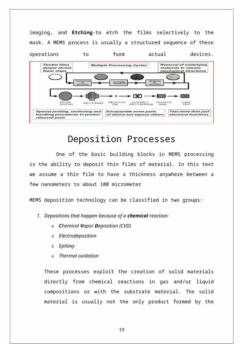
Figure 3: Typical cold-wall vapor phase epitaxial reactor.
WHEN DO WE WANT TO USE EPITAXY?
This has been and continues to be an emerging process technology in MEMS.
The process can be used to form films of silicon with thicknesses of ~1µm to >100µm. Some
processes require high temperature exposure of the substrate, whereas others do not require
significant heating of the substrate. Some processes can even be used to perform selective
deposition, depending on the surface of the substrate.
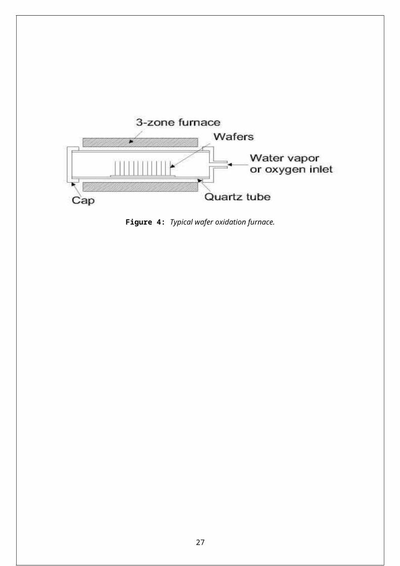
THERMAL OXIDATION:
This is one of the most basic deposition technologies. It is simply oxidation of
the substrate surface in an oxygen rich atmosphere. The temperature is raised to 800° C-
1100° C to speed up the process. This is also the only deposition technology which actually
consumes some of the substrate as it proceeds. The growth of the film is spurned by diffusion
of oxygen into the substrate, which means the film growth is actually downwards into the
substrate. As the thickness of the oxidized layer increases, the diffusion of oxygen to the
substrate becomes more difficult leading to a parabolic relationship between film thickness
and oxidation time for films thicker than ~100nm. This process is naturally limited to
materials that can be oxidized, and it can only form films that are oxides of that material. This
19
is the classical process used to form silicon dioxide on a silicon substrate. A schematic
diagram of a typical wafer oxidation furnace is shown in the figure below.
WHEN DO WE WANT TO USE THERMAL OXIDATION?
Whenever you can! This is a simple process, which unfortunately produces
films with somewhat limited use in MEMS components. It is typically used to form films that
are used for electrical insulation or that are used for other process purposes later in a process
sequence.
Figure 4: Typical wafer oxidation furnace.
20
Physical Vapor Deposition (PVD) :
PVD covers a number of deposition technologies in which material is released
from a source and transferred to the substrate. The two most important technologies are
evaporation and sputtering.
WHEN DO WE WANT TO USE PVD?
PVD comprises the standard technologies for deposition of metals. It is far
more common than CVD for metals since it can be performed at lower process risk and
cheaper in regards to materials cost. The quality of the films are inferior to CVD, which for
metals means higher resistivity and for insulators more defects and traps. The step coverage
is also not as good as CVD.
The choice of deposition method (i.e. evaporation vs. sputtering) may in many
cases be arbitrary, and may depend more on what technology is available for the specific
material at the time.
EVAPORATION:
In evaporation the substrate is placed inside a vacuum chamber, in which a
block (source) of the material to be deposited is also located. The source material is then
heated to the point where it starts to boil and evaporate. The vacuum is required to allow the
molecules to evaporate freely in the chamber, and they subsequently condense on all
surfaces. This principle is the same for all evaporation technologies, only the method used to
the heat (evaporate) the source material differs. There are two popular evaporation
technologies, which are e-beam evaporation and resistive evaporation each referring to the
heating method. In e-beam evaporation, an electron beam is aimed at the source material
causing local heating and evaporation. In resistive evaporation, a tungsten boat, containing
the source material, is heated electrically with a high current to make the material evaporate.
Many materials are restrictive in terms of what evaporation method can be used (i.e.
aluminum is quite difficult to evaporate using resistive heating), which typically relates to the
21
phase transition properties of that material. A schematic diagram of a typical system for e-
beam evaporation is shown in the figure below.
Figure 5: Typical system for e-beam evaporation of materials.
SPUTTERING:
Sputtering is a technology in which the material is released from the source at
much lower temperature than evaporation. The substrate is placed in a vacuum chamber with
the source material, named a target, and an inert gas (such as argon) is introduced at low
pressure. Gas plasma is struck using an RF power source, causing the gas to become ionized.
The ions are accelerated towards the surface of the target, causing atoms of the source
material to break off from the target in vapor form and condense on all surfaces including the
substrate. As for evaporation, the basic principle of sputtering is the same for all sputtering
technologies. The differences typically relate to the manor in which the ion bombardment of
the target is realized. A schematic diagram of a typical RF sputtering system is shown in the
figure below.
22

Figure 6: Typical RF sputtering system.
CASTING:
In this process the material to be deposited is dissolved in liquid form in a
solvent. The material can be applied to the substrate by spraying or spinning. Once the
solvent is evaporated, a thin film of the material remains on the substrate. This is particularly
useful for polymer materials, which may be easily dissolved in organic solvents, and it is the
common method used to apply photoresist to substrates (in photolithography). The
thicknesses that can be cast on a substrate range all the way from a single monolayer of
molecules (adhesion promotion) to tens of micrometers. In recent years, the casting
technology has also been applied to form films of glass materials on substrates. The spin
casting process is illustrated in the figure below.
Figure 7: The spin casting process as used for photoresist in photolithography.
23
Lithography
Pattern Transfer:
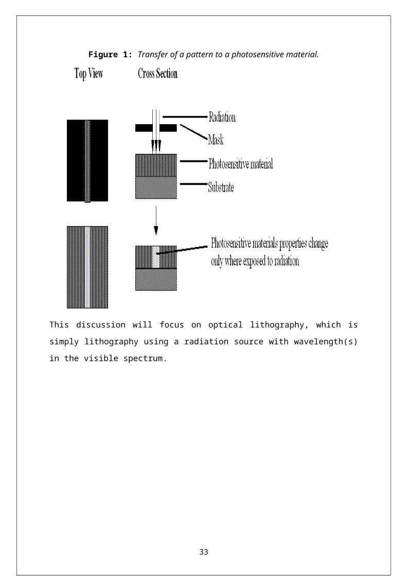
Lithography in the MEMS context is typically the transfer of a pattern to a
photosensitive material by selective exposure to a radiation source such as light. A
photosensitive material is a material that experiences a change in its physical properties when
exposed to a radiation source. If we selectively expose a photosensitive material to radiation
(e.g. by masking some of the radiation) the pattern of the radiation on the material is
transferred to the material exposed, as the properties of the exposed and unexposed regions
differs (as shown in figure 1).
In lithography for micromachining, the photosensitive material used is typically
a photoresist (also called resist, other photosensitive polymers are also used). When resist is
exposed to a radiation source of a specific a wavelength, the chemical resistance of the resist
to developer solution changes. If the resist is placed in a developer solution after selective
exposure to a light source, it will etch away one of the two regions (exposed or unexposed). If
the exposed material is etched away by the developer and the unexposed region is resilient,
the material is considered to be a positive resist (shown in figure 2a). If the exposed material
is resilient to the developer and the unexposed region is etched away, it is considered to be a
negative resist (shown in figure 2b).
24
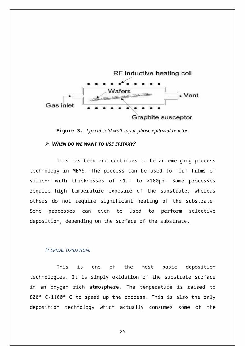
Figure 1: Transfer of a pattern to a photosensitive material.
This discussion will focus on optical lithography, which is simply lithography using a
radiation source with wavelength(s) in the visible spectrum.
25

Figure 2: a) Pattern definition in positive resist, b) Pattern definition in negative resist.
Lithography is the principal mechanism for pattern definition in
micromachining. Photosensitive compounds are primarily organic, and do not encompass the
spectrum of materials properties of interest to micro-machinists. However, as the technique is
capable of producing fine features in an economic fashion, a photosensitive layer is often
used as a temporary mask when etching an underlying layer, so that the pattern may be
transferred to the underlying layer (shown in figure 3a). Photoresist may also be used as a
template for patterning material deposited after lithography (shown in figure 3b). The resist is
subsequently etched away, and the material deposited on the resist is "lifted off".
The deposition template (lift-off) approach for transferring a pattern from resist
to another layer is less common than using the resist pattern as an etch mask. The reason for
26
this is that resist is incompatible with most MEMS deposition processes, usually because it
cannot withstand high temperatures and may act as a source of contamination.
Figure 3: a) Pattern transfer from patterned photoresist to underlying layer by etching, b) Pattern transfer from patterned photoresist to overlying layer by lift-off.
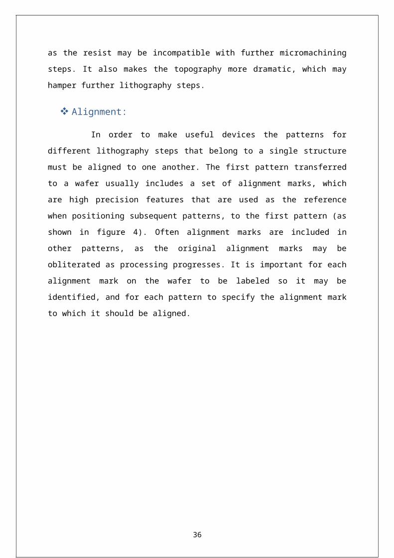
Once the pattern has been transferred to another layer, the resist is usually
stripped. This is often necessary as the resist may be incompatible with further
micromachining steps. It also makes the topography more dramatic, which may hamper
further lithography steps.
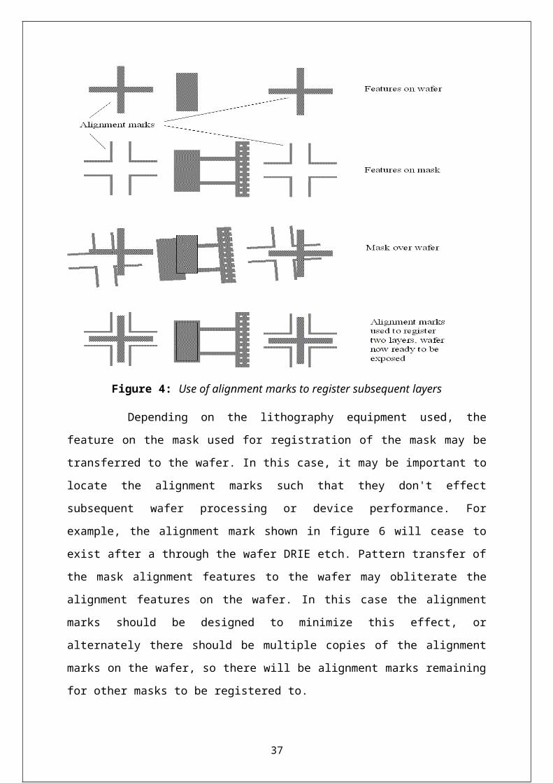
Alignment:
In order to make useful devices the patterns for different lithography steps that
belong to a single structure must be aligned to one another. The first pattern transferred to a
wafer usually includes a set of alignment marks, which are high precision features that are
used as the reference when positioning subsequent patterns, to the first pattern (as shown in
figure 4). Often alignment marks are included in other patterns, as the original alignment
marks may be obliterated as processing progresses. It is important for each alignment mark
on the wafer to be labeled so it may be identified, and for each pattern to specify the
alignment mark to which it should be aligned.
27
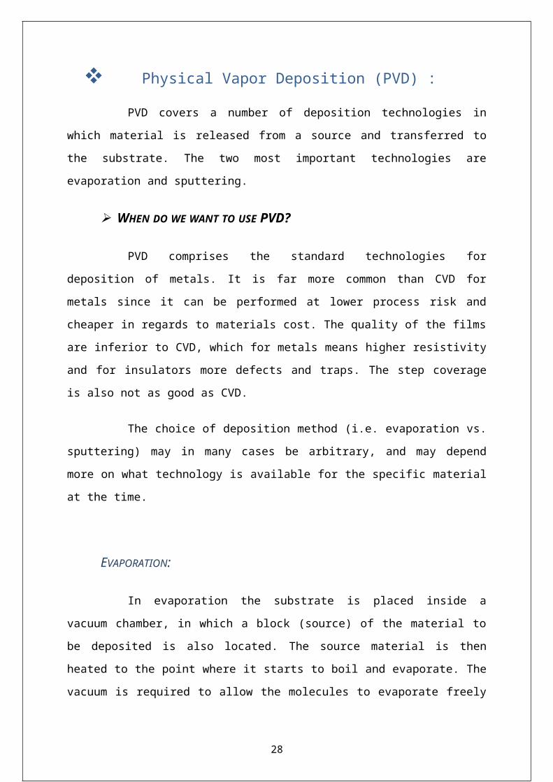
Figure 4: Use of alignment marks to register subsequent layers
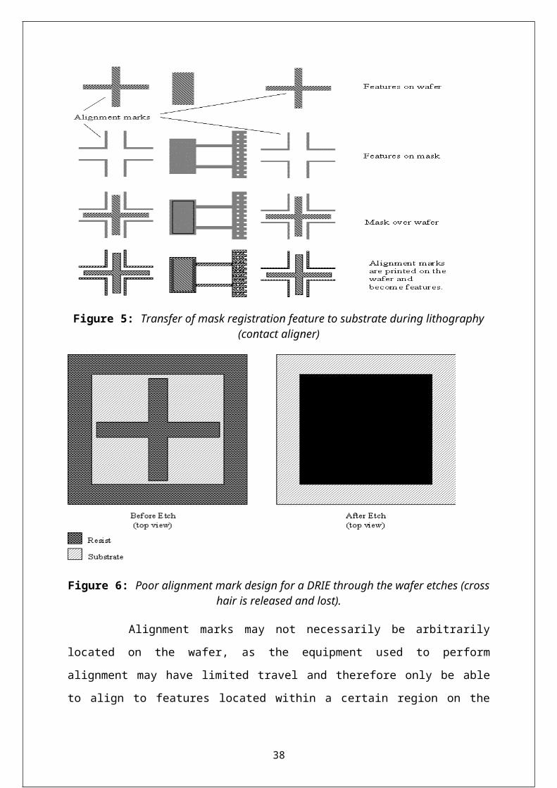
Depending on the lithography equipment used, the feature on the mask used for
registration of the mask may be transferred to the wafer. In this case, it may be important to
locate the alignment marks such that they don't effect subsequent wafer processing or device
performance. For example, the alignment mark shown in figure 6 will cease to exist after a
through the wafer DRIE etch. Pattern transfer of the mask alignment features to the wafer
may obliterate the alignment features on the wafer. In this case the alignment marks should
be designed to minimize this effect, or alternately there should be multiple copies of the
alignment marks on the wafer, so there will be alignment marks remaining for other masks to
be registered to.
28
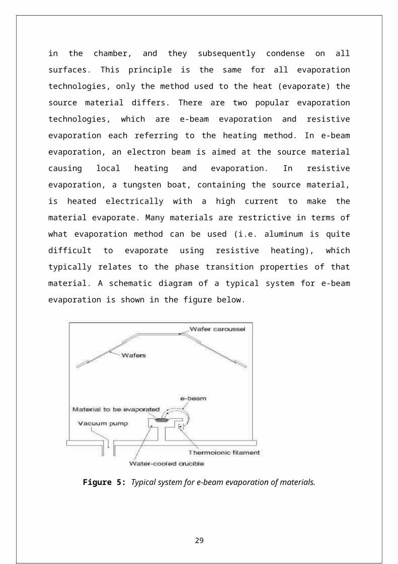
Figure 5: Transfer of mask registration feature to substrate during lithography (contact aligner)
Figure 6: Poor alignment mark design for a DRIE through the wafer etches (cross hair is released and lost).
Alignment marks may not necessarily be arbitrarily located on the wafer, as the
equipment used to perform alignment may have limited travel and therefore only be able to
align to features located within a certain region on the wafer (as shown in figure 7). The
region location geometry and size may also vary with the type of alignment, so the
lithographic equipment and type of alignment to be used should be considered before locating
29

alignment marks. Typically two alignment marks are used to align the mask and wafer, one
alignment mark is sufficient to align the mask and wafer in x and y, but it requires two marks
(preferably spaced far apart) to correct for fine offset in rotation.
As there is no pattern on the wafer for the first pattern to align to, the first
pattern is typically aligned to the primary wafer flat (as shown in figure 8). Depending on the
lithography equipment used, this may be done automatically, or by manual alignment to an
explicit wafer registration feature on the mask
Figure 7: Restriction of location of alignment marks based on equipment used.
.
30

Figure 8: Mask alignment to the wafer flat.
Exposure:
The exposure parameters required in order to achieve accurate pattern transfer
from the mask to the photosensitive layer depend primarily on the wavelength of the radiation
source and the dose required to achieve the desired properties change of the photoresist.
Different photoresists exhibit different sensitivities to different wavelengths. The dose
required per unit volume of photoresist for good pattern transfer is somewhat constant;
however, the physics of the exposure process may affect the dose actually received. For
example a highly reflective layer under the photoresist may result in the material
experiencing a higher dose than if the underlying layer is absorptive, as the photoresist is
exposed both by the incident radiation as well as the reflected radiation. The dose will also
vary with resist thickness.
There are also higher order effects, such as interference patterns in thick resist
films on reflective substrates, which may affect the pattern transfer quality and sidewall
properties.
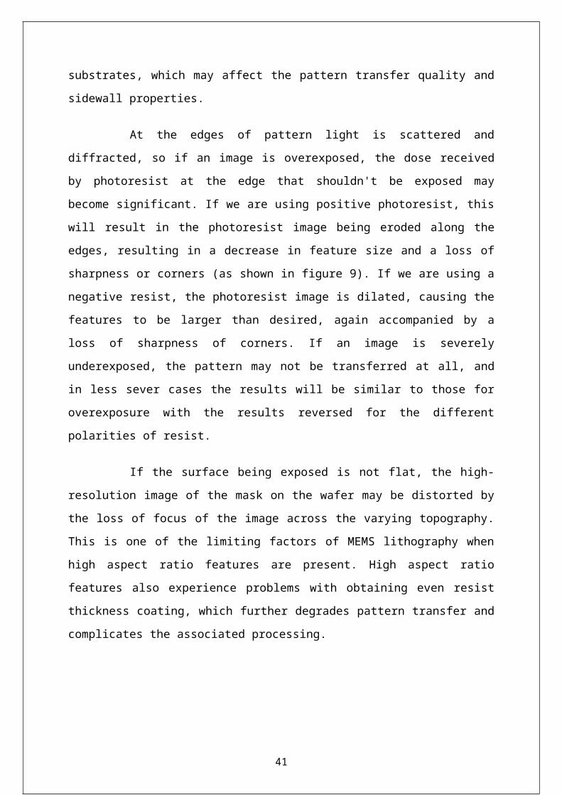
At the edges of pattern light is scattered and diffracted, so if an image is
overexposed, the dose received by photoresist at the edge that shouldn't be exposed may
become significant. If we are using positive photoresist, this will result in the photoresist
image being eroded along the edges, resulting in a decrease in feature size and a loss of
sharpness or corners (as shown in figure 9). If we are using a negative resist, the photoresist
image is dilated, causing the features to be larger than desired, again accompanied by a loss
of sharpness of corners. If an image is severely underexposed, the pattern may not be
transferred at all, and in less sever cases the results will be similar to those for overexposure
with the results reversed for the different polarities of resist.
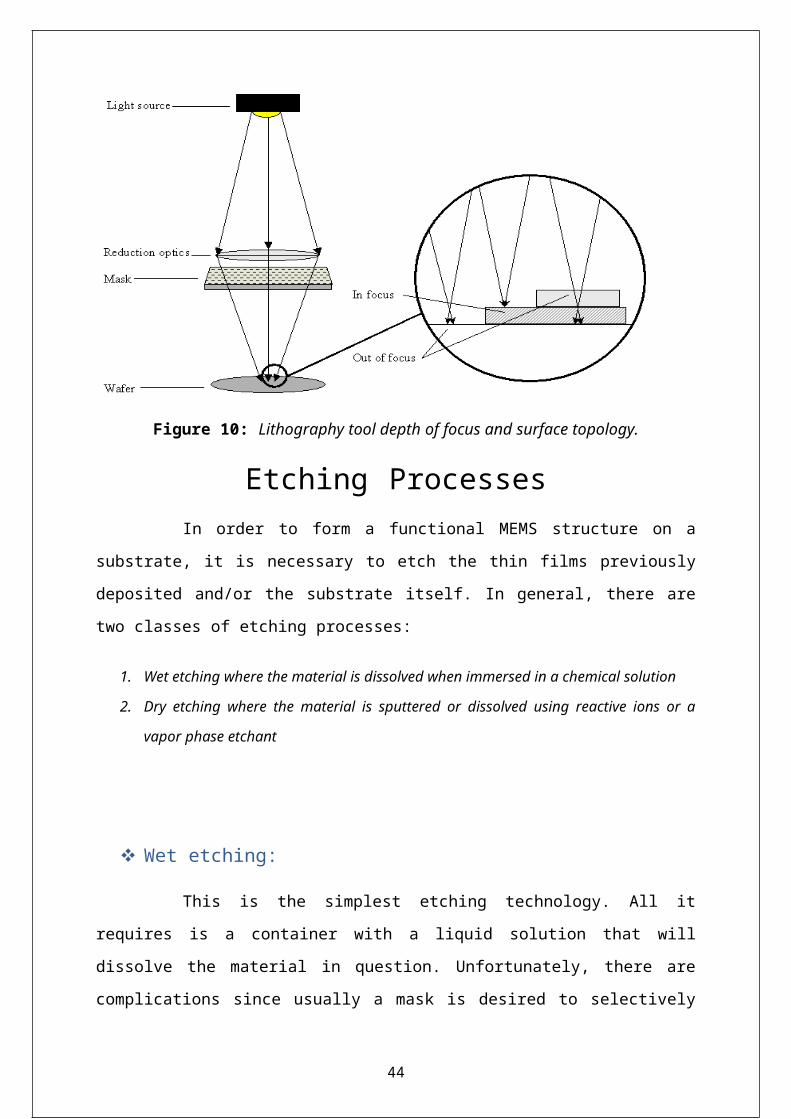
If the surface being exposed is not flat, the high-resolution image of the mask
on the wafer may be distorted by the loss of focus of the image across the varying
topography. This is one of the limiting factors of MEMS lithography when high aspect ratio
features are present. High aspect ratio features also experience problems with obtaining even
resist thickness coating, which further degrades pattern transfer and complicates the
associated processing.
31

Figure 9: Over and under-exposure of positive resist.
The Lithography Module:
Typically lithography is performed as part of a well-characterized module,
which includes the wafer surface preparation, photoresist deposition, alignment of the mask
and wafer, exposure, develop and appropriate resist conditioning. The lithography process
steps need to be characterized as a sequence in order to ensure that the remaining resist at the
end of the modules is an optimal image of the mask, and has the desired sidewall profile.
A brief explanation of the standard process steps included in a lithography
module is (in sequence):
Dehydration bake - dehydrate the wafer to aid resist adhesion.
HMDS prime - coating of wafer surface with adhesion promoter.
Resist spin/spray - coating of the wafer with resist either by spinning or
spraying. Typically desire a uniform coat.
32
Soft bake - drive off some of the solvent in the resist, may result in a
significant loss of mass of resist (and thickness). Makes resist more
viscous.
Alignment - align pattern on mask to features on wafers.
Exposure - projection of mask image on resist causing selective chemical
property change.
Post exposure bake - baking of resist to drive off further solvent
content.
Develop - selective removal of resist after exposure. Usually a wet
process.
Hard bake - drive off most of the remaining solvent from the resist.
Descum - removal of thin layer of resist scum that may occlude open
regions in pattern helps to open up corners.
We make a few assumptions about photolithography. Firstly, we assume that a
well characterized module exists that: prepares the wafer surface, deposits the requisite resist
thickness, aligns the mask perfectly, exposes the wafer with the optimal dosage, develops the
resist under the optimal conditions, and bakes the resist for the appropriate times at the
appropriate locations in the sequence. Unfortunately, even if the module is executed
perfectly, the properties of lithography are very feature and topography dependent. It is
therefore necessary for the designer to be aware of certain limitations of lithography, as well
as the information they should provide to the technician performing the lithography.
33
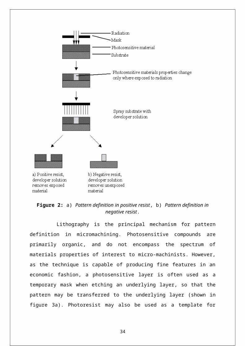
Figure 10: Lithography tool depth of focus and surface topology.
Etching ProcessesIn order to form a functional MEMS structure on a substrate, it is necessary to
etch the thin films previously deposited and/or the substrate itself. In general, there are two
classes of etching processes:
1. Wet etching where the material is dissolved when immersed in a chemical solution
2. Dry etching where the material is sputtered or dissolved using reactive ions or a vapor phase
etchant
Wet etching:
This is the simplest etching technology. All it requires is a container with a
liquid solution that will dissolve the material in question. Unfortunately, there are
complications since usually a mask is desired to selectively etch the material. One must find a
mask that will not dissolve or at least etches much slower than the material to be patterned.
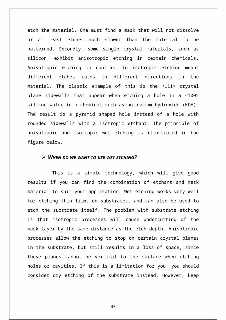
Secondly, some single crystal materials, such as silicon, exhibit anisotropic etching in certain
chemicals. Anisotropic etching in contrast to isotropic etching means different etches rates in
different directions in the material. The classic example of this is the <111> crystal plane
sidewalls that appear when etching a hole in a <100> silicon wafer in a chemical such as
potassium hydroxide (KOH). The result is a pyramid shaped hole instead of a hole with
rounded sidewalls with a isotropic etchant. The principle of anisotropic and isotropic wet
etching is illustrated in the figure below.
WHEN DO WE WANT TO USE WET ETCHING?
This is a simple technology, which will give good results if you can find the
combination of etchant and mask material to suit your application. Wet etching works very
well for etching thin films on substrates, and can also be used to etch the substrate itself. The
problem with substrate etching is that isotropic processes will cause undercutting of the mask
layer by the same distance as the etch depth. Anisotropic processes allow the etching to stop
on certain crystal planes in the substrate, but still results in a loss of space, since these planes
34

cannot be vertical to the surface when etching holes or cavities. If this is a limitation for you,
you should consider dry etching of the substrate instead. However, keep in mind that the cost
per wafer will be 1-2 orders of magnitude higher to perform the dry etching
If you are making very small features in thin films (comparable to the film
thickness), you may also encounter problems with isotropic wet etching, since the
undercutting will be at least equal to the film thickness. With dry etching it is possible etch
almost straight down without undercutting, which provides much higher resolution.
Figure 1: Difference between anisotropic and isotropic wet etching.
Dry etching:
The dry etching technology can split in three separate classes called reactive ion
etching (RIE), sputter etching, and vapor phase etching.
In RIE, the substrate is placed inside a reactor in which several gases are
introduced. Plasma is struck in the gas mixture using an RF power source, breaking the gas
molecules into ions. The ion is accelerated towards, and reacts at, the surface of the material
being etched, forming another gaseous material. This is known as the chemical part of
reactive ion etching. There is also a physical part which is similar in nature to the sputtering
deposition process. If the ions have high enough energy, they can knock atoms out of the
material to be etched without a chemical reaction. It is very complex tasks to develop dry
etch processes that balance chemical and physical etching, since there are many parameters to
adjust. By changing the balance it is possible to influence the anisotropy of the etching, since
the chemical part is isotropic and the physical part highly anisotropic the combination can
35
form sidewalls that have shapes from rounded to vertical. A schematic of a typical reactive
ion etching system is shown in the figure below.
A special subclass of RIE which continues to grow rapidly in popularity is deep
RIE (DRIE). In this process, etch depths of hundreds of microns can be achieved with almost
vertical sidewalls. The primary technology is based on the so-called "Bosch process", named
after the German company Robert Bosch which filed the original patent, where two different
gas compositions are alternated in the reactor. The first gas composition creates a polymer on
the surface of the substrate, and the second gas composition etches the substrate. The polymer
is immediately sputtered away by the physical part of the etching, but only on the horizontal
surfaces and not the sidewalls. Since the polymer only dissolves very slowly in the chemical
part of the etching, it builds up on the sidewalls and protects them from etching. As a result,
etching aspect ratios of 50 to 1 can be achieved. The big difference is that substrate is now
subjected to the ion bombardment instead of the material target used in sputter deposition.
WHEN DO WE WANT TO USE DRY ETCHING?
The first thing you should note about this technology is that it is expensive to
run compared to wet etching. If you are concerned with feature resolution in thin film
structures or you need vertical sidewalls for deep etchings in the substrate, you have to
consider dry etching. If you are concerned about the price of your process and device, you
may want to minimize the use of dry etching. The IC industry has long since adopted dry
etching to achieve small features, but in many cases feature size is not as critical in MEMS.
Dry etching is an enabling technology, which comes at a sometimes high cost.
Figure 2: Typical parallel-plate reactive ion etching system.
36
Fabrication TechnologiesThe three characteristic features of MEMS fabrication technologies are
miniaturization, multiplicity, and microelectronics. Miniaturization enables the production of
compact, quick-response devices. Multiplicity refers to the batch fabrication inherent in
semiconductor processing, which allows thousands or millions of components to be easily
and concurrently fabricated. Microelectronics provides the intelligence to MEMS and allows
the monolithic merger of sensors, actuators, and logic to build closed-loop feedback
components and systems. The successful miniaturization and multiplicity of traditional
electronics systems would not have been possible without IC fabrication technology.
Therefore, IC fabrication technology, or microfabrication, has so far been the primary
enabling technology for the development of MEMS. Microfabrication provides a powerful
tool for batch processing and miniaturization of mechanical systems into a dimensional
domain not accessible by conventional techniques. Furthermore, microfabrication provides an
opportunity for integration of mechanical systems with electronics to develop high-
performance closed-loop-controlled MEMS.
IC Fabrication:
Any discussion of MEMS requires a basic understanding of IC fabrication
technology, or microfabrication, the primary enabling technology for the development of
MEMS. The major steps in IC fabrication technology are:
Film growth: Usually, a polished Si wafer is used as the substrate, on which a thin
film is grown. The film, which may be epitaxial Si, SiO2, silicon nitride (Si3N4),
polycrystalline Si, or metal, is used to build both active or passive components and
interconnections between circuits.
Doping: To modulate the properties of the device layer, a low and controllable level
of an atomic impurity may be introduced into the layer by thermal diffusion or ion
implantation.
Lithography: A pattern on a mask is then transferred to the film by means of a
photosensitive (i.e., light sensitive) chemical known as a photoresist. The process of
pattern generation and transfer is called photolithography. A typical mask consists of
a glass plate coated with a patterned chromium (Cr) film.
37
Etching: Next is the selective removal of unwanted regions of a film or substrate for
pattern delineation. Wet chemical etching or dry etching may be used. Etch-mask
materials are used at various stages in the removal process to selectively prevent those
portions of the material from being etched. These materials include SiO2, Si3N4, and
hard-baked photoresist.
Dicing: The finished wafer is sawed or machined into small squares, or dice, from
which electronic components can be made.
Packaging: The individual sections are then packaged, a process that involves
physically locating, connecting, and protecting a device or component. MEMS design
is strongly coupled to the packaging requirements, which in turn are dictated by the
application environment.
Bulk Micromachining and Wafer Bonding:
Bulk micromachining is an extension of IC technology for the fabrication of 3D
structures. Bulk micromachining of Si uses wet- and dry-etching techniques in conjunction
with etch masks and etch stops to sculpt micromechanical devices from the Si substrate. The
two key capabilities that make bulk micromachining a viable technology are:
38

Anisotropic etchants of Si, such as ethylene-diamine and pyrocatechol (EDP),
potassium hydroxide (KOH), and hydrazine (N2H4). These preferentially etch single
crystal Si along given crystal planes.
Etch masks and etch-stop techniques that can be used with Si anisotropic etchants to
selectively prevent regions of Si from being etched. Good etch masks are provided by
SiO2 and Si3N4, and some metallic thin films such as Cr and Au (gold).
A drawback of wet anisotropic etching is that the microstructure geometry is
defined by the internal crystalline structure of the substrate. Two additional processing
techniques have extended the range of traditional bulk micromachining technology: deep
anisotropic dry etching and wafer bonding. The other technology, wafer bonding, permits a Si
substrate to be attached to another substrate, typically Si or glass
Surface Micromachining:
Surface micromachining enables the fabrication of complex multicomponent
integrated micromechanical structures that would not be possible with traditional bulk
micromachining. This technique encases specific structural parts of a device in layers of a
sacrificial material during the fabrication process. The substrate wafer is used primarily as a
mechanical support on which multiple alternating layers of structural and sacrificial material
are deposited and patterned to realize micromechanical structures. The sacrificial material is
then dissolved in a chemical etchant that does not attack the structural parts. The most widely
used surface micromachining technique, polysilicon surface micromachining, uses SiO2 as
the sacrificial material and polysilicon as the structural material.
At the University of Wisconsin at Madison, polysilicon surface micromachining
research started in the early 1980s in an effort to create high-precision micro pressure
sensors. The control of the internal stresses of a thin film is important for the fabrication of
microelectromechanical structures. The microelectronic fabrication industry typically grows
polysilicon, silicon nitride, and silicon dioxide films using recipes that minimize time.
Unfortunately, a deposition process that is optimized to speed does not always create a low
internal stress film. In fact, most of these films have internal stresses that are highly
compressive. A freestanding plate of highly compressive polysilicon that is held at all its
edges will buckle. This is highly undesirable. The solution is to modify the film deposition
process to control the internal stress by making it stress-free or slightly tensile.
39

Micro molding:
In the micromolding process, microstructures are fabricated using molds to
define the deposition of the structural layer. The structural material is deposited only in those
areas constituting the microdevice structure, in contrast to bulk and surface micromachining,
which feature blanket deposition of the structural material followed by etching to realize the
final device geometry. After the structural layer deposition, the mold is dissolved in a
chemical etchant that does not attack the structural material. One of the most prominent
micromolding processes is the LIGA process. LIGA is a German acronym standing for
lithographie, galvanoformung, und abformung (lithography, electroplating, and molding).
This process can be used for the manufacture of high-aspect-ratio 3D microstructures in a
wide variety of materials, such as metals, polymers, ceramics, and glasses. Photosensitive
polyimides are also used for fabricating plating molds. The photolithography process is
similar to conventional photolithography, except that polyimide works as a negative resist.
Example: An insulin pump fabricated by classic MEMS technology
1. PUMPING MEMBRANE 2. PUMPING CHAMBER
3. INLET 4. OUTLET
5. LARGE MESA 6. UPPER GLASS PLATE
7. BOTTOM GLASS PLATE 8. PATTERNED THIN LAYER
40
Current ChallengesMEMS and Nanotechnology is currently used in low- or medium-volume
applications. Some of the obstacles preventing its wider adoption are:
Limited Options:
Most companies who wish to explore the potential of MEMS and
Nanotechnology have very limited options for prototyping or manufacturing devices, and
have no capability or expertise in microfabrication technology. Few companies will build
their own fabrication facilities because of the high cost. A mechanism giving smaller
organizations responsive and affordable access to MEMS and Nano fabrication is essential.
Packaging:
The packaging of MEMS devices and systems needs to improve considerably
from its current primitive state. MEMS packaging is more challenging than IC packaging due
to the diversity of MEMS devices and the requirement that many of these devices be in
contact with their environment. Currently almost all MEMS and Nano development efforts
must develop a new and specialized package for each new device. Most companies find that
packaging is the single most expensive and time consuming task in their overall product
development program. As for the components themselves, numerical modeling and
simulation tools for MEMS packaging are virtually non-existent. Approaches which allow
designers to select from a catalog of existing standardized packages for a new MEMS device
without compromising performance would be beneficial.
Fabrication Knowledge Required:
Currently the designer of a MEMS device requires a high level of fabrication
knowledge in order to create a successful design. Often the development of even the most
mundane MEMS device requires a dedicated research effort to find a suitable process
sequence for fabricating it. MEMS device design needs to be separated from the complexities
of the process sequence.
41
Applications
Pressure Sensors:
MEMS pressure microsensors typically have a flexible diaphragm that deforms in the
presence of a pressure difference. The deformation is converted to an electrical signal
appearing at the sensor output. A pressure sensor can be used to sense the absolute air
pressure within the intake manifold of an automobile engine, so that the amount of fuel
required for each engine cylinder can be computed.
Accelerometers:
Accelerometers are acceleration sensors. An inertial mass suspended by springs
is acted upon by acceleration forces that cause the mass to be deflected from its initial
position. This deflection is converted to an electrical signal, which appears at the sensor
output. The application of MEMS technology to accelerometers is a relatively new
development.
Accelerometers in consumer electronics devices such as game controllers
(Nintendo Wii), personal media players / cell phones (Apple iPhone ) and a number of Digital
Cameras (various Canon Digital IXUS models). Also used in PCs to park the hard disk head
when free-fall is detected, to prevent damage and data loss. iPod Touch: When the
technology become sensitive. MEMS-based sensors are ideal for a wide array of applications
in consumer, communication, automotive and industrial markets.
The consumer market has been a key driver for MEMS technology success. For example,
in a mobile phone, MP3/MP4 player or PDA, these sensors offer a new intuitive motion-
based approach to navigation within and between pages.
42
In game controllers, MEMS sensors allow the player to play just moving the
controller/pad; the sensor determines the motion.
Microengines:
A three-level polysilicon micromachining process has enabled the fabrication of
devices with increased degrees of complexity. The process includes three movable levels of
polysilicon, each separated by a sacrificial oxide layer, plus a stationary level. Microengines
can be used to drive the wheels of microcombination locks. They can also be used in
combination with a microtransmission to drive a pop-up mirror out of a plane. This device is
known as a micromirror.
Some Other Commercial applications include:
Inkjet printers, which use piezoelectrics or thermal bubble ejection to deposit ink on paper.
Accelerometers in modern cars for a large number of purposes including airbag deployment in collisions.
MEMS gyroscopes used in modern cars and other applications to detect yaw; e.g. to deploy a roll over bar or trigger dynamic stability control.
Silicon pressure sensors e.g. car tire pressure sensors, and disposable blood pressure sensors.
Displays e.g. the DMD chip in a projector based on DLP technology has on its surface several hundred thousand micromirrors.
Optical switching technology which is used for switching technology and alignment for data communications.
Bio-MEMS applications in medical and health related technologies from Lab-
On-Chip to MicroTotalAnalysis (biosensor, ch Interferometric modulator display
(IMOD) applications in consumer electronics. Used to create interferometric modulation -
reflective display technology as found in mirasol displays.
MEMS IC fabrication technologies have also allowed the manufacture of
advanced memory devices (nanochips/microchips).
emosensor).
43
As a final example, MEMS technology has been used in fabricating vaporization
microchambers for vaporizing liquid microthrusters for nanosatellites. The chamber is
part of a microchannel with a height of 2-10 microns, made using silicon and glass
substrates
44
Advantages of mems : Minimize energy and materials use in manufacturing
Cost/performance advantages
Improved reproducibility
Improved accuracy and reliability
Increased selectivity and sensitivity
Disadvantages of MEMS : Farm establishment requires huge investments
Micro-components are Costly compare to macro-components
Design includes very much complex procedures
Prior knowledge is needed to integrate MEMS devices
45
The FutureEach of the three basic microsystems technology processes we have seen, bulk
micromachining, sacrificial surface micromachining, and micromolding/LIGA, employs a
different set of capital and intellectual resources. MEMS manufacturing firms must choose
which specific microsystems manufacturing techniques to invest in.
MEMS technology has the potential to change our daily lives as much as the
computer has. However, the material needs of the MEMS field are at a preliminary stage. A
thorough understanding of the properties of existing MEMS materials is just as important as
the development of new MEMS materials.
Future MEMS applications will be driven by processes enabling greater
functionality through higher levels of electronic-mechanical integration and greater numbers
of mechanical components working alone or together to enable a complex action. Future
MEMS products will demand higher levels of electrical-mechanical integration and more
intimate interaction with the physical world. The high up-front investment costs for large-
volume commercialization of MEMS will likely limit the initial involvement to larger
companies in the IC industry. Advancing from their success as sensors, MEMS products will
be embedded in larger non-MEMS systems, such as printers, automobiles, and biomedical
diagnostic equipment, and will enable new and improved systems.
How the MEMS and Nano Exchange Can Help?
The MEMS and Nanotechnology Exchange provides services that can help with
some of these problems.
We make a diverse catalog of processing capabilities available to our users, so our
users can experiment with different fabrication technologies. Our users don't have to
build their own fabrication facilities, and
Our web-based interface lets users assemble process sequences and submit them for
review by the MEMS and Nanotechnology Exchange's engineers and fabrication sites.
46

conclusionThe automotive industry, motivated by the need for more efficient safety
systems and the desire for enhanced performance, is the largest consumer of MEMS-based
technology. In addition to accelerometers and gyroscopes, micro-sized tire pressure systems
are now standard issues in new vehicles, putting MEMS pressure sensors in high demand.
Such micro-sized pressure sensors can be used by physicians and surgeons in a telemetry
system to measure blood pressure at a stet, allowing early detection of hypertension
and restenosis. Alternatively, the detection of bio molecules can benefit
most from MEMS-based biosensors. Medical applications include the
detection of DNA sequences and metabolites. MEMS biosensors can also
monitor several chemicals simultaneously, making them perfect for
detecting toxins in the environment.
Lastly, the dynamic range of MEMS based silicon ultrasonic
sensors have many advantages over existing piezoelectric sensors in non-
destructive evaluation, proximity sensing and gas flow measurement.
Silicon ultrasonic sensors are also very effective immersion sensors and
provide improved performance in the areas of medical imaging and liquid
level detection.
The medical, wireless technology, biotechnology, computer, automotive and
aerospace industries are only a few that will benefit greatly from MEMS.
This enabling technology allowing the development of smart products, augmenting
the computational ability of microelectronics with the perception and control
capabilities of microsensors and microactuators and expanding the space of possible
designs and applications.
MEMS devices are manufactured for unprecedented levels of functionality, reliability,
and sophistication can be placed on a small silicon chip at a relatively low cost.
MEMS promises to revolutionize nearly every product category by bringing together
silicon-based microelectronics with micromachining technology, making possible the
realization of complete systems-on-a-chip.
47

MEMS will be the indispensable factor for advancing technology in the 21st century
and it promises to create entirely new categories of products.
References
Online Resources:
• BSAC http://www-bsac.eecs.berkeley.edu/
• DARPA MTO http://www.darpa.mil/mto/
• IEEE Explore http://ieeexpl ore.ieee.org/Xplore/DynWel.jsp
• Introduction to Microengineering http://www.dbanks.demon.co.uk/ueng/
• MEMS Clearinghouse http://www.memsnet.org/
• MEMS Exchange http://www.mems-exchange.org/
• MEMS Industry Group http://www.memsindustrygroup.org/
• MOSIS http://www.mosis.org/
• MUMPS http://www.memscap.com/memsrus/crmumps.html
• Stanford Centre for Integrated Systems http://www-cis.stanford.edu/
• USPTO http://www.uspto.gov/
• Trimmer http://www.trimmer.net/
• Yole Development http://www.yole.fr/pagesAn/accueil.asp
Journals:
• Journal of Micromechanical Systems
48

• Journal of Micromechanics and Microengineering
• Micromachine Devices
• Sensors Magazine
49