redacted for privacy donald l. amort
TRANSCRIPT
AN ABSTRACT OF THE THESIS OF
Ted Warner Clinton for the Master of Science(Name) (Degree)
Electrical andin Electronics Engineering presented on G c 3/, /969
(Major) (Date)
Title: A LOCK-IN AMPLIFIER FOR DETECTING WEAK SIGNALS
BURIED IN NOISE
Redacted for PrivacyAbstract approved:Donald L. Amort
It is often necessary in communication systems to detect very
small signals that are buried in noise. One device used to accomplish
this is a lock-in amplifier. Initially the theory of operation is con-
sidered. Then the circuit design of a low cost lock-in amplifier is
given. The amplifier, employing linear integrated circuits, has a
frequency range from 200 to 30 KHz and can detect a 10 nanovolt
signal buried up to 60 dB below the noise level. Experimental results
are given for a variety of input signal conditions.

A Lock-in Amplifier for Detecting WeakSignals Buried in Noise
by
Ted Warner Clinton
A THESIS
submitted to
Oregon State University
in partial fulfillment ofthe requirements for the
degree of
Master of Science
June 1970

APPROVED:
Redacted for PrivacyAssociate Professor of Electrical and 'Electronics
Engineeringin charge of major
Redacted for Privacy
ead of Departmerit of-Electrical and ElectronicsEngineering
Redacted for Privacy
Dean of Graduate School
Date thesis is presented r. 3/, .5C
Typed by Barbara Eby for Ted Warner Clinton

TABLE OF CONTENTS
I. INTRODUCTION 1
II. THE DESIGN PROBLEM 3
III. THE LOCK-IN AMPLIFIER 7
IV. DESIGN OBJECTIVES 12
V. CIRCUIT DESIGN 13Signal Input Channel 13Reference Input Channel 23Mixer and Low-Pass Filter 27
VI. SYSTEM PERFORMANCE 32
VII. CONCLUSION 4 2
BIBLIOGRAPHY 43
APPENDIX I 44
APPENDIX II 46
LIST OF FIGURES
Figure Page
1 The lock-in amplifier. 7
2 Synchronous rectification for two cases ofsignal-reference phase shift. Actual wave-forms taken with oscilloscope display converter. 10
3 Lock-in amplifier block diagram. 13
4 Inverting operational amplifier configuration. 14
5 Non-inverting amplifier. 16
6 Bandpass filter. 18
7 Third stage high-gain amplifier. 21
8 Complete signal input channel. 22
9 Phase shifter. 24
10 Amplifier.-clipper. 25
11 Wave shaper. 26
1 2 J-FET switch type mixer. 28
13 Low-pass filter. 30
14 System test set-up. 32

A LOCK-IN AMPLIFIER FOR DETECTINGWEAK SIGNALS BURIED IN NOISE
I. INTRODUCTION
In the process of measuring very small electrical signals one
often finds that noise sets the limit to the attainable precision or
detestability of that signal. The term noise in this case refers to
all undesirable electrical fluctuations over which the experimentalist
has no control. The sources of this noise are varied and may be due
to the fundamental thermal fluctuation of all matter not at absolute
zero or statistical fluctuations due to the quantized nature of electric
current itself. Random noise is characterised by a Gaussian distri-
bution of magnitudes and thus has a definite mean or average value
and a definite mean square, or more commonly, rms value. White
noice refers to the fact that this type of noise has a constant spectral
power density over some frequency range of interest when analyzed
in the frequency domain. There is also non-random or periodic
noise that can contaminate a signal measurement. One such periodic
noise type which is almost invariably present is 60 cycle hum and
its various harmonics. A most troublesome type of periodic noise
is coherent noise which is composed of unwanted signals that show
some fixed phase relationship with the signal that is to be measured.
The frequency is usually some small integer multiple of the desired
frequency.

2
When periodic signals are analyzed in the frequency domain
they are found to produce a line spectrum where finite amounts of
power occur at certain frequencies which are the Fourier c,-4nponents
of the periodic signal. Random noise, on the other hand, produces
a continuous spectrum in which the power is found by integrating the
spectral density function over some frequency band:
f2P = S(f) df (mean square value) (1)fl
The bandwidth f2-fl over which the integration takes place is
called the equivalent noise bandwidth. It can be seen from the inte-
gral in equation (1) that as the equivalent noise bandwidth is reduced
so is the noise power. But for a periodic signal whose power is
concentrated at a certain frequency (or frequencies), narrowing the
bandwidth about this frequency (or frequencies) does not reduce the
power level of the signal. And thus by designing a filter which passes
the signal we are trying to measure and attenuates the surrounding
noise we can effectively increase the signal-to-noise ratio (SNR)
making it possible to measure very small signals that otherwise
would be buried well beneath the noise level. This method of
improving the SNR is called narrow banding the information system.
In one form or another, this is the essential scheme used in all
analog systems which separate signals from noise (5). The rest of
this dissertation is concerned with one of these forms of narrow banding.
3
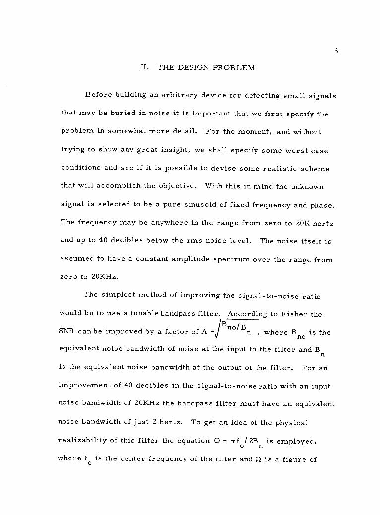
II. THE DESIGN PROBLEM
Before building an arbitrary device for detecting small signals
that may be buried in noise it is important that we first specify the
problem in somewhat more detail. For the moment, and without
trying to show any great insight, we shall specify some worst case
conditions and see if it is possible to devise some realistic scheme
that will accomplish the objective. With this in mind the unknown
signal is selected to be a pure sinusoid of fixed frequency and phase.
The frequency may be anywhere in the range from zero to 20K hertz
and up to 40 decibles below the rms noise level. The noise itself is
assumed to have a constant amplitude spectrum over the range from
zero to 20KHz.
The simplest method of improving the signal-to-noise ratio
would be to use a tunable bandpass filter. According to Fisher the
SNR can be improved by a factor of A =J Bno/Bn , where Bno is the
equivalent noise bandwidth of noise at the input to the filter and Bn
is the equivalent noise bandwidth at the output of the filter. For an
improvement of 40 decibles in the signal-to-noise ratio with an input
noise bandwidth of 20KHz the bandpass filter must have an equivalent
noise bandwidth of just 2 hertz. To get an idea of the physical
realizability of this filter the equation Q = Trfo/ 2Bn is employed,
where fo is the center frequency of the filter and Q is a figure of
1merit often associated with frequency dependent devices. Using
this equation it is seen that to get a two cycle bandwidth at 20KHz
would require a filter Q of 15, 700 which is completely unrealizable.
Furthermore, if the signal frequency drifts by as little as . 1% it
would be severely attenuated.
At this point one recognizes the need for a fresh approach to
the problem. Perhaps one of the more powerful tools that is avail-
able to scientists, such as correlation, can be implemented here.
The correlation equation is shown below.
T/2R(T) = lim J x(t)y(t +T) dt
T--*-00 -T/2(2)
4
In order to apply this to the signal detection problem x(t) is set equal
to the unknown signal plus noise, s(t) + n(t), and y(t) is set equal to
s'(t), a signal which has the same frequency and a constant phase
relationship with respect to s(t). The limit and integration constitute
a time averaging process. The correlation equation can then be
written as
R(T) = [ s(t) + n(t)] s'(t +T ) (3)
'In this case Q = fo/f
2- fl' where f
2and f
1are the upper and
lower half power frequencies (3 db. points).

5
where the bar indicates taking the time average. Multiplying the
right hand side out gives
R(T) = s(t)s'(t +7) + n(t)s'(t +T) (4)
But if the noise is assumed to be completely random and thus non-
coherent with the signal, then n(t) and s'(t +T) are statistically
independent and may be time averaged separately. Since the noise
has a zero mean value, then the last term of equation (4) will be zero.
Then if s'(t +T) is of fixed amplitude and T is taken as zero, the
correlation equation reduces to
R(0) = s(t)s'(t) (5)
which is the desired result. Thus if we can only find some way of
physically implementing the correlation equation then we should be
able to produce a d. c. signal, R(0), that is proportional to the
amplitude of the unknown signal, s(t), but entirely free of noise.
In building the correlator it is seen that equation (2) can be
implemented with not too much difficulty. Taking the product of
x(t) and y(t) is a simple process, and an integrator is easily built
out of a low-pass filter. The problem arises in trying to establish
the integration time. From equation (2) it is seen the ideal integra-
tion time, extends for all time from minus infinity to plus infinity.
To produce this with a low-pass filter would require an infinitly
small bandwidth (infinite time constant), and this is highly impractical.
6
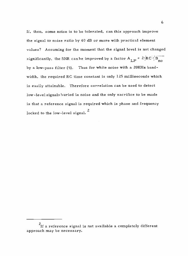
If, then, some noise is to be tolerated, can this approach improve
the signal to noise ratio by 40 dB or more with practical element
values? Assuming for the moment that the signal level is not changed
significantly, the SNR can be improved by a factor Ar- ---= 2,RCLP " no
by a low-pass filter (5). Thus for white noise with a 20KHz band-
width, the required RC time constant is only 125 milliseconds which
is easily attainable. Therefore correlation can be used to detect
low -level signals buried in noise and the only sacrifice to be made
is that a reference signal is required which is phase and frequency
locked to the low-level signal. 2
2If a reference signal is not available a completely differentapproach may be necessary.

7
III. THE LOCK-IN AMPLIFIER
The lock-in amplifier is a device which physically implements
the correlation equation. Several modifications have been made to
simplify in the construction and use of the device. The integration
time (low-pass filter time constant) has been made finite. Also,
since a shift in time has the same effect as a shift in phase for a
sinusoidal signal, the time shift is replaced with a phase shift
network, which is easier to build.
A simplified diagram of the lock-in amplifier is shown in Figure
1. The tuned amplifier is included in the signal input channel to reduce
SIGNAL
INPUTCHANNEL
REFERENCE
INPUTCHANNEL
high gaintunedamplifier
0- phaseshifter
waveshaper
mixer
Figure 1. The lock-in amplifier
low passfilter
0 meter

8
the signal-to-noise ratio to the extent that the signal will receive
adequate gain without having the noise saturate the following circuitry. 3
The exact design of the wave shaper depends on the type of mixer
used, but in general the output of the wave shaper is a constant
amplitude signal, independent of the amplitude of the reference signal
input and with the same frequency.
In choosing the mixer one is faced with the choice of several
possible designs, but the final choice depends on performance and
cost. One possible choice would be a true product mixer or multi-
plier. The multiplier would require a constant amplitude sine wave
from the reference channel and would multiply this by the unknown
signal from the signal input channel. If the two signals are locked
together in frequency the result will be a second harmonic super-
imposed upon a d-c signal. The second harmonic is filtered out by
the low-pass filter so only the d-c portion remains. The amplitude
of the d-c signal is equal to the peak value of the unknown signal
times the peak value of the reference signal times the cosine of the
phase difference between the two signals. Thus when the phase
shifter changes the phase from zero to 180° the output will change
from its positive maximum to its negative maximum. The
3 The peak-to-peak noise voltage is approximately ten timesgreater than the rms value.

9
disadvantage of the true product mixer is that it is often costly and
difficult to build with high reliability. A less costly device would be
the switch type mixer. In this device the reference signal is a
square wave of amplitude ± 1. When this reference is multiplied by
the unknown signal, the result is an output signal that equals the
unknown input for half a cycle and is an inversion of the unknown
signal for the other half of a cycle (the unknown and reference are
still locked together in frequency). If there is no phase shift between
the signal and reference the output will appear to be a full wave
rectification of the input (Figure 2a). Thus the switch type mixer
is also called a synchronous rectifier. The output of the switch
type mixer will appear to be a synchronous rectification of the input
and be independent of the amplitude of the reference square wave.
The maximum value of the d-c signal in the output will be . 637 times
the peak value of the unknown signal input and will again vary as the
cosine of the phase difference between the signal and the reference.
A synchronous rectifier has the advantage that it is less costly and
easier to fabricate than a true multiplier. The disadvantage with
synchronous rectification is the fact that the reference input must
be converted to a square wave and also, since the spectrum for a
square wave contains all the odd harmonics of the fundamental
frequency, noise centered about these harmonics is also shifted
down to zero frequency. But the contributions from the higher
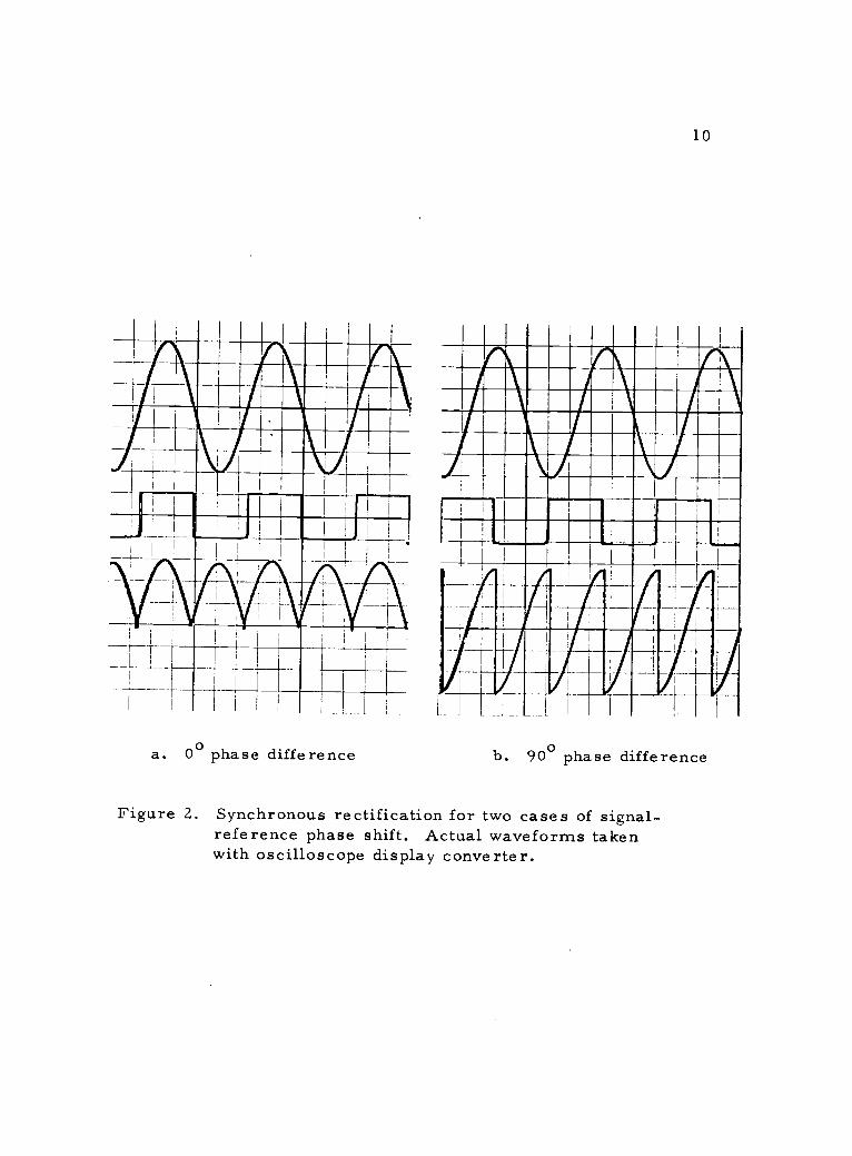
a. 0o phase difference
10
1111111A.NA/1111111Mpumval ir
l
b. 90° phase difference
Figure 2. Synchronous rectification for two cases of signal-reference phase shift. Actual waveforms takenwith oscilloscope display converter.

11
harmonics varies inversely with the order of the harmonic and can
be practically eliminated by increasing the Q of the bandpass filter
in the signal input channel.

12
IV. DESIGN OBJECTIVES
Before examining the circuitry of the lock- in amplifier it may
be helpful to first understand the philosophy behind the designing and
building of the device. The main objective was to build a lock-in am-
plifier capable of detecting very small signal levels in the range of
one to ten nanovolts. Furthermore the device should be capable of
detecting this signal when it is buried up to 60 decibels below the
rms noise level. The desired frequency range was selected to be
100 Hz to 20 KHz. Another objective was to utilize integrated circuit
operational amplifiers whenever possible in building the lock-in am-
plifier. The purpose of this was to determine whether these opera-
tional amplifiers could be successfully used in a multistage device
while still satisfying the necessary requirements such as proper
input and output impedance, bandwidth, and gain.
In designing, building, and testing of the lock-in amplifier the
major emphasis was on satisfying the above objectives. Therefore
much more attention was given to the design performance and in-
creasing the quality of performance than was given to the many minor
details that are associated with a marketable product.

13
V. CIRCUIT DESIGN
For the sake of clarity a detailed block diagram of the entire
system is shown in Figure 3. The design of the signal input channel
will be considered first.
SIGNAL INPUT CHANNEL
(;)-- A=10sig. II
tunablebandpassfilter
REFERENCE INPUT CHANNEL
r
0--Lref.
phaseshifter
A=1.0
MIXER
inverter
synchronousrectifier
amplifier-clipper
waveshaper
LOW PASSj FILTER
Figure 3. Lock-in amplifier block diagram.
Signal Input Channel
The signal input channel consists of two high gain amplifiers,
a bandpass filter, and a unity gain inverter. The requirements of
this channel are well suited for the application of integrated circuit

14
operational amplifiers. The operational amplifier used for this
project was the Fairchild uA709C. The 709C is a general purpose
device which exhibits over 90 decibels of open-loop gain and has a
very large input impedance. These characteristics make it well
suited for use in the traditional operational amplifier configuration
shown in Figure 4. In this configuration the gain can be determined
very accurately and is given by A = Rf/Ri. The capacitors C1, C2,
R.
Rf
Figure 4. Inverting operational amplifier configuration.
and resistor R1 are frequency compensation elements whose functions
are to provide some local feedback to the IC (integrated circuit) to
insure stability. The frequency compensation components along with
the gain of the operational amplifier determine the upper-cutoff
frequency. Since the gain-bandwidth product is a constant, some
bandwidth must be sacrifieced in order to achieve a large gain. For
a particular set of frequency compensation components, reducing

15
the gain by a factor of ten will increase the bandwidth by a factor of
ten. This can be potentially troublesome because by reducing the
gain, the bandwidth could be extended beyond its stable limit, which
is about one megahertz.
One of the requirements of the first stage of the signal input
channel is a large input resistance to prevent loading on the device
being measured. If the operational amplifier is to be used in the
normal configuration shown in Figure 4 then the input resistance
would be equal to R.. For a one megohm input resistance R. would
have to be one megohm and Rf would have to be 1000 megohms for
60 dB of gain. Not only is 1000 megohms impractical for the feed-
back resistor, but the small bias currents flowing in the one megohm
resistor would produce a d-c voltage at the inverting input which would
be amplified to the output, possibly causing it to saturate. To prevent
any unduely large d-c offset voltages at the output, the resistance path
from the inputs to ground should be less than 50K ohms. Further-
more, in order to minimize the noise level at the output, an equiva-
lent input resistance of about one kilohm is optimum.
The amplifier shown in Figure 5 is a non-inverting amplifier
which takes advantage of the large input resistance appearing at the
non-inverting input. According to feedback theory, with resistor
R2 disconnected, the input resistance at the non-inverting input is

16
R31M
Figure 5. Non-inverting amplifier.
given as the open-loop input resistance times the loop gain ( 3 ). 4
Since for the 709C the open-loop input resistance is 250K ohms and
the loop gain for the feedback shown in Figure 5 is about 40, then
the input resistance would be about 10 megohms. But the operational
amplifier won't function without a d-c path to ground for the bias
currents of the IC input transistors. This path is furnished by
resistor R2 which acts as a bootstrapping resistor. Since resistor
R2 (25K ohms) parallels the 250K ohm input resistance, through
capacitor C2, the closed-loop input resistance is reduced by factor
of ten. The bootstrapping thus causes the 25K ohm resistor to
appear larger by a factor equal to the loop gain. Capacitor Cl
is the input coupling capacitor and capacitor C2 is needed to prevent
4 The loop gain is defined as the open-loop gain divided by theclosed-loop gain.
17
a large d-c offset in the output due to the bias current flowing in R2.
The d-c bias current for the inverting input is supplied through the
feedback resistor. Supplying bias through the large feedback resistor
does not produce a noticeable offset voltage because any offset that
may be present is cancelled by the action of the negative feedback.
The lower-cutoff frequency is determined by capacitor C2. Capacitor
Cl sees such a large input impedance that it essentially has no effect
on the frequency response. But capacitor C2 sees a virtual ground
on one side and a one kilohm resistor on the other side. With C2 at
two microfarads the lower-cutoff frequency is fixed at about 80 hertz.
The upper-cutoff frequency is determined by the frequency compen-
sation components and has been adjusted to about 30 KHz minimum.
The complete circuit diagram for the signal input channel is shown
in Figure 8, while the circuit diagram for the complete lock-in
amplifier is shown in Appendix 1. These diagrams show that the
feedback resistors of the two high-gain amplifiers are actually on
switches and can be varied to give gains of 20, 40, or 60 decibels.
The second stage of the signal input channel is a bandpass
filter. The bandpass filter must be tunable so that its center
frequency can be set to any frequency within range of the lock-in
amplifier. Furthermore, it is desirable to change the Q of the filter.
A filter satisfying these requirements is shown in Figure 6. This
filter uses the operational amplifier as a negative impedance converter
18
and by applying the proper passive networks to the input and output,
an active bandpass filter is realized (2). The transfer function for
this filter is given by
H( s) -e( s) oute( s).in
1
-K s R6*IC42 1 1 K 1
s + s'14.6*.C3 + R7*C4 R6*C4/ + R6*C3*R7*C4
(6)
where K is the gain factor of the negative impedance converter. Since
K is a positive constant the minus sign indicates that the filter does
invert the signal.
Figure 6. Bandpass filter.
From the transfer function it can be seen that if R6=P7 and C3=C4
then the parameters such as the center frequency, fo; the gain, Ao;

and the filter Q are given by
1fo
2Tr *R6*C3
A
Q
Ko 2 - K
1
2 - K
19
These equations indicate that the frequency can be tuned by simul-
taneously changing either the two resistors or the two capacitors.
Furthermore, changing the center frequency will not effect either
the gain or the filter Q. The Q is changed by adjusting the potentio-
meter on the output of the operational amplifier, which alters K in
equation (8) and (9). Unfortunately, whenever the filter Q is changed,
the gain at the center frequency also changes. Thus whenever the Q
is changed the signal input channel must be recalibrated so that the
output will give an accurate measure of the signal level at the input.
If R6 doesn't equal R7 exactly or if C3 doesn't equal C4 exactly then
the gain at the center frequency is given by
2 - 1/QA
o (C4/C3 - 1) + (R6/R7 - 1) + 1/Q (10)
From this equation it can be seen that if Q = 10 and C3 = C4, then if
R6 varied from R7 by as much as 10% the gain would be reduced by
50% for R6 > R7, and would be equal to infinity for R6 < R7. In order
to avoid large gains which cause the filter to break into oscillation,
the resistors R6 and R7 must be part of a precision compound

20
potentiometer and capacitors C3 and C4 must have low tolerance.
Actually the gain is more likely to be low than high because R6 is
increased by the output impedance of the previous stage and R7 is
reduced by the shunting effect of the input impedance of the following
stage. In order to reduce the effect of these impedances it is desired
that the output impedance of the previous stage be less than 100 times
the smallest resistance that R6 may have and the input impedance
of the following stage be more than 100 times the largest value that
R7 may have. Since R6 and R7 are designed to vary from 2K to 20K
ohms the output impedance of the previous stage should be less than
20 ohms and the input impedance of the following stage should be
greater than 2 megohms. According to feedback theory (3) the output
impedance of the first stage is equal to the open-loop output imped-
ance (about 200 ohms) divided by the loop gain. This makes the
maximum output impedance about 5 ohms.
The third stage of the signal input channel is shown in Figure
7. It is a high-gain amplifier used in the non-inverting mode to
achieve the maximum input impedance. This stage is very similar
to stage one except for the bootstrapping resistor. This stage is
direct coupled to the previous stage, eliminating the need for the
bootstrap resistor. The input resistance to this stage is equal to
the open loop-input resistance (250K ohms) times the loop gain,
which results in an input impedance of at least 10 megohms. The

21
R10
Figure 7. Third stage high-gain amplifier.
capacitor C5 is included to prevent amplification of the small d-c
offset from the previous stage. The low-frequency cutoff point is
determined by capacitor C5 and resistor R9 in the same manner as
in stage one. The detailed diagram of the signal input channel shown
in Figure 8 shows that the loop gain of the third stage can be varied
to produce gains of 20, 40, and 60 decibels, just as was done in stage
one.
The fourth stage of the signal input channel is a unity-gain
signal inverter. This stage, shown in Figure 8, could be built with
discrete transistors instead of the operational amplifier with a slight
savings in cost. The advantages of the operational amplifier in this
application are its wide dynamic range (± 14 volts at the output) and
its ease of adjusting the gain. As will be shown later the wide
dynamic range is not necessarily needed here because the next stage,
the mixer, has a rather limited dynamic range. The operational

Input
1K
Figure 8. Complete signal input channel.

23
amplifier does have the additional advantages of being compact
and requiring only a minimum of additional components.
Reference Input Channel
The reference input channel has two main functions. The first
is to provide an adjustable phase shift of a sinusoidal signal for a
range of at least 180 degrees. The other function is to supply a
constant amplitude square wave to the mixer. The frequency of the
square wave must be the same as the frequency of the signal applied
to the reference input. The input impedance at the reference input
is not critical but should not load down the signal source. The signal
level at the source is not critical either, as long as it is within the
proper range. The reference channel is designed to work properly
for a signal as small as one millivolt and as large as one volt peak-
to-peak. With an attenuator in front of the channel the maximum
signal level can be extended for larger values.
The first stage of the reference input channel is the phase
shifter, as shown in Figure 9. The heart of the phase shifter is the
capacitor and variable resistor combination connected between the
collector and emitter of the first two transistors. This combination
forms a phase divider network. By driving the two ends of the phase
divider with signals 180 degrees out of phase (emitter and collector)

24
Figure 9. Phase shifter.
the output of the phase divider is equal to the signal at the emitter
input, but with a phase shift given by
-1 12 tan RCf
where C is the capacitor of the phase divider, R is the equivalent
resistance that the capacitor sees, and f is the input frequency. In
Figure 9 there are two phase divider networks to insure that a phase
shift of over 180 degrees is possible. According to equation (11),
180 degrees of phase shift is possible with one phase divider, only
if R can vary between zero and infinity which is not possible. The
switch on the output of the third transistor provides a discrete phase
change of 180 degrees. The capacitors in each of the phase divider
el

25
networks are changed in decade increments with a frequency range
switch which also changes the tuning capacitors in the bandpass
filter of the signal input channel.
The stage following the phase shifter is a combination amplifier
and clipper. The circuit diagram for this stage is shown in Figure
10. The two diodes in the feedback loop are high speed silicon diodes.
Figure 10. Amplifier-clipper.
Since the diodes have a high resistance for voltages less than the cutin
voltage of the diode, the gain of the operational amplifier will be
large until the output voltage reaches this level. When the output
voltage exceeds the cutin voltage one of the diodes will be forward
biased, reducing its resistance and decreasing the gain. Thus a
sine wave input will be amplified at the output, but the positive and
negative peaks will be clipped off. Because of the clipping action of
the diodes this circuit can be driven by a high level signal without
saturating and still provide adequate gain for low level signals. The
maximum signal level is actually limited by the previous stage

26
(phase shifter) which produces some distortion for signal levels
greater than one volt rms.
The final stage of the reference input channel is the wave
shaper . The function of this stage is to convert the signal coming
from the amplifier-clipper to a signal which will drive the mixer.
The mixer requires two square waves, 180 degrees out of phase,
Figure 11. Wave Shaper.
whose amplitude varies between . 5 volt and 5 volts. The circuit
selected to do this is the Schmitt trigger shown in Figure 11. The
circuit is in the standard Schmitt trigger configuration except for
two modifications. The resistive divider network composed of
resistors R36, R37, and R38 are included to reduce hysteresis.

27
Hysteresis is undesirable because it causes the output square wave
to be unsymmetrical and, furthermore, it limits the minimum signal
amplitude the reference signal can have. It is undesirable to
completely eliminate the hysteresis because in doing this the rise
time of the square wave is also reduced, which in turn lowers the
frequency response. The Schmidt trigger of Figure 11 is designed
to operate over a frequency range of 40 hertz to 30 KHz, with the
hysteresis reduced from about two volts to ten millivolts with the
divider network. The second modification of the Schmitt trigger is
the divider network on the input, composed of resistors R26, R27,
R28, and R29, along with the input coupling capacitor. This
combination of resistors and capacitor allows the d-c level at the
input to be adjusted so that transistor T4 is biased midway between
the upper triggering level and the lower triggering level. This tends
to counter the unsymmetrical effect of hysteresis on the output
square wave.
Mixer and Low-Pass Filter
It is the function of the mixer to provide synchronous rectifica-
tion of the output of the signal input channel. This can be done with-
out much complexity using junction field effect transistors in the
configuration shown in Figure 12. This type of mixer requires
complementary inputs (180° degrees out of phase) from both the

28
signal input channel (SIG 1 and SIG 2) and the reference input channel
(REF1 and REF 2), and also provides a pair of complementary
outputs for the following stage. The junction field effect transistors
(J-FET's) act like series switches. When the reference signal level
is at . 5 volts the source to drain resistance of the J-FET is about
250 ohms. When the reference level changes to 5 volts the source
to drain resistance becomes very large. If the input resistance of
the following stage is about 12K ohms then only about 2% of the signal
will fall across the J-FET when the reference level is low, with 98%
appearing at the respective output. When the reference is high over
99. 9% of the signal falls across the J-FET, meaning it is essentially
an open circuit. Capacitors C11 and C12 are required to prevent the
d-c offset voltages of the previous stages from getting to the low-pass
filter. Resistor R39 and R40 supply the d-c path to ground for the
bias currents of the operational amplifier in the following stage.
C11
Sig 1 0
Sig 2
R39 Ref2
0 + OUT
o OUT
R40
C12
Ref1
Figure 12. J-FET switch type mixer.

29
The only difficulty with this type of mixer is that it has a
rather limited dynamic range. If the signal level at the drain of the
J-FET exceeds one volt peak-to-peak then the gate-drain junction is
in danger of being forward biased, which could direct couple the
Schmitt trigger with the low-pass filter. Also the drain to source
resistance of the J-FET is not independent of the input signal level.
In making measurements where the noise level is much higher than the
signal level, some of the negative peak excursions are attenuated more
than the positive peak excursions by the nonlinear action of an "on"
J-FZT. This will cause the d-c level of the noise to shift producing
an offset at the output of the low-pass filter. Since this offset has the
same polarity at both the + and - outputs, it is partially eliminated
by the common mode rejection of the differential low-pass filter.
But it is not eliminated completely and still shows up at the output
when the noise level into the mixer exceeds 500 millivolts peak-to-
peak.
The final stage of the lock-in amplifier is the low-pass filter.
The function of the low-pass filter is to convert the signal at the
output of the mixer to a stable d-c voltage that can be measured with
a meter. The circuit designed to achieve this is shown in Figure 13.
This curcuit is basically in the form of an operational amplifier
integrator (3). The resistor in the feedback loop, R45, is actually
an important variation from the typical integrator configuration. Its

30
C15
Figure 13. Low-pass filter.
purpose is to provide some negative feedback for the d-c signal,
stabilizing the output and reducing long term voltage drifts. Another
variation is the fact that the integrator has a double-ended input.
If R45 is much greater than R41 + R42 then the gain is nearly the
same at each input and the output is twice as large as the same
integrator would have with a single-ended input. The d-c gain from
the negative input to output is given by R45/(R41+R4 2). The time
constant for this filter is simply equal to the product of capacitor
C15 and resistor R45. The equivalent noise bandwidth of the lock-in
amplifier is related to the time constant of the low-pass filter and
is given by
EQUIVALENT NOISE BANDWIDTH 4RC1
(12)
31
where R is equal to R45 and C is equal to C15. Therefore the
equivalent noise bandwidth of the lock-in amplifier can be easily
adjusted by changing capacitor C15. Capacitors C13 and C14,
although large, don't have much effect on the equivalent noise band-
width except when C15 is very small (on the order of . 1 ufarad).
The purpose of these capacitors is to present an equal input impedance
at each input to the large noise excursions from the mixer. This
helps in reducing the offset caused by the nonlinear action of the
mixer on large noise levels. The meter is a d-c microammeter
which reads center zero and 100 microamp full scale in either direct-
ion. Resistor R46 is adjusted so that the meter is reading directly
proportional to the rms voltage level of the input signal. The constant
of proportionality is determined by the reciprocal of the total gain of
the signal input channel.

32
VI.' SYSTEM PERFORMANCE
In order to demonstrate the performance of the lock-in amplifier
graphically a X-Y plotter was connected to the output of the LIA (lock-
in amplifier). The X-Y plotter contains a calibrated sweep generator
that allows the d-c output of the lock-in amplifier to be plotted against
time. The equipment set-up for determining the system performance
is shown in Figure 14. The variable precision attenuator is a com-
pletely shielded device capable of providing up to 100 dB of attenua-
tion in 1 or 10 dB steps. The TEST LIA refers to the lock-in ampli-
fier described on the preceeding pages of this thesis, while the PAR
LIA refers to the Princeton Applied Research lock-in amplifier that
was used here for a performance comparison.
signalgenerator
noisegen.
variableprecision
attenuator
PAR LIA
TEST LIA
Figure 14. System test set-up.
X-Y
plotter

33
In rating the performance of the lock-in amplifier the features
to be analyzed are its frequency response, the minimum signal -to-
noise ratio that can be tolerated, and the minimum signal level that
can be accurately measured. The minimum signal level that can be
accurately measured is rather difficult to determine since there is
nothing to compare the results with in this range. The smallest
sensitivity range of the PAR lock-in amplifier is 10 µ V. The
minimum signal level the PAR can measure with less than 10% error
is 111 V. The test lock-in amplifier is designed to measure signals
in the nanovolt range which is below the accurate range of the PAR
unit. The proceedure used in measuring these small signals is first
to calibrate the test unit using the PAR lock-in amplifier and a
10 µ V input signal. The attenuation to the input signal is then
increased in 20 dB steps while the gain of the signal input channel
of the test LLA. is also increased in 20 dB steps. If the output of the
lock-in amplifier continues to give a full scale deflection then this
is a good indication that the lock-in amplifier is reading the correct
value.
The principle source of error in measureing low-level signals
is caused by coupling of the signal from the reference channel into
the signal channel. In order to determine the effect of this coupling,
the low-level input signal is shorted out at the attenuator. Since the
reference signal is uneffected by this, any coupling of the reference
34
signal into the signal input channel should show an offset at the
output (input still shorted out).
Another indication of the performance of the lock-in amplifier
is the symmetry of the output when the phase of the reference signal
is changed by 180 degrees. If the output is offset when the input is
shorted the symmetry should still exist either about the offset level
or the true zero level depending on the origin of the contaminating
signal. Thus we have several indicators as to the accuracy of the
lock-in amplifier when it performs as expected.
At the limit of its sensitivity the lock-in amplifier will no
longer perform as expected. The output may be above or below the
expected value or the symmetry of the output may be badly skewed,
In this case since it isn't known if the error is caused by the attenu-
ator or the lock-in amplifier, the amplitude of the input signal can
no longer be determined with any certainty.
The output results are shown in Figures 15 through 20. On
each graph are three black triangles which mark the instants when
the input was grounded, when the reference phase was changed by
180 degrees, and when the input was ungrounded. On each graph
is also listed the operating frequency, the approximate signal-to-
noise ratio (SNR), and the filter time constant of the lock-in ampli-
fier. The first three figures show a comparison of the test unit and
the PAR unit over the frequency range of the test lock-in amplifier.

35
The test unit seems to perform satisfactorily over this range while
the PAR unit shows some variation when the phase is changed (input
grounded). It is especially noticable at the higher frequencies indi-
cating that in this range a greater portion of the reference signal is
coupled into the signal channel. Figure 18 demonstrates the opera-
tion of the test unit when the signal level is reduced 40 dB below the
10p. V level that was used to calibrate the device. The two graphs
in Figure 19 were taken with the input signal reduced 60 dB below
the l0µ V level. These graphs show a variation from the expected
value (10 nV) and enough distortion to place some question as to
what the signal level actually is. The two graphs of Figure 20 were
taken with a random noise generator connected to the input (see
Figure 14). The signal level for these graphs was set to 10 p. V and
then the noise level was increased first to 1 mV (SNR = 40 dB) and
then to 3. 16 m V (SNR = 50 dB),

36
1
.5
-. 5
-1
.... ......._...,...,_ ......:mgErsimmunsrawartunipan.mattg:NEmEnepunTiii,ffi:kinans Iminsal
_El,,:ararr
1-'.-utcuimemer.a.ar-...........
PAR LIA.;-,
+-L-1:
mn..7-t-s.. ! --,
4_
'-;-. IlEirm
I- Lim. I= + + -f-+ t f-
miline t.,--
11 '-' MIMEto+Insu;:ms4r .-+-t-t.-
+----t+-r -'71-, 99mu.... EEE: inEsiB==wins
Emu:NE 01 m. Ins MIIIINWMN.
MOMIIIM
NM3 '' g Emuraj mEINE.MEM rf = 2 kHz MSSEmximorteIN SNR = -18 dB
filter TC = 1. secr ME -+----
.
! ! , ! ,--, ! !--i-4-4- rn+ 4--q
f
ft+ ,
t-4.....ME , Mliil4
0
1
.5
> 0
.5
-1
20 40
SECONDS
60 80
--f--"t f-fr,*T....
4.-__ .-...' -.. -t-+- .-,44-1- ---,-,-i- --,-4-1---,- .
, u_ TEST LIA --,-,--.
H-' 11 --.-.--t- ,-'' '-!- , ,_ttr
NMIL__ - i- '-r-,,-,--1-- .
- y-I- ,--1-*
-- ---4-,-;
,- --.--, --1-.--4.- -,--,-'-'r
V,---T-r ,,
4-,,
1:trI-
f = 2 kHz -1= '-_4
SNR = -18 dB 11.,_h...
filter TC = 1 sec.
..± ..___ _mumMOW
--1-*--
_,_
-'-' .._,___ '-,-..--t.-1.rr-
--"-t-'',
- -an
'-'-'-r. ___, ... - '.-. .- ,-
- r
20 40
SECONDS
60 80
Figure 15. Intermediate frequency comparison of the PARlock-in amplifier with the test lock-in amplifierfor a 1 uV input signal.

1
.5
0
s
1
0
1
.5
0
em 'e pie P1712:afffIFIIIIInos _,--_, . mums isLL 9 PAR LIA
T.. 74 74-44_
sus=3 us ...jaw .nr In_rr
1--- tfti:t .1 At_L,_
#±1--,
arm irirgintomr '-r- 4,44
,--r -f--i--,
-'47-.4.,--i-14-
ti'- 16lhgalln±-Ttt 1-4 r4L-rEl 4,-
.
---, --
InIngraimum,: -, L F-H 4-- slamreritill mulaVIERN
4---_IV...49Ers.
-,--,-...11--i
.iEr,.....d..:Biin
N,_,_,_,.:r E. In
1M i f tauspaaB. f = 30 kHz. . SNR = -18 dBeonImo filter TC = .1 sec .11 Ir. -r.
tr--'
-rff.--T---- H.--,--,-,-- --
_
Ea'--t Ej--`,1 Tri 12ftr, --h-iWS ,
ri--- I-- ---,
20SECONDS
60
.I.......on II:----iiEratzvainFin
...110-.".....02 ,L LiaTES T t,_
--t-tt- IN
- ,
,
_ .- '4___.,
,LIA
_,_,_4_4. ,.
+- t
if" l -4-
4-ti-t Er:-1-1!4
' t -f-
Nou Ns r _
Ti1--,--E _ , -..-` 4- -=-L
_J
4_44_,,_,_-44_, 4__:.
__,t,_,.-,-,,-:-,_ - --.
H--
r,,z4 '-t- :1'1 _I-i ,- 22 r-t,2t'- '-' ---t 1M
'-',-,-,_-, r
f = 30 kHzSNR = -18 dBfilter
nil- - :7- _.
---,4TC = .1 sec
0 20 40SECONDS
60
37
Figure 16. High frequency comparison of the PAR LIA.and the TEST LIA. with a 1 uV input signal.

38
1
.5
> 0
- 5
-1
1
.5
0
-. 5
0
1-t=t, -4- ! -1- i-,-,
- ,__, 1- ' PAR LIAM'.2iLT0-
r. _
0T-1-4-
r,m
?may
MEEr t Mi MEENI
MI. A
'-1
-H E r---t-t- L
. Anni . -
1---
f
P-
-2-Ttt -
190
11-1:4-
MHz
-V--'
7-7ft±
ewe
L,
4-1 4,-M-,,
=
,KEEN MaliENE ME
SNR = -18 co winillfilter TC = 1 sec
-1 4-1- 1- .-T ' ,,......"-LEINEM-1---,-r ,14._ ft .a.EgowassEnv 020
SECONDS40 60
.11
7
111 1---- MITEIREME--W -47 TEST LIA Eltemr*
, 7 MEE-
--,
'--
.--,f = 190 HzSNR = -18 dBfilter TC = . 5 sec
--,-,
r 1
_
20 40
SECONDS
60
Figure 17. Low frequency comparison of the PAR LIAand the TEST LIA for a 1 uV input signal.

100
50
-1
39
,,fm.,.......H-t-
-i_--c -
,..............
TEST LIA
. _,,.....,..,
:rd.. ...a._,LF4. .........n
Oa ,_i 1
....,i_fi
-1-,,_ 4_+---t -r
,- .,_,..,. '---,'.- . t , 4..,_t ,- ---__,, .... -7--,-
4_,_.
-1
-1-t-`--
_:_--- rt KMir-Es
-
4_,
ENr-'-'
-r__T-.,_
L.,7
egg,H-1-
,-----r4-'---_L,__tr_
4-r-
,_ t
Es
. 1. .LI r
is _14
'77'-' --,t+
-H-;--
man
....
,-, , '41
ige4+1-
--H.-,-
r,. f = 2 IcHzSNR = -38 a .,_
_ _, ---c
_..., I_
'-ITA----4_
,--_,-filter TC = 4 sec
,_- -
Inn0 50
SECONDS
tTit
0
t_tf
- 50
f = 190 HzSNR = -38 dB
-100 filter TC = 1 sec
0 20 40 60 80
SECONDS
Figure 18. Output data of the test lock-in amplifier at inter-mediate and low frequency for a 100 nV inputsignal.

10
5
5
-10
10
0
-10
40
._,_
--4-I--L_i_-r - _.
_i_L-i- r-r. '` ' I .
4.
- ,
-t-r- -r- .-
r-t---r-,--,--r , ----, - i- r-,---
TEST LIA t -
-r-'-r-
I-
1-
- I
r--H
I,-- - - - -i -,-
, FL'ti.I-I-H ---H-f 7-- -.-
4-4 -++ r
_ --1--
T
1,-1-7--,--H-,-- Irr - RENE...-,,__,
'-7 1lig+,,,-_-,-,
_TT__
''
___'--,17/-I
, _4=4_' t
-ff-Inti---
,
aTH 4H--,-.' ,
it rtf
I- J-1-,-i-
, -r-
'' ITHtli --'1HIS 11'-''- EREPIMNIIMME NB:11M il-ht:EU 1T-1111t- EiMr
NNWUM
EMMEN= we magprd pj_i_'
!
IBMi La
,-H.,-f = 2 kHza
4-rIBM
1-- ,4 , _i_j,_ 1 HSNR = -58 dB aM , ,___t E. , -r-Mil
hi--, --,- -,--
--__filter TC = 8 sec t. --f---H4L: ill _.,..._ . .
ti_,-i- 1. 4
-_._ n-
-11al t-1=
_,.----h- '±--' 4----
4 '-I----" -t- T'llt -r M 4-,-- '-'- all alErlra ft
,
Eralmuniza.......E40 50 100
SECONDS
150 200 250
tt
TEST LIA_
--,
--r
---
_
- ,-.
r-r - -r-.--,-..Nu - _ _..
- --,
-::r r__
r' :77
.. __ .,_
--r-.._ .
f = 2 kHz _..,.__
SNR = -58 dB,
...
_filter TC = 12 secEr
1Mr
-50 100 150
SECONDS
200 250
Figure 19. Output data of the test lock-in amplifier at intermediatefrequency for a 10 nV input signal.

10
> 0
-5
-10
ram- rimmttimain. ri... immai,,.
4'4 _i_l_}
TEST LIA -.-h"--', 7 ,
]-4.- r Ma --i-I. IMI
1
E--r- '-----r- IMMO
-,INI
MINUM=
omeffoowmilEffl
,._,. T NE ,
IN ---4-!-
II 441--
,-4-
IRE - T i-1-
,}i, 4 rr El
MN......fflISIIIM "'
71 WAMIME-'-÷H-f= 2 kHzSNR = -40 dBfilter TC = 12 sec
1-,- r tr_
.-......,
-t, , APa ---4t
4-:-,-
1 t-_,1i- ----,-,- "t-T- 7 '7- i 1- I
1-1:1-41;0
10
5
0
-5
-10
100 200
SECONDS
300 400
- 1-
1-4- 4 -. -
r 4-1-+ J.-1.-- -""
4-- ---- -1--- --1---,--....._;.-- 1-1
-1-1---,.-- ,--.1-r--1--
4--
-L-1.1 -L.
i'+-147 ' 7 _
TEST LIA-,"
----i
-EN41,
-----r- - . _. --1---,-,-.-.- --.-- -i-,--1.
, ,----1-_,---_,-
- --___,-+-J,-
BE
,41 ii '- J., 1
1-, 41.-t4 - - ---,-'-1-,-.-31is 7_ L': 1 _, ' '-'".4r r 4 '7 -4 MI :-.-
_,_1..4
,--T NM IT-4 `-- Eul_L_.
4.-1. -4.---...-
IEEEf
---.-
= 2 kHzSNR = dB
1-,--50
4----- -4-4--,- ---4
tl-filter TC = 30 sec - -
100 200
SECONDS
300
41
Figure 20. Output data of test lock-in amplifier for signal-to-noise ratios of -40 dB and -50 dB.
42
VII. CONCLUSION
The object of this study was to build a lock-in amplifier capable
of detecting weak signals buried in noise. The ability of the test
lock-in amplifier to detect signals down to 10 nV and to measure
signals down to 100 nV has been successfully demonstrated. The
desired frequency response has also been demonstrated. Another
objective was to utilize integrated circuits in the design and building
of the device. From the circuit design theory it was shown that in-
tegrated circuit operational amplifiers are quite versatile and very
well suited for applications in multistage devices such as the lock-in
amplifier. Thus it has been shown that it is possible to build a
lock-in amplifier utilizing linear integrated circuits that is capable
of detecting very low-level signals that are buried in noise.
43
BIBLIOGRAPHY
1. Brower Laboratories, Incorporated. A practical guide tomeasurement of weak signals buried in noise. Westboro,Massachusetts, 1968. 30 p.
2. Burr-Brown Research Corporation. Handbook of operationalamplifier active RC networks. Tucson, Arizona, 1966. 104 p.
3. Burr-Brown Research Corporation. Handbook of operationalamplifier applications. Tucson, Arizona, 1963. 87 p.
4. Eimbinder, Jerry (ed.). Linear integrated circuits: Theoryand applications. New York, Wiley, 1968. 318 p.
5. Fisher, John C. Lock in the devil, educe him, or take him forthe last ride in a boxcar? Tek Talk 6(1):1-45.
6. Lathi, B. P. An introduction to random signals and communica-tion theory. Scranton, Pennsylvania, International Textbook,1968. 488 p.
7. Moore, Robert D. Lock-in amplifiers for signals buried innoise. Electronics, June 8, 1962, p. 65-68.

APPENDICES

INPUT 1 pf °-1(
22
APPENDIX I
CIRCUIT SCHEMATIC: SIGNAL INPUT CHANNEL, MIXER, LOW -PASS FILTER
20K
1M
10K
10K
. 01 pf 1M
1K 99K
9K
2 pf 2 pf
20K .
01 pf REF 1
REF 2
OUTPUT 0
20K
1 pf
--NA/NA-- 800K
5.6K 5, 6K 4k/NA/-IP---VVV1/4----'
5.6K J 5.6K
25 pf_i_ 251-Lf
FET: 2N4360

47K
33K
CIRCUIT SCHEMATIC: REFTPENCE INPUT CHANNEL
1.5K 1.5K 1. 5K
.010' 01pf
- 50K
1.5K 1.5K 1. 5K
1K
TRANSISTORS
PNP 2N3638 NPN 2N1304

COMPONENT
46
APPENDIX II
Estimated Parts Cost
APPROXIMATEQUANTITY COST
Operational Amplifier 6 $12. 00
Transistor 5 2.00
FET 4 4.00
Diode 2 1.00
Resistor 50 2.00
Potentiometer 4 10.00
Capacitor 40 6. 00
Switch 4 5.00
Misc.* 35.00
TOTAL $77. 00
*Included in the miscellaneous cost estimate are serveral
items that were not included in the test lock-in amplifier but would
be necessary for a complete device. These items include the ± 15
volt power supplies and an internal oscillator that would be capable
of supplying a calibrating signal. Also included in miscellaneous
are items such as the meter, wiring, and the chassis.