re46c190 data sheet - microchip technologyww1.microchip.com/downloads/en/devicedoc/22271a.pdf ·...
TRANSCRIPT

RE46C190CMOS Low Voltage Photoelectric Smoke Detector ASIC
with Interconnect and Timer Mode
Features
• Two AA Battery Operation
• Internal Power On Reset
• Low Quiescent Current Consumption
• Available in 16L N SOIC
• Local Alarm Memory
• Interconnect up to 40 Detectors
• 9 Minute Timer for Sensitivity Control
• Temporal or Continuous Horn Pattern
• Internal Low Battery and Chamber Test
• All Internal Oscillator
• Internal Infrared Emitter Diode (IRED) driver
• Adjustable IRED Drive current
• Adjustable Hush Sensitivity
• 2% Low Battery Set Point
Description
The RE46C190 is a low power, low voltage CMOSphotoelectric type smoke detector IC. With minimalexternal components, this circuit will provide all therequired features for a photoelectric-type smokedetector.
The design incorporates a gain-selectable photoamplifier for use with an infrared emitter/detector pair.
An internal oscillator strobes power to the smokedetection circuitry every 10 seconds, to keep thestandby current to a minimum. If smoke is sensed, thedetection rate is increased to verify an Alarm condition.A high gain mode is available for push button chambertesting.
A check for a low battery condition is performed every86 seconds, and chamber integrity is tested once every43 seconds, when in Standby. The temporal horn pat-tern supports the NFPA 72 emergency evacuation sig-nal.
An interconnect pin allows multiple detectors to beconnected such that, when one unit alarms, all units willsound.
An internal 9 minute timer can be used for a ReducedSensitivity mode.
Utilizing low power CMOS technology, the RE46C190was designed for use in smoke detectors that complywith Underwriters Laboratory Specification UL217 andUL268.
PIN CONFIGURATION
RE46C190 SOIC
VSS 1
2
3
4
5
6
7
8
16
15
14
13
12
11
10
9
IRED
VDD
TEST
TEST2
IRP
IRN
RLED
LX
VBST
HS
HB
IO
IRCAP
FEED
GLED
2010 Microchip Technology Inc. DS22271A-page 1

RE46C190
TYPICAL BLOCK DIAGRAM
Control Logic and
Timing
Trimmed Oscilator
POR and BIAS
+-
+-
VDD (3)
IRCAP (11)
IRN (7)
IRED (2)
TEST (4)
R4
R3
LX (16)
FEED (10)
HS (14)
VBST (15)
RLED (8)
GLED (9)
HB (13)
IRP (6)
VSS (1)
Interconnect
+-
Programmable IRED Current
Programmable Limits
Photo Integrator
Precision Reference
+-
TEST2 (5)
Horn Driver
Level Shift
IO (12)
Current Sense
Boost Control
Boost Comparator
Low Battery Comparator
Smoke Comparator
Programming Control
HighNormal
Hysteresis
DS22271A-page 2 2010 Microchip Technology Inc.

RE46C190
TYPICAL BATTERY APPLICATION
Note 1: C2 should be located as close as possible to the device power pins, and C1 should be located as closeas possible to VSS.
2: R3, R4 and C5 are typical values and may be adjusted to maximize sound pressure.
3: DC-DC converter in High Boost mode (nominal VBST = 9.6V) can draw current pulses of greater than 1A,and is therefore very sensitive to series resistance. Critical components of this resistance are theinductor DC resistance, the internal resistance of the battery and the resistance in the connections fromthe inductor to the battery, from the inductor to the LX pin and from the VSS pin to the battery. In order tofunction properly under full load at VDD= 2V, the total of the inductor and interconnect resistances shouldnot exceed 0.3 . The internal battery resistance should be no more than 0.5 and a low ESR capacitorof 10 µF or more should be connected in parallel with the battery, to average the current draw over theboost converter cycle.
4: Schottky diode D1 must have a maximum peak current rating of at least 1.5A. For best results it shouldhave forward voltage specification of less than 0.5V at 1A, and low reverse leakage.
5: Inductor L1 must have a maximum peak current rating of at least 1.5A.
16
15
14
13
12
11
10
98
7
6
5
3
2
1 VSS
IRED
VDD
TEST
TEST2
IRP
IRN
RLED
FEED
GLED
IRCAP
IO
HB
HS
VBST
LX
RE46C190
D2
D3
4
9
D1
4.7 µFC4
200KR3
1.5MR4
1 nFC5
L110 µH
330
R5
33 µF
C6
To other Units
1 µFC2
100
R1
10 µFC1
VDD
Push-to-Test/Hush
VBST
330
R6100R7
D4
RED
D5
GREEN
C3
Smoke Chamber
Battery
3V
TP1 TP2
VBST
100 µF
2010 Microchip Technology Inc. DS22271A-page 3

RE46C190
NOTES:
DS22271A-page 4 2010 Microchip Technology Inc.

RE46C190
1.0 ELECTRICAL CHARACTERISTICS
Absolute Maximum Ratings†
Supply Voltage .....................................VDD=5.5V; VBST =13V
Input Voltage Range Except FEED, TEST..... VIN = -.3V to VDD +.3V
FEED Input Voltage Range ..................... VINFD =-10 to +22V
TEST Input Voltage Range ......... VINTEST =-.3V to VBST+.3V
Input Current except FEED................................... IIN = 10 mA
Continuous Operating Current (HS, HB, VBST)...... IO= 40 mA
Continuous Operating Current (IRED) ...............IOIR= 300 mA
Operating Temperature ...............................TA = -10 to +60°C
Storage Temperature ............................TSTG = -55 to +125°C
ESD Human Body Model .................................. VHBM = 750V
ESD Machine Model .............................................VMM = 75V
† Notice: Stresses above those listed under “Maximumratings” may cause permanent damage to the device. This isa stress rating only and functional operation of the device atthese or any other conditions above those indicated in theoperation listings of this specification is not implied. Exposureto maximum rating conditions for extended periods may affectdevice reliability.
DC ELECTRICAL CHARACTERISTICSDC Electrical Characteristics: Unless otherwise indicated, all parameters apply at TA = -10 to +60°C, VDD = 3V, VBST = 4.2V, Typical Application (unless otherwise noted)(Note 1, Note 2, Note 3)
Parameter SymbolTest Pin
Min Typ Max Units Conditions
Supply Voltage VDD 3 2 — 5.0 V Operating
Supply Current IDD1 3 — 1 2 µA Standby, Inputs low, No loads, Boost Off, No smoke check
Standby Boost Current
IBST1 15 — 100 — nA Standby, Inputs low, No loads, Boost Off, No smoke check
IRCAP Supply Current
IIRCAP 11 — 500 — µA During smoke check
Boost Voltage VBST1 15 3.0 3.6 4.2 V IRCAP charging for Smoke Check, GLED operationIOUT = 40 mA
VBST2 15 8.5 9.6 10.7 V No local alarm, RLED Operation, IOUT = 40 mA, IO as an input
Input Leakage IINOP 6 -200 — 200 pA IRP = VDD or VSS
7 -200 — 200 pA IRN = VDD or VSS
IIHF 10 — 20 50 µA FEED = 22V; VBST = 9V
IILF 10 -50 -15 — µA FEED = -10V; VBST = 10.7V
Input Voltage Low VIL1 10 — — 2.7 V FEED, VBST = 9V
VIL2 12 — — 800 mV No local alarm, IO as an input
Note 1: Wherever a specific VBST value is listed under test conditions, the VBST is forced externally with the inductor disconnected and the DC-DC converter NOT running.
2: Typical values are for design information only.3: Limits over the specified temperature range are not production tested and are based on characterization
data. Unless otherwise stated, production test is at room temperature with guardbanded limits.4: Not production tested.
2010 Microchip Technology Inc. DS22271A-page 5

RE46C190
Input Voltage High VIH1 10 6.2 — — V FEED; VBST = 9V
VIH2 12 2.0 — — V No local alarm, IO as an input
IO Hysteresis VHYST1 12 — 150 — mV
Input Pull Down Current
IPD1 4, 5 0.25 — 10 µA VIN = VDD
IPDIO1 12 20 — 80 µA VIN = VDD
IPDIO2 12 — — 140 µA VIN = 15V
Output Voltage Low VOL1 13, 14 — — 1 V IOL = 16 mA, VBST = 9V
VOL2 8 — — 300 mV IOL = 10 mA, VBST = 9V
VOL3 9 — — 300 mV IOL = 10 mA, VBST = 3.6V
Output High Voltage VOH1 13, 14 8.5 — — V IOL = 16 mA, VBST = 9V
Output Current IIOH1 12 -4 -5 — mA Alarm, VIO = 3V or VIO = 0V, VBST = 9V
IIODMP 12 5 30 — mA At Conclusion of Local Alarm or Test, VIO=1V
IIRED50 2 45 50 55 mA IRED on, VIRED = 1V, VBST = 5V, IRCAP = 5V, (50 mA option selected; TA = 27°C)
IIRED100 2 90 100 110 mA IRED on, VIRED = 1V, VBST = 5V, IRCAP = 5V, (100 mA option selected; TA = 27°C)
IIRED150 2 135 150 165 mA IRED on, VIRED = 1V, VBST = 5V, IRCAP = 5V, (150 mA option selected; TA = 27°C)
IIRED2050 2 180 200 220 mA IRED on, VIRED = 1V, VBST = 5V, IRCAP = 5V, (200 mA option selected; TA = 27°C)
IRED Current Temperature Coefficient
TCIRED — 0.5 — %/°C VBST = 5V, IRCAP = 5V;Note 4
DC ELECTRICAL CHARACTERISTICS (CONTINUED)DC Electrical Characteristics: Unless otherwise indicated, all parameters apply at TA = -10 to +60°C, VDD = 3V, VBST = 4.2V, Typical Application (unless otherwise noted)(Note 1, Note 2, Note 3)
Parameter SymbolTest Pin
Min Typ Max Units Conditions
Note 1: Wherever a specific VBST value is listed under test conditions, the VBST is forced externally with the inductor disconnected and the DC-DC converter NOT running.
2: Typical values are for design information only.3: Limits over the specified temperature range are not production tested and are based on characterization
data. Unless otherwise stated, production test is at room temperature with guardbanded limits.4: Not production tested.
DS22271A-page 6 2010 Microchip Technology Inc.

RE46C190
Low Battery Alarm Voltage
VLB1 3 2.05 2.1 2.15 V Falling Edge; 2.1V nominal selected
VLB2 3 2.15 2.2 2.25 V Falling Edge; 2.2V nominal selected
VLB3 3 2.25 2.3 2.35 V Falling Edge; 2.3V nominal selected
VLB4 3 2.35 2.4 2.45 V Falling Edge; 2.4V nominal selected
VLB5 3 2.45 2.5 2.55 V Falling Edge; 2.5V nominal selected
VLB6 3 2.55 2.6 2.65 V Falling Edge; 2.6V nominal selected
VLB7 3 2.65 2.7 2.75 V Falling Edge; 2.7V nominal selected
VLB8 3 2.75 2.8 2.85 V Falling Edge; 2.8V nominal selected
Low Battery Hysteresis
VLBHYST 3 — 100 — mV
IRCAP Turn On Voltage
VTIR1 11 3.6 4.0 4.4 V Falling edge; VBST = 5V; IOUT = 20 mA
IRCAP Turn Off Voltage
VTIR2 11 4.0 4.4 4.8 V Rising edge; VBST = 5V; IOUT = 20 mA
DC ELECTRICAL CHARACTERISTICS (CONTINUED)DC Electrical Characteristics: Unless otherwise indicated, all parameters apply at TA = -10 to +60°C, VDD = 3V, VBST = 4.2V, Typical Application (unless otherwise noted)(Note 1, Note 2, Note 3)
Parameter SymbolTest Pin
Min Typ Max Units Conditions
Note 1: Wherever a specific VBST value is listed under test conditions, the VBST is forced externally with the inductor disconnected and the DC-DC converter NOT running.
2: Typical values are for design information only.3: Limits over the specified temperature range are not production tested and are based on characterization
data. Unless otherwise stated, production test is at room temperature with guardbanded limits.4: Not production tested.
2010 Microchip Technology Inc. DS22271A-page 7
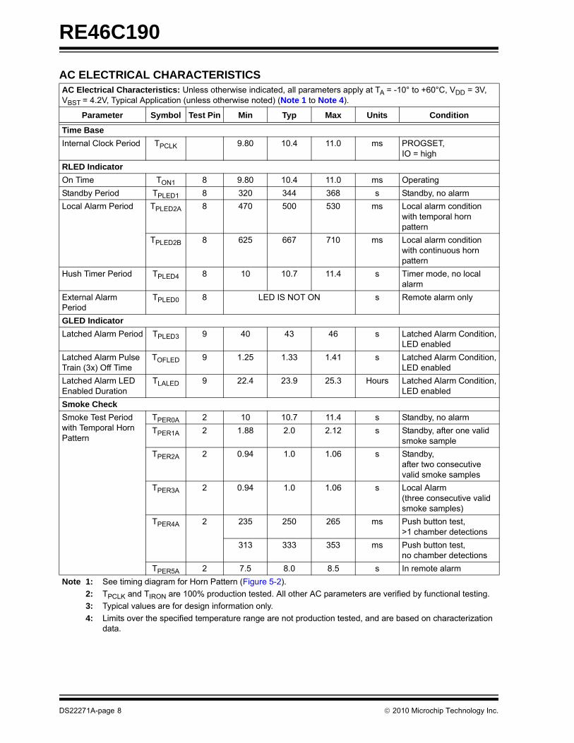
RE46C190
AC ELECTRICAL CHARACTERISTICSAC Electrical Characteristics: Unless otherwise indicated, all parameters apply at TA = -10° to +60°C, VDD = 3V, VBST = 4.2V, Typical Application (unless otherwise noted) (Note 1 to Note 4).
Parameter Symbol Test Pin Min Typ Max Units Condition
Time Base
Internal Clock Period TPCLK 9.80 10.4 11.0 ms PROGSET, IO = high
RLED Indicator
On Time TON1 8 9.80 10.4 11.0 ms Operating
Standby Period TPLED1 8 320 344 368 s Standby, no alarm
Local Alarm Period TPLED2A 8 470 500 530 ms Local alarm condition with temporal horn pattern
TPLED2B 8 625 667 710 ms Local alarm condition with continuous hornpattern
Hush Timer Period TPLED4 8 10 10.7 11.4 s Timer mode, no local alarm
External Alarm Period
TPLED0 8 LED IS NOT ON s Remote alarm only
GLED Indicator
Latched Alarm Period TPLED3 9 40 43 46 s Latched Alarm Condition,LED enabled
Latched Alarm Pulse Train (3x) Off Time
TOFLED 9 1.25 1.33 1.41 s Latched Alarm Condition,LED enabled
Latched Alarm LED Enabled Duration
TLALED 9 22.4 23.9 25.3 Hours Latched Alarm Condition,LED enabled
Smoke Check
Smoke Test Periodwith Temporal Horn Pattern
TPER0A 2 10 10.7 11.4 s Standby, no alarm
TPER1A 2 1.88 2.0 2.12 s Standby, after one valid smoke sample
TPER2A 2 0.94 1.0 1.06 s Standby,after two consecutive valid smoke samples
TPER3A 2 0.94 1.0 1.06 s Local Alarm(three consecutive valid smoke samples)
TPER4A 2 235 250 265 ms Push button test, >1 chamber detections
313 333 353 ms Push button test, no chamber detections
TPER5A 2 7.5 8.0 8.5 s In remote alarm
Note 1: See timing diagram for Horn Pattern (Figure 5-2).
2: TPCLK and TIRON are 100% production tested. All other AC parameters are verified by functional testing.
3: Typical values are for design information only.
4: Limits over the specified temperature range are not production tested, and are based on characterization data.
DS22271A-page 8 2010 Microchip Technology Inc.

RE46C190
Smoke Test Periodwith Continuous Horn Pattern
TPER0B 2 10 10.7 11.4 s Standby, no alarm
TPER1B 2 2.5 2.7 2.9 s Standby, after one valid smoke sample
TPER2B 2 1.25 1.33 1.41 s Standby,after two consecutive valid smoke samples
TPER3B 2 1.25 1.33 1.41 s Local Alarm(three consecutive valid smoke samples)
TPER4B 2 313 333 353 ms Push button test
TPER5B 2 10 10.7 11.4 s In remote alarm
Chamber Test Period TPCT1 2 40 43 46 s Standby, no alarm
Long Term Drift Sample Period
TLTD 2 400 430 460 s Standby, no alarmLTD enabled
Low Battery
Low Battery Sample Period
TPLB1 3 320 344 368 s RLED on
TPLB2 3 80 86 92 s RLED on
Horn Operation
Low Battery Horn Period
THPER1 13 40 43 46 s Low battery, no alarm
Chamber Fail Horn Period
THPER2 13 40 43 46 s Chamber failure
Low Battery Horn On Time
THON1 13 9.8 10.4 11.0 ms Low battery, no alarm
Chamber Fail Horn On Time
THON2 13 9.8 10.4 11.0 ms Chamber failure
Chamber Fail Off Time
THOF1 13 305 325 345 ms Failed chamber, no alarm, 3x chirp option
Alarm On Time with Temporal Horn Pattern
THON2A 13 470 500 530 ms Local or remote alarm (Note 1)
Alarm Off Time with Temporal Horn Pattern
THOF2A 13 470 500 530 ms Local or remote alarm (Note 1)
THOF3A 13 1.4 1.5 1.6 s Local or remote alarm (Note 1)
Alarm On Time with Continuous Horn Pattern
THON2B 13 235 250 265 ms Local or remote alarm (Note 1)
Alarm Off Time with Continuous Horn Pattern
THOF2B 13 78 83 88 ms Local or remote alarm (Note 1)
AC ELECTRICAL CHARACTERISTICS (CONTINUED)AC Electrical Characteristics: Unless otherwise indicated, all parameters apply at TA = -10° to +60°C, VDD = 3V, VBST = 4.2V, Typical Application (unless otherwise noted) (Note 1 to Note 4).
Parameter Symbol Test Pin Min Typ Max Units Condition
Note 1: See timing diagram for Horn Pattern (Figure 5-2).
2: TPCLK and TIRON are 100% production tested. All other AC parameters are verified by functional testing.
3: Typical values are for design information only.
4: Limits over the specified temperature range are not production tested, and are based on characterization data.
2010 Microchip Technology Inc. DS22271A-page 9

RE46C190
Push-to-Test Alarm Memory On Time
THON4 13 9.8 10.4 11.0 ms Alarm memory active, push-to-test
Push-to-Test Alarm Memory Horn Period
THPER4 13 235 250 265 ms Alarm memory active, push-to-test
Interconnect Signal Operation (IO)
IO Active Delay TIODLY1 12 — 0 — s From start of local alarm to IO active
Remote Alarm Delay with Temporal Horn Pattern
TIODLY2A 12 0.780 1.00 1.25 s No local alarm, from IO active to alarm
Remote Alarm Delay with Continuous Horn Pattern
TIODLY2B 12 380 572 785 ms No local alarm, from IO active to alarm
IO Charge Dump Duration
TIODMP 12 1.23 1.31 1.39 s At conclusion of local alarm or test
IO Filter TIOFILT 12 — — 313 ms Standby, no alarm
Hush Timer Operation
Hush Timer Period TTPER 8.0 8.6 9.1 Min No alarm
EOL
End-of-Life Age Sample
TEOL 314 334 354 Hours EOL Enabled; Standby
Detection
IRED On Time TIRON 2 — 100 — µs Prog Bits 3,4 = 1,12 — 200 — µs Prog Bits 3,4 = 0,12 — 300 — µs Prog Bits 3,4 = 1,02 — 400 — µs Prog Bits 3,4 = 0,0
TEMPERATURE CHARACTERISTICSElectrical Specifications: All limits specified for VDD = 3V, VBST = 4.2V and VSS = 0V, Except where noted in the Electrical Characteristics.
Parameters Sym Min Typ Max Units Conditions
Temperature Ranges
Operating Temperature Range TA -10 — +60 °C
Storage Temperature Range TSTG -55 — +125 °C
Thermal Package Resistances
Thermal Resistance, 16L-SOIC (150 mil.) θJA — 86.1 — °C/W
AC ELECTRICAL CHARACTERISTICS (CONTINUED)AC Electrical Characteristics: Unless otherwise indicated, all parameters apply at TA = -10° to +60°C, VDD = 3V, VBST = 4.2V, Typical Application (unless otherwise noted) (Note 1 to Note 4).
Parameter Symbol Test Pin Min Typ Max Units Condition
Note 1: See timing diagram for Horn Pattern (Figure 5-2).
2: TPCLK and TIRON are 100% production tested. All other AC parameters are verified by functional testing.
3: Typical values are for design information only.
4: Limits over the specified temperature range are not production tested, and are based on characterization data.
DS22271A-page 10 2010 Microchip Technology Inc.

RE46C190
2.0 PIN DESCRIPTIONS
The descriptions of the pins are listed in Table 2-1.
TABLE 2-1: PIN FUNCTION TABLE
RE46C190SOIC
Symbol Function
1 VSS Connect to the negative supply voltage.
2 IRED Provides a regulated and programmable pulsed current for the infrared emitter diode.
3 VDD Connect to the positive supply or battery voltage.
4 TEST This input is used to invoke Test modes and the Timer mode. This input has an internal pull-down.
5 TEST2 Test input for test and programming modes. This input has an internal pull-down.
6 IRP Connect to the anode of the photo diode.
7 IRN Connect to the cathode of the photo diode.
8 RLED Open drain NMOS output, used to drive a visible LED. This pin provides load current for the low battery test, and is a visual indicator for Alarm and Hush modes.
9 GLED Open drain NMOS output used to drive a visible LED to provide visual indication of an Alarm Memory condition.
10 FEED Usually connected to the feedback electrode through a current limiting resistor. If not used, this pin must be connected to VDD or VSS.
11 IRCAP Used to charge and monitor the IRED capacitor.
12 IO This bidirectional pin provides the capability to interconnect many detectors in a single system. This pin has an internal pull-down device and a charge dump device.
13 HB This pin is connected to the metal electrode of a piezoelectric transducer.
14 HS This pin is a complementary output to HB, connected to the ceramic electrode of the piezoelectric transducer.
15 VBST Boosted voltage produced by DC-DC converter.
16 LX Open drain NMOS output, used to drive the boost converter inductor. The inductor should be connected from this pin to the positive supply through a low resistance path.
2010 Microchip Technology Inc. DS22271A-page 11

RE46C190
NOTES:
DS22271A-page 12 2010 Microchip Technology Inc.

RE46C190
3.0 DEVICE DESCRIPTION
3.1 Standby Internal Timing
The internal oscillator is trimmed to ±6% tolerance.Once every 10 seconds, the boost converter ispowered up, the IRcap is charged from VBST and thenthe detection circuitry is active for 10 ms. Prior tocompletion of the 10 mS period, the IRED pulse isactive for a user-programmable duration of 100-400 µs. During this IRED pulse, the photo diode currentis integrated and then digitized. The result is comparedto a limit value stored in EEPROM during calibration todetermine the photo chamber status. If a smokecondition is present, the period to the next detectiondecreases, and additional checks are made.
3.2 Smoke Detection Circuitry
The digitized photo amplifier integrator output iscompared to the stored limit value at the conclusion ofthe IRED pulse period. The IRED drive is all internal,and both the period and current are userprogrammable. Three consecutive smoke detectionswill cause the device to go into Alarm and activate thehorn and interconnect circuits. In Alarm, the horn isdriven at the high boost voltage level, which isregulated based on an internal voltage reference, andtherefore results in consistent audibility over batterylife. RLED will turn on for 10 ms at a 2 Hz rate. In LocalAlarm, the integration limit is internally decreased toprovide alarm hysteresis. The integrator has threeseparate gain settings:
• Normal and Hysteresis • Reduced Sensitivity (HUSH) • High Gain for Chamber Test and Push-to-Test
There are four separate sets of integration limits (alluser programmable):
• Normal Detection
• Hysteresis
• HUSH
• Chamber Test and Push-to-Test modes
In addition, there are user selectable integrator gainsettings to optimize detection levels (see Table 4-1).
3.3 Supervisory Tests
Once every 86 seconds, the status of the batteryvoltage is checked by enabling the boost converter for10 ms and comparing a fraction of the VDD voltage toan internal reference. In each period of 344 seconds,the battery voltage is checked four times. Three checksare unloaded and one check is performed with theRLED enabled, which provides a battery load. TheHigh Boost mode is active only for the loaded lowbattery test. In addition, once every 43 seconds thechamber is activated and a High Gain mode andchamber test limits are internally selected. A check ofthe chamber is made by amplifying backgroundreflections. The Low Boost mode is used for thechamber test.
If either the low battery test or the chamber test fails,the horn will pulse on for 10 ms every 43 seconds, andwill continue to pulse until the failing condition passes.If two consecutive chamber tests fail, the horn will pulseon three times for 10 ms, separated by 330 ms every43 seconds. Each of the two supervisory test audibleindicators is separated by approximately 20 seconds.
As an option, a Low Battery Silence mode can beinvoked. If a low battery condition exists, and the TESTinput is driven high, the RLED will turn on. If the TESTinput is held for more than 0.5 second, the unit willenter the Push-to-test operation described inSection 3.4 “Push-to-Test Operation (PTT)”. Afterthe TEST input is driven low, the unit enters in LowBattery Hush mode, and the 10 ms horn pulse issilenced for 8 hours. The activation of the test buttonwill also initiate the 9 minute Reduced Sensitivity modedescribed in Section 3.6 “Reduced SensitivityMode”. At the end of the 8 hours, the audible indicationwill resume if the low battery condition still exists.
3.4 Push-to-Test Operation (PTT)
If the TEST input pin is activated (VIH), the smokedetection rate increases to once every 250 ms afterone internal clock cycle. In Push-to-Test, the photoamplifier High Gain mode is selected, and backgroundreflections are used to simulate a smoke condition.After the required three consecutive detections, thedevice will go into a Local Alarm condition. When theTEST input is driven low (VIL), the photo amplifierNormal Gain is selected, after one clock cycle. Thedetection rate continues at once every 250 ms untilthree consecutive No Smoke conditions are detected.At this point, the device returns to standby timing. Inaddition, after the TEST input goes low, the deviceenters the HUSH mode (see Section 3.6 “ReducedSensitivity Mode”).
2010 Microchip Technology Inc. DS22271A-page 13

RE46C190
3.5 Interconnect Operation
The bidirectional IO pin allows the interconnection ofmultiple detectors. In a Local Alarm condition, this pinis driven high (High Boost) immediately through aconstant current source. Shorting this output to groundwill not cause excessive current. The IO is ignored asinput during a Local Alarm.
The IO pin also has an NMOS discharge device that isactive for 1.3 seconds after the conclusion of any typeof Local Alarm. This device helps to quickly dischargeany capacitance associated with the interconnect line.
If a remote, active high signal is detected, the devicegoes into Remote Alarm and the horn will be active.RLED will be off, indicating a Remote Alarm condition.Internal protection circuitry allows the signaling unit tohave a higher supply voltage than the signaled unit,without excessive current draw.
The interconnect input has a 336 ms nominal digitalfilter. This allows the interconnection to other types ofalarms (carbon monoxide, for example) that may havea pulsed interconnect signal.
3.6 Reduced Sensitivity Mode
A Reduced Sensitivity or Hush mode is initiated byactivating the TEST input (VIH). If the TEST input isactivated during a Local Alarm, the unit is immediatelyreset out of the alarm condition, and the horn issilenced. When the TEST input is deactivated (VIL), thedevice enters into a 9-minute nominal Hush mode.During this period, the HUSH integration limit isselected. The hush gain is user programmable. InReduced Sensitivity mode, the RLED flashes for 10 msevery 10 seconds to indicate that the mode is active.As an option, the Hush mode will be cancelled if any ofthe following conditions exist:
• Reduced sensitivity threshold is exceeded (high smoke level)
• An interconnect alarm occurs
• TEST input is activated again
3.7 Local Alarm Memory
An Alarm Memory feature allows easy identification ofany unit that had previously been in a Local Alarmcondition. If a detector has entered a Local Alarm,when it exits that Local Alarm, the Alarm Memory latchis set. Initially the GLED can be used to visually identifyany unit that had previously been in a Local Alarmcondition. The GLED flashes three times spaced1.3 seconds apart. This pattern will repeat every43 seconds. The duration of the flash is 10 ms. In orderto preserve battery power, this visual indication will stopafter a period of 24 hours. The user will still be able toidentify a unit with an active alarm memory by pressingthe Push-to-Test button. When this button is active, thehorn will chirp for 10 ms every 250 ms.
If the Alarm Memory condition is set, then any time thePush-to-Test button is pressed and released, the AlarmMemory latch is reset.
The initial 24 hour visual indication is not displayed if alow battery condition exists.
3.8 End of Life Indicator
As an option, after every 14 days of continuousoperation, the device will read a stored age count fromthe EEPROM and increment this count. After 10 yearsof powered operation, an audible warning will occurindicating that the unit should be replaced. Thisindicator will be similar to the chamber test failurewarning in that the horn will pulse on three times for10 ms separated by 330 ms every 43 seconds. Thisindicator will be separated from the low batteryindicator by approximately 20 seconds.
3.9 Photo Chamber Long Term Drift Adjustment
As an option, the design includes a Long Term DriftAdjustment for the photo chamber. If this option isselected, during calibration a normal no-smokebaseline integration measurement is made and storedin EEPROM. During normal operation, a new baselineis calculated by making 64 integration measurementsover a period of 8 hours. These measurements areaveraged and compared to the original baseline storedduring calibration to calculate the long term drift. Allfour limits stored during calibration are adjusted by thisdrift factor. Drift sampling is suspended during Hush,Local Smoke and Remote Smoke conditions.
DS22271A-page 14 2010 Microchip Technology Inc.

RE46C190
4.0 USER PROGRAMMING MODES
TABLE 4-1: PARAMETRIC PROGRAMMING
Parametric Programming Range Resolution
IRED Period 100-400 µs 100 µs
IRED Current Sink 50-200 mA 50 mA
Low Battery Detection Voltage 2.1 – 2.8V 100 mV
Photo Detection Limits Typical Maximum Input Current (nA)
100 µs 200 µs 300 µs 400 µs
Normal/Hysteresis GF = 1 58 29 19.4 14.5
GF = 2 29 14.5 9.6 7.2
GF = 3 14.5 7.2 4.8 3.6
GF = 4 7.2 3.6 2.4 1.8
Hush GF = 1 116 58 38.8 29
GF = 2 58 29 19.4 14.5
GF = 3 29 14.5 9.6 7.2
GF = 4 14.5 7.2 4.8 3.6
Chamber Test GF = 1 29 14.5 9.6 7.2
GF = 2 14.5 7.2 4.8 3.6
GF = 3 7.2 3.6 2.4 1.8
GF = 4 3.6 1.8 1.2 0.9
Note 1: GF is the user selectable Photo Integration Gain Factor. Once selected, it applies to all modes of operation. For example, if GF = 1 and integration time is selected to be 100 µs, the ranges will be as follows: Normal/Hysteresis = 58 nA, Hush = 116 nA, Chamber Test = 29 nA.
2: Nominal measurement resolution in each case will be 1/31 of the maximum input range.
3: The same current resolution and ranges applies to the limits.
TABLE 4-2: FEATURES PROGRAMMING
Features Options
Tone Select Continuous or NFPA Tone
10 Year End-of-life Indicator Enable/Disable
Photo Chamber Long Term Drift Adjustment Enable/Disable
Low Battery Hush Enable/Disable
Hush Options Option 1: Hush mode is not cancelled for any reason. If the test button is pushed during Hush, the unit reverts to Normal Sensitivity to test the unit, but when it comes out of test, resumes in Hush where it left off.
Option 2: The Hush mode is cancelled if the Reduced Sensitivity threshold is exceeded (high smoke level), and if an external (interconnect alarm) is signaled. If the test button is pushed during Hush, after the test is executed, the Hush mode is terminated.
2010 Microchip Technology Inc. DS22271A-page 15

RE46C190
4.1 Calibration and Programming Procedures
Eleven separate programming and test modes areavailable for user customization. To enter these modes,after power-up, TEST2 must be driven to VDD and heldat that level. The TEST input is then clocked to stepthrough the modes. FEED and IO are reconfigured tobecome test mode inputs, while RLED, GLED and HBbecome test mode outputs. The test mode functions foreach pin are outlined in Table 4-3.
When TEST2 is held at VDD, TEST becomes a tri-stateinput with nominal input levels at VSS, VDD and VBST. ATEST clock occurs whenever the TEST input switchesfrom VSS to VBST. The TEST Data column representsthe state of TEST when used as a data input, whichwould be either VSS or VDD. The TEST pin cantherefore be used as both a clock, to change modes,and a data input, once a mode is set. Other pinfunctions are described in Section 4.2 “UserSelections”.
TABLE 4-3: TEST MODE FUNCTIONS
Mo
de
DescriptionTEST Clock
TEST Data
TEST2 FEED IO RLED GLED HB
VIH VBST VDD VDD VBST VDD — — —
VIL VSS VSS VSS VSS VSS — — —
T0 Photo Gain Factor (2 bits)
0 ProgData VDD ProgCLK ProgEn 14 bits RLED GLED HB
Integ Time (2 bits) 0 ProgData VDD ProgCLK ProgEn 14 bits RLED GLED HB
IRED Current (2 bits) 0 ProgData VDD ProgCLK ProgEn 14 bits RLED GLED HB
Low Battery Trip (3 bits)
0 ProgData VDD ProgCLK ProgEn 14 bits RLED GLED HB
LTD Enable (1 bit) 0 ProgData VDD ProgCLK ProgEn 14 bits RLED GLED HB
Hush Option (1 bit) 0 ProgData VDD ProgCLK ProgEn 14 bits RLED GLED HB
LB Hush Enable (1 bit)
0 ProgData VDD ProgCLK ProgEn 14 bits RLED GLED HB
EOL Enable (1 bit) 0 ProgData VDD ProgCLK ProgEn 14 bits RLED GLED HB
Tone Select (1 bit) 0 ProgData VDD ProgCLK ProgEn 14 bits RLED GLED HB
T1 Norm Lim Set (5 bits)( 4)
1 not used VDD CalCLK LatchLim( 3) Gamp IntegOut SmkComp( 1)
T2 Hyst Lim Set (5 bits)( 4)
2 not used VDD CalCLK LatchLim( 3) Gamp IntegOut SmkComp( 1)
T3 Hush Lim Set (5 bits)( 4)
3 not used VDD CalCLK LatchLim( 3) Gamp IntegOut SmkComp( 1)
T4 Ch Test Lim Set (5 bits)( 4)
4 not used VDD CalCLK LatchLim( 3) Gamp IntegOut SmkComp( 1)
T5 LTD Baseline (5 bits) 5 not used VDD MeasEn ProgEn 25 bits Gamp IntegOut SmkComp( 1)
T6 Serial Read/Write 6 ProgData VDD ProgCLK ProgEn RLED GLED Serial Out
T7 Norm Lim Check 7 not used VDD MeasEn not used Gamp IntegOut SCMP( 2)
T8 Hyst Lim Check 8 not used VDD MeasEn not used Gamp IntegOut SCMP( 2)
T9 Hush Lim Check 9 not used VDD MeasEn not used Gamp IntegOut SCMP( 2)
T10 Ch Test Lim Check 10 not used VDD MeasEn not used Gamp IntegOut SCMP( 2)
T11 Horn Test 11 not used VDD FEED HornEn RLED GLED HB
Note 1: SmkComp (HB) – digital comparator output (high if Gamp < IntegOut; low if Gamp > IntegOut)
2: SCMP (HB) – digital output representing comparison of measurement value and associated limit. Signal is valid only after MeasEn has been asserted and measurement has been made. (SCMP high if measured value > limit; low if measured value < limit).
3: LatchLim (IO) – digital input used to latch present state of limits (Gamp level) for later storage. T1-T4 limits are latched, but not stored until ProgEn is asserted in T5 mode.
4: Operating the circuit in this manner with nearly continuous IRED current for an extended period of time may result in undesired or excessive heating of the part. The duration of this step should be minimized.
DS22271A-page 16 2010 Microchip Technology Inc.
RE46C190
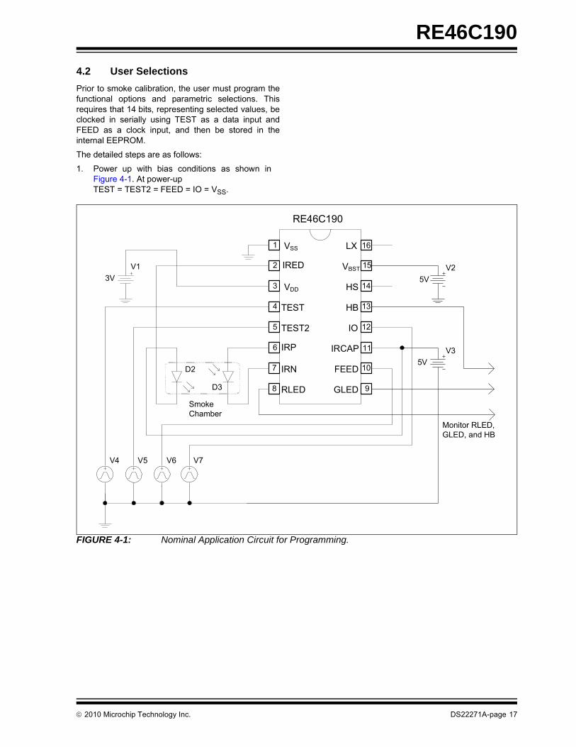
4.2 User Selections
Prior to smoke calibration, the user must program thefunctional options and parametric selections. Thisrequires that 14 bits, representing selected values, beclocked in serially using TEST as a data input andFEED as a clock input, and then be stored in theinternal EEPROM.
The detailed steps are as follows:
1. Power up with bias conditions as shown inFigure 4-1. At power-upTEST = TEST2 = FEED = IO = VSS.
FIGURE 4-1: Nominal Application Circuit for Programming.
16
15
14
13
12
11
10
98
7
6
5
4
3
2
1 VSS
IRED
VDD
TEST
TEST2
IRP
IRN
RLED
FEED
GLED
IRCAP
IO
HB
HS
VBST
LX
RE46C190
V1
3V
V4 V5 V6 V7
Smoke Chamber
D2
D3
V2
5V
V3
5V
Monitor RLED, GLED, and HB
2010 Microchip Technology Inc. DS22271A-page 17

RE46C190
2. Drive TEST2 input from VSS to VDD and hold atVDD through Step 5 below.
3. Using TEST as data and FEED as clock, shift invalues as selected from Register 4-1.
Note: For test mode T0 only 14 bits (bits 25-38)will be loaded. For test mode T6 all 39 bits(bits 0-38), will be loaded.
REGISTER 4-1: CONFIGURATION AND CALIBRATION SETTINGS REGISTER
W-x W-x W-x W-x W-x W-x W-x
TS EOL LBH HUSH LTD LB0 LB1
bit 38 bit 32
W-x W-x W-x W-x W-x W-x W-x W-x
LB2 IRC1 IRC0 IT1 IT0 PAGF1 PAGF0 NL4
bit 31 bit 24
W-x W-x W-x W-x W-x W-x W-x W-x
NL3 NL2 NL1 NL0 HYL4 HYL3 HYL2 HYL1
bit 23 bit 16
W-x W-x W-x W-x W-x W-x W-x W-x
HYL0 HUL4 HUL3 HUL2 HUL1 HUL0 CTL4 CTL3
bit 15 bit 8
W-x W-x W-x W-x W-x W-x W-x W-x
CTL2 CTL1 CTL0 LTD4 LTD3 LTD2 LTD1 LTD0
bit 7 bit 0
Legend:
R = Readable bit W = Writable bit U = Unimplemented bit, read as ‘0’
-n = Value at POR ‘1’ = Bit is set ‘0’ = Bit is cleared x = Bit is unknown
bit 38 TS: Tone Select bit
1 = Temporal Horn Pattern0 = Continuous Horn Pattern
bit 37 EOL: End of Life Enable bit
1 = Enable0 = Disable
bit 36 LBH: Low Battery Hush Enable bit
1 = Enable0 = Disable
bit 35 HUSH: Hush Option bit
1 = Cancelled for high smoke level, interconnect alarm, or second push of TEST button (as described above)
0 = Never Cancel
bit 34 LTD: Long Term Drift Enable bit
1 = Enable0 = Disable
DS22271A-page 18 2010 Microchip Technology Inc.

RE46C190
bit 33-31 LB<0:2>: Low Battery Trip Point bits
000 = 2.1V001 = 2.5V010 = 2.3V011 = 2.7V100 = 2.2V101 = 2.6V110 = 2.4V111 = 2.8V
bit 30-29 IRC<1:0>: IRED Current bits
00 = 50 mA01 = 100 mA10 = 150 mA11 = 200 mA
bit 28-27 IT<1:0>: Integration Time bits
00 = 400 µs01 = 300 µs10 = 200 µs11 = 100 µs
bit 26-25 PAGF<1:0>: Photo Amplifier Gain Factor bits
00 = 101 = 210 = 311 = 4
bit 24-20 NL<4:0>: Normal Limits bits (Section 3.2)
00000 =000001 =1
•
•
•
11110 =3011111 =31
bit 19-15 HYL<4:0>: Hysteresis Limits bits (Section 3.2)
00000 =000001 =1
•
•
•
11110 =3011111 =31
bit 14-10 HUL<4:0>: Hush Limits bits (Section 3.6)
00000 =000001 =1
•
•
•
11110 =3011111 =31
REGISTER 4-1: CONFIGURATION AND CALIBRATION SETTINGS REGISTER (CONTINUED)
2010 Microchip Technology Inc. DS22271A-page 19

RE46C190
The minimum pulse width for FEED is 10 µs, while theminimum pulse width for TEST is 100 µs. For example,for the following options, the sequence would be:
4. After shifting in data, pull IO input to VDD, thenVSS (minimum pulse width of 10 ms) to storeshift register contents into the memory.
5. If any changes are required, power down thepart and return to Step 1. All bit values must bereentered.
FIGURE 4-2: Timing Diagram for Mode T0.
bit 9-5 CTL<4:0>: Chamber Test Limits bits (Section 3.3)
00000 =000001 =1
•
•
•
11110 =3011111 =31
bit 4-0 LTD<4:0>: Long Term Drift Sample bits (Section 3.9)
00000 =000001 =1
•
•
•
11110 =3011111 =31
REGISTER 4-1: CONFIGURATION AND CALIBRATION SETTINGS REGISTER (CONTINUED)
data - 0 0 0 1 1 0 0 0 1 0 0 0 0 1
bit - 25 26 27 28 29 30 31 32 33 34 35 36 37 38
Photo Amp Gain Factor = 1
Integration Time = 200 µs
IRED Current = 100 mA
Low Battery Trip = 2.2V
Long Term Drift, Low Battery Hush and EOL are all disabled
Hush Option = Never Cancel
Tone Select = Temporal
VDD
TEST2VSS
VDD
TEST bit 25 bit 26 bit 27 bit 28 bit 29 bit 30 bit 31 bit 32 bit 33 bit 34 bit 35 bit 36 bit 37 bit 38VSS
VBST
FEEDVSS
Min Tsetup2 = 2 µs Min Tsetup1 = 1 µs Min Thold1 = 1 µs Min PW1 = 10us Min T1 = 20 µs Min Td1 = 2 µs
VDD
IO …VSS
Min PW2 = 10 ms
DS22271A-page 20 2010 Microchip Technology Inc.

RE46C190
As an alternative to Figure 4-1, Figure 4-3 can be usedto program while in the application circuit. Note that inaddition to the five programming supplies, connectionsto VSS are needed at TP1 and TP2.
FIGURE 4-3: Circuit for Programming in the Typical Application.
330
VBST
16
15
14
13
12
11
10
98
7
6
5
3
2
1 VSS
IRED
VDD
TEST
TEST2
IRP
IRN
RLED
FEED
GLED
IRCAP
IO
HB
HS
VBST
LX
RE46C190
D2
D3
4
9
D1
4.7 µF
C4200K
R3
1.5M
R41 nF
C5
L110 µH
330R5
33 µF
C6
To other Units
1 µFC2
100
R1
10 µFC1
VDD
VBST
R6100R7
D4
RED
D5
GREEN
C3
100 µF
SmokeChamber
V1
3V
TP1 TP2
V4 V5 V6 V7
V2
5V
V3
5V
Monitor RLED, GLED and HB
Push-To-Test/Hush
2010 Microchip Technology Inc. DS22271A-page 21
RE46C190
4.3 Smoke Calibration
A separate calibration mode is entered for eachmeasurement mode (Normal, Hysteresis, Hush andChamber Test) so that independent limits can be set foreach. In all calibration modes, the integrator output canbe accessed at the GLED output.
The Gamp output voltage, which represents the smokedetection level, can be accessed at the RLED output.The SmkComp output voltage is the result of thecomparison of Gamp with the integrator output, andcan be accessed at HB. The FEED input can beclocked to step up the smoke detection level at RLED.Once the desired smoke threshold is reached, theTEST input is pulsed low to high to store the result.
The procedure is described in the following steps:
1. Power up with the bias conditions shown inFigure 4-1.
2. Drive TEST2 input from VSS to VDD to enter theProgramming mode. TEST2 should remain atVDD through Step 8 described below.
3. Apply a clock pulse to the TEST input to enter inT1 mode. This initiates the calibration mode forNormal Limits setting. The Integrator output sawtooth should appear at GLED and the smokedetection level at RLED. Clock FEED toincrease the smoke detection level as needed.Once the desired smoke threshold is reached,the IO input is pulsed low to high to enter theresult. See typical waveforms in Figure 4-4.Operating the circuit in this manner, with nearlycontinuous IRED current for an extended periodof time, may result in undesired or excessiveheating of the part. The duration of this stepshould be minimized.
4. Apply a second clock pulse to the TEST input toenter in T2 mode. This initiates the calibrationmode for Hysteresis Limits. Clock FEED as inStep 3 and apply pulse to IO, once desired levelis reached.Operating the circuit in this manner,with nearly continuous IRED current for anextended period of time, may result in undesiredor excessive heating of the part. The duration ofthis step should be minimized.
5. Apply a clock pulse to the TEST input again toenter in T3 mode and initiate calibration for HushLimits. Clock FEED as in the steps above andapply a pulse to IO, once the desired level isreached. Operating the circuit in this manner,with nearly continuous IRED current for anextended period of time, may result in undesiredor excessive heating of the part. The duration ofthis step should be minimized.
6. Apply a clock pulse to the TEST input a fourthtime to enter in T4 mode, and initiate thecalibration for Chamber Test Limits. Clock FEEDand apply pulse to IO, once desired level isreached. Operating the circuit in this manner,with nearly continuous IRED current for anextended period of time, may result in undesiredor excessive heating of the part. The duration ofthis step should be minimized.
7. If the Long Term Drift Adjustment is enabled,after all limits have been set, the long term drift(LTD) baseline measurement must be made. Todo this, a measurement must be made underno-smoke conditions. To enable the baselinemeasurement, pull TEST from VSS to VBSTagain and return to VSS. Once the chamber isclear, pulse FEED low to high to make thebaseline measurement.
8. After limits have been set and baseline LTDmeasurement has been made, pulse IO to storeall results in memory. Before this step, no limitsare stored in memory.
DS22271A-page 22 2010 Microchip Technology Inc.

RE46C190
FIGURE 4-4: Timing Diagram for Modes T1 to T5.
VDD
TEST2VSS
Min Tsetup2 = 2 µs
VBST
TESTVSS
Min PW3 = 100 µs
VBST
FEEDVSS
Min Td2 = 10 µs Min PW1 = 10 µs Min T1 = 20 µs Min PW5 = 2 ms
VDD
IOVSS
Min PW2 = 10 ms
GLED … … … …
IRED … … … …
HB
RLED
2010 Microchip Technology Inc. DS22271A-page 23

RE46C190
4.4 Serial Read/Write
As an alternative to the steps in Section 4.3 “SmokeCalibration”, if the system has been wellcharacterized, the limits and baseline can be entereddirectly from a serial read/write calibration mode.
To enter this mode, follow these steps:
1. Set up the application as shown in Figure 4-1.
2. Drive TEST2 input from VSS to VDD to enter inProgramming mode. TEST2 should remain atVDD until all data has been entered.
3. Clock the TEST input to mode T6 (High = VBST,Low = VSS, 6 clocks). This enables the serialread/write mode.
4. TEST now acts as a data input (High = VDD,Low = VSS). FEED acts as the clock input(High = VBST, Low = VSS). Clock in the limits,LTD baseline, functional and parametricoptions. The data sequence should be asfollows:
Then, the data sequence follows the pattern describedin Register 4-1:
A serial data output is available at HB.
5. After all 39 bits have been entered, pulse IO tostore into the EEPROM memory.
FIGURE 4-5: Timing Diagram for Mode T6.
5 bit LTD sample (LSB first)
5 bit Chamber Test Limits (LSB first)
5 bit Hush Limits (LSB first)
5 bit Hysteresis Limits (LSB first),
5 bit Normal Limits (LSB first)
2 bit Photo Amp Gain Factor
2 bit Integration Time
2 bit IRED current
3 bit Low Battery Trip Point
1 bit Long Term Drift Enable
1 bit Hush Option
1 bit Low Battery Hush Enable
1 bit EOL enable
1 bit Tone Select
VDD
TEST2VSS
VBST
TEST D1 D2 D3 D4 D5 D6 D7 D8 D9 D10 D11 D12 D13 D14 D15 … D39VSS VSS
Min Tsetup2 = 2 µs Min PW3 = 100 µs Min T2 = 120 µs
VBST
FEED …VSS
Min Tsetup1 = 1 µs Min Thold1 = 1 µs Min PW1 = 10 µs Min T1 = 20 µs
VDD
IO …VSS
Min PW2 = 10 ms
DS22271A-page 24 2010 Microchip Technology Inc.

RE46C190
4.5 Limits Verification
After all limits and LTD baseline have been entered andstored into the memory, additional test modes areavailable to verify if the limits are functioning asexpected. Table 4-4 describes several verificationtests.
FIGURE 4-6: Timing Diagram for Modes T7-T10.
TABLE 4-4: LIMITS VERIFICATION DESCRIPTION
Limit Test Description
Normal Limits Clock TEST to Mode T7 (7 clocks). With appropriate smoke level in chamber, pull FEED to VDD and hold for at least 1 ms. The HB output will indicate the detection status (High = smoke detected).
Hysteresis Limits Clock TEST to Mode T8 (8 clocks). Pulse FEED and monitor HB as in Normal Limits case.
Hush Limits Clock TEST to Mode T9 (9 clocks). Pulse FEED and monitor HB.
Chamber Test Limits Clock TEST to Mode T10 (10 clocks). Pulse FEED and monitor HB.
VDD
TEST2VSS
VBST
TESTVSS
Min Tsetup2 = 2 µs Min PW3 = 100 µs Min T2 = 120 µs
Vbst
FEEDVSS
Min Td2 = 10 µs Min PW5 = 2 ms
VDD
IOVSS
GLED … … …
IRED … … …
HB
RLED
2010 Microchip Technology Inc. DS22271A-page 25

RE46C190
4.6 Horn Test
The last test mode allows the horn to be enabledindefinitely for audibility testing. To enter this mode,clock TEST to Mode T11 (11 clocks). The IO pin isconfigured as horn enable.
FIGURE 4-7: Timing Diagram for Mode T11.
VDD
TEST2VSS
VBST
TESTVSS
Min Tsetup2 = 2 µs Min PW3 = 100 µs Min T2 = 120 µs
VDD
IOVSS
Horn Enabled
DS22271A-page 26 2010 Microchip Technology Inc.

RE46C190
5.0 APPLICATION NOTES
5.1 Standby Current Calculation and Battery Life
The supply current shown in the DC ElectricalCharacteristics table is only one component of theaverage standby current and, in most cases, can be asmall fraction of the total, because power consumptiongenerally occurs in relatively infrequent bursts anddepends on many external factors. These include thevalues selected for IRED current and integration time,the VBST and IR capacitor sizes and leakages, the VBATlevel, and the magnitude of any external resistancesthat will adversely affect the boost converter efficiency.
A calculation of the standby current for the battery lifeis shown in Table 5-1, based on the followingparameters:
The following paragraphs explain the components inTable 5-1, and the calculations in the example.
5.1.1 FIXED IDD
The IDD is the Supply Current shown in the DCElectrical Characteristics table.
5.1.2 PHOTO DETECTION CURRENT
Photo Detection Current is the current draw due to thesmoke testing every 10.75 seconds, and the chambertest every 43 seconds. The current for both the IRdiode and the internal measurement circuitry comesprimarily from VBST, so the average current must bescaled for both on-time and boost voltage.
The contribution to IBAT is determined by firstcalculating the energy consumed by each component,given its duration. An average power is then calculatedbased on the period of the event and the boostconverter efficiency (assumed to be 85% in this case).An IBAT contribution is then calculated based on thisaverage power and the given VBAT. For example, the IRdrive contribution during chamber test is detailed inEquation 5-1:
EQUATION 5-1:
VBAT = 3
VBST1 = 3.6
VBST2 = 9
Boost capacitor size = 4.70E-06
Boost Efficiency = 8.50E-01
IRED on time = 2.000E-04
IRED Current = 1.000E-01
TABLE 5-1: STANDBY CURRENT CALCULATION
IDD ComponentVoltage
(V) Current
(A)Duration
(s)Energy
(J)Period
(s)
Average Power
(W)
IBAT Contribution
(A)
IBAT(µA)
Fixed IDD 3 1.00E-06 — — — 3.00E-06 1.00E-06 1.0
Photo Detection Current
Chamber test(excluding IR drive)
3.6 1.00E-03 1.00E-02 3.60E-05 43 9.85E-07 3.28E-07 0.3
IR drive duringChamber Test
3.6 0.10 2.00E-04 7.20E-05 43 1.97E-06 6.57E-07 0.7
Smoke Detection(excluding IR drive)
3.6 1.00E-03 1.00E-02 3.60E-05 10.75 3.94E-06 1.31E-06 1.3
IR drive duringSmoke Detection
3.6 0.10 2.00E-04 7.20E-05 10.75 7.88E-06 2.63E-06 2.6
Low Battery Check Current
Loaded Test
Load 9 2.00E-02 1.00E-02 1.80E-03 344 6.16E-06 2.05E-06 2.1
Boost VBST1to VBST2
— — 6.85E-05 344 2.34E-07 7.81E-08 0.1
Unloaded Test
Load 3.6 1.00E-04 1.00E-02 3.60E-06 43 9.85E-08 3.28E-08 0.0
Total 8.09E-06 8.1
3.6V 0.1A 200s43s 0.85 3V
--------------------------------------------------- 0.657A=
2010 Microchip Technology Inc. DS22271A-page 27

RE46C190
5.1.3 LOW BATTERY CHECK CURRENT
The Low Battery Check Current is the current requiredfor the low battery test. It includes both the loaded(RLED on) and unloaded (RLED Off) tests. The boostcomponent of the loaded test represents the cost ofcharging the boost capacitor to the higher voltage level.This has a fixed cost for every loaded check, becausethe capacitor is gradually discharged duringsubsequent operations, and the energy is generally notrecovered. The other calculations are similar to thoseshown in Equation 5-1. The unloaded test has aminimal contribution because it involves only someinternal reference and comparator circuitry.
5.1.4 BATTERY LIFE
When estimating the battery life, several additionalfactors must be considered. These include batteryresistance, battery self discharge rate, capacitorleakages and the effect of the operating temperatureon all of these characteristics. Some number of falsealarms and user tests should also be included in anycalculation.
For ten year applications, a 3V spiral wound lithiummanganese dioxide battery with a laser seal isrecommended. These can be found with capacities of1400 to 1600 mAh.
DS22271A-page 28 2010 Microchip Technology Inc.
RE46C190
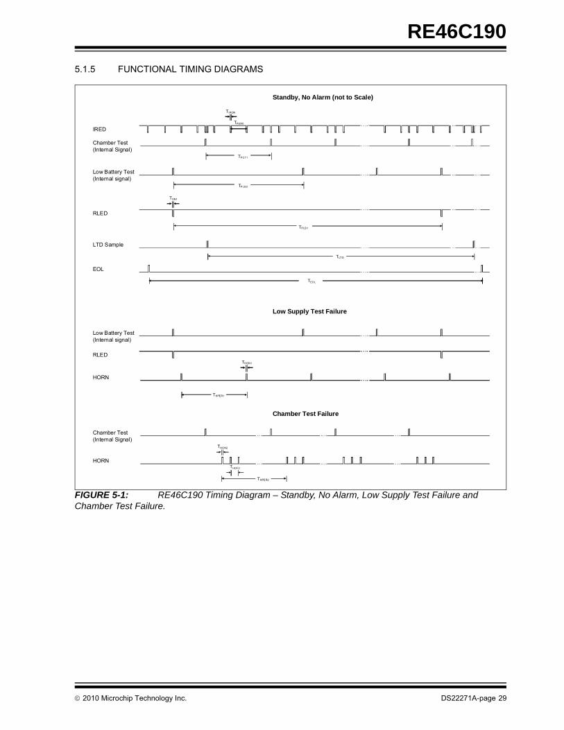
5.1.5 FUNCTIONAL TIMING DIAGRAMS
FIGURE 5-1: RE46C190 Timing Diagram – Standby, No Alarm, Low Supply Test Failure and Chamber Test Failure.
Standby, No Alarm (not to Scale)
TIRON
TPER0
IRED
Chamber Test(Internal Signal)
TPCT1
Low Battery Test(Internal signal)
TPLB2
TON1
RLED
TPLB1
LTD Sample
TLT D
EOL
TEOL
Low Supply Test Failure
Low Battery Test(Internal signal)
RLEDTHON1
HORN
THPER1
Chamber Test Failure
Chamber Test(Internal Signal)
THON2
HORNTHOF2
THPER2
2010 Microchip Technology Inc. DS22271A-page 29

RE46C190
FIGURE 5-2: RE46C190 Timing Diagram – Local Alarm with Temporal Horn Pattern, Local Alarm with International Horn Pattern, Interconnect as Input with Temporal Horn Pattern and Interconnect as Input with International Horn Pattern.
Local Alarm with Temporal Horn Pattern (not to Scale)
No Alarm Local Alarm
TIRON
IRED
TPER3A
TON1
RLED
TPLED2A
THON2A THOF2A THOF3A
HORNTIODLY1
IO as Output
Local Alarm with International Horn Pattern (not to Scale)
No Alarm Local Alarm
TIRON
IRED
TPER3B
TON1
RLED
TPLED2B
THON2B THOF2B
HORN
TIODLY1
IO as Output
Interconnect as Input with Temporal Horn pattern (not to Scale)
TIOFILT
IO as Input
TIODLYA
HORN
Interconnect as Input with International Horn Pattern (not to Scale)
TIOFILT
IO as Input
TIODLYB
DS22271A-page 30 2010 Microchip Technology Inc.

RE46C190
FIGURE 5-3: RE46C190 Timing Diagram – Alarm Memory and Hush Timer.
Alarm Memory (not to Scale)
Alarm Memory
Alarm, No Low Battery Alarm Memory; No Alarm; No Low Battery Alarm Memory After 24 Hour Timer Indication
RLED
TPLED1 TPLED1
TON1 TPLED2
GLED
TON1 TOFLED
TPLED1
TLALED
THON4
HB
THPER4
TEST
Hush Timer (not to Scale)
Alarm, No Low Battery Timer Mode; No Alarm; No Low Battery Standby, No Alarm
RLED
TPLED4 TPLED1
TON1 TPLED2
TTPER
HB
TEST
2010 Microchip Technology Inc. DS22271A-page 31

RE46C190
NOTES:
DS22271A-page 32 2010 Microchip Technology Inc.
RE46C190
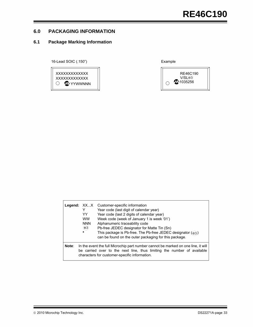
6.0 PACKAGING INFORMATION
6.1 Package Marking Information
Legend: XX...X Customer-specific informationY Year code (last digit of calendar year)YY Year code (last 2 digits of calendar year)WW Week code (week of January 1 is week ‘01’)NNN Alphanumeric traceability code Pb-free JEDEC designator for Matte Tin (Sn)* This package is Pb-free. The Pb-free JEDEC designator ( )
can be found on the outer packaging for this package.
Note: In the event the full Microchip part number cannot be marked on one line, it willbe carried over to the next line, thus limiting the number of availablecharacters for customer-specific information.
3e
3e
16-Lead SOIC (.150”)
XXXXXXXXXXXXXXXXXXXXXXXXXX
YYWWNNN
Example
RE46C190
10352563eV/SL
2010 Microchip Technology Inc. DS22271A-page 33

RE46C190
���������� ��������� ������������������� ��!��"#��$%&
�� ��'�� �������� !�����"�#�$��%!��&������'�(!%�&! %�(�����%�"�)�%����%�����%���"������� *������$����%�+����%�� %���,� ��&�� �� �����"�-��"��%�����!"��&�"�$�� ����%! �� ����"�$�� ����%! �� � ������%��#���"����.�&&���� �"���� ��&�� ��������"�%���������������-�/���.��
0�+1 0� �����&�� ���� ���%��������#��%����!�� �)��)�%�!%�%������ ��-21 ��$��������&�� ��'�! !�����)�%�!%�%������'�$���$&�%����!� � �����
�� �' 2�%���& %��!��%����3����"�)��� '����� �� ���%��������������3�����������$���%������%�"��%��%%�144)))�&��������&4���3�����
5��% ��66��- -����&�� ���6�&�% ��7 78� ��9
7!&(��$���� 7 �:��%�� � �����0�+8������;����% � < < ���.��"�"����3���� ���3�� �� ���. < <�%��"$$��* �� ���� < ���.8������=�"%� - :����0�+��"�"����3����=�"%� -� ,����0�+8������6���%� � �����0�++��&$��>�%����? � ���. < ��.�2%�6���%� 6 ���� < ����2%���% 6� ������-22%������ � �@ < A@6��"� ���3�� � ���� < ���.6��"�=�"%� ( ��,� < ��.���"���$%������� � � .@ < �.@��"���$%�������0%%& � .@ < �.@
D
EE1
N
NOTE 1
1 2 3
b
e
h
h
c
L
L1
A2A
A1 β
φ
α
������� ������� ��)��� +�����A0
DS22271A-page 34 2010 Microchip Technology Inc.

RE46C190
Note: For the most current package drawings, please see the Microchip Packaging Specification located at http://www.microchip.com/packaging
2010 Microchip Technology Inc. DS22271A-page 35

RE46C190
NOTES:
DS22271A-page 36 2010 Microchip Technology Inc.

RE46C190
APPENDIX A: REVISION HISTORY
Revision A (December 2010)
• Original Release of this Document.
2010 Microchip Technology Inc. DS22271A-page 37

RE46C190
NOTES:
DS22271A-page 38 2010 Microchip Technology Inc.

RE46C190
PRODUCT IDENTIFICATION SYSTEM
To order or obtain information, e.g., on pricing or delivery, refer to the factory or the listed sales office.
Device RE46C190: CMOS Photoelectric Smoke Detector ASICRE46C190T: CMOS Photoelectric Smoke Detector ASIC
(Tape and Reel)
Package S = Small Plastic Outline - Narrow, 3.90 mm Body, 16-Lead (SOIC)
Examples:
a) RE46C190S16F: 16LD SOIC Package,Lead Free
b) RE46C190S16TF: 16LD SOIC Package, Tape and Reel, Lead Free
PART NO. X
PackageDevice
XX
Number of Pins
T
Tape and Reel Free
X
Lead
2010 Microchip Technology Inc. DS22271A-page 39

RE46C190
NOTES:
DS22271A-page 40 2010 Microchip Technology Inc.

Note the following details of the code protection feature on Microchip devices:
• Microchip products meet the specification contained in their particular Microchip Data Sheet.
• Microchip believes that its family of products is one of the most secure families of its kind on the market today, when used in the intended manner and under normal conditions.
• There are dishonest and possibly illegal methods used to breach the code protection feature. All of these methods, to our knowledge, require using the Microchip products in a manner outside the operating specifications contained in Microchip’s Data Sheets. Most likely, the person doing so is engaged in theft of intellectual property.
• Microchip is willing to work with the customer who is concerned about the integrity of their code.
• Neither Microchip nor any other semiconductor manufacturer can guarantee the security of their code. Code protection does not mean that we are guaranteeing the product as “unbreakable.”
Code protection is constantly evolving. We at Microchip are committed to continuously improving the code protection features of ourproducts. Attempts to break Microchip’s code protection feature may be a violation of the Digital Millennium Copyright Act. If such actsallow unauthorized access to your software or other copyrighted work, you may have a right to sue for relief under that Act.
Information contained in this publication regarding deviceapplications and the like is provided only for your convenienceand may be superseded by updates. It is your responsibility toensure that your application meets with your specifications.MICROCHIP MAKES NO REPRESENTATIONS ORWARRANTIES OF ANY KIND WHETHER EXPRESS ORIMPLIED, WRITTEN OR ORAL, STATUTORY OROTHERWISE, RELATED TO THE INFORMATION,INCLUDING BUT NOT LIMITED TO ITS CONDITION,QUALITY, PERFORMANCE, MERCHANTABILITY ORFITNESS FOR PURPOSE. Microchip disclaims all liabilityarising from this information and its use. Use of Microchipdevices in life support and/or safety applications is entirely atthe buyer’s risk, and the buyer agrees to defend, indemnify andhold harmless Microchip from any and all damages, claims,suits, or expenses resulting from such use. No licenses areconveyed, implicitly or otherwise, under any Microchipintellectual property rights.
2010 Microchip Technology Inc.
Trademarks
The Microchip name and logo, the Microchip logo, dsPIC, KEELOQ, KEELOQ logo, MPLAB, PIC, PICmicro, PICSTART, PIC32 logo, rfPIC and UNI/O are registered trademarks of Microchip Technology Incorporated in the U.S.A. and other countries.
FilterLab, Hampshire, HI-TECH C, Linear Active Thermistor, MXDEV, MXLAB, SEEVAL and The Embedded Control Solutions Company are registered trademarks of Microchip Technology Incorporated in the U.S.A.
Analog-for-the-Digital Age, Application Maestro, CodeGuard, dsPICDEM, dsPICDEM.net, dsPICworks, dsSPEAK, ECAN, ECONOMONITOR, FanSense, HI-TIDE, In-Circuit Serial Programming, ICSP, Mindi, MiWi, MPASM, MPLAB Certified logo, MPLIB, MPLINK, mTouch, Omniscient Code Generation, PICC, PICC-18, PICDEM, PICDEM.net, PICkit, PICtail, REAL ICE, rfLAB, Select Mode, Total Endurance, TSHARC, UniWinDriver, WiperLock and ZENA are trademarks of Microchip Technology Incorporated in the U.S.A. and other countries.
SQTP is a service mark of Microchip Technology Incorporated in the U.S.A.
All other trademarks mentioned herein are property of their respective companies.
© 2010, Microchip Technology Incorporated, Printed in the U.S.A., All Rights Reserved.
Printed on recycled paper.
ISBN: 978-1-60932-782-8
DS22271A-page 41
Microchip received ISO/TS-16949:2002 certification for its worldwide headquarters, design and wafer fabrication facilities in Chandler and Tempe, Arizona; Gresham, Oregon and design centers in California and India. The Company’s quality system processes and procedures are for its PIC® MCUs and dsPIC® DSCs, KEELOQ® code hopping devices, Serial EEPROMs, microperipherals, nonvolatile memory and analog products. In addition, Microchip’s quality system for the design and manufacture of development systems is ISO 9001:2000 certified.

DS22271A-page 42 2010 Microchip Technology Inc.
AMERICASCorporate Office2355 West Chandler Blvd.Chandler, AZ 85224-6199Tel: 480-792-7200 Fax: 480-792-7277Technical Support: http://support.microchip.comWeb Address: www.microchip.com
AtlantaDuluth, GA Tel: 678-957-9614 Fax: 678-957-1455
BostonWestborough, MA Tel: 774-760-0087 Fax: 774-760-0088
ChicagoItasca, IL Tel: 630-285-0071 Fax: 630-285-0075
ClevelandIndependence, OH Tel: 216-447-0464 Fax: 216-447-0643
DallasAddison, TX Tel: 972-818-7423 Fax: 972-818-2924
DetroitFarmington Hills, MI Tel: 248-538-2250Fax: 248-538-2260
KokomoKokomo, IN Tel: 765-864-8360Fax: 765-864-8387
Los AngelesMission Viejo, CA Tel: 949-462-9523 Fax: 949-462-9608
Santa ClaraSanta Clara, CA Tel: 408-961-6444Fax: 408-961-6445
TorontoMississauga, Ontario, CanadaTel: 905-673-0699 Fax: 905-673-6509
ASIA/PACIFICAsia Pacific OfficeSuites 3707-14, 37th FloorTower 6, The GatewayHarbour City, KowloonHong KongTel: 852-2401-1200Fax: 852-2401-3431
Australia - SydneyTel: 61-2-9868-6733Fax: 61-2-9868-6755
China - BeijingTel: 86-10-8528-2100 Fax: 86-10-8528-2104
China - ChengduTel: 86-28-8665-5511Fax: 86-28-8665-7889
China - ChongqingTel: 86-23-8980-9588Fax: 86-23-8980-9500
China - Hong Kong SARTel: 852-2401-1200 Fax: 852-2401-3431
China - NanjingTel: 86-25-8473-2460Fax: 86-25-8473-2470
China - QingdaoTel: 86-532-8502-7355Fax: 86-532-8502-7205
China - ShanghaiTel: 86-21-5407-5533 Fax: 86-21-5407-5066
China - ShenyangTel: 86-24-2334-2829Fax: 86-24-2334-2393
China - ShenzhenTel: 86-755-8203-2660 Fax: 86-755-8203-1760
China - WuhanTel: 86-27-5980-5300Fax: 86-27-5980-5118
China - XianTel: 86-29-8833-7252Fax: 86-29-8833-7256
China - XiamenTel: 86-592-2388138 Fax: 86-592-2388130
China - ZhuhaiTel: 86-756-3210040 Fax: 86-756-3210049
ASIA/PACIFICIndia - BangaloreTel: 91-80-3090-4444 Fax: 91-80-3090-4123
India - New DelhiTel: 91-11-4160-8631Fax: 91-11-4160-8632
India - PuneTel: 91-20-2566-1512Fax: 91-20-2566-1513
Japan - YokohamaTel: 81-45-471- 6166 Fax: 81-45-471-6122
Korea - DaeguTel: 82-53-744-4301Fax: 82-53-744-4302
Korea - SeoulTel: 82-2-554-7200Fax: 82-2-558-5932 or 82-2-558-5934
Malaysia - Kuala LumpurTel: 60-3-6201-9857Fax: 60-3-6201-9859
Malaysia - PenangTel: 60-4-227-8870Fax: 60-4-227-4068
Philippines - ManilaTel: 63-2-634-9065Fax: 63-2-634-9069
SingaporeTel: 65-6334-8870Fax: 65-6334-8850
Taiwan - Hsin ChuTel: 886-3-6578-300Fax: 886-3-6578-370
Taiwan - KaohsiungTel: 886-7-213-7830Fax: 886-7-330-9305
Taiwan - TaipeiTel: 886-2-2500-6610 Fax: 886-2-2508-0102
Thailand - BangkokTel: 66-2-694-1351Fax: 66-2-694-1350
EUROPEAustria - WelsTel: 43-7242-2244-39Fax: 43-7242-2244-393Denmark - CopenhagenTel: 45-4450-2828 Fax: 45-4485-2829
France - ParisTel: 33-1-69-53-63-20 Fax: 33-1-69-30-90-79
Germany - MunichTel: 49-89-627-144-0 Fax: 49-89-627-144-44
Italy - Milan Tel: 39-0331-742611 Fax: 39-0331-466781
Netherlands - DrunenTel: 31-416-690399 Fax: 31-416-690340
Spain - MadridTel: 34-91-708-08-90Fax: 34-91-708-08-91
UK - WokinghamTel: 44-118-921-5869Fax: 44-118-921-5820
Worldwide Sales and Service
08/04/10