mcp87130 data sheet - microchip technologyww1.microchip.com/downloads/en/devicedoc/20005159b.pdf ·...
TRANSCRIPT

MCP87130High-Speed N-Channel Power MOSFET
Features:• Low Drain-to-Source On Resistance (RDS(ON))• Low Total Gate Charge (QG) and Gate-to-Drain
Charge (QGD)• Low Series Gate Resistance (RG)• Capable of Short Dead-Time Operation• RoHS Compliant
Applications:• Point-of-Load DC-DC Converters• High Efficiency Power Management in Servers,
Networking, and Automotive Applications
Description:
The MCP87130 is an N-Channel power MOSFET in apopular PDFN 5 mm x 6 mm package as well as aPDFN 3.3 mm x 3.3 mm package. Advancedpackaging and silicon processing technologies allowthe MCP87130 to achieve a low QG for a given RDS(ON)value, resulting in a low Figure of Merit (FOM).Combined with low RG, the low FOM of the MCP87130allows high efficiency power conversion with reducedswitching and conduction losses.
Package Type
S
G
S
S
D
D
D
D
1
2
3
4 5
6
7
8PDFN 5 x 6 PDFN 3.3 x 3.3
Product Summary Table: Unless otherwise indicated, TA = +25˚C.
Parameters Sym. Min. Typ. Max. Units Conditions
Operating Characteristics
Drain-to-Source Breakdown Voltage BVDSS 25 — — V VGS = 0V, ID = 250 µA
Gate-to-Source Threshold Voltage VGS(TH) 1.1 1.35 1.7 V VDS = VGS, ID = 250 µA
Drain-to-Source On Resistance RDS(ON) — 13.8 16.5 mΩ VGS = 4.5V, ID = 10A
— 11.3 13.5 mΩ VGS = 10V, ID = 10A
Total Gate Charge QG — 5.5 8 nC VDS = 12.5V, ID = 10A, VGS = 4.5V
Gate-to-Drain Charge QGD — 2.6 — nC VDS = 12.5V, ID = 10A
Series Gate Resistance RG — 1.7 — Ω
Thermal Characteristics
Thermal Resistance Junction-to-X, 8L 3.3x3.3-PDFN RθJX — — 73 °C/W Note 1
Thermal Resistance Junction-to-Case, 8L 3.3x3.3-PDFN RθJC — — 3.3 °C/W Note 2
Thermal Resistance Junction-to-X, 8L 5x6-PDFN RθJX — — 58 °C/W Note 1
Thermal Resistance Junction-to-Case, 8L 5x6-PDFN RθJC — — 3.3 °C/W Note 2
Note 1: RθJX is determined with the device surface mounted on a 4-Layer FR4 PCB, with a 1” x 1” mounting pad of 2 oz. cop-per. This characteristic is dependent on user’s board design.
2: RθJC is determined using JEDEC 51-14 Method. This characteristic is determined by design.
2013 Microchip Technology Inc. DS20005159B-page 1
MCP87130
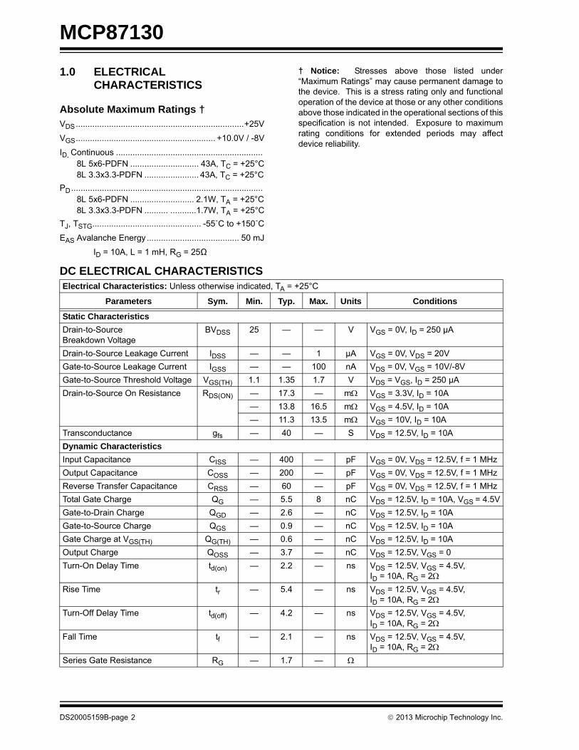
1.0 ELECTRICAL CHARACTERISTICS
Absolute Maximum Ratings †VDS.......................................................................+25V
VGS........................................................... +10.0V / -8V
ID, Continuous ..............................................................8L 5x6-PDFN ............................. 43A, TC = +25°C8L 3.3x3.3-PDFN ....................... 43A, TC = +25°C
PD.................................................................................8L 5x6-PDFN ........................... 2.1W, TA = +25°C8L 3.3x3.3-PDFN .......... ...........1.7W, TA = +25°C
TJ, TSTG.............................................. -55˚C to +150˚C
EAS Avalanche Energy ....................................... 50 mJ
ID = 10A, L = 1 mH, RG = 25Ω
† Notice: Stresses above those listed under“Maximum Ratings” may cause permanent damage tothe device. This is a stress rating only and functionaloperation of the device at those or any other conditionsabove those indicated in the operational sections of thisspecification is not intended. Exposure to maximumrating conditions for extended periods may affectdevice reliability.
DC ELECTRICAL CHARACTERISTICSElectrical Characteristics: Unless otherwise indicated, TA = +25°C
Parameters Sym. Min. Typ. Max. Units Conditions
Static Characteristics
Drain-to-Source Breakdown Voltage
BVDSS 25 — — V VGS = 0V, ID = 250 µA
Drain-to-Source Leakage Current IDSS — — 1 µA VGS = 0V, VDS = 20V
Gate-to-Source Leakage Current IGSS — — 100 nA VDS = 0V, VGS = 10V/-8V
Gate-to-Source Threshold Voltage VGS(TH) 1.1 1.35 1.7 V VDS = VGS, ID = 250 µA
Drain-to-Source On Resistance RDS(ON) — 17.3 — m VGS = 3.3V, ID = 10A
— 13.8 16.5 m VGS = 4.5V, ID = 10A
— 11.3 13.5 m VGS = 10V, ID = 10A
Transconductance gfs — 40 — S VDS = 12.5V, ID = 10A
Dynamic Characteristics
Input Capacitance CISS — 400 — pF VGS = 0V, VDS = 12.5V, f = 1 MHz
Output Capacitance COSS — 200 — pF VGS = 0V, VDS = 12.5V, f = 1 MHz
Reverse Transfer Capacitance CRSS — 60 — pF VGS = 0V, VDS = 12.5V, f = 1 MHz
Total Gate Charge QG — 5.5 8 nC VDS = 12.5V, ID = 10A, VGS = 4.5V
Gate-to-Drain Charge QGD — 2.6 — nC VDS = 12.5V, ID = 10A
Gate-to-Source Charge QGS — 0.9 — nC VDS = 12.5V, ID = 10A
Gate Charge at VGS(TH) QG(TH) — 0.6 — nC VDS = 12.5V, ID = 10A
Output Charge QOSS — 3.7 — nC VDS = 12.5V, VGS = 0
Turn-On Delay Time td(on) — 2.2 — ns VDS = 12.5V, VGS = 4.5V, ID = 10A, RG = 2
Rise Time tr — 5.4 — ns VDS = 12.5V, VGS = 4.5V, ID = 10A, RG = 2
Turn-Off Delay Time td(off) — 4.2 — ns VDS = 12.5V, VGS = 4.5V, ID = 10A, RG = 2
Fall Time tf — 2.1 — ns VDS = 12.5V, VGS = 4.5V, ID = 10A, RG = 2
Series Gate Resistance RG — 1.7 —
DS20005159B-page 2 2013 Microchip Technology Inc.

MCP87130
Diode Characteristics
Diode Forward Voltage VFD — 0.8 1 V IS = 10A, VGS = 0V
Reverse Recovery Charge QRR — 7 — nC IS = 10A, di/dt = 300 A/µs
Reverse Recovery Time trr — 9.5 — nS IS = 10A, di/dt = 300 A/µs
Avalanche Characteristics
Avalanche Energy EAS 4.5 — — mJ ID = 3A, L = 1 mH, RG = 25
TEMPERATURE CHARACTERISTICSElectrical Characteristics: Unless otherwise indicated, TA = +25°C
Parameters Sym. Min. Typ. Max. Units Conditions
Temperature Ranges
Operating Junction Temperature Range TJ -55 — 150 °C
Storage Temperature Range TA -55 — 150 °C
Package Thermal Resistances
Thermal Resistance Junction-to-X, 8L 3.3x3.3-PDFN RθJX — — 73 °C/W Note 1
Thermal Resistance Junction-to-Case, 8L 3.3x3.3-PDFN
RθJC — — 3.3 °C/W Note 2
Thermal Resistance Junction-to-X, 8L 5x6-PDFN RθJX — — 58 °C/W Note 1
Thermal Resistance Junction-to-Case, 8L 5x6-PDFN RθJC — — 3.3 °C/W Note 2
Note 1: RθJX is determined with the device surface mounted on a 4-Layer FR4 PCB, with a 1” x 1” mounting pad of 2 oz. copper. This characteristic is dependent on user’s board design.
2: RθJC is determined using JEDEC 51-14 Method. This characteristic is determined by design.
DC ELECTRICAL CHARACTERISTICS (CONTINUED)Electrical Characteristics: Unless otherwise indicated, TA = +25°C
Parameters Sym. Min. Typ. Max. Units Conditions
2013 Microchip Technology Inc. DS20005159B-page 3
MCP87130
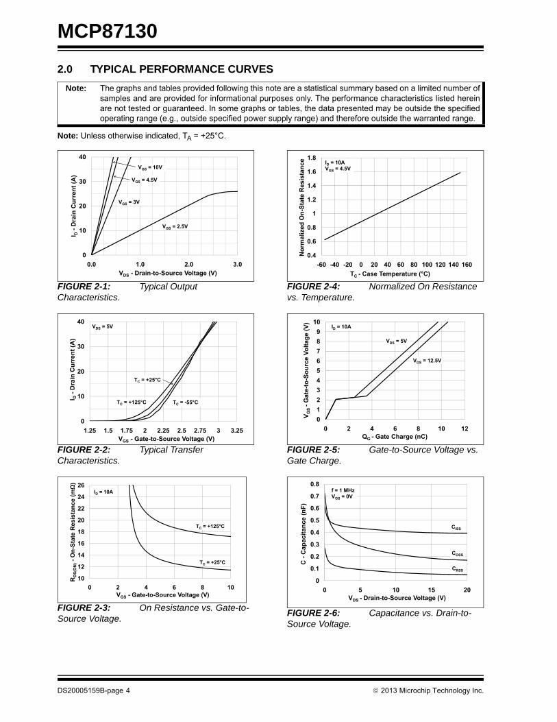
2.0 TYPICAL PERFORMANCE CURVES
Note: Unless otherwise indicated, TA = +25°C.
FIGURE 2-1: Typical Output Characteristics.
FIGURE 2-2: Typical Transfer Characteristics.
FIGURE 2-3: On Resistance vs. Gate-to-Source Voltage.
FIGURE 2-4: Normalized On Resistance vs. Temperature.
FIGURE 2-5: Gate-to-Source Voltage vs. Gate Charge.
FIGURE 2-6: Capacitance vs. Drain-to-Source Voltage.
Note: The graphs and tables provided following this note are a statistical summary based on a limited number ofsamples and are provided for informational purposes only. The performance characteristics listed hereinare not tested or guaranteed. In some graphs or tables, the data presented may be outside the specifiedoperating range (e.g., outside specified power supply range) and therefore outside the warranted range.
20
30
40
Dra
in C
urre
nt (A
)
VGS = 3V
VGS = 10V
VGS = 4.5V
0
10
0.0 1.0 2.0 3.0
I D-D
VDS - Drain-to-Source Voltage (V)
VGS = 2.5V
20
30
40
Dra
in C
urre
nt (A
)
TC = +25°C
VDS = 5V
0
10
1.25 1.5 1.75 2 2.25 2.5 2.75 3 3.25
I D-D
VGS - Gate-to-Source Voltage (V)
TC = +125°C TC = -55°C
16
18
20
22
24
26
Stat
e R
esis
tanc
e (m
)
TC = +125°C
ID = 10A
10
12
14
0 2 4 6 8 10
RD
S(O
N)-O
n-S
VGS - Gate-to-Source Voltage (V)
TC = +25°C
1
1.2
1.4
1.6
1.8
d O
n-St
ate
Res
ista
nce ID = 10A
VGS = 4.5V
0.4
0.6
0.8
-60 -40 -20 0 20 40 60 80 100 120 140 160
Nor
mal
ized
TC - Case Temperature (°C)
456789
10
-to-S
ourc
e Vo
ltage
(V)
ID = 10A
VDS = 5V
VDS = 12.5V
0123
0 2 4 6 8 10 12
V GS
-Gat
e-
QG - Gate Charge (nC)
0.3
0.4
0.5
0.6
0.7
0.8
apac
itanc
e (n
F)
CISS
f = 1 MHzVGS = 0V
0
0.1
0.2
0 5 10 15 20
C -
Ca
VDS - Drain-to-Source Voltage (V)
COSS
CRSS
DS20005159B-page 4 2013 Microchip Technology Inc.

MCP87130
Note: Unless otherwise indicated, TA = +25°C.
FIGURE 2-7: Gate-to-Source Threshold Voltage vs. Temperature.
FIGURE 2-8: Source-to-Drain Current vs. Source-to-Drain Voltage.
FIGURE 2-9: Maximum Safe Operating Area 5x6-PDFN (MCP87130T-U/MF).
FIGURE 2-10: Maximum Drain Current vs. Temperature 5x6-PDFN (MCP87130T-U/MF).
FIGURE 2-11: Transient Thermal Impedance 5x6-PDFN (MCP87130T-U/MF).
FIGURE 2-12: Maximum Safe Operating Area 3.3x3.3-PDFN (MCP87130T-U/LC).
1.3
1.5
1.7te
-to-S
ourc
e Th
resh
old
Volta
ge (V
)ID = 250 μA
0.9
1.1
-75 -50 -25 0 25 50 75 100 125 150 175
V GS(
TH) -
Gat
TC - Case Temperature (°C)
0.1
1
10
100
ce-to
-Dra
in C
urre
nt (A
)
TC = +25°CTC = +125°C
0.001
0.01
0.0 0.2 0.4 0.6 0.8 1.0
I SD
-Sou
rc
VSD - Source-to-Drain Voltage (V)
0.01
0.1
1
10
100
1000
0.01 0.1 1 10 100
I D-D
rain
Cur
rent
(A)
VDS - Drain-to-Source Voltage (V)
DC
1s100 ms
10 ms
1 ms
Operation in this range is limited by RDS(on)
R JA = 58 °C/WSingle Pulse
0
10
20
30
40
50
60
70
0 25 50 75 100 125 150
I D-D
rain
Cur
rent
(A)
TC - Case Temperature (
VGS = 4.5V
VGS = 10V
0.001
0.01
0.1
1
0.001 0.1 10 1000
ZJA
-Nor
mal
ized
The
rmal
Im
peda
nce
t1 - Pulse Duration (s)
DC = 0.5DC = 0.3DC = 0.1DC = 0.05DC = 0.02DC = 0.01Single Pulse
0.01
0.1
1
10
100
1000
0.01 0.1 1 10 100
I D-D
rain
Cur
rent
(A)
VDS - Drain-to-Source Voltage (V)
DC1s
100 ms10 ms
1 ms
Operation in this range is limited by RDS(on)
R JA = 73 °C/WSingle Pulse
2013 Microchip Technology Inc. DS20005159B-page 5

MCP87130
FIGURE 2-13: Maximum Drain Current vs. Temperature 3.3x3.3-PDFN (MCP87130T-U/LC).
FIGURE 2-14: Transient Thermal Impedance 3.3x3.3-PDFN (MCP87130T-U/LC).
FIGURE 2-15: Single-Pulse Unclamped Inductive Switching.
FIGURE 2-16: Drain-to-Source Breakdown Voltage vs. Temperature.
0
10
20
30
40
50
60
70
0 25 50 75 100 125 150
I D-D
rain
Cur
rent
(A)
TC - Case Temperature (
VGS = 4.5V
VGS = 10V
0.001
0.01
0.1
1
0.001 0.1 10 1000
ZJA
-Nor
mal
ized
The
rmal
Im
peda
nce
t1 - Pulse Duration (s)
DC = 0.5DC = 0.3DC = 0.1DC = 0.05DC = 0.02DC = 0.01Single Pulse
10
alan
che
Cur
rent
(A)
TC = +25°C
TC = +150°C
10.01 0.1 1 10
I AS
-Ava
tAV - Avalanche Time (ms)
27
28
29
30
31
Bre
akdo
wn
Volta
ge (V
)
ID = 250 μA
25
26
-60 -40 -20 0 20 40 60 80 100 120 140 160
V BR
(DSS
)-B
TC - Case Temperature(°C)
DS20005159B-page 6 2013 Microchip Technology Inc.

MCP87130
3.0 PIN DESCRIPTIONS
The descriptions of the pins are listed in Table 3-1.
TABLE 3-1: PINOUT DESCRIPTION FOR THE MCP87130
MCP87130
Pin Type Function5x6 PDFN, 3.3 x 3.3 PDFN
1, 2, 3 S Source pin
4 G Gate pin
5, 6, 7, 8 D Drain pin, including exposed thermal pad
2013 Microchip Technology Inc. DS20005159B-page 7

MCP87130
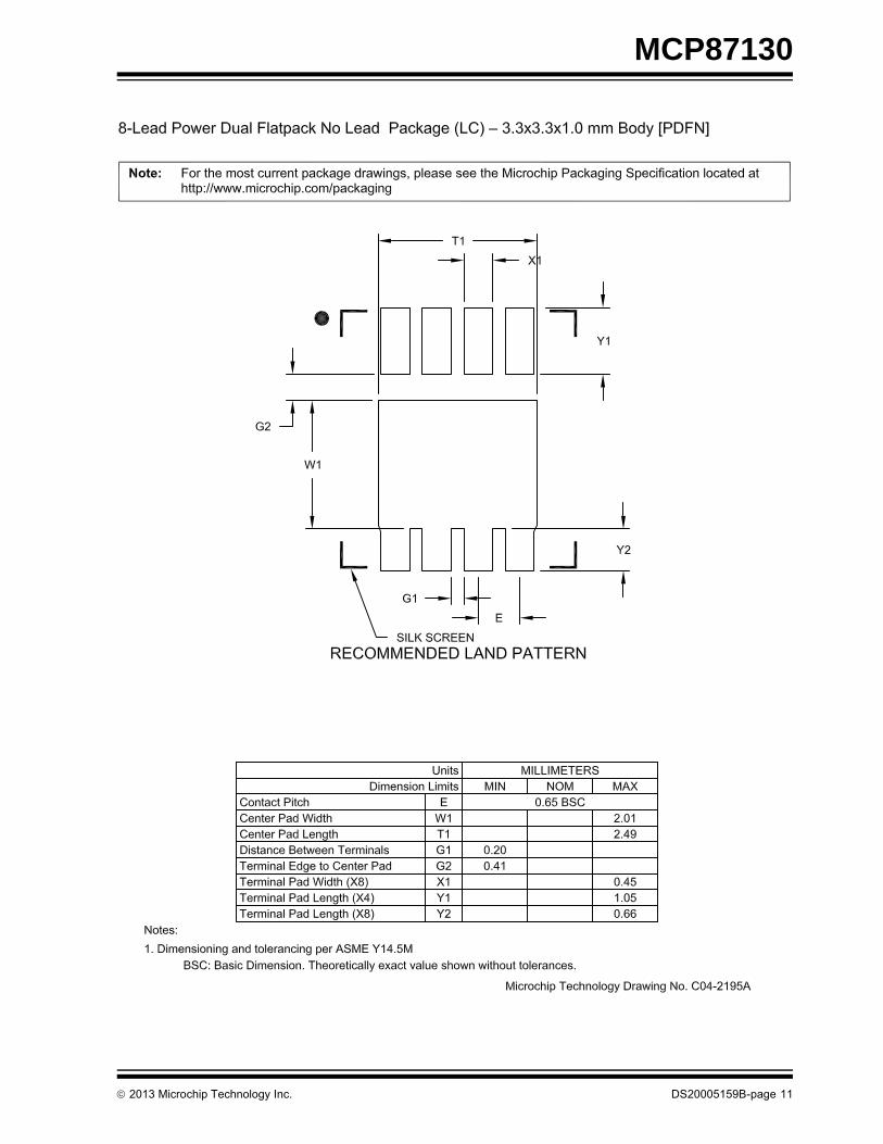
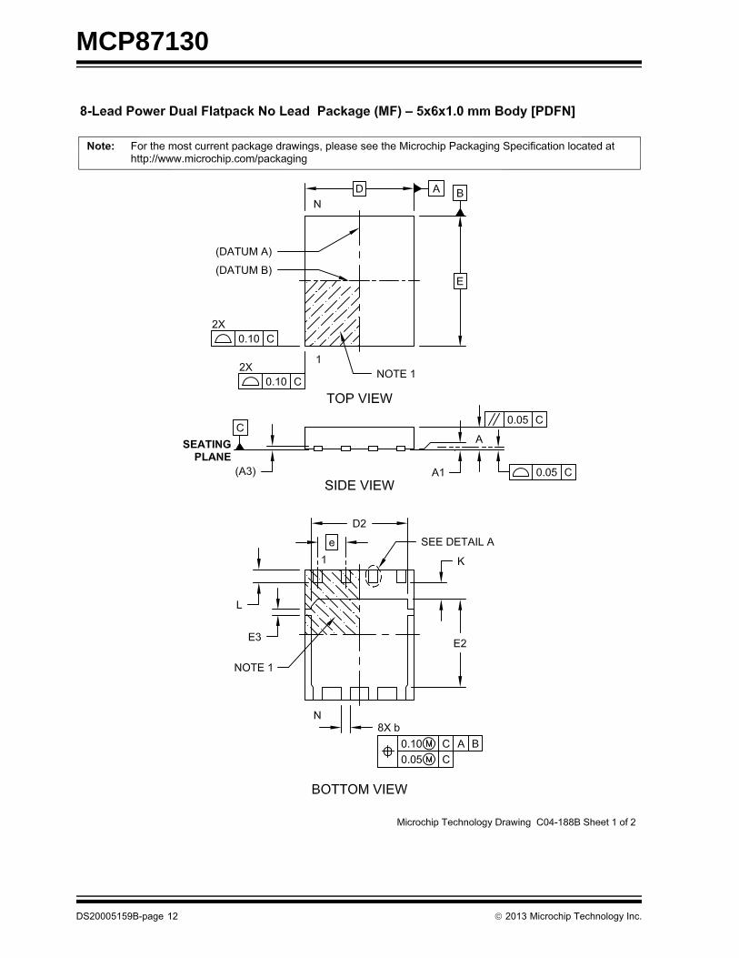
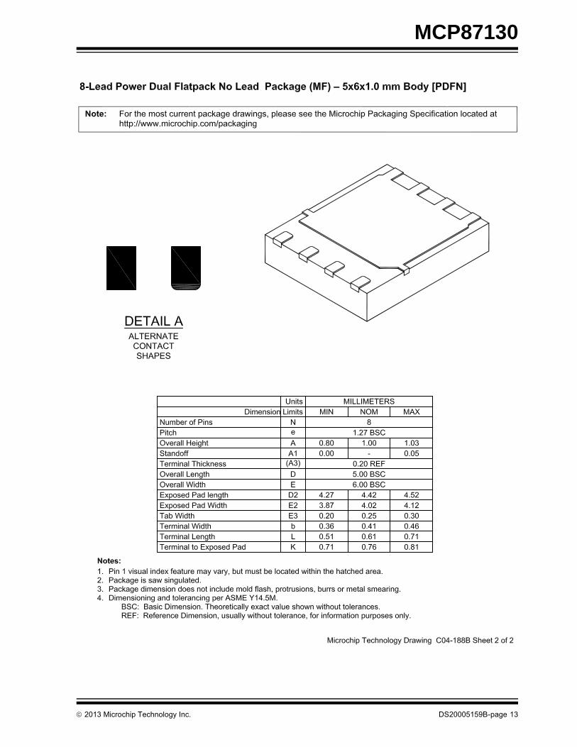
4.0 PACKAGING INFORMATION
4.1 Package Marking Information*
PIN 1
NNN
PIN 1
8-Lead PDFN (5x6x1.0 mm) Example
Note: In the event the full Microchip part number cannot be marked on one line, it willbe carried over to the next line, thus limiting the number of availablecharacters for customer-specific information.
*RoHS compliant using EU-RoHS exemption: 7(a) - Lead in high-melting-temperature-type solders(i.e. lead-based alloys containing 85% by weight or more lead) can be found on the outerpackaging for this package.
Legend: XX...X Customer-specific informationY Year code (last digit of calendar year)YY Year code (last 2 digits of calendar year)WW Week code (week of January 1 is week ‘01’)NNN Alphanumeric traceability code Pb-free JEDEC designator for Matte Tin (Sn)* This package is Pb-free. The Pb-free JEDEC designator ( )
can be found on the outer packaging for this package.3e
87130U/MF ^^
1236256
3e
3e
130U1236256
8-Lead PDFN (3.3x3.3x1.0 mm) Example
DS20005159B-page 8 2013 Microchip Technology Inc.

MCP87130
2013 Microchip Technology Inc. DS20005159B-page 9

MCP87130
DS20005159B-page 10 2013 Microchip Technology Inc.
MCP87130
2013 Microchip Technology Inc. DS20005159B-page 11
MCP87130
DS20005159B-page 12 2013 Microchip Technology Inc.
MCP87130
2013 Microchip Technology Inc. DS20005159B-page 13

MCP87130
DS20005159B-page 14 2013 Microchip Technology Inc.

2013 Microchip Technology Inc. DS20005159B-page 15
MCP87130
APPENDIX A: REVISION HISTORY
Revision B (August 2013)
The following is the list of modifications.
1. Updated the Thermal Resistances maximumvalues in the Temperature Characteristics table.
2. Added Figure 2-9, Figure 2-10, Figure 2-11,Figure 2-12, Figure 2-13 and Figure 2-14.
Revision A (January 2013)
• Original Release of this Document.

MCP87130
DS20005159B-page 16 2013 Microchip Technology Inc.
PRODUCT IDENTIFICATION SYSTEM
To order or obtain information, e.g., on pricing or delivery, refer to the factory or the listed sales office.
PART NO. X /XX
PackageTemperatureRange
Device
Device: MCP87130T: N-Channel power MOSFET (Tape and Reel) (PDFN)
Temperature Range: U = -55°C to +150°C (Ultra High)
Package: LC = High-Power Dual Flatpack, No Lead Package (3.3x3.3x1.0 mm Body) (PDFN), 8-lead
MF = High-Power Dual Flatpack, No Lead Package (5x6x1.0 mm Body) (PDFN), 8-lead
Example:
a) MCP87130T-U/LC: Tape and Reel, Ultra-High Temperature, 8LD 3.3x3.3 PDFN package
b) MCP87130T-U/MF: Tape and Reel, Ultra-High Temperature, 8LD 5x6 PDFN package
Note the following details of the code protection feature on Microchip devices:
• Microchip products meet the specification contained in their particular Microchip Data Sheet.
• Microchip believes that its family of products is one of the most secure families of its kind on the market today, when used in the intended manner and under normal conditions.
• There are dishonest and possibly illegal methods used to breach the code protection feature. All of these methods, to our knowledge, require using the Microchip products in a manner outside the operating specifications contained in Microchip’s Data Sheets. Most likely, the person doing so is engaged in theft of intellectual property.
• Microchip is willing to work with the customer who is concerned about the integrity of their code.
• Neither Microchip nor any other semiconductor manufacturer can guarantee the security of their code. Code protection does not mean that we are guaranteeing the product as “unbreakable.”
Code protection is constantly evolving. We at Microchip are committed to continuously improving the code protection features of ourproducts. Attempts to break Microchip’s code protection feature may be a violation of the Digital Millennium Copyright Act. If such actsallow unauthorized access to your software or other copyrighted work, you may have a right to sue for relief under that Act.
Information contained in this publication regarding deviceapplications and the like is provided only for your convenienceand may be superseded by updates. It is your responsibility toensure that your application meets with your specifications.MICROCHIP MAKES NO REPRESENTATIONS ORWARRANTIES OF ANY KIND WHETHER EXPRESS ORIMPLIED, WRITTEN OR ORAL, STATUTORY OROTHERWISE, RELATED TO THE INFORMATION,INCLUDING BUT NOT LIMITED TO ITS CONDITION,QUALITY, PERFORMANCE, MERCHANTABILITY ORFITNESS FOR PURPOSE. Microchip disclaims all liabilityarising from this information and its use. Use of Microchipdevices in life support and/or safety applications is entirely atthe buyer’s risk, and the buyer agrees to defend, indemnify andhold harmless Microchip from any and all damages, claims,suits, or expenses resulting from such use. No licenses areconveyed, implicitly or otherwise, under any Microchipintellectual property rights.
2013 Microchip Technology Inc.
QUALITY MANAGEMENT SYSTEM CERTIFIED BY DNV
== ISO/TS 16949 ==
Trademarks
The Microchip name and logo, the Microchip logo, dsPIC, FlashFlex, KEELOQ, KEELOQ logo, MPLAB, PIC, PICmicro, PICSTART, PIC32 logo, rfPIC, SST, SST Logo, SuperFlash and UNI/O are registered trademarks of Microchip Technology Incorporated in the U.S.A. and other countries.
FilterLab, Hampshire, HI-TECH C, Linear Active Thermistor, MTP, SEEVAL and The Embedded Control Solutions Company are registered trademarks of Microchip Technology Incorporated in the U.S.A.
Silicon Storage Technology is a registered trademark of Microchip Technology Inc. in other countries.
Analog-for-the-Digital Age, Application Maestro, BodyCom, chipKIT, chipKIT logo, CodeGuard, dsPICDEM, dsPICDEM.net, dsPICworks, dsSPEAK, ECAN, ECONOMONITOR, FanSense, HI-TIDE, In-Circuit Serial Programming, ICSP, Mindi, MiWi, MPASM, MPF, MPLAB Certified logo, MPLIB, MPLINK, mTouch, Omniscient Code Generation, PICC, PICC-18, PICDEM, PICDEM.net, PICkit, PICtail, REAL ICE, rfLAB, Select Mode, SQI, Serial Quad I/O, Total Endurance, TSHARC, UniWinDriver, WiperLock, ZENA and Z-Scale are trademarks of Microchip Technology Incorporated in the U.S.A. and other countries.
SQTP is a service mark of Microchip Technology Incorporated in the U.S.A.
GestIC and ULPP are registered trademarks of Microchip Technology Germany II GmbH & Co. KG, a subsidiary of Microchip Technology Inc., in other countries.
All other trademarks mentioned herein are property of their respective companies.
© 2013, Microchip Technology Incorporated, Printed in the U.S.A., All Rights Reserved.
Printed on recycled paper.
ISBN: 978-1-62077-423-6
Microchip received ISO/TS-16949:2009 certification for its worldwide
DS20005159B-page 17
headquarters, design and wafer fabrication facilities in Chandler and Tempe, Arizona; Gresham, Oregon and design centers in California and India. The Company’s quality system processes and procedures are for its PIC® MCUs and dsPIC® DSCs, KEELOQ® code hopping devices, Serial EEPROMs, microperipherals, nonvolatile memory and analog products. In addition, Microchip’s quality system for the design and manufacture of development systems is ISO 9001:2000 certified.
DS20005159B-page 18 2013 Microchip Technology Inc.
AMERICASCorporate Office2355 West Chandler Blvd.Chandler, AZ 85224-6199Tel: 480-792-7200 Fax: 480-792-7277Technical Support: http://www.microchip.com/supportWeb Address: www.microchip.com
AtlantaDuluth, GA Tel: 678-957-9614 Fax: 678-957-1455
BostonWestborough, MA Tel: 774-760-0087 Fax: 774-760-0088
ChicagoItasca, IL Tel: 630-285-0071 Fax: 630-285-0075
ClevelandIndependence, OH Tel: 216-447-0464 Fax: 216-447-0643
DallasAddison, TX Tel: 972-818-7423 Fax: 972-818-2924
DetroitFarmington Hills, MI Tel: 248-538-2250Fax: 248-538-2260
IndianapolisNoblesville, IN Tel: 317-773-8323Fax: 317-773-5453
Los AngelesMission Viejo, CA Tel: 949-462-9523 Fax: 949-462-9608
Santa ClaraSanta Clara, CA Tel: 408-961-6444Fax: 408-961-6445
TorontoMississauga, Ontario, CanadaTel: 905-673-0699 Fax: 905-673-6509
ASIA/PACIFICAsia Pacific OfficeSuites 3707-14, 37th FloorTower 6, The GatewayHarbour City, KowloonHong KongTel: 852-2401-1200Fax: 852-2401-3431
Australia - SydneyTel: 61-2-9868-6733Fax: 61-2-9868-6755
China - BeijingTel: 86-10-8569-7000 Fax: 86-10-8528-2104
China - ChengduTel: 86-28-8665-5511Fax: 86-28-8665-7889
China - ChongqingTel: 86-23-8980-9588Fax: 86-23-8980-9500
China - HangzhouTel: 86-571-2819-3187 Fax: 86-571-2819-3189
China - Hong Kong SARTel: 852-2943-5100 Fax: 852-2401-3431
China - NanjingTel: 86-25-8473-2460Fax: 86-25-8473-2470
China - QingdaoTel: 86-532-8502-7355Fax: 86-532-8502-7205
China - ShanghaiTel: 86-21-5407-5533 Fax: 86-21-5407-5066
China - ShenyangTel: 86-24-2334-2829Fax: 86-24-2334-2393
China - ShenzhenTel: 86-755-8864-2200 Fax: 86-755-8203-1760
China - WuhanTel: 86-27-5980-5300Fax: 86-27-5980-5118
China - XianTel: 86-29-8833-7252Fax: 86-29-8833-7256
China - XiamenTel: 86-592-2388138 Fax: 86-592-2388130
China - ZhuhaiTel: 86-756-3210040 Fax: 86-756-3210049
ASIA/PACIFICIndia - BangaloreTel: 91-80-3090-4444 Fax: 91-80-3090-4123
India - New DelhiTel: 91-11-4160-8631Fax: 91-11-4160-8632
India - PuneTel: 91-20-2566-1512Fax: 91-20-2566-1513
Japan - OsakaTel: 81-6-6152-7160 Fax: 81-6-6152-9310
Japan - TokyoTel: 81-3-6880- 3770 Fax: 81-3-6880-3771
Korea - DaeguTel: 82-53-744-4301Fax: 82-53-744-4302
Korea - SeoulTel: 82-2-554-7200Fax: 82-2-558-5932 or 82-2-558-5934
Malaysia - Kuala LumpurTel: 60-3-6201-9857Fax: 60-3-6201-9859
Malaysia - PenangTel: 60-4-227-8870Fax: 60-4-227-4068
Philippines - ManilaTel: 63-2-634-9065Fax: 63-2-634-9069
SingaporeTel: 65-6334-8870Fax: 65-6334-8850
Taiwan - Hsin ChuTel: 886-3-5778-366Fax: 886-3-5770-955
Taiwan - KaohsiungTel: 886-7-213-7828Fax: 886-7-330-9305
Taiwan - TaipeiTel: 886-2-2508-8600 Fax: 886-2-2508-0102
Thailand - BangkokTel: 66-2-694-1351Fax: 66-2-694-1350
EUROPEAustria - WelsTel: 43-7242-2244-39Fax: 43-7242-2244-393Denmark - CopenhagenTel: 45-4450-2828 Fax: 45-4485-2829
France - ParisTel: 33-1-69-53-63-20 Fax: 33-1-69-30-90-79
Germany - MunichTel: 49-89-627-144-0 Fax: 49-89-627-144-44
Italy - Milan Tel: 39-0331-742611 Fax: 39-0331-466781
Netherlands - DrunenTel: 31-416-690399 Fax: 31-416-690340
Spain - MadridTel: 34-91-708-08-90Fax: 34-91-708-08-91
UK - WokinghamTel: 44-118-921-5869Fax: 44-118-921-5820
Worldwide Sales and Service
11/29/12