ray pengelly, cree rf and microwave products, research ... · ray pengelly, cree rf and microwave...
TRANSCRIPT

Ray Pengelly,
Cree RF and Microwave Products,
Research Triangle Park, NC 27709
October 21, 2010
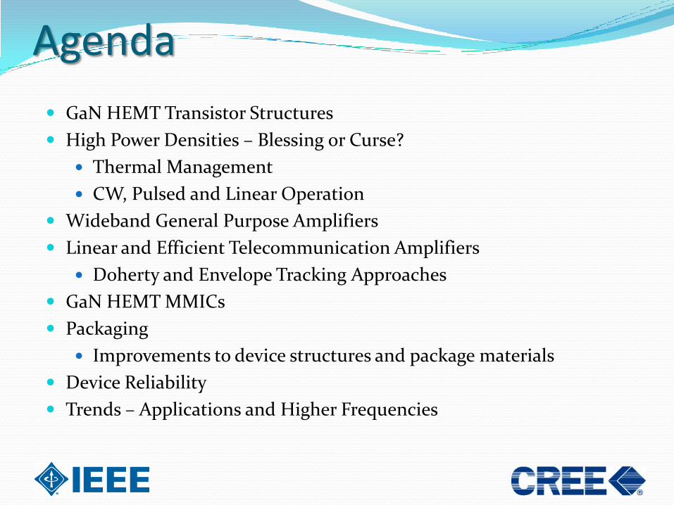
Agenda
GaN HEMT Transistor Structures
High Power Densities – Blessing or Curse?
Thermal Management
CW, Pulsed and Linear Operation
Wideband General Purpose Amplifiers
Linear and Efficient Telecommunication Amplifiers
Doherty and Envelope Tracking Approaches
GaN HEMT MMICs
Packaging
Improvements to device structures and package materials
Device Reliability
Trends – Applications and Higher Frequencies

Strengths of GaN HEMTs High breakdown voltage VDD large; RL high – easier to match; lower losses
High sheet charge density; ns = 1 x 10¹³
Current density is large
Device area can be reduced
Large Watts/mm of gate periphery
High saturated drift velocity High saturation current density and W/mm
Small device area per watt – lower capacitances
Low drain-source capacitance Easier to match
More suitable for switch-mode amplifiers
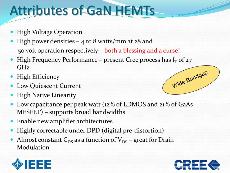
Attributes of GaN HEMTs
High Voltage Operation
High power densities – 4 to 8 watts/mm at 28 and
50 volt operation respectively – both a blessing and a curse!
High Frequency Performance – present Cree process has fT of 27 GHz
High Efficiency
Low Quiescent Current
High Native Linearity
Low capacitance per peak watt (12% of LDMOS and 21% of GaAs MESFET) – supports broad bandwidths
Enable new amplifier architectures
Highly correctable under DPD (digital pre-distortion)
Almost constant CDS as a function of VDS – great for Drain Modulation
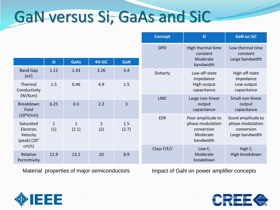
Si GaAs 4H-SiC GaN
Band Gap (eV)
1.12 1.43 3.26 3.4
Thermal Conductivity
(W/Kcm)
1.5 0.46 4.9 1.5
Breakdown Field
(106V/cm)
0.25 0.3 2.2 3
SaturatedElectron Velocity
(peak) (107
cm/s)
1(1)
1(2.1)
2(2)
1.5(2.7)
Relative Permittivity
11.9 13.1 10 8.9
5
GaN versus Si, GaAs and SiCConcept Si GaN on SiC
DPD High thermal time constant
Moderate bandwidth
Low thermal time constant
Large bandwidth
Doherty Low off-state impedanceHigh output capacitance
High off-state impedanceLow output capacitance
LINC Large non-linear output
capacitance
Small non-linear output
capacitance
EER Poor amplitude to phase modulation
conversionModerate bandwidth
Good amplitude to phase modulation
conversionLarge bandwidth
Class F/E/J Low fT
Moderate breakdown
High fT
High breakdown
Impact of GaN on power amplifier conceptsMaterial properties of major semiconductors
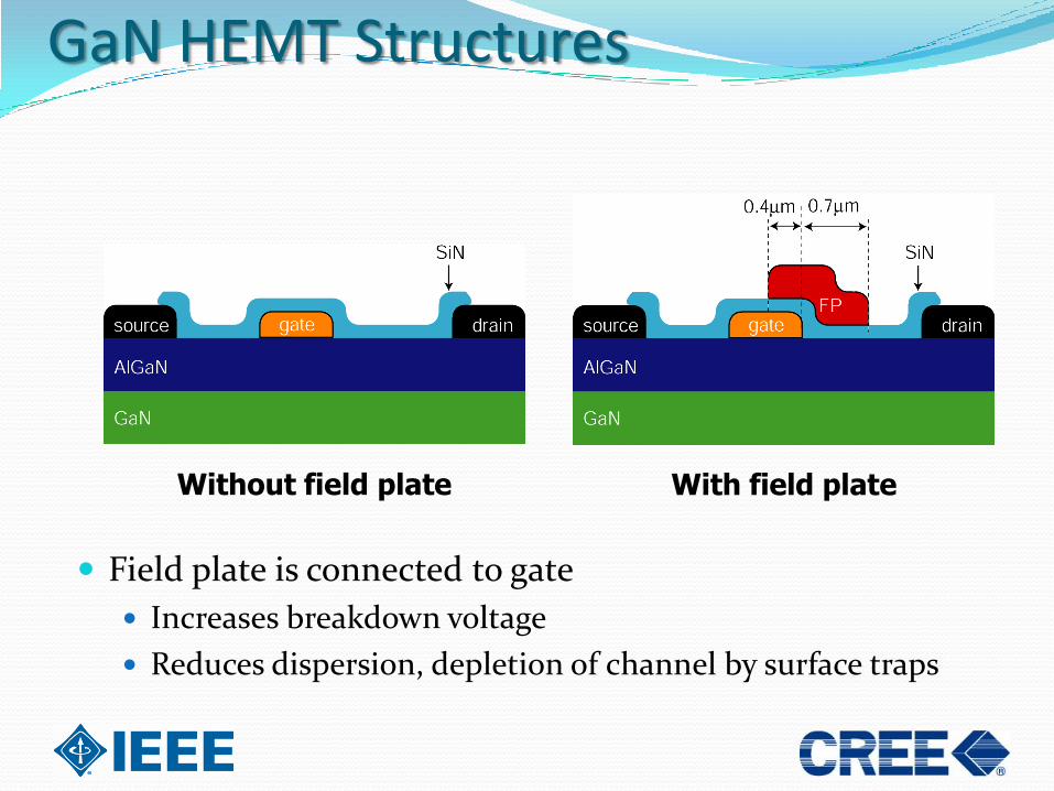
GaN HEMT Structures
Field plate is connected to gate
Increases breakdown voltage
Reduces dispersion, depletion of channel by surface traps
Without field plate With field plate
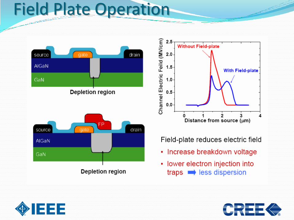
Field Plate Operation
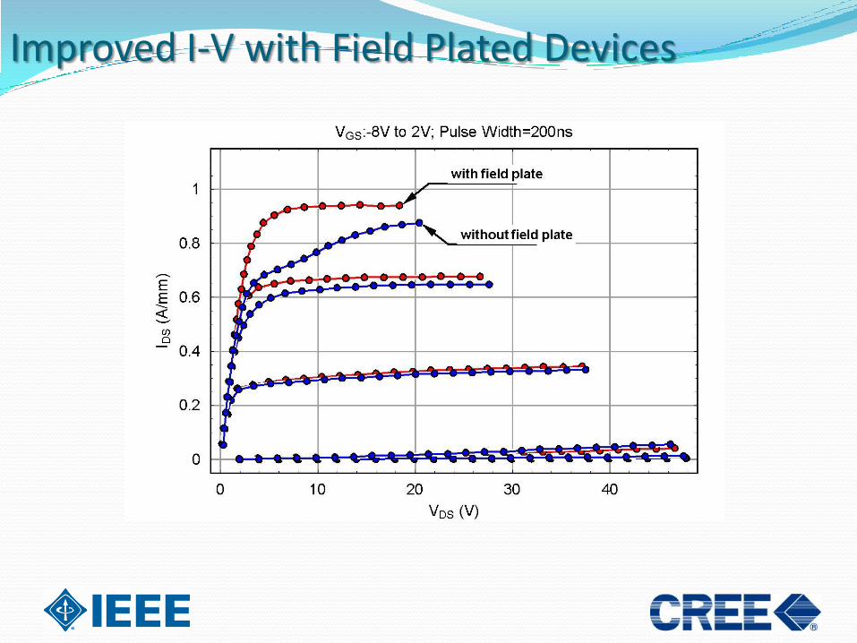
Improved I-V with Field Plated Devices

Typical Power Performance of Field Plated HEMTs

Blessings and Curses of High Power Density
At 28 volts, Cree GaN HEMTs have an RF power density of 4 watts per millimeter of gate periphery
At 48 volts, the same transistors have an RF power density of 8 watts per millimeter
At 65 volts, the same transistors have an RF power density of 11 watts per millimeter
With high operating voltages and power densities the design engineer has to be very aware of thermal management e.g. A CGH21120F transistor operating at 48 volts will generate 220 watts of
CW RF power and at PSAT have a drain efficiency of 65%
Dissipated heat is 118 watts – TRISE is 177OC – Needs de-rating The same device can operate at 35 volts producing 150 watts of CW power
with 70% drain efficiency
Dissipated heat is 64 watts – TRISE is 90OC – TCASE can be >100OC
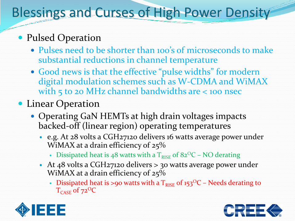
Blessings and Curses of High Power Density
Pulsed Operation Pulses need to be shorter than 100’s of microseconds to make
substantial reductions in channel temperature
Good news is that the effective “pulse widths” for modern digital modulation schemes such as W-CDMA and WiMAX with 5 to 20 MHz channel bandwidths are < 100 nsec
Linear Operation Operating GaN HEMTs at high drain voltages impacts
backed-off (linear region) operating temperatures e.g. At 28 volts a CGH27120 delivers 16 watts average power under
WiMAX at a drain efficiency of 25% Dissipated heat is 48 watts with a TRISE of 82OC – NO derating
At 48 volts a CGH27120 delivers > 30 watts average power under WiMAX at a drain efficiency of 25% Dissipated heat is >90 watts with a TRISE of 153OC – Needs derating to
TCASE of 72OC

General Purpose Application Insertions for GaN HEMTs
Emphasis usually on P1dB or saturated power, wide bandwidth and best efficiency
Applications include
Wideband, noisy, jammers
Software defined radios
Tactical communications
Phased array systems
Test instrumentation
Medical applications – e.g. ablation
Exciter applications – e.g. lighting
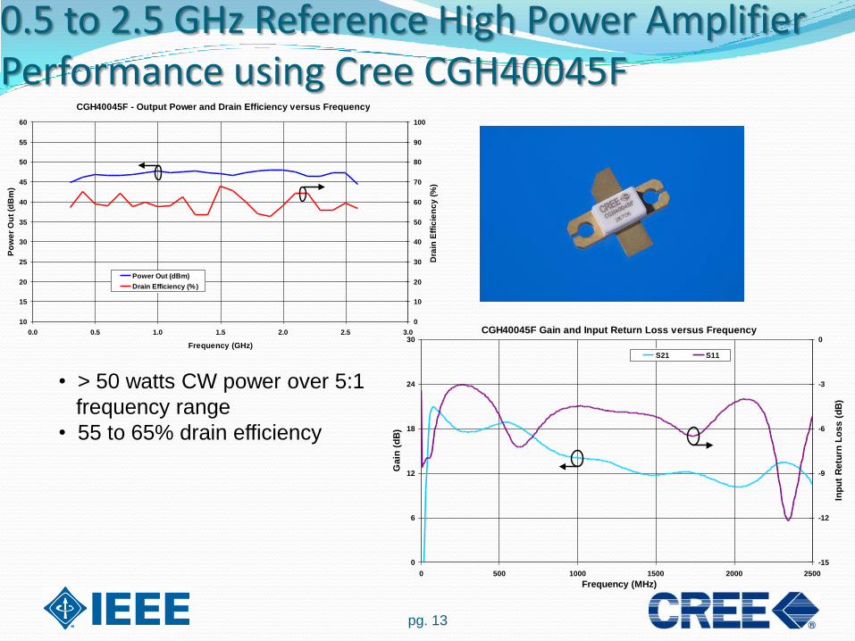
0.5 to 2.5 GHz Reference High Power Amplifier Performance using Cree CGH40045F
pg. 13
CGH40045F Gain and Input Return Loss versus Frequency
0
6
12
18
24
30
0 500 1000 1500 2000 2500
Frequency (MHz)
Gain
(d
B)
-15
-12
-9
-6
-3
0
Inp
ut
Retu
rn L
oss (
dB
)
S21 S11
CGH40045F - Output Power and Drain Efficiency versus Frequency
10
15
20
25
30
35
40
45
50
55
60
0.0 0.5 1.0 1.5 2.0 2.5 3.0
Frequency (GHz)
Po
we
r O
ut
(dB
m)
0
10
20
30
40
50
60
70
80
90
100
Dra
in E
ffic
ien
cy
(%
)
Power Out (dBm)
Drain Efficiency (%)
• > 50 watts CW power over 5:1
frequency range
• 55 to 65% drain efficiency

Performance of Push-Pull Power Amplifier for 0.5 to 2.5 GHz using Cree CGH40090PP
CGH40090PP -Output Power and Drain Efficiency versus Frequency
10
15
20
25
30
35
40
45
50
55
60
0.0 0.5 1.0 1.5 2.0 2.5 3.0
Frequency (GHz)
Po
we
r O
ut
(dB
m)
0
10
20
30
40
50
60
70
80
90
100
Dra
in E
ffic
ien
cy (
%)
Power Out (dBm)
Drain Efficiency (%)
CGH40090PP Gain and Drain Efficiency vs Output Power
0
10
20
30
40
50
60
20 25 30 35 40 45 50
Power Out (dBm)
Gain
(d
B)
0
10
20
30
40
50
60
Dra
in E
ffic
ien
cy (
%)
0.5 GHz Gain 1.0 GHz Gain 1.5 GHz Gain 2.0 GHz Gain 2.5 GHz Gain
0.5 GHz DE 1.0 GHz DE 1.5 GHz DE 2.0 GHz DE 2.5 GHz DE
Drain Efficiency is 50%

CGH40045F under Pulsed Stimulus at 50V drain voltage
pg. 15
CGH40045 Pulse Transfer
Vds=50V, 40uS Pulse 10% Duty Cycle, F=2.5GHz
0.0
10.0
20.0
30.0
40.0
50.0
60.0
70.0
0.0 5.0 10.0 15.0 20.0 25.0 30.0 35.0 40.0
Input Power (dBm)
Ou
tpu
t P
ow
er
(dB
m)
Dra
in E
ffic
ien
cy
(%
)
10.0
11.0
12.0
13.0
14.0
15.0
16.0
17.0
Gain
(d
B)
Pout
Drain Efficiency
Gain
100 watt
The CGH40045F GaN HEMT was originally designed for 28 volt
operation - Works well at 50 volts within thermal constraints
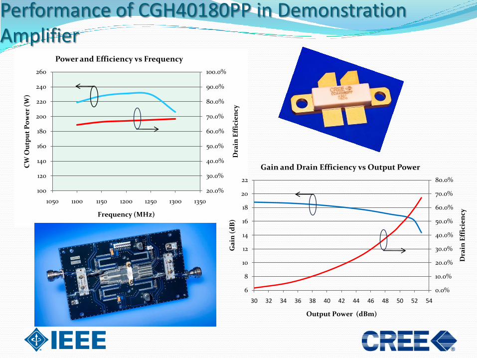
Performance of CGH40180PP in Demonstration Amplifier
20.0%
30.0%
40.0%
50.0%
60.0%
70.0%
80.0%
90.0%
100.0%
100
120
140
160
180
200
220
240
260
1050 1100 1150 1200 1250 1300 1350
Dra
in E
ffic
ien
cy
CW
Ou
tpu
t P
ow
er
(W)
Frequency (MHz)
Power and Efficiency vs Frequency
0.0%
10.0%
20.0%
30.0%
40.0%
50.0%
60.0%
70.0%
80.0%
6
8
10
12
14
16
18
20
22
30 32 34 36 38 40 42 44 46 48 50 52 54
Dra
in E
ffic
ien
cy
Ga
in (
dB
)
Output Power (dBm)
Gain and Drain Efficiency vs Output Power
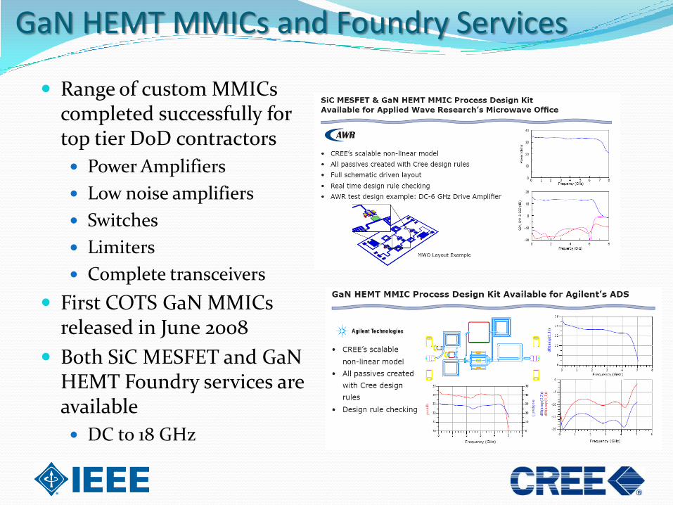
GaN HEMT MMICs and Foundry Services
Range of custom MMICs completed successfully for top tier DoD contractors
Power Amplifiers
Low noise amplifiers
Switches
Limiters
Complete transceivers
First COTS GaN MMICs released in June 2008
Both SiC MESFET and GaN HEMT Foundry services are available
DC to 18 GHz
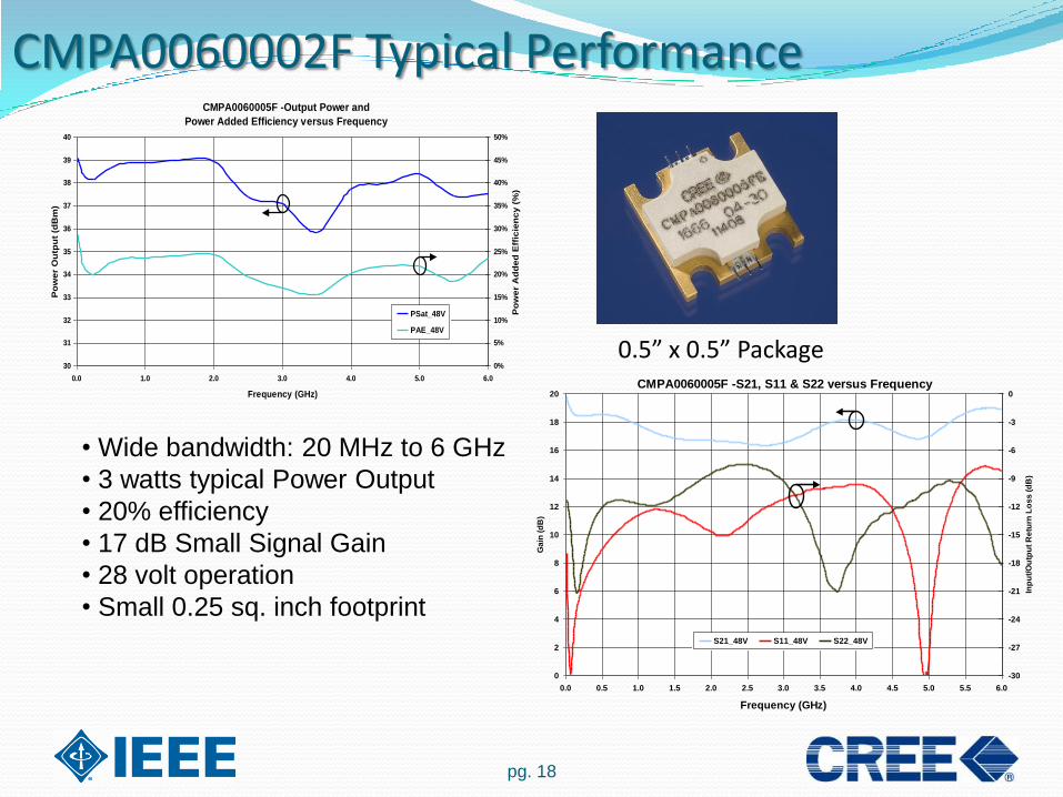
CMPA0060002F Typical Performance
pg. 18
CMPA0060005F -S21, S11 & S22 versus Frequency
0
2
4
6
8
10
12
14
16
18
20
0.0 0.5 1.0 1.5 2.0 2.5 3.0 3.5 4.0 4.5 5.0 5.5 6.0
Frequency (GHz)
Ga
in (
dB
)
-30
-27
-24
-21
-18
-15
-12
-9
-6
-3
0
Inp
ut/
Ou
tpu
t R
etu
rn L
os
s (
dB
)
S21_48V S11_48V S22_48V
CMPA0060005F -Output Power and
Power Added Efficiency versus Frequency
30
31
32
33
34
35
36
37
38
39
40
0.0 1.0 2.0 3.0 4.0 5.0 6.0
Frequency (GHz)
Po
we
r O
utp
ut
(dB
m)
0%
5%
10%
15%
20%
25%
30%
35%
40%
45%
50%
Po
we
r A
dd
ed
Eff
icie
nc
y (
%)
PSat_48V
PAE_48V
0.5” x 0.5” Package
• Wide bandwidth: 20 MHz to 6 GHz
• 3 watts typical Power Output
• 20% efficiency
• 17 dB Small Signal Gain
• 28 volt operation
• Small 0.25 sq. inch footprint

CMPA2560025F Typical Performance
pg. 19
Saturated Power Output and Power Added Efficiency versus Frequency
40
41
42
43
44
45
46
47
48
49
50
2.0 2.5 3.0 3.5 4.0 4.5 5.0 5.5 6.0 6.5
Frequency (GHz)
Sa
tura
ted
Po
we
r O
utp
ut
(dB
m)
0%
5%
10%
15%
20%
25%
30%
35%
40%
45%
50%
Po
we
r A
dd
ed
Eff
icie
nc
y (
%)
Typical Psat (dBm)
PAE at 44 dBm (%)
CMPA2560025F -S21, S11 & S22 versus Frequency
0
3
6
9
12
15
18
21
24
27
30
2.5 3.0 3.5 4.0 4.5 5.0 5.5 6.0
Frequency (GHz)
Gain
(d
B)
-20
-18
-16
-14
-12
-10
-8
-6
-4
-2
0
Inp
ut/
Ou
tpu
t R
etu
rn
Lo
ss (
dB
)
(S21) (S11) (S22)
0.5” x 0.5” Package
• Wide bandwidth: 2.5 to 6 GHz
• 25 watts typical Power Output
• 30% efficiency
• 24 dB Small Signal Gain
• 28 volt operation
• Small 0.25 sq. inch footprint
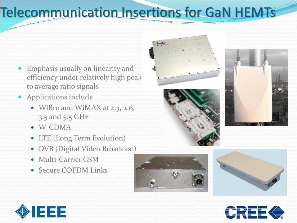
Telecommunication Insertions for GaN HEMTs
Emphasis usually on linearity and efficiency under relatively high peak to average ratio signals
Applications include
WiBro and WiMAX at 2.3, 2.6, 3.5 and 5.5 GHz
W-CDMA
LTE (Long Term Evolution)
DVB (Digital Video Broadcast)
Multi-Carrier GSM
Secure COFDM Links
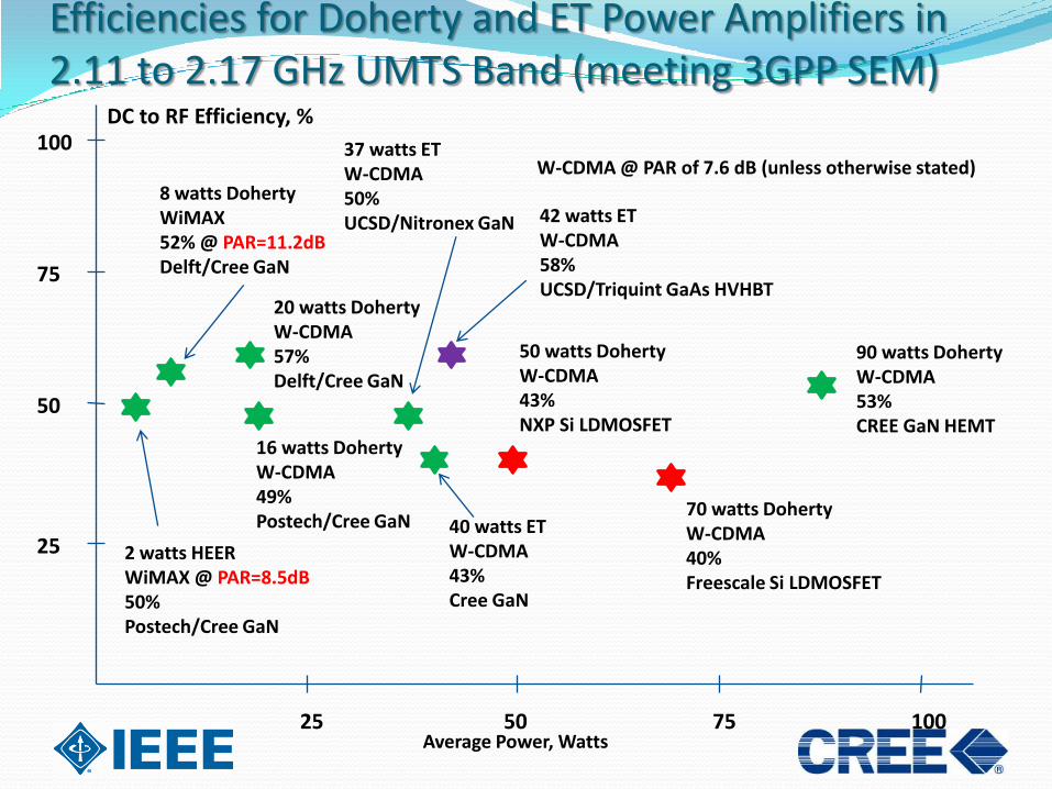
Efficiencies for Doherty and ET Power Amplifiers in 2.11 to 2.17 GHz UMTS Band (meeting 3GPP SEM)
DC to RF Efficiency, %
W-CDMA @ PAR of 7.6 dB (unless otherwise stated)
90 watts DohertyW-CDMA 53% CREE GaN HEMT
100
75
50
25
25 50 75 100
50 watts DohertyW-CDMA43% NXP Si LDMOSFET
20 watts DohertyW-CDMA57% Delft/Cree GaN
37 watts ETW-CDMA50% UCSD/Nitronex GaN
40 watts ETW-CDMA43% Cree GaN
70 watts DohertyW-CDMA40% Freescale Si LDMOSFET
8 watts DohertyWiMAX52% @ PAR=11.2dBDelft/Cree GaN
Average Power, Watts
2 watts HEERWiMAX @ PAR=8.5dB50% Postech/Cree GaN
16 watts DohertyW-CDMA49% Postech/Cree GaN
42 watts ETW-CDMA58% UCSD/Triquint GaAs HVHBT
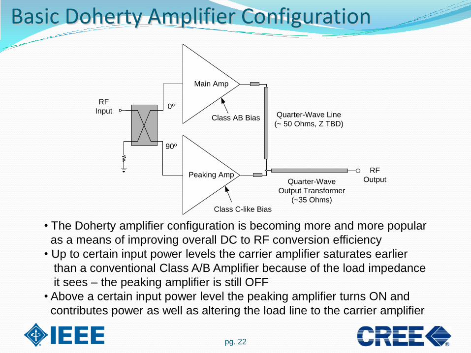
Basic Doherty Amplifier Configuration
pg. 22
RF
InputClass AB Bias
Class C-like Bias
Peaking Amp
Main Amp
Quarter-Wave Line
(~ 50 Ohms, Z TBD)
Quarter-Wave
Output Transformer
(~35 Ohms)
RF
Output
0o
90o
• The Doherty amplifier configuration is becoming more and more popular
as a means of improving overall DC to RF conversion efficiency
• Up to certain input power levels the carrier amplifier saturates earlier
than a conventional Class A/B Amplifier because of the load impedance
it sees – the peaking amplifier is still OFF
• Above a certain input power level the peaking amplifier turns ON and
contributes power as well as altering the load line to the carrier amplifier
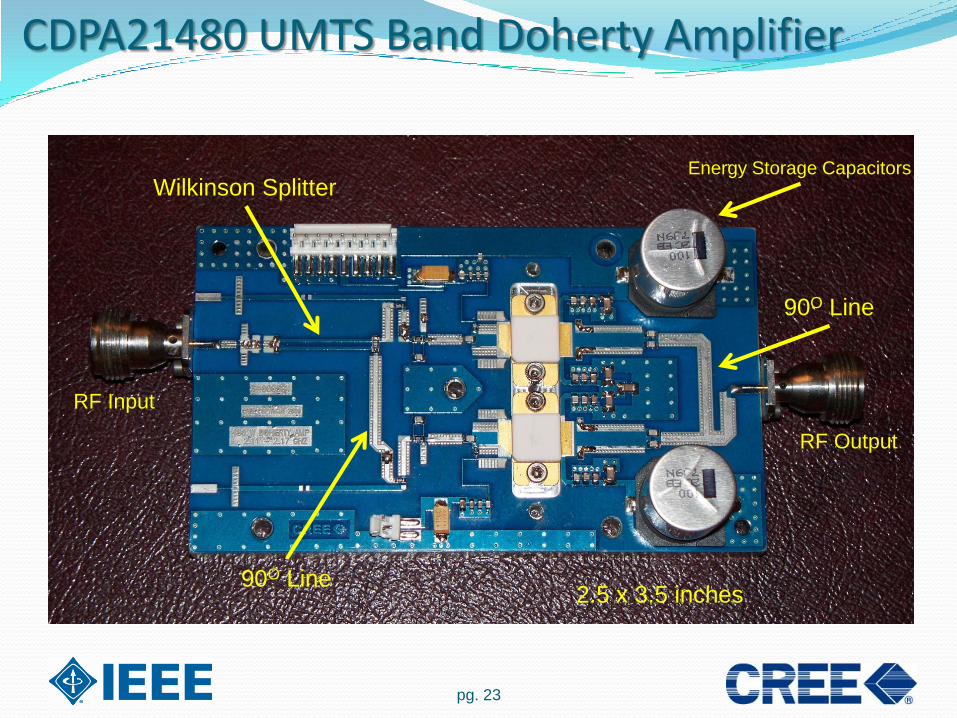
CDPA21480 UMTS Band Doherty Amplifier
pg. 23
Energy Storage Capacitors
90O Line
90O Line
Wilkinson Splitter
RF Input
RF Output
2.5 x 3.5 inches

Measured Single-Channel W-CDMA ACLR & Efficiency vs. RF Average Output Power
CGH21240DD WCDMA Transfer with & without DPDSingle Channel WCDMA, 6.8 dB PAR with CFR
Vds=50V, Idsq=600 mA, Frequency=2.14 GHz
-70
-65
-60
-55
-50
-45
-40
-35
-30
-25
-20
-15
28 30 32 34 36 38 40 42 44 46 48 50
WCDMA Average Output Power (dBm)
AC
LR
(d
Bc)
0%
5%
10%
15%
20%
25%
30%
35%
40%
45%
50%
55%
Dra
in E
ffic
ien
cy
ACLR-5 ACLR+5
ALT-10 ALT+10
ACLR-5 (PD) ACLR+5 (PD)
ALT-10 (PD) ALT+10 (PD)
Drain Effic (PD)

How Envelope Tracking (ET) Works
pg. 25
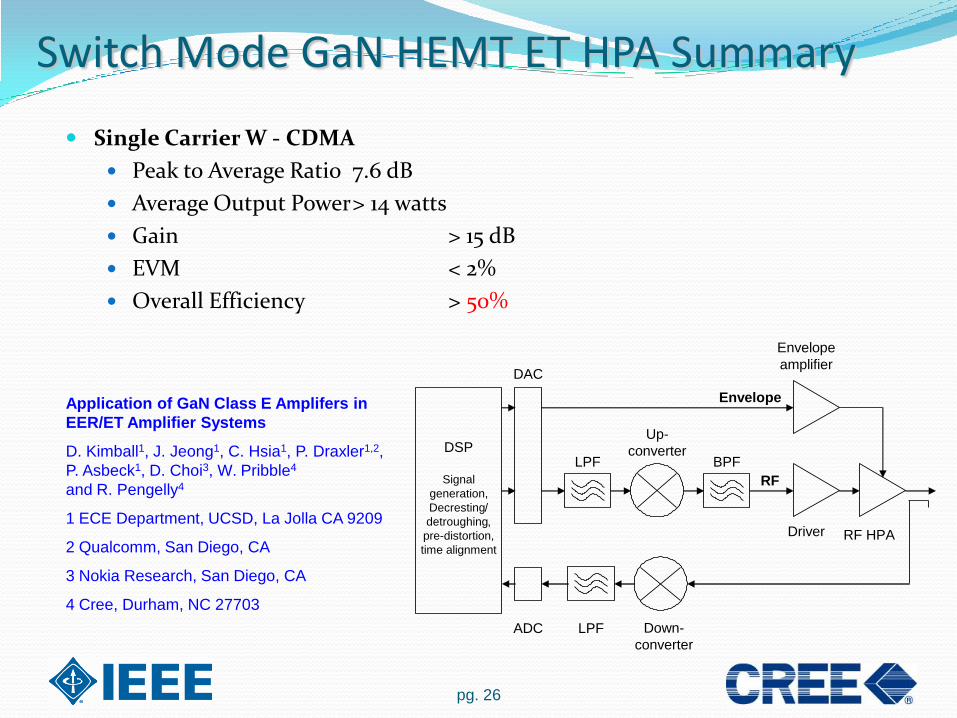
Switch Mode GaN HEMT ET HPA Summary
Single Carrier W - CDMA
Peak to Average Ratio 7.6 dB
Average Output Power> 14 watts
Gain > 15 dB
EVM < 2%
Overall Efficiency > 50%
pg. 26
DSP
Signal
generation,
Decresting/
detroughing,
pre-distortion,
time alignment
LPF
Up-
converterBPF
Driver RF HPA
Envelope
amplifier
Envelope
Down-
converterLPF
RF
ADC
DAC
Application of GaN Class E Amplifers in
EER/ET Amplifier Systems
D. Kimball1, J. Jeong1, C. Hsia1, P. Draxler1,2,
P. Asbeck1, D. Choi3, W. Pribble4
and R. Pengelly4
1 ECE Department, UCSD, La Jolla CA 9209
2 Qualcomm, San Diego, CA
3 Nokia Research, San Diego, CA
4 Cree, Durham, NC 27703

pg. 27
CGH21120F under compressed Class A/B
under Envelope Tracking (multi-carrier WCDMA)
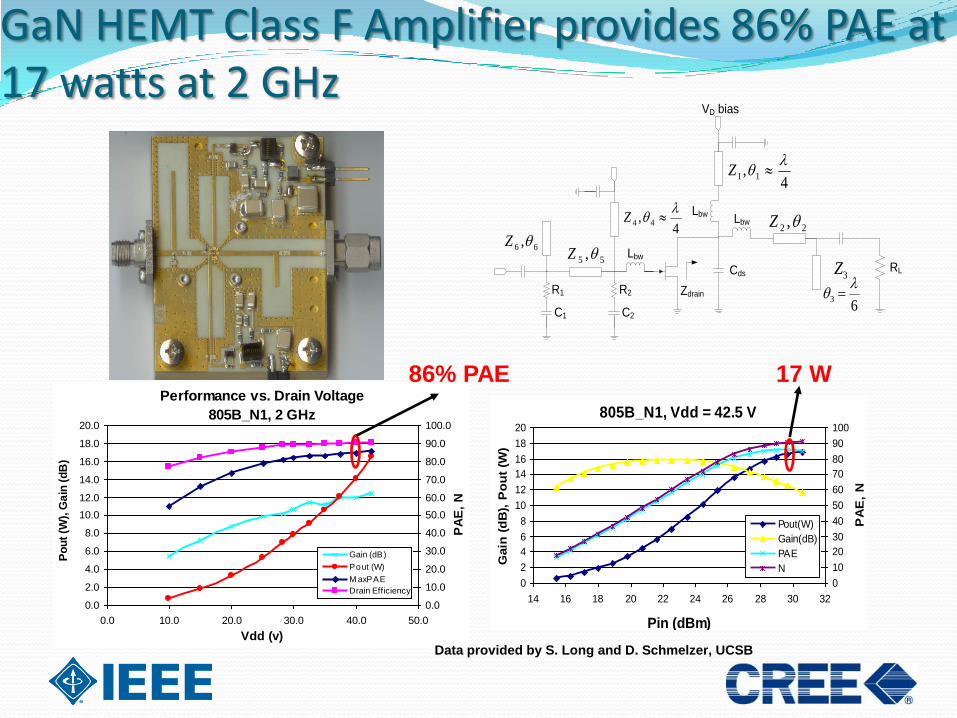
GaN HEMT Class F Amplifier provides 86% PAE at 17 watts at 2 GHz
805B_N1, Vdd = 42.5 V
0
2
4
6
8
10
12
14
16
18
20
14 16 18 20 22 24 26 28 30 32
Pin (dBm)
Gain
(d
B),
Po
ut
(W)
0
10
20
30
40
50
60
70
80
90
100
PA
E,
N
Pout(W)
Gain(dB)
PAE
N
Performance vs. Drain Voltage
805B_N1, 2 GHz
0.0
2.0
4.0
6.0
8.0
10.0
12.0
14.0
16.0
18.0
20.0
0.0 10.0 20.0 30.0 40.0 50.0
Vdd (v)
Po
ut
(W),
Ga
in (
dB
)
0.0
10.0
20.0
30.0
40.0
50.0
60.0
70.0
80.0
90.0
100.0
PA
E,
N
Gain (dB)
Pout (W)
M axPAE
Drain Efficiency
Lbw Lbw
Cds RL
22 ,Z
4, 11
Z
3Z
63
Zdrain
VD bias
Lbw55 ,Z66 ,Z
C1
R1
C2
R2
4, 44
Z
86% PAE 17 W
Data provided by S. Long and D. Schmelzer, UCSB

Effect of Efficiency on Transistor Operating Temperature
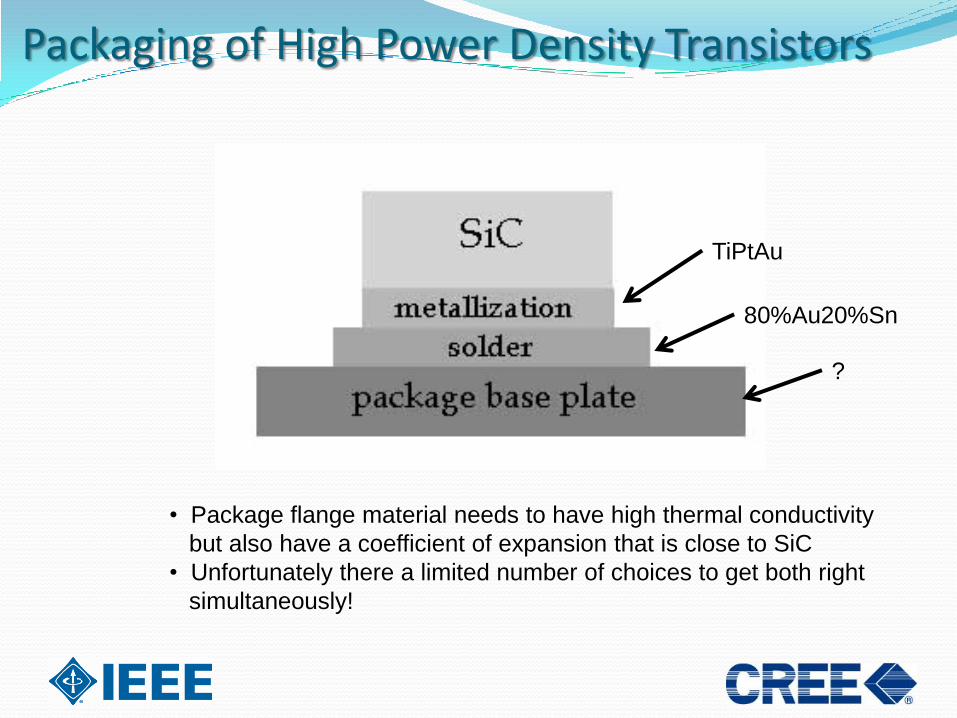
Packaging of High Power Density Transistors
TiPtAu
80%Au20%Sn
?
• Package flange material needs to have high thermal conductivity
but also have a coefficient of expansion that is close to SiC
• Unfortunately there a limited number of choices to get both right
simultaneously!

Properties of Relevant MaterialsMaterial Structure Thermal
ConductivityW/mK
Coefficient of Thermal
Expansionppm/K
Cu Pure 393 17
Diamond 1500 1.4
Silicon 136 4.1
SiC 4H-SI 430 4
AlSiC 63%SiC >175 7.9
W90Cu 90% W 185 6.5
W75Cu 75% W 225 9
Mo70Cu 70% Mo 185 9.1
Mo50Cu 50% Mo 250 11.5
CuMoCu 1:4:1 220 6
CuMoCu 1:1:1 310 8.8
Cu/Mo70Cu/Cu 1:4:1 laminate 340 8

Thermal ImprovementsAt the transistor level
New power transistor layouts to reduce junction temperature at constant power density
At the package level
• New flange materials with
higher thermal conductivityand CTE match to SiC
• Present CuW is ~200 W/mK• New SuperCMC is 350 W/mK
• Aluminum diamond
is 550 W/mK
Presentlayout
NewLayoutprovides20% reduction in operatingtemperatures
TJ decreases by 10%
TJ decreases by further 15%
Combined lowers 175 C junction temperature to123 C
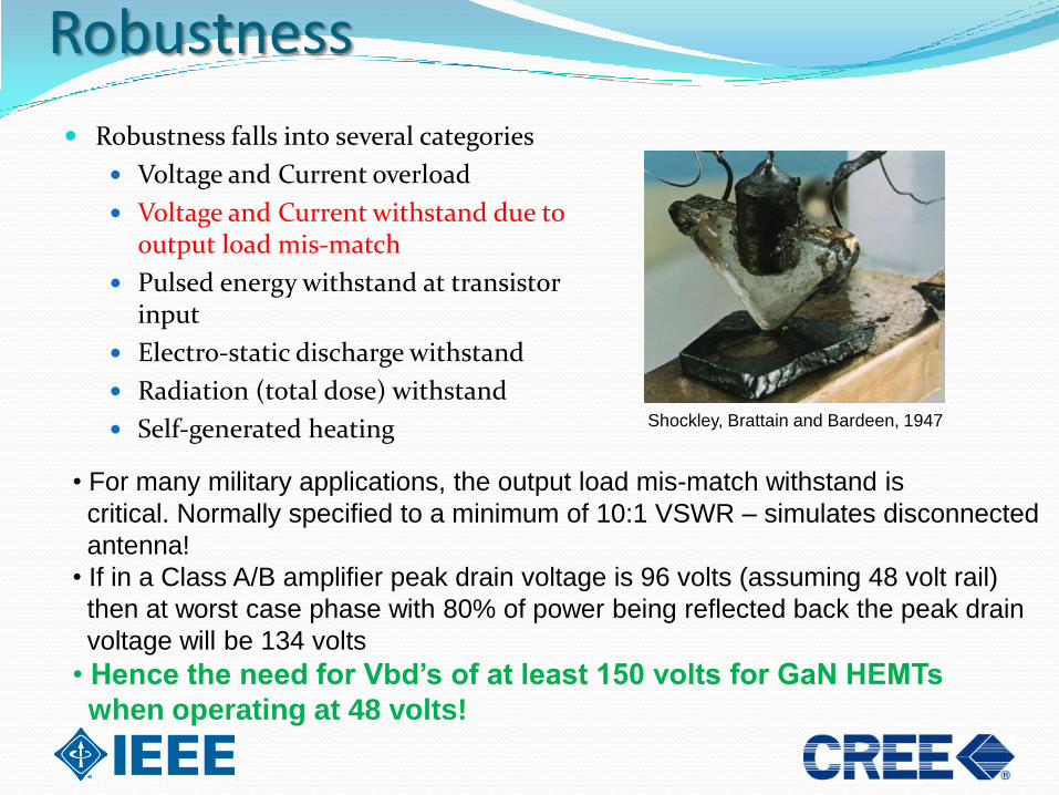
Robustness
Robustness falls into several categories
Voltage and Current overload
Voltage and Current withstand due to output load mis-match
Pulsed energy withstand at transistor input
Electro-static discharge withstand
Radiation (total dose) withstand
Self-generated heating
• For many military applications, the output load mis-match withstand is
critical. Normally specified to a minimum of 10:1 VSWR – simulates disconnected
antenna!
• If in a Class A/B amplifier peak drain voltage is 96 volts (assuming 48 volt rail)
then at worst case phase with 80% of power being reflected back the peak drain
voltage will be 134 volts
• Hence the need for Vbd’s of at least 150 volts for GaN HEMTs
when operating at 48 volts!
Shockley, Brattain and Bardeen, 1947

Reliability - Cree GaN vs. other GaN Suppliers
101
102
103
104
105
106
10
150
175
200
225
250
275
300
325
350
375
400425
Te
mp
era
ture
(deg
. C
)
MTTF (hours)
710
810
9
Cree GaN on SiC
Cree GaN
GaN on Si under DC
operation
E a = 2.0 eV
GaN on SiC
Ea = 1.3 eV
Supplier T GaN
GaN on Si
Ea
= 1.6 eV
Cree GaN devices are the most reliable in the industry
580 million Cree device hours in the field

Higher Frequencies
Switches, LNA’s etc.

MMIC Switches Separate RF and Control
Ports
No need for Chokes
Takes no control current
PIN diode replacement
High Power Operation
Wideband Operation
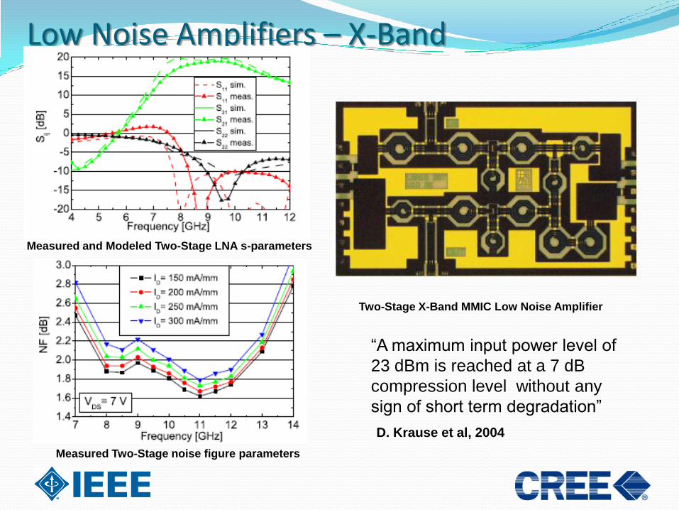
Low Noise Amplifiers – X-Band
Two-Stage X-Band MMIC Low Noise Amplifier
Measured and Modeled Two-Stage LNA s-parameters
Measured Two-Stage noise figure parameters
D. Krause et al, 2004
“A maximum input power level of
23 dBm is reached at a 7 dB
compression level without any
sign of short term degradation”
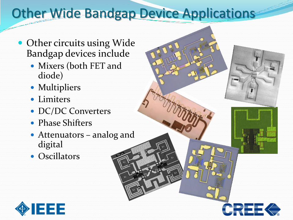
Other Wide Bandgap Device Applications
Other circuits using Wide Bandgap devices include Mixers (both FET and
diode)
Multipliers
Limiters
DC/DC Converters
Phase Shifters
Attenuators – analog and digital
Oscillators

90 nm GaN HEMT Technology for mm-waves

Performance of GaN HEMTs at mm-waves
(passivated – higher capacitance)

Acknowledgements I would like to acknowledge the assistance
of my Cree colleagues in preparing this presentation
Ulf Andre
Don Farrell
Don Gajewski
Chris Harris
Jim Milligan
Brad Millon
Carl Platis
Art Prejs
Bill Pribble
Scott Shephard
Simon Wood