random telegraph noise in 3d nand flash memories
TRANSCRIPT

micromachines
Review
Random Telegraph Noise in 3D NAND Flash Memories
Alessandro S. Spinelli * , Gerardo Malavena , Andrea L. Lacaita and Christian Monzio Compagnoni
�����������������
Citation: Spinelli, A.S.; Malavena, G.;
Lacaita, A.L.; Monzio Compagnoni, C.
Random Telegraph Noise in 3D
NAND Flash Memories.
Micromachines 2021, 12, 703.
https://doi.org/10.3390/mi12060703
Academic Editors: Cristian Zambelli
and Rino Micheloni
Received: 11 May 2021
Accepted: 4 June 2021
Published: 16 June 2021
Publisher’s Note: MDPI stays neutral
with regard to jurisdictional claims in
published maps and institutional affil-
iations.
Copyright: © 2021 by the authors.
Licensee MDPI, Basel, Switzerland.
This article is an open access article
distributed under the terms and
conditions of the Creative Commons
Attribution (CC BY) license (https://
creativecommons.org/licenses/by/
4.0/).
Dipartimento di Elettronica, Informazione e Bioingegneria, Politecnico di Milano, 20133 Milan, Italy;[email protected] (G.M.); [email protected] (A.L.L.); [email protected] (C.M.C.)* Correspondence: [email protected]; Tel.: +39-02-2399-4001
Abstract: In this paper, we review the phenomenology of random telegraph noise (RTN) in 3DNAND Flash arrays. The main features of such arrays resulting from their mainstream integra-tion scheme are first discussed, pointing out the relevant role played by the polycrystalline natureof the string silicon channels on current transport. Starting from that, experimental data for RTNin 3D arrays are presented and explained via theoretical and simulation models. The attention isdrawn, in particular, to the changes in the RTN dependences on the array working conditions thatresulted from the transition from planar to 3D architectures. Such changes are explained by consider-ing the impact of highly-defective grain boundaries on percolative current transport in cell channelsin combination with the localized nature of the RTN traps.
Keywords: 3D NAND Flash memories; random telegraph noise; Flash memory reliability
1. Introduction
Random telegraph noise (RTN) in MOS transistors has been an important topic of in-terest in the solid-state device community since the 80s, when results of low-frequencynoise characterization [1] showed a transition from a typical 1/ f behavior at high tem-peratures to a series of discrete switching events as temperature was lowered. Similarobservations were soon made when moving from large- to small-area devices [2], andinterpreted in terms of capture/emission of electrons by single interface traps. On thetheoretical side, this result highlighted the importance of the number fluctuation contribu-tion to the flicker noise, but prompted the emergence of a new limitation to MOS deviceoperation as well [3].
Moving from early investigations and models [4–9], the RTN picture grew more complex,as novel time and amplitude observations [10–14] hinted at a non-negligible role played bynon-uniform electron conduction in submicron devices [15,16]. This idea gained traction whenthe phenomenon began to be investigated in Flash memories [17–23], demonstrating currentfluctuations up to 60% [22] and threshold voltage (VT) shifts reaching 700 mV [18] in 90-nmtechnology node devices. The physical picture now accepted that accounts for such resultsis based on the fact that, in scaled devices, dopants must be viewed as individual ionsrather than a continuous distribution, resulting in randomly-placed charges in the deple-tion region. Such random point charges [24–27] give rise to sharp peaks in the band energyprofile of the channel of an MOS transistor, resulting in local modulation of the current flowand filamentary conduction. If a “strategic” trap happens to be placed right above a currentpath, electron trapping will effectively shut off such a path, resulting in a large drain currentand VT fluctuation [28–31]. On the other hand, if the trap is placed over a region in whichlittle current flows, its trapping/detrapping will barely affect the overall current. Suchan idea has been successfully applied to explain the statistical distribution of the RTN fluc-tuations in NOR and NAND arrays, measured in terms of their amplitude [19,32,33] andtime constants [34–36], providing a useful tool for extracting information about the impactof device parameters on RTN. A recent review of the issue can be found in [37].
The above-mentioned framework has served nicely the Flash community until the firstdecade of the 21st century, when several limitations to the scaling of the planar NAND
Micromachines 2021, 12, 703. https://doi.org/10.3390/mi12060703 https://www.mdpi.com/journal/micromachines

Micromachines 2021, 12, 703 2 of 14
technology prompted the emergence of 3D arrays [38]. In such devices, the RTN picture justoutlined fell short of adequately describing the experimental data, in view of the peculiarcharacteristics of the polycrystalline material used as conduction channel.
In the following, we will review in detail the physics of RTN in 3D NAND Flashmemories, discussing the main experimental data and physical models developed to quan-titatively account for them. We begin our discussion with a brief summary of the main 3Darray architecture and cell structure, followed by a description of electron transport in3D NAND channels. This will allow us to develop a consistent picture of RTN in 3DNAND devices, whose main features will be highlighted. After this part, we will focusour attention on the main experimental data presented in the literature, taking advantageof the model results to provide interpretation for them.
2. Array and Cell Structure
Among the several architectural solutions for 3D storage [39–46], the one employingvertical-channel strings crossed by a set of planar wordlines has become the most effectiveone [47–50], and is the focus of this section. Here we will briefly describe the main featuresof such an array, namely its organization and cell structure, referring to previous worksfor further details [51].
A pictorial view of the array is shown in Figure 1 (left): note that the cell strings runvertically from the substrate to the bitlines. As in planar arrays, select elements are needednear the source and drain ends of the string, integrated in rows running orthogonallyto the bitlines. The rest of the cells are contacted by planar wordlines that span overan entire block of the array. One of the advantages of this structure is that the large increasein density allowed by the exploitation of the third dimension makes it possible to relievesome of the pressure on channel length scaling and its many drawbacks from the viewpointof process complexity and reliability, well known in planar devices [52,53]: cell length in 3DNAND is around 25–30 nm [54], with the additional advantage of becoming less dependenton the availability of advanced lithography tools. A second advantage of this solution liesin its manufacturing process: memory cells are not patterned individually, but they areformed all at once as cylindrical holes are cut through the stacked wordlines, creatingthe strings. This procedure entails that the elementary cell becomes a gate-all-around,vertical-channel transistor, with the advantage of a better electrostatic control from the gate.A schematic view of such a device is shown in Figure 1 (right): starting from the outside wemeet a contacted wordline, a blocking dielectric and a charge-storage layer, that can eitherbe a floating gate [47,55–59], similar to planar NAND devices, or a charge-trap layer [60–64],followed by the tunnel oxide. Beyond the oxide, we can notice a thin silicon region andan inner oxide filling the central region of the cylinder, labeled filler oxide for simplicity.This structure, where the conductive channel is a hollow cylinder, is referred to as a“Macaroni” MOSFET, and is the result of clever device engineering in 3D NAND: in fact,after the vertical high-aspect ratio holes have been etched in the structure of Figure 1 (left),and the blocking, storage and tunnel layers deposited, the remaining part of the cylindermust be filled with silicon. The result is a polycrystalline channel whose central region isplagued by a large defectivity, impairing the device performance. To avoid such a drawback,a very thin polysilicon layer is deposited on the gate dielectric, while the remaining centralregion of the cylinder is filled with a dielectric [40], gaining two distinct advantages: first,thinning of the silicon body results in reduced short-channel effects and better electrostaticcontrol from the gate; second, defect removal further contributes to better subthresholdslope and array performance.

Micromachines 2021, 12, 703 3 of 14
Figure 1. (Left) Conceptual view of a vertical-channel 3D NAND array with its main elements(SSL = source select line, WLs = wordlines, DSL = drain select line, BLs = bitlines). (Right) pictorialview of an array string highlighting the structure of the elementary memory cells.
3. Polysilicon Conduction
The overview on the memory cell design given in the previous section already sug-gested that the polycrystalline character of the conduction channel is a key parameter fromthe viewpoint of device performance. A polycrystalline material, in fact, is formed bysingle-crystal regions labeled grains, with different crystallographic orientations. Suchregions are separated by highly-defective interfaces, or grain boundaries (GBs) [65]. A pic-torial view of a NAND string of ten cells with its inner polysilicon region and grains isshown in Figure 2: note the random structure of grains and GBs, that are the key elementsaffecting device current and variability.
Figure 2. Pictorial view of a ten-cell memory string (left) and of the inner polysilicon regionsseparated into polycrystalline grains (right). The example is the result of a TCAD simulation ofthe cell structure where polysilicon grains are obtained via Voronoi tessellation of the silicon region.
One of the key properties of polysilicon is its trap density, whose value has beenestimated by several works, based on either direct optical or electrical experimental mea-surements [66–74] or via numerical device simulations [75–79]. Many of such resultspoint to a double-exponential energy distribution of donor-like and acceptor-like statesof the form (for acceptor-like states in the upper half of the energy gap):
NGB(E) = NTe−(E−EC)/ET + NDe−(E−EC)/ED , (1)
where the reported range for the acceptor-like states parameters is listed in Table 1. Notethat the first exponential distribution is characterized by a large peak density NT and asmall characteristic energy ET , and is usually referred to as tail states distribution, as a con-sequence of its location near the edge of the gap. The second has a lower peak densityND but a higher energy ED, and is usually labeled deep states distribution. Note also that
Micromachines 2021, 12, 703 4 of 14
trap densities are given as volumetric densities: this was useful in early simulation works,where a uniform trap density in the semiconductor body was assumed for simplicity. Froma physical viewpoint, however, traps are expected to be mainly located at GBs, and an arealdensity σ is then needed. A conversion between volumetric and areal densities is readilyachieved assuming for simplicity a spherical grain size with radius rG, and placing allvolume traps on the sphere surface. This leads to
4πr2Gσ =
43
πr3G NGB ⇒ σ =
rG3
NGB, (2)
or a very similar conversion factor as in [79].
Table 1. Range of parameter values for the acceptor-like states in the polysilicon, according to the lit-erature (see text for references).
NT [cm−3 eV−1] ET [meV] ND [cm−3 eV−1] ED [meV]
9× 10¹⁹–1021 16.6–80 1.2× 10¹⁸–9 ×10¹⁹ 80–500
Electron transport in polysilicon has been studied since the 70s, as this material foundapplications in resistors, interconnections, and silicon-gate MOSFETs. From the viewpointof current conduction, we can identify two modeling approaches, that differ in the way GBsare treated: one approach is to extend the drift-diffusion model usually adopted in monocrys-talline silicon, describing GBs as trapping centers with a reduced mobility [80–82]; the other isbased on a thermionic emission model at the GBs [83–87]. Although the latter seems to begaining traction in recent literature, a definitive conclusion has not been reached, yet, and arecent study of the different dependences implied by such models can be found in [88,89].
The above-mentioned numerical models of conduction have been used to investigatethe effect of GBs on variability in nanowires [90–95] and 3D NAND devices [96,97]. A re-cent study based on a drift-diffusion transport within the grains and thermionic emission atthe GBs [98–101] has demonstrated a good capability to reproduce several features ofexperimental data, including its temperature dependence. Figure 3 (left) shows a typicalconduction-band profile along the channel of a 3D NAND string, for increasing valuesof the control-gate bias, as resulting from such model. Note that the profile is not smooth,featuring peaks in correspondence of the highly-defective GBs. As gate bias is increased,the band bending lowers the conduction-band profile, increasing the localized trap occu-pation and sharpening the peaks, which become the true bottlenecks of conduction [100].This result makes clear that GBs are an additional source of non-uniformity in the currentconduction, which means that they might be expected to play a main role in RTN. Thisis even more apparent if we consider that GB trap densities (see Table 1) are much largerthan typical doping concentrations used in 3D NAND strings. A similar approach was alsofollowed by [102].
The above-mentioned model has been applied to investigate the impact of GB trapson RTN [99,101] within a Monte Carlo approach: random configuration of GBs are firstgenerated in the silicon region after a Voronoi tessellation [92], and traps are placed atthe interfaces following the previously-discussed energy distribution. Drain current iscomputed up to a specified threshold, defined at a constant current level, after whichan additional RTN trap is filled with an electron and the resulting VT shift computed.Results for a template device are also reported in Figure 3, for the case of a single trapplaced at one random position in a GB, and for a trap placed at a random position at thesilicon/gate oxide interface. It is clear that GB traps are much more effective in modulatingthe electron conduction and result in larger VT fluctuations.

Micromachines 2021, 12, 703 5 of 14
500 600 700Distance[nm]
-0.4
-0.3
-0.2
-0.1
0
0.1
0.2
Ener
gy[e
V]
I=10-10AI=10-8AI=10-6A
Figure 3. (Left) Conduction band profile for a 3D NAND string at different current levels. (right)RTN complementary cumulative distribution functions (ccdfs) for traps placed at the GBs or atthe gate/oxide interface for a template device.
In spite of these encouraging results, several important features of this model stillhave to be assessed, such as the actual grain size [103–105], the mobility degradation andconduction process at the grain boundaries [106,107], and the impact of all these quantities,including architectural parameters and cell design, on RTN.
4. Experimental Data
The previous section was meant to provide a framework for the interpretation of the mostrelevant experimental data presented in the literature, that are discussed in the following. Itmust be noted, however, that RTN, as well as other reliability concerns in 3D NAND memories,remains a highly-confidential matter and very few data are published. We begin our analysisof RTN with single-trap data, moving then to statistical distributions and impact on deviceperformance.
4.1. Single-Trap Data
Investigation of the microscopic properties of RTN single traps in 3D NAND de-vices can be found in [108,109], where a statistical analysis of the noise power spectraldensity was also carried out. In those papers it was reported that the string current fluctua-tions due to single-trap RTN depend on the sensing current: as the current is increased,its fluctuations also increase when measured in absolute terms, but decrease in termsof relative change. Such a dependence was also found in [110] for the above-thresholdregion, and ascribed to the effect of traps at the silicon-oxide interfaces. These depen-dences reflect similar behaviors observed both experimentally and numerically in planaror cylindrical devices [111–113], where the increased screening exerted by the mobilecarriers as the gate bias is raised, mitigating the effect of the RTN trap, was invoked asan explanation. Several works reported investigations of the capture and emission timeconstants and their dependence on gate bias and temperature, including the activation en-ergies [114–117]. Their results do not point to any particular difference in the microscopicnature of such traps with respect to those active in planar devices (apart from a faster cap-ture/emission dynamics suggested in [114]): this of course is not surprising and supportsan interpretation of the RTN phenomenon based on the spatial distribution of such trapsrather than on some peculiar characteristics.
4.2. Array Statistical Data
From the viewpoint of the memory performance, the statistical distribution of the RTN-induced ∆VT is the main parameter. This kind of fluctuations in poly-Si channels werefirst shown (to our knowledge) in [118], on a nanowire structure (no filler oxide), showingan exponential distribution for ∆VT , which is a typical result of a percolation process.The same exponential dependence was reported on vertical NAND devices in [119–123],suggesting that the RTN distribution in arrays follows an e−∆VT/λ law, and can be effectivelycharacterized by the slope λ of the exponential distribution.
Micromachines 2021, 12, 703 6 of 14
A comparison between 3D and planar cell RTN is reported in [124], where a largerRTN distribution was reported for the former, while an opposite result was claimedin [121]. It is obviously difficult if not impossible to critically assess those results andsearch for the reason of this discrepancy. However, from a general standpoint, the slope λis related to both the trap density (affecting the percolation centers) and the electrostaticimpact of a single trapped electron, that have an opposite trend when moving from planarto 3D devices: 3D cells are expected to have a higher trap density thanks to the presenceof GBs, but feature also a larger cell (i.e., a larger capacitance and a lower electrostaticimpact of a single electron). So, the different results might just be a consequence of differentcell designs.
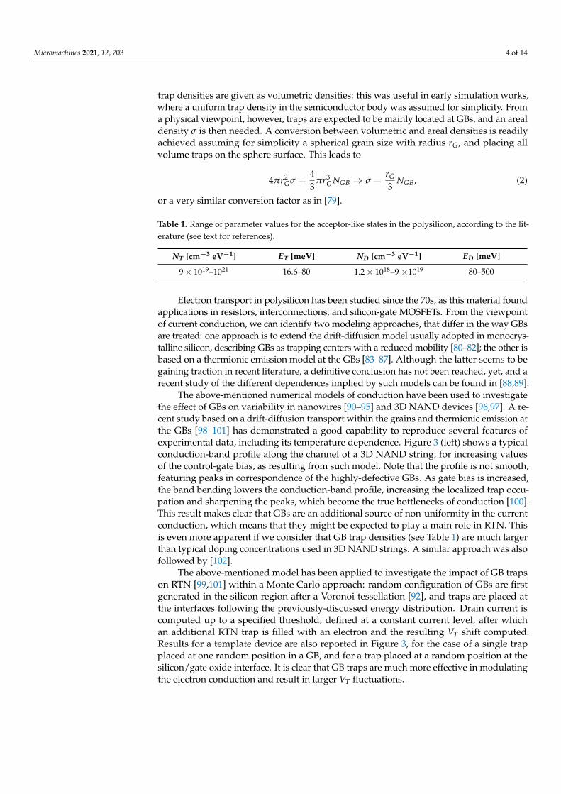
The impact of GB traps on RTN can also be noted in the comparison reported in [125,126]and carried out as a function of temperature in the range from −10 to 125 ◦C, that is shownin Figure 4 (left). First, please note that the shape of the two distributions is different: in 2Dcells we notice clear exponential tails due to RTN departing from a central distribution,related to measurement noise in cells not affected by RTN; in 3D arrays, instead, we notice asingle exponential distribution, suggesting that the large majority of cells in the 3D array areaffected by RTN. A second point to stress is that the slope of the exponential distribution isreduced with respect to planar technologies [121,125,127]. Given the previous point, suchan improvement seems mainly a consequence of the larger cell size of 3D arrays, although arole could also be played by the different conduction mechanism and percolation in planarand 3D devices (see for example [113] for a discussion on the RTN dependences in 3Ddevices). Finally, different temperature dependences are also apparent: while planardevice RTN is temperature-independent [128], 3D NAND exhibit a decrease in λ at highertemperatures, as also reported in [115,116].
-1 -0.5 0 0.5 1DVT[a.u.]
10-6
10-5
10-4
10-3
10-2
10-1
100
cdf,
ccdf
-1 -0.5 0 0.5 1DVT[a.u.]
10-6
10-5
10-4
10-3
10-2
10-1
100
cdf,
ccdf
T=-10°CT=55°CT=125°C
2DNAND 3DNAND
0 50 100 150 200Time[s]
0
0.25
0.5
0.75
1
V T[a.u
.]
T=160KT=180KT=200K
Figure 4. (Left) RTN cumulative density function (cdf) and its complementary (ccdf) for 2D and 3DNAND arrays at different temperatures [125,126], © 2017, IEEE. (Right) VT fluctuations due to singleRTN traps at different temperatures.
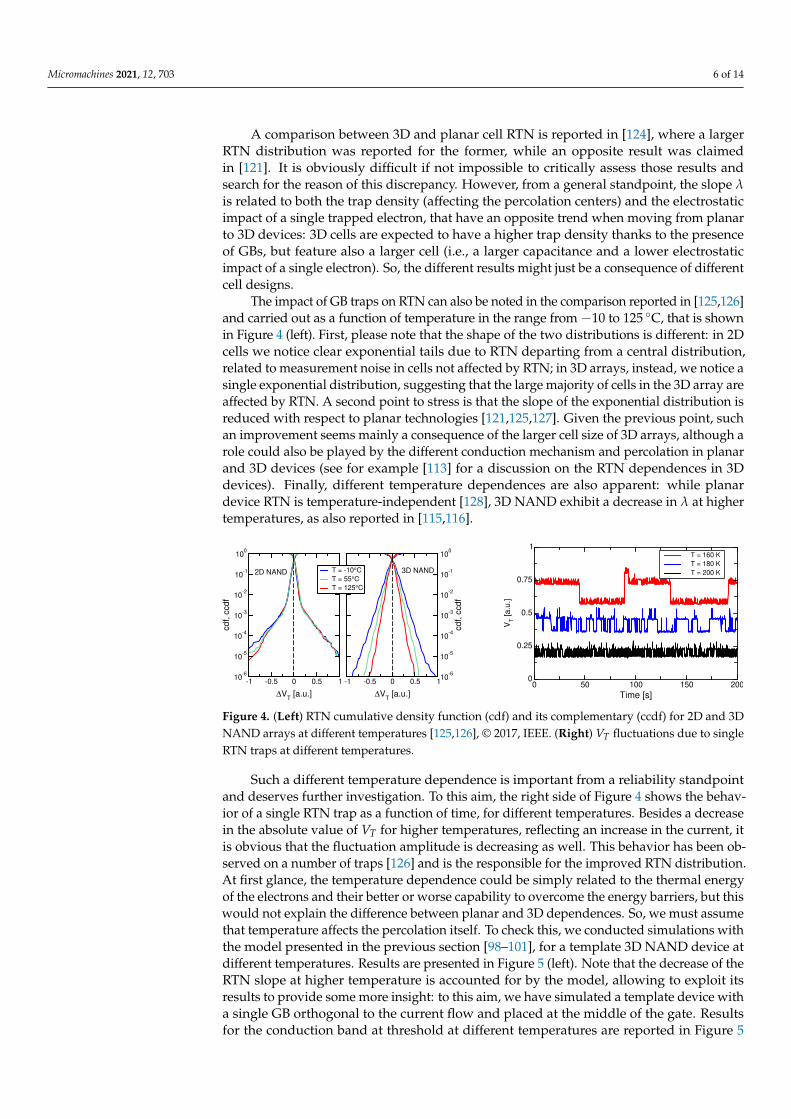
Such a different temperature dependence is important from a reliability standpointand deserves further investigation. To this aim, the right side of Figure 4 shows the behav-ior of a single RTN trap as a function of time, for different temperatures. Besides a decreasein the absolute value of VT for higher temperatures, reflecting an increase in the current, itis obvious that the fluctuation amplitude is decreasing as well. This behavior has been ob-served on a number of traps [126] and is the responsible for the improved RTN distribution.At first glance, the temperature dependence could be simply related to the thermal energyof the electrons and their better or worse capability to overcome the energy barriers, but thiswould not explain the difference between planar and 3D dependences. So, we must assumethat temperature affects the percolation itself. To check this, we conducted simulations withthe model presented in the previous section [98–101], for a template 3D NAND device atdifferent temperatures. Results are presented in Figure 5 (left). Note that the decrease of theRTN slope at higher temperature is accounted for by the model, allowing to exploit itsresults to provide some more insight: to this aim, we have simulated a template device witha single GB orthogonal to the current flow and placed at the middle of the gate. Resultsfor the conduction band at threshold at different temperatures are reported in Figure 5
Micromachines 2021, 12, 703 7 of 14
(right), and feature significant differences: indeed, the conduction band peak, located atthe GB and due to the localized trapped charge, becomes sharper at low temperatures,meaning that there is an increased trapped charge at low temperatures, resulting in morepercolation centers. A reason for this lies in our definition of the threshold condition, thatis a constant-current (10 nA) criterion. When temperature is lowered, thermal emission isreduced, and the string current lowers. To reach the same 10 nA value, gate bias must beincreased, lowering the conduction band and leading to additional trap filling. Note alsothat this phenomenon does not take place in planar devices, where the percolation centersare the ionized dopants, whose density obviously does not change with the gate bias.
0 20 40 60 80 100Distance[nm]
-0.6
-0.4
-0.2
0
0.2
0.4
Con
duct
ion
band
[eV]
T=400KT=350KT=300KT=250KT=200K
Figure 5. (Left) Simulation results for the RTN ccdf in a template 3D NAND device for differenttemperatures. (Right) Conduction band profile at different temperatures for a template device with asingle GB located at the center of the channel.
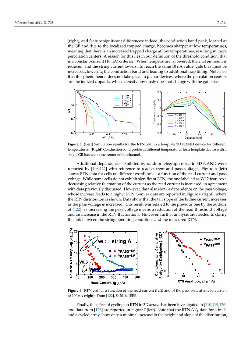
Additional dependences exhibited by random telegraph noise in 3D NAND werereported by [108,122] with reference to read current and pass voltage. Figure 6 (left)shows RTN data for cells on different wordlines as a function of the read current and passvoltage. While some cells do not exhibit significant RTN, the one labelled as WL2 features adecreasing relative fluctuation of the current as the read current is increased, in agreementwith data previously discussed. However, data also show a dependence on the pass voltage,whose increase leads to a higher RTN. Similar data are reported in Figure 6 (right), wherethe RTN distribution is shown. Data show that the tail slope of the bitline current increasesas the pass voltage is increased. This result was related to the previous one by the authorsof [122], as increasing the pass voltage means a reduction of the read threshold voltageand an increase in the RTN fluctuations. However, further analysis are needed to clarifythe link between the string operating conditions and the measured RTN.
Figure 6. RTN ccdf as a function of the read current (left) and of the pass bias, at a read currentof 100 nA (right). From [122], © 2016, IEEE.
Finally, the effect of cycling on RTN in 3D arrays has been investigated in [110,119,126]and data from [126] are reported in Figure 7 (left). Note that the RTN ∆VT data for a freshand a cycled array show only a minimal increase in the height and slope of the distribution,

Micromachines 2021, 12, 703 8 of 14
which is again different from the noticeable increase in the RTN distribution reportedin planar devices (see [128,129]). Such a difference can also be appreciated in Figure 7 (right),depicting the average number of traps 〈Nt〉 extracted from fitting the RTN distributionswith a simplified model [32]: note that the departing of 〈Nt〉 from the initial value takesplace at much higher cycling doses in the 3D NAND case than in the planar array. While thissuggests an increased hardening of 3D cells against cycling-induced defects, it should notbe forgotten that 3D cells feature a native trap density higher than their planar counterparts(see Figure 4, left), mostly due to the GB traps not present in crystalline silicon, whichmay hide the initial-stage growth of cycling-induced defects. It is also interesting to notethat a stronger dependence on cycling in 3D arrays was instead reported in [119], whichmight be ascribed to either a larger trap generation rate due to different cycling conditionsor to a lower number of native traps, as fewer traps in the NAND cells would result in amore noticeable increment due to cycling. Furthermore, a transient effect related to anon-stationary condition, as hinted by the asymmetric RTN distribution there reported(see [130] for discussion) could also affect the evaluation.
-1 -0.5 0 0.5 1
DVT[a.u.]
10-6
10-5
10-4
10-3
10-2
10-1
100
cdf,
ccdf
FreshCycled
100 101 102 103 104
Numberofcycles
1
2
5
10
áNtñ
[a.u
.]
3D2D
Figure 7. (Left) RTN cdf for a 3D NAND before and after cycling to 10k cycles [126], © 2018, IEEE.(Right) Average number of RTN traps as a function of cycling [126], © 2018, IEEE.
It is also interesting to note that data reported in Figure 7 were taken with programmedcells. However, in [110,131] a higher sensitivity of RTN to cycling was reported when cellsare measured in the erased state (Figure 8). In the authors’ view, this result is not aconsequence of a different generation rate or annealing of stress-induced traps, but ratherthe result of different conduction profiles of the electrons as a consequence of the chargestored in the cells, enhancing the impact of newly-created traps at the interface. Such resultsdemonstrate that the RTN picture is still not complete, notwithstanding the excellent workput forward by the scientific community.
Figure 8. RTN cdf before and after cycling for the case of erased (a) and programmed (b) cells [110],© 2014, IEEE.

Micromachines 2021, 12, 703 9 of 14
5. Conclusions
Ever since its first detection in MOS devices, RTN has retained two opposite faces,being a remarkable probe into the microscopic physics of carrier interactions with de-fects on one side, and a reliability threat on the other. It appears safe to say that eventhe transition to 3D NAND has not affected such characters, that are instead enhancedby the additional challenges built by the polycrystalline conduction channel. In this frame,this work has presented a review of the most significant experimental results in the fieldof random telegraph noise in 3D NAND, highlighting its current understanding and someopen issues that require further efforts from the scientific and technological communities.
Funding: This research received no external funding.
Acknowledgments: The authors would like to acknowledge support from C. Miccoli, G. Paolucci, D.Resnati and G. Nicosia.
Conflicts of Interest: The authors declare no conflict of interest.
References1. Ralls, K.S.; Skocpol, W.J.; Jackel, L.D.; Howard, R.E.; Fetter, L.A.; Epworth, R.W.; Tennant, D.M. Discrete resistance switching
in submicrometer silicon inversion layers: Individual interface traps and low-frequency (1/f) noise. Phys. Rev. Lett. 1984,52, 228–231. [CrossRef]
2. Uren, M.J.; Day, D.J.; Kirton, M.J. 1/f and random telegraph noise in silicon metal-oxide-semiconductor field-effect transistors.Appl. Phys. Lett. 1985, 47, 1195–1197. [CrossRef]
3. Howard, R.E.; Skocpol, W.J.; Jackel, L.D.; Mankiewich, P.M.; Fetter, L.A.; Tennant, D.M.; Epworth, R.; Ralls, K.S. Single electronswitching events in nanometer-scale Si MOSFET’s. IEEE Trans. Electron Devices 1985, 32, 1669–1674. [CrossRef]
4. Kirton, M.J.; Uren, M.J. Capture and emission kinetics of individual Si:SiO2 interface states. Appl. Phys. Lett. 1986, 48, 1270–1272.[CrossRef]
5. Hung, K.K.; Ko, P.K.; Hu, C.; Cheng, Y.C. Flicker noise characterization of advanced MOS technologies. In Proceedings of the1988 International Electron Devices Meeting, San Francisco, CA, USA, 11–14 December 1988; pp. 34–37.
6. Hung, K.K.; Ko, P.K.; Hu, C.; Cheng, Y.C. Random telegraph noise of deep-submicrometer MOSFET’s. IEEE Electron Device Lett.1990, 11, 90–92. [CrossRef]
7. Fang, P.; Hung, K.K.; Ko, P.K.; Hu, C. Hot-electron-induced traps studied through the random telegraph noise. IEEE ElectronDevice Lett. 1991, 12, 273–275. [CrossRef]
8. Simoen, E.; Diericks, B.; Claeys, C.L.; Declerck, G.J. Explaining the amplitude of RTS noise in submicrometer MOSFET’s. IEEETrans. Electron Devices 1992, 39, 422–429. [CrossRef]
9. Tsai, M.H.; Ma, T.P.; Hook, T.B. Channel length dependence of random telegraph signal in sub-micron MOSFET’s. IEEE ElectronDevice Lett. 1994, 15, 504–506. [CrossRef]
10. Uren, M.J.; Kirton, M.J.; Collins, S. Anomalous telegraph noise in small-area silicon metal-oxide-semiconductor field-effecttransistors. Phys. Rev. B 1988, 37, 8346–8350. [CrossRef]
11. Kirton, M.J.; Uren, M.J. Noise in solid-state microstructures: A new perspective on individual defects, interface states andlow-frequency (1/f) noise. Adv. Phys. 1989, 38, 367–468. [CrossRef]
12. Kirton, M.J.; Uren, M.J.; Collins, S.; Schultz, M.; Karmann, A.; Scheffer, K. Individual defects at the Si:SiO2 interface. Semicond.Sci. Technol. 1989, 4, 1116–1126. [CrossRef]
13. Nakamura, H.; Yasuda, N.; Taniguchi, K.; Hamaguchi, C.; Toriumi, A. Existence of double-charged oxide traps in submicronMOSFET’s. Jpn. J. Appl. Phys. 1989, 28, L2057–L2060. [CrossRef]
14. Ohata, A.; Toriumi, A.; Iwase, M.; Natori, K. Observation of random telegraph signals: Anomalous nature of defects at theSi/SiO2 interface. J. Appl. Phys. 1990, 68, 200–204. [CrossRef]
15. Mueller, H.H.; Schulz, M. Conductance modulation of submicrometer metal-oxide-semiconductor field effect transistors bysingle-electron trapping. J. Appl. Phys. 1996, 79, 4178–4180. [CrossRef]
16. Mueller, H.H.; Schulz, M. Statistics of random telegraph noise in sub-µm MOSFETs. In Proceedings of the 14th InternationalConference: Noise in Physical Systems and 1/f Fluctuations, Leuven, Belgium, 14–18 July 1997; pp. 195–200.
17. Kurata, H.; Otsuga, K.; Kotabe, A.; Kajiyama, S.; Osabe, T.; Sasago, Y.; Narumi, S.; Tokami, K.; Kamohara, S.; Tsuchiya, O. Theimpact of random telegraph signals on the scaling of multilevel Flash memories. In Proceedings of the 2006 Symposium on VLSICircuits, Honolulu, HI, USA, 15–17 June 2006; pp. 112–113.
18. Tega, N.; Miki, H.; Osabe, T.; Kotabe, A.; Otsuga, K.; Kurata, H.; Kamohara, S.; Tokami, K.; Ikeda, Y.; Yamada, R. Anomalouslylarge threshold voltage fluctuation by complex random telegraph signal in floating gate Flash memory. In Proceedings of the2006 International Electron Devices Meeting, San Francisco, CA, USA, 11–13 December 2006; pp. 491–494.

Micromachines 2021, 12, 703 10 of 14
19. Gusmeroli, R.; Monzio Compagnoni, C.; Riva, A.; Spinelli, A.S.; Lacaita, A.L.; Bonanomi, M.; Visconti, A. Defects spectroscopyin SiO2 by statistical random telegraph noise analysis. In Proceedings of the 2006 International Electron Devices Meeting, SanFrancisco, CA, USA, 11–13 December 2006; pp. 483–486.
20. Kurata, H.; Otsuga, K.; Kotabe, A.; Kajiyama, S.; Osabe, T.; Sasago, Y.; Narumi, S.; Tokami, K.; Kamohara, S.; Tsuchiya, O. Randomtelegraph signal in Flash memory: Its impact on scaling of multilevel Flash memory beyond the 90-nm node. IEEE J. Solid-StateCircuits 2007, 42, 1362–1369. [CrossRef]
21. Fukuda, K.; Shimizu, Y.; Amemiya, K.; Kamoshida, M.; Hu, C. Random telegraph noise in Flash memories—Model andtechnology scaling. In Proceedings of the 2007 International Electron Devices Meeting, Washington, DC, USA, 10–12 December2007; pp. 169–172.
22. Fantini, P.; Ghetti, A.; Marinoni, A.; Ghidini, G.; Visconti, A.; Marmiroli, A. Giant random telegraph signals in nanoscalefloating-gate devices. IEEE Electron Device Lett. 2007, 28, 1114–1116. [CrossRef]
23. Miki, H.; Osabe, T.; Tega, N.; Kotabe, A.; Kurata, H.; Tokami, K.; Ikeda, Y.; Kamohara, S.; Yamada, R. Quantitative analysis ofrandom telegraph signals as fluctuations of threshold voltages in scaled Flash memory cells. In Proceedings of the 2007 IEEEInternational Reliability Physics Symposium Proceedings—45th Annual Phoenix, AZ, USA, 15–19 April 2007; pp. 29–35.
24. Wong, H.S.; Taur, Y. Three-dimensional “atomistic” simulation of discrete random dopant distribution effects in sub-0.1 µmMOSFET’s. In Proceedings of the IEEE International Electron Devices Meeting, Washington, DC, USA, 5–8 December 1993;pp. 705–708.
25. Asenov, A. Random dopant induced threshold voltage lowering and fluctuations in sub-0.1 µm MOSFET’s: A 3-D “atomistic”simulation study. IEEE Trans. Electron Devices 1998, 45, 2505–2513. [CrossRef]
26. Asenov, A.; Brown, A.R.; Davies, J.H.; Saini, S. Hierarchical approach to “atomistic” 3-D MOSFET simulation. IEEE Trans.Comput. Aided Des. 1999, 18, 1558–1565. [CrossRef]
27. Asenov, A.; Saini, S. Suppression of random dopant-induced threshold voltage fluctuations in sub-0.1 µm MOSFET’s withepitaxial and δ-doped channels. IEEE Trans. Electron Devices 1999, 46, 1718–1724. [CrossRef]
28. Vandamme, L.K.J.; Sodini, D.; Gingl, Z. On the anomalous behavior of the relative amplitude of RTS noise. Solid-State Electron.1998, 42, 901–905. [CrossRef]
29. Asenov, A.; Balasubramaniam, R.; Brown, A.R.; Davies, J.H.; Saini, S. Random telegraph signal amplitudes in sub 100 nm(decanano) MOSFETs: A 3D “atomistic” simulation study. In Proceedings of the International Electron Devices Meeting, SanFrancisco, CA, USA, 10–13 December 2000; pp. 279–282.
30. Asenov, A.; Balasubramaniam, R.; Brown, A.R.; Davies, J.H. RTS amplitudes in decananometer MOSFETs: 3-D simulation study.IEEE Trans. Electron Devices 2003, 50, 839–845. [CrossRef]
31. Asenov, A.; Brown, A.R.; Davies, J.H.; Kaya, S.; Slavcheva, G. Simulation of intrinsic parameter fluctuations in decananometerand nanometer-scale MOSFETs. IEEE Trans. Electron Devices 2003, 50, 1837–1852. [CrossRef]
32. Monzio Compagnoni, C.; Gusmeroli, R.; Spinelli, A.S.; Lacaita, A.L.; Bonanomi, M.; Visconti, A. Statistical model for randomtelegraph noise in Flash memories. IEEE Trans. Electron Devices 2008, 55, 388–395. [CrossRef]
33. Ghetti, A.; Monzio Compagnoni, C.; Spinelli, A.S.; Visconti, A. Comprehensive analysis of random telegraph noise instabilityand its scaling in deca-nanometer Flash memories. IEEE Trans. Electron Devices 2009, 56, 1746–1752. [CrossRef]
34. Monzio Compagnoni, C.; Castellani, N.; Mauri, A.; Spinelli, A.S.; Lacaita, A.L. Three-dimensional electrostatics- and atomisticdoping-induced variability of RTN time constants in nanoscale MOS devices—Part II: Spectroscopic implications. IEEE Trans.Electron Devices 2012, 59, 2495–2500. [CrossRef]
35. Castellani, N.; Monzio Compagnoni, C.; Mauri, A.; Spinelli, A.S.; Lacaita, A.L. Three-dimensional electrostatics- and atomisticdoping-induced variability of RTN time constants in nanoscale MOS devices—Part I: Physical investigation. IEEE Trans. ElectronDevices 2012, 59, 2488–2494. [CrossRef]
36. Adamu-Lema, F.; Monzio Compagnoni, C.; Amoroso, S.M.; Castellani, N.; Gerrer, L.; Markov, S.; Spinelli, A.S.; Lacaita, A.L.;Asenov, A. Accuracy and issues of the spectroscopic analysis of RTN traps in nanoscale MOSFETs. IEEE Trans. Electron Devices2013, 60, 833–839. [CrossRef]
37. Spinelli, A.S.; Monzio Compagnoni, C.; Lacaita, A.L. Random telegraph noise in Flash memories. In Noise in NanoscaleSemiconductor Devices; Grasser, T., Ed.; Springer: Berlin, Germany, 2020; Chapter 6, pp. 201–227.
38. Monzio Compagnoni, C.; Goda, A.; Spinelli, A.S.; Feeley, P.; Lacaita, A.L.; Visconti, A. Reviewing the evolution of the NANDFlash technology. Proc. IEEE 2017, 105, 1609–1633. [CrossRef]
39. Tanaka, H.; Kido, M.; Yahashi, K.; Oomura, M.; Katsumata, R.; Kito, M.; Fukuzumi, Y.; Sato, M.; Nagata, Y.; Matsuoka, Y.; et al.Bit cost scalable technology with punch and plug process for ultra high density Flash memory. In Proceedings of the 2007 IEEESymposium on VLSI Technology, Kyoto, Japan, 12–14 June 2007; pp. 14–15.
40. Fukuzumi, Y.; Katsumata, R.; Kito, M.; Kido, M.; Sato, M.; Tanaka, H.; Nagata, Y.; Matsuoka, Y.; Iwata, Y.; Aochi, H.; et al. Optimalintegration and characteristics of vertical array devices for ultra-high density, bit-cost scalable Flash memory. In Proceedings ofthe International Electron Devices Meeting, San Francisco, CA, USA, 10–12 December 2007; pp. 449–452.
41. Maeda, T.; Itagaki, K.; Hishida, T.; Katsumata, R.; Kito, M.; Fukuzumi, Y.; Kido, M.; Tanaka, H.; Komori, Y.; Ishiduki, M.; et al.Multi-stacked 1 G cell/layer pipe-shaped BiCS Flash memory. In Proceedings of the 2009 Symposium on VLSI Circuits, Kyoto,Japan, 16–18 June 2009; pp. 22–23.

Micromachines 2021, 12, 703 11 of 14
42. Ishiduki, M.; Fukuzumi, Y.; Katsumata, R.; Kito, M.; Kido, M.; Tanaka, H.; Komori, Y.; Nagata, Y.; Fujiwara, T.; Maeda, T.; et al.Optimal device structure for pipe-shaped BiCS Flash memory for ultra high density storage device with excellent performanceand reliability. In Proceedings of the 2009 IEEE International Electron Devices Meeting, Baltimore, MD, USA, 7–9 December 2009;pp. 625–628.
43. Katsumata, R.; Kito, M.; Fukuzumi, Y.; Kido, M.; Tanaka, H.; Komori, Y.; Ishiduki, M.; Matsunami, J.; Fujiwara, T.; Nagata, Y.; et al.Pipe-shaped BiCS Flash memory with 16 stacked layers and multi-level-cell operation for ultra high density storage devices. InProceedings of the 2009 Symposium on VLSI Technology, Kyoto, Japan, 15–17 June 2009; pp. 136–137.
44. Jang, J.; Kim, H.S.; Cho, W.; Cho, H.; Kim, J.; Shim, S.I.; Jang, Y.; Jeong, J.H.; Son, B.K.; Kim, D.W.; et al. Vertical cell arrayusing TCAT (Terabit Cell Array Transistor) technology for ultra high density NAND Flash memory. In Proceedings of the 2009Symposium on VLSI Technology, Kyoto, Japan, 15–17 June 2009; pp. 192–193.
45. Kim, W.; Choi, S.; Sung, J.; Lee, T.; Park, C.; Ko, H.; Jung, J.; Yoo, I.; Park, Y. Multi-layered vertical gate NAND Flash overcomingstacking limit for terabit density storage. In Proceedings of the 2009 Symposium on VLSI Technology, Kyoto, Japan, 15–17 June2009; pp. 188–189.
46. Lue, H.T.; Chen, S.H.; Shih, Y.H.; Hsieh, K.Y.; Lu, C.Y. Overview of 3D NAND Flash and progress of vertical gate (VG) architecture.In Proceedings of the 2012 IEEE 11th International Conference on Solid-State and Integrated Circuit Technology, Xi’an, China, 29October–1 November 2012; pp. 914–917.
47. Tanaka, T.; Helm, M.; Vali, T.; Ghodsi, R.; Kawai, K.; Park, J.K.; Yamada, S.; Pan, F.; Einaga, Y.; Ghalam, A.; et al. A 768Gb3b/cell 3D-floating-gate NAND Flash memory. In Proceedings of the 2016 IEEE International Solid-State Circuits Conference,San Francisco, CA, USA, 31 January–4 February 2016; pp. 142–143.
48. Parat, K.; Goda, A. Scaling trends in NAND Flash. In Proceedings of the 2018 IEEE International Electron Devices Meeting,San Francisco, CA, USA, 1–5 December 2018; pp. 27–30.
49. Siau, C.; Kim, K.H.; Lee, S.; Isobe, K.; Shibata, N.; Verma, K.; Ariki, T.; Li, J.; Yuh, J.; Amarnath, A.; et al. A 512Gb 3-bit/cell 3DFlash memory on 128-wordline-layer with 132MB/s write performance featuring circuit-under-array technology. In Proceedingsof the 2019 IEEE International Solid-State Circuits Conference, San Francisco, CA, USA, 17–21 February 2019; pp. 218–220.
50. Kim, D.H.; Kim, H.; Yun, S.; Song, Y.; Kim, J.; Joe, S.M.; Kang, K.H.; Jang, J.; Yoon, H.J.; Lee, K.; et al. A 1Tb 4 b/cell NANDFlash memory with tPROG = 2 ms, tR = 110 µs and 1.2 Gb/s high-speed IO rate. In Proceedings of the 2020 IEEE InternationalSolid-State Circuits Conference, San Francisco, CA, USA, 16–20 February 2020.
51. Micheloni, R. (Ed.) 3D Flash Memories; Springer: Berlin, Germany, 2016.52. Spinelli, A.S.; Monzio Compagnoni, C.; Lacaita, A.L. Reliability of NAND Flash memories: Planar cells and emerging issues in
3D devices. Computers 2017, 6, 16. [CrossRef]53. Monzio Compagnoni, C.; Spinelli, A.S. Reliability of NAND Flash arrays: A review of what the 2-D-to-3-D transition meant.
IEEE Trans. Electron Devices 2019, 66, 4504–4516. [CrossRef]54. Goda, A. 3D NAND technology achievements and future scaling perspectives. IEEE Trans. Electron Devices 2020, 67, 1373–1381.
[CrossRef]55. Whang, S.; Lee, K.; Shin, D.; Kim, B.; Kim, M.; Bin, J.; Han, J.; Kim, S.; Lee, B.; Jung, Y.; et al. Novel 3-Dimensional dual
control-gate with surrounding floating-gate (DC-SF) NAND Flash cell for 1Tb file storage application. In Proceedings of the 2010International Electron Devices Meeting, San Francisco, CA, USA, 6–8 December 2010; pp. 668–671.
56. Noh, Y.; Ahn, Y.; Yoo, H.; Han, B.; Chung, S.; Shim, K.; Lee, K.; Kwak, S.; Shin, S.; Choi, I.; et al. A new metal control gate lastprocess (MCGL process) for high performance DC-SF (dual control gate with surrounding floating gate) 3D NAND Flash memory.In Proceedings of the 2012 Symposium on VLSI Technology (VLSIT), Honolulu, HI, USA, 12–14 June 2012; pp. 19–20.
57. Aritome, S.; Whang, S.; Lee, K.; Shin, D.; Kim, B.; Kim, M.; Bin, J.; Han, J.; Kim, S.; Lee, B.; et al. A novel three-dimensional dualcontrol-gate with surrounding floating-gate (DC-SF) NAND flash cell. Solid-State Electron. 2013, 79, 166–171. [CrossRef]
58. Aritome, S.; Noh, Y.; Yoo, H.; Choi, E.S.; Joo, H.S.; Ahn, Y.; Han, B.; Chung, S.; Shim, K.; Lee, K.; et al. Advanced DC-SF celltechnology for 3-D NAND Flash. IEEE Trans. Electron Devices 2013, 60, 1327–1333. [CrossRef]
59. Parat, K.; Dennison, C. A floating gate based 3-D NAND technology with CMOS under array. In Proceedings of the 2015 IEEEInternational Electron Devices Meeting, Washington, DC, USA, 7–9 December 2015; pp. 48–51.
60. Sako, M.; Watanabe, Y.; Nakajima, T.; Sato, J.; Muraoka, K.; Fujiu, M.; Kouno, F.; Nakagawa, M.; Masuda, M.; Kato, K.; et al. Alow-power 64 Gb MLC NAND-Flash memory in 15 nm CMOS technology. IEEE J. Solid-State Circuits 2015, 51, 128–129.
61. Park, K.T.; Nam, S.; Kim, D.; Kwak, P.; Lee, D.; Choi, Y.H.; Choi, M.H.; Kwak, D.H.; Kim, D.H.; Kim, M.S.; et al. Three-dimensional128 Gb MLC vertical NAND Flash memory with 24-WL stacked layers and 50 MB/s high-speed programming. IEEE J. Solid-StateCircuits 2015, 50, 204–213. [CrossRef]
62. Kang, D.; Jeong, W.; Kim, C.; Kim, D.H.; Cho, Y.S.; Kang, K.T.; Ryu, J.; Kang, K.M.; Lee, S.; Kim, W.; et al. 256 Gb 3 b/cell V-NANDFlash memory with 48 stacked WL layers. IEEE J. Solid-State Circuits 2016, 52, 210–217. [CrossRef]
63. Lee, S.; Lee, J.; Park, I.; Park, J.; Yun, S.; Kim, M.; Lee, J.; Kim, M.; Lee, K.; Kim, T.; et al. A 128 Gb 2 b/cell NAND Flash memoryin 14nm technology with tPROG = 640 µs and 800 MB/s I/O rate. In Proceedings of the 2016 IEEE International Solid-StateCircuits Conference, San Francisco, CA, USA, 31 January–4 February 2016; pp. 138–139.
64. Lee, S.; Kim, C.; Kim, M.; Joe, S.; Jang, J.; Kim, S.; Lee, K.; Kim, J.; Park, J.; Lee, H.J.; et al. A 1 Tb 4 b/cell 64-stacked-WL 3DNAND flash memory with 12 MB/s program throughput. In Proceedings of the 2018 IEEE International Solid-State CircuitsConference, San Francisco, CA, USA, 11–15 February 2018; pp. 340–342.

Micromachines 2021, 12, 703 12 of 14
65. Seager, C.H. Grain boundaries in polycrystalline silicon. Ann. Rev. Mater. Sci. 1985, 15, 271–302. [CrossRef]66. Jackson, W.B.; Johnson, N.M.; Biegelsen, D.K. Density of gap states of silicon grain boundaries determined by optical absorption.
Appl. Phys. Lett. 1983, 43, 195–197. [CrossRef]67. Werner, J.; Peisl, M. Exponential band tails in polycrystalline semiconductor films. Phys. Rev. B 1985, 31, 6681–6683. [CrossRef]68. Fortunato, G.; Migliorato, P. Determination of gap state density in polycrystalline silicon by field-effect conductance. Appl. Phys.
Lett. 1986, 49, 1025–1027. [CrossRef]69. Evans, P.V.; Nelson, S.F. Determination of grain-boundary defect-state densities from transport measurements. J. Appl. Phys.
1991, 69, 3605–3611. [CrossRef]70. Kimura, M.; Nozawa, R.; Inoue, S.; Shimoda, T.; Lui, B.O.K.; Tam, S.W.B.; Migliorato, P. Extraction of trap states at the oxide-silicon
interface and grain boundary for polycrystalline silicon thin-film transistors. Jpn. J. Appl. Phys. 2001, 40, 5227–5236. [CrossRef]71. Ikeda, H. Evaluation of grain boundary trap states in polycrystalline-silicon thin-film transistors by mobility and capacitance
measurements. J. Appl. Phys. 2002, 91, 4637–4645. [CrossRef]72. Hastas, N.A.; Tassis, D.H.; Dimitriadis, C.A.; Kamarinos, G. Determination of interface and bulk traps in the subthreshold region
of polycrystalline silicon thin-film transistors. IEEE Trans. Electron Devices 2003, 50, 1991–1994. [CrossRef]73. Kimura, M. Extraction of trap densities in entire bandgap of poly-Si thin-film transistors fabricated by solid-phase crystallization
and dependence on process conditions of post annealing. Solid-State Electron. 2011, 63, 94–99. [CrossRef]74. Wei, X.; Deng, W.; Fang, J.; Ma, X.; Huang, J. Determination of bulk and interface density of states in metal oxide semiconductor
thin-film transistors by using capacitance–voltage characteristics. Eur. Phys. J. Appl. Phys. 2017, 80, 10103. [CrossRef]75. Hack, M.; Shaw, J.G.; LeComber, P.G.; Willums, M. Numerical simulations of amorphous and polycrystalline silicon thin-film
transistors. Jpn. J. Appl. Phys. 1990, 29, 2360–2362. [CrossRef]76. Jacunski, M.D.; Shur, M.S.; Hack, M. Threshold voltage, field effect mobility, and gate-to-channel capacitance in polysilicon TFTs.
IEEE Trans. Electron Devices 1996, 43, 1433–1440. [CrossRef]77. Valdinoci, M.; Colalongo, L.; Baccarani, G.; Pecora, A.; Policicchio, I.; Fortunato, G.; Plais, F.; Legagneux, P.; Reita, C.; Priba, D.
Analysis of electrical characteristics of polycrystalline silicon thin-film transistors under static and dynamic conditions. Solid-StateElectron. 1997, 41, 1363–1369. [CrossRef]
78. Chow, T.; Wong, M. An analytical model for the transfer characteristics of a polycrystalline silicon thin-film transistor with adouble exponential grain-boundary trap-state energy dispersion. IEEE Electron Dev. Lett. 2009, 30, 1072–1074. [CrossRef]
79. Amit, I.; Englander, D.; Horvitz, D.; Sasson, Y.; Rosenwaks, Y. Density and energy distribution of interface states in the grainboundaries of polysilicon nanowire. Nano Lett. 2014, 14, 6190–6194. [CrossRef]
80. Peisl, M.; Wieder, A.W. Conductivity in polycrystalline silicon—Physics and rigorous numerical treatment. IEEE Trans. ElectronDevices 1983, 30, 1792–1797. [CrossRef]
81. Kim, D.M.; Khondker, A.; Ahmed, S.S.; Shah, R.R. Theory of conduction in polysilicon: Drift-diffusion approach in crystalline-amorphous-crystalline semiconductor system—Part I: Small signal theory. IEEE Trans. Electron Devices 1984, 31, 480–493.[CrossRef]
82. Khondker, A.N.; Kim, D.M.; Ahmed, S.S.; Shah, R.R. Theory of conduction in polysilicon: Drift-diffusion approach in crystalline-amorphous-crystalline semiconductor system—Part II: General I-V theory. IEEE Trans. Electron Devices 1984, 31, 493–500.[CrossRef]
83. Seto, J.Y.W. The electrical properties of polycrystalline silicon films. J. Appl. Phys. 1975, 46, 5247–5254. [CrossRef]84. Baccarani, G.; Riccò, B.; Spadini, G. Transport properties of polycrystalline silicon films. J. Appl. Phys. 1978, 49, 5565–5570.
[CrossRef]85. Mandurah, M.M.; Saraswat, K.C.; Kamins, T.I. A model for conduction in polycrystalline silicon—Part I: Theory. IEEE Trans.
Electron Devices 1981, 28, 1163–1171. [CrossRef]86. Lu, N.C.C.; Gerzberg, L.; Lu, C.Y.; Meindl, J.D. Modeling and optimization of monolithic polycrystalline silicon resistors. IEEE
Trans. Electron Devices 1981, 28, 818–830. [CrossRef]87. Lee, J.Y.; Wang, F.Y. Temperature dependence of carrier trnsport in polycrystalline silicon. Microelectron. J. 1986, 17, 23–32.
[CrossRef]88. Mannara, A.; Spinelli, A.S.; Lacaita, A.L.; Monzio Compagnoni, C. Current transport in polysilicon-channel GAA MOSFETs: A
modeling perspective. In Proceedings of the 49th European Solid-State Device Research Conference (ESSDERC), Cracow, Poland,23–26 September 2019; pp. 222–225.
89. Mannara, A.; Malavena, G.; Spinelli, A.S.; Monzio Compagnoni, C. A comparison of modeling approaches for current transportin polysilicon-channel nanowire and macaroni GAA MOSFETs. J. Comp. Electr. 2021, 20, 537–544. [CrossRef]
90. Hsiao, Y.H.; Lue, H.T.; Chen, W.C.; Chen, C.P.; Chang, K.P.; Shih, Y.H.; Tsui, B.Y.; Lu, C.Y. Modeling the variability caused byrandom grain boundary and trap-location induced asymmetrical read behavior for a tight-pitch vertical gate 3D NAND Flashmemory using double-gate thin-film transistor (TFT) device. In Proceedings of the 2012 International Electron Devices Meeting,San Francisco, CA, USA, 10–13 December 2012; pp. 609–612.
91. Hsiao, Y.H.; Lue, H.T.; Chen, W.C.; Chang, K.P.; Shih, Y.H.; Tsui, B.Y.; Hsieh, K.Y.; Lu, C.Y. Modeling the impact of random grainboundary traps on the electrical behavior of vertical gate 3-D NAND Flash memory devices. IEEE Trans. Electron Devices 2014,61, 2064–2070. [CrossRef]

Micromachines 2021, 12, 703 13 of 14
92. Yang, C.W.; Su, P. Simulation and investigation of random grain-boundary-induced variabilities for stackable NAND Flash using3-D Voronoi grain patterns. IEEE Trans. Electron Devices 2014, 61, 1211–1214. [CrossRef]
93. Kim, J.; Lee, J.; Oh, H.; Rim, T.; Baek, C.K.; Meyyappan, M.; Lee, J.S. The variability due to random discrete dopant and grainboundary in 3D NAND unit cell. In Proceedings of the 2014 IEEE International Nanoelectronics Conference (INEC), Sapporo,Japan, 28–31 July 2014; pp. 66–68.
94. Wang, P.Y.; Tsui, B.Y. A novel approach using discrete grain-boundary traps to study the variability of 3-D vertical-gate NANDFlash memory cells. IEEE Trans. Electron Devices 2015, 62, 2488–2493. [CrossRef]
95. Degraeve, R.; Clima, S.; Putcha, V.; Kaczer, B.; Roussel, P.; Linten, D.; Groeseneken, G.; Arreghini, A.; Karner, M.; Kernstock,C.; et al. Statistical poly-Si grain boundary model with discrete charging defects and its 2D and 3D implementation for vertical 3DNAND channels. In Proceedings of the 2015 IEEE International Electron Devices Meeting, Washington, DC, USA, 7–9 December2015; pp. 121–124.
96. Lun, Z.; Shen, L.; Cong, Y.; Du, G.; Liu, X.; Wang, Y. Investigation of the impact of grain boundary on threshold voltage of 3-DMLC NAND Flash memory. In Proceedings of the 2015 Silicon Nanoelectronics Workshop (SNW), Kyoto, Japan, 14–15 June 2015;pp. 35–37.
97. Oh, H.; Kim, J.; Lee, J.; Rim, T.; Baek, C.K.; Lee, J.S. Effects of single grain boundary and random interface traps on electricalvariations of sub-30 nm polysilicon nanowire structures. Microelectron. Eng. 2016, 149, 113–116. [CrossRef]
98. Resnati, D.; Mannara, A.; Nicosia, G.; Paolucci, G.M.; Tessariol, P.; Lacaita, A.L.; Spinelli, A.S.; Monzio Compagnoni, C.Temperature activation of the string current and its variability in 3-D NAND Flash arrays. In Proceedings of the 2017 IEEEInternational Electron Devices Meeting, San Francisco, CA, USA, 2–6 December 2017; pp. 103–106.
99. Nicosia, G.; Mannara, A.; Resnati, D.; Paolucci, G.M.; Tessariol, P.; Lacaita, A.L.; Spinelli, A.S.; Goda, A.; Monzio Compagnoni, C.Inpact of temperature on the amplitude of RTN fluctuations in 3-D NAND Flash cells. In Proceedings of the 2017 IEEEInternational Electron Devices Meeting, San Francisco, CA, USA, 2–6 December 2017; pp. 521–524.
100. Resnati, D.; Mannara, A.; Nicosia, G.; Paolucci, G.M.; Tessariol, P.; Spinelli, A.S.; Lacaita, A.L.; Monzio Compagnoni, C.Characterization and modeling of temperature effects in 3-D NAND Flash arrays—Part I: Polysilicon-induced variability. IEEETrans. Electron Devices 2018, 65, 3199–3206. [CrossRef]
101. Nicosia, G.; Mannara, A.; Resnati, D.; Paolucci, G.M.; Tessariol, P.; Spinelli, A.S.; Lacaita, A.L.; Goda, A.; Monzio Compagnoni, C.Characterization and modeling of temperature effects in 3-D NAND Flash arrays—Part II: Random telegraph noise. IEEE Trans.Electron Devices 2018, 65, 3207–3213. [CrossRef]
102. Verreck, D.; Arreghini, A.; Schanovsky, F.; Stanojevic, Z.; Steiner, K.; Mitterbauer, F.; Karner, M.; den Bosch, G.V.; Furnémont,A. 3D TCAD model for poly-Si channel current and variability in vertical NAND Flash memory. In Proceedings of the 2019International Conference on Simulation of Semiconductor Processes and Devices (SISPAD), Udine, Italy, 4–6 September 2019;pp. 61–64.
103. Degraeve, R.; Toledano-Luque, M.; Arreghini, A.; Tang, B.; Capogreco, E.; Lisoni, J.; Roussel, P.; Kaczer, B.; Van den bosch, G.;Groeseneken, G.; et al. Characterizing grain size and defect energy distribution in vertical SONOS poly-Si channels by means ofa resistive network model. In Proceedings of the 2013 IEEE International Electron Devices Meeting, Washington, DC, USA, 9–11December 2013; pp. 558–561.
104. Yoo, W.S.; Ishigaki, T.; Ueda, T.; Kang, K.; Kwak, N.Y.; Sheen, D.S.; Kim, S.S.; Ko, M.S.; Shin, W.S.; Lee, B.S.; et al. Grain sizemonitoring of 3D Flash memory channel poly-Si using multiwavelength Raman spectroscopy. In Proceedings of the 2014 14thAnnual Non-Volatile Memory Technology Symposium (NVMTS), Jeju, Korea, 27–29 October 2014; pp. 44–47.
105. Kim, S.Y.; Park, J.K.; Hwang, W.S.; Lee, S.J.; Lee, K.H.; Pyi, S.H.; Cho, B.J. Dependence of grain size on the performance of apolysilicon channel TFT for 3D NAND Flash memory. J. Nanosci. Nanotechnol. 2016, 16, 5044–5048. [CrossRef] [PubMed]
106. He, D.; Okada, N.; Fortmann, C.M.; Shimizu, I. Carrier transport in polycrystalline silicon films deposited by a layer-by-layertechnique. J. Appl. Phys. 1994, 76, 4728–4733. [CrossRef]
107. Walker, A.J.; Herner, S.B.; Kumar, T.; Chen, E.H. On the conduction mechanism in polycrystalline silicon thin-film transistors.IEEE Trans. Electron Devices 2004, 51, 1856–1866. [CrossRef]
108. Jeong, M.K.; Joe, S.M.; Seo, C.S.; Han, K.R.; Choi, E.; Park, S.K.; Lee, J.H. Analysis of random telegraph noise and low frequencynoise properties in 3-D stacked NAND Flash memory with tube-type poly-Si channel structure. In Proceedings of the 2012Symposium on VLSI Technology (VLSIT), Honolulu, HI, USA, 12–14 June 2012; pp. 55–56.
109. Jeong, M.K.; Joe, S.M.; Jo, B.S.; Kang, H.J.; Bae, J.H.; Han, K.R.; Choi, E.; Cho, G.; Park, S.K.; Park, B.G.; et al. Characterizationof traps in 3-D stacked NAND Flash memory devices with tube-type poly-Si channel structure. In Proceedings of the 2012International Electron Devices Meeting, San Francisco, CA, USA, 10–13 December 2012.
110. Kang, D.; Lee, C.; Hur, S.; Song, D.; Choi, J.H. A new approach for trap analysis of vertical NAND Flash cell using RTNcharacteristics. In Proceedings of the 2014 IEEE International Electron Devices Meeting, San Francisco, CA, USA, 15–17 December2014; pp. 367–370.
111. Amoroso, S.M.; Monzio Compagnoni, C.; Ghetti, A.; Gerrer, L.; Spinelli, A.S.; Lacaita, A.L.; Asenov, A. Investigation of the RTNdistribution of nanoscale MOS devices from subthreshold to on-state. IEEE Electron Device Lett. 2013, 34, 683–685. [CrossRef]
112. Saraza-Canflanca, P.; Martin-Martinez, J.; Castro-Lopez, R.; Roca, E.; Rodriguez, R.; Nafria, M.; Fernandez, F.V. A detailed studyof the gate/drain voltage dependence of RTN in bulk pMOS transistors. Microelectron. Eng. 2019, 215, 111004. [CrossRef]

Micromachines 2021, 12, 703 14 of 14
113. Spinelli, A.S.; Monzio Compagnoni, C.; Lacaita, A.L. Variability effects in nanowire and macaroni MOSFETs—Part II: Randomtelegraph noise. IEEE Trans. Electron Devices 2020, 67, 1492–1497. [CrossRef]
114. Andrade, M.; Toledano-Luque, M.; Fourati, F.; Degraeve, R.; Martino, J.; Claeys, C.; Simoen, E.; Van den bosch, G.; Van Houdt, J.RTN assessment of traps in polysilicon cylindrical vertical FETs for NVM application. Microelectron. Eng. 2013, 109, 105–108.[CrossRef]
115. Toledano-Luque, M.; Degraeve, R.; Roussel, P.J.; Luong, V.; Tang, B.; Lisoni, J.G.; Tan, C.L.; Arreghini, A.; Van den bosch, G.;Groeseneken, G.; et al. Statistical spectroscopy of switching traps in deeply scaled vertical poly-Si channel for 3D memories. InProceedings of the 2013 IEEE International Electron Devices Meeting, Washington, DC, USA, 9–11 December 2013; pp. 562–565.
116. Lee, C.M.; Tsui, B.Y. Random telegraph signal noise arising from grain boundary traps in nano-scale poly-Si nanowire thin-filmtransistors. In Proceedings of the 2013 International Symposium on VLSI Technology, Systems and Application (VLSI-TSA),Hsinchu, Taiwan, 22–24 April 2013; pp. 47–48.
117. Nicosia, G.; Goda, A.; Spinelli, A.S.; Monzio Compagnoni, C. Investigation of the temperature dependence of random telegraphnoise fluctuations in nanoscale polysilicon-channel 3-D Flash cells. Solid-State Electron. 2019, 151, 18–22. [CrossRef]
118. Degraeve, R.; Toledano-Luque, M.; Suhane, A.; Van den bosch, G.; Arreghini, A.; Tang, B.; Kaczer, B.; Roussel, P.; Kar, G.S.; VanHoudt, J.; et al. Statistical characterization of current paths in narrow poly-Si channels. In Proceedings of the 2011 InternationalElectron Devices Meeting, Washington, DC, USA, 5–7 December 2011; pp. 287–290.
119. Nowak, E.; Kim, J.H.; Kwon, H.; Kim, Y.G.; Sim, J.S.; Lim, S.H.; Kim, D.S.; Lee, K.H.; Park, Y.K.; Choi, J.H.; et al. Intrinsicfluctuations in vertical NAND Flash memories. In Proceedings of the 2012 Symposium on VLSI Technology (VLSIT), Honolulu,HI, USA, 12–14 June 2012; pp. 21–22.
120. Toledano-Luque, M.; Degraeve, R.; Kaczer, B.; Tang, B.; Roussel, P.J.; Weckx, P.; Franco, J.; Arreghini, A.; Suhane, A.; Kar, G.S.; et al.Quantitative and predictive model of reading current variability in deeply scaled vertical poly-Si channel for 3D memories. InProceedings of the 2012 International Electron Devices Meeting, San Francisco, CA, USA, 10–13 December 2012.
121. Goda, A.; Miccoli, C.; Monzio Compagnoni, C. Time dependent threshold-voltage fluctuations in NAND Flash memories: Frombasic physics to impact on array operation. In Proceedings of the 2015 IEEE International Electron Devices Meeting, Washington,DC, USA, 7–9 December 2015; pp. 374–377.
122. Chou, Y.L.; Wang, T.; Lin, M.; Chang, Y.W.; Liu, L.; Huang, S.W.; Tsai, W.J.; Lu, T.C.; Chen, K.C.; Lu, C.Y. Poly-silicon trap positionand pass voltage effects on RTN amplitude in a vertical NAND Flash cell string. IEEE Electron Dev. Lett. 2016, 37, 998–1001.[CrossRef]
123. Hsieh, C.C.; Lue, H.T.; Hsu, T.H.; Du, P.Y.; Chiang, K.H.; Lu, C.Y. A Monte Carlo simulation method to predict large-densityNAND product memory window from small-array test element group (TEG) verified on a 3D NAND Flash test chip. InProceedings of the 2016 IEEE Symposium on VLSI Technology, Honolulu, HI, USA, 14–16 June 2016; pp. 63–64.
124. Hung, C.H.; Lue, H.T.; Hung, S.N.; Hsieh, C.C.; Chang, K.P.; Chen, T.W.; Huang, S.L.; Chen, T.S.; Chang, C.S.; Yeh, W.W.; et al.Design innovations to optimize the 3D stackable vertical gate (VG) NAND Flash. In Proceedings of the 2012 InternationalElectron Devices Meeting, San Francisco, CA, USA, 10–13 December 2012; pp. 227–230.
125. Resnati, D.; Goda, A.; Nicosia, G.; Miccoli, C.; Spinelli, A.S.; Monzio Compagnoni, C. Temperature effects in NAND Flashmemories: A comparison between 2-D and 3-D arrays. IEEE Electron Dev. Lett. 2017, 38, 461–464. [CrossRef]
126. Nicosia, G.; Goda, A.; Spinelli, A.S.; Monzio Compagnoni, C. Impact of cycling on random telegraph noise in 3-D NAND Flasharrays. IEEE Electron Dev. Lett. 2018, 39, 1175–1178. [CrossRef]
127. Cappelletti, P. Non volatile memory evolution and revolution. In Proceedings of the 2015 IEEE International Electron Devices,Washington, DC, USA, 7–9 December 2015; pp. 241–244.
128. Miccoli, C.; Paolucci, G.M.; Monzio Compagnoni, C.; Spinelli, A.S.; Goda, A. Cycling pattern and read/bake conditionsdependence of random telegraph noise in decananometer NAND Flash arrays. In Proceedings of the 2015 IEEE InternationalReliability Physics Symposium, Monterey, CA, USA, 19–23 April 2015; pp. MY.9.1–MY.9.4.
129. Monzio Compagnoni, C.; Spinelli, A.S.; Beltrami, S.; Bonanomi, M.; Visconti, A. Cycling effect on the random telegraph noiseinstabilities of NOR and NAND Flash arrays. IEEE Electron Device Lett. 2008, 29, 941–943. [CrossRef]
130. Monzio Compagnoni, C.; Gusmeroli, R.; Spinelli, A.S.; Lacaita, A.L.; Bonanomi, M.; Visconti, A. Statistical investigation ofrandom telegraph noise ID instabilities in Flash cells at different initial trap-filling conditions. In Proceedings of the 2007 45thAnnual IEEE International Reliability Physics Symposium Proceedings, Phoenix, AZ, USA, 15–19 April 2007; pp. 161–166.
131. Choi, N.; Kang, H.J.; Lee, J.H. Analysis of random telegraph noise characteristics with two different cell states in 3-D NANDFlash memory. J. Semicond. Technol. Sci. 2019, 19, 153–157. [CrossRef]