pwm solenoid/valve driver (rev. b)
TRANSCRIPT

www.ti.com
DRV101
PWM SOLENOID/VALVE DRIVER
DRV101
DRV101
FEATURES HIGH OUTPUT DRIVE: 2.3A WIDE SUPPLY RANGE: +9V to +60V COMPLETE FUNCTION
PWM OutputInternal 24kHz OscillatorDigital Control InputAdjustable Delay and Duty CycleOver/Under Current Indicator
FULLY PROTECTEDThermal Shutdown with IndicatorInternal Current Limit
PACKAGES: 7-Lead TO-220 and 7-LeadSurface-Mount DDPAK
APPLICATIONS ELECTROMECHANICAL DRIVERS:
Solenoids PositionersActuators High Power Relays/ContactorsValves Clutch/Brake
FLUID AND GAS FLOW SYSTEMS INDUSTRIAL CONTROL FACTORY AUTOMATION PART HANDLERS PHOTOGRAPHIC PROCESSING ELECTRICAL HEATERS MOTOR SPEED CONTROL SOLENOID/COIL PROTECTORS MEDICAL ANALYZERS
DESCRIPTIONThe DRV101 is a low-side power switch employing apulse-width modulated (PWM) output. Its rugged designis optimized for driving electromechanical devices suchas valves, solenoids, relays, actuators, and positioners.The DRV101 is also ideal for driving thermal devicessuch as heaters and lamps. PWM operation conservespower and reduces heat rise, resulting in higherreliability. In addition, adjustable PWM allows finecontrol of the power delivered to the load. Time fromdc output to PWM output is externally adjustable.
The DRV101 can be set to provide a strong initialclosure, automatically switching to a soft hold mode forpower savings. Duty cycle can be controlled by aresistor, analog voltage, or digital-to-analog converterfor versatility. A flag output indicates thermal shutdownand over/under current limit. A wide supply rangeallows use with a variety of actuators.
The DRV101 is available in a 7-lead staggeredTO-220 package and a 7-lead surface-mount DDPAKplastic power package. It is specified over the extendedindustrial temperature range of –40°C to +85°C.
DelayAdjust
Input
(TTL-Compatible)On
Off
Thermal ShutdownOver/Under Current
Flag
Load
Duty Cycle Adjust
VS (+9V to +60V)
24kHzOscillator
PWM
2 3
1
7 5
6
4
Gnd
Out
(electricallyconnected to
tab)
Delay
SBVS008B – JANUARY 1998 – REVISED MAY 2009
PRODUCTION DATA information is current as of publication date.Products conform to specifications per the terms of Texas Instrumentsstandard warranty. Production processing does not necessarily includetesting of all parameters.
Copyright © 1998-2009, Texas Instruments Incorporated
Please be aware that an important notice concerning availability, standard warranty, and use in critical applications ofTexas Instruments semiconductor products and disclaimers thereto appears at the end of this data sheet.
All trademarks are the property of their respective owners.
www.ti.com

DRV1012SBVS008Bwww.ti.com
SPECIFICATIONSAt TC = +25°C, VS = +24V, Load = 100Ω || 1000pF, and 4.99kΩ Flag pullup to +5V, unless otherwise noted.
DRV101T, F
PARAMETER COMMENTS MIN TYP MAX UNITS
OUTPUTOutput Saturation Voltage, Sink IO = 1A +0.8 +1 V
IO = 0.1A +0.2 +0.3 VCurrent Limit 1.9 2.3 3 AUnder-Scale Current(1) 23 mALeakage Current Output Transistor Off, VS = VO = +60V ±0.01 ±1 mA
DIGITAL CONTROL INPUT(2)
VCTR Low (output disabled) 0 +1.2 VVCTR High (output enabled) +2.2 +5.5 VICTR Low (output disabled) VCTR = 0V –80 µAICTR High (output enabled) VCTR = +5V 20 µAPropagation Delay On-to-Off and Off-to-On 2 µs
DELAY TO PWM(3) dc to PWM ModeDelay Equation(4) Delay to PWM ≈ CD • 106 (CD in F) sDelay Time CD = 0.1µF 80 95 110 msMinimum Delay Time(5) CD = 0 15 µs
DUTY CYCLE ADJUSTDuty Cycle Range 10 to 90 %Duty Cycle Accuracy 50% Duty Cycle, RPWM = 28.7kΩ ±2 ±5 %
vs Supply Voltage 50% Duty Cycle, VS = VO = +9V to +60V ±1 ±5 %Nonlinearity(6) 10% to 80% Duty Cycle 2 % FSR
DYNAMIC RESPONSEOutput Voltage Rise Time VO = 10% to 90% of VS 1 2.5 µsOutput Voltage Fall Time VO = 90% to 10% of VS 0.1 2.5 µsOscillator Frequency 19 24 29 kHz
FLAGNormal Operation 20kΩ Pull-Up to +5V, IO < 1.5A +4 +4.9 VFault(7) Sinking 1mA +0.2 +0.8 VSink Current VFLAG = 0.4V 2 mAUnder-Current Flag: Set 4 µs
Reset 2 µsOver-Current Flag: Set 2 µs
Reset 2 µs
THERMAL SHUTDOWNJunction Temperature
Shutdown +165 °CReset from Shutdown +150 °C
POWER SUPPLYSpecified Operating Voltage +24 VOperating Voltage Range +9 +60 VQuiescent Current IO = 0 3.5 5 mA
TEMPERATURE RANGESpecified Range –40 +85 °COperating Range –55 +125 °CStorage Range –65 +150 °CThermal Resistance, θJC
7-Lead DDPAK, 7-Lead TO-220 3 °C/WThermal Resistance, θJA
7-Lead DDPAK, 7-Lead TO-220 No Heat Sink 65 °C/W
NOTES:(1) Under-scale current for TC < 100°C—see Under-Scale Current vs Temperature typical performance curve. (2) Logic High enables output (normaloperation). (3) Constant dc output to PWM (pulse-width modulated) time. (4) Maximum delay is determined by an external capacitor. Pulling the Delay Adjust Pinlow corresponds to an infinite (continuous) delay. (5) Connecting the Delay Adjust pin to +5V reduces delay time to 3µs. (6) VIN at pin 3 to percent of duty cycleat pin 6. (7) A fault results from over-temperature, over-current, or under-current conditions.

DRV101 3SBVS008B www.ti.com
CONNECTION DIAGRAMS
Top Front View TO-220, DDPAK Supply Voltage, VS .............................................................................. 60VInput Voltage .......................................................................... –0.2V to VS
PWM Adjust Input .................................................................. –0.2V to VS
Delay Adjust Input ................................................ –0.2V to VS (24V max)Operating Temperature Range ......................................–40°C to +125°CStorage Temperature Range .........................................–65°C to +150°CJunction Temperature .................................................................... +150°CLead Temperature (soldering, 10s)(2) ........................................... +300°C
NOTES: (1) Stresses above these ratings may cause permanent damage.Exposure to absolute maximum conditions for extended periods may de-grade device reliability. (2) Vapor-phase or IR reflow techniques are recom-mended for soldering the DRV101F surface-mount package. Wave solderingis not recommended due to excessive thermal shock and “shadowing” ofnearby devices.
ABSOLUTE MAXIMUM RATINGS(1)
ELECTROSTATICDISCHARGE SENSITIVITY
This integrated circuit can be damaged by ESD. Texas Instrumentsrecommends that all integrated circuits be handled with appropriateprecautions. Failure to observe proper handling and installationprocedures can cause damage.
ESD damage can range from subtle performance degradation tocomplete device failure. Precision integrated circuits may be moresusceptible to damage because very small parametric changescould cause the device not to meet its published specifications.
7-LeadStagger-Formed
TO-220
NOTE: Tabs are electrically connected to ground (pin 4).
1 2 3 4 5 6 7
7-LeadDDPAK
Surface-Mount
PWM
PWM
Gnd Out
VS
Delay
In
1 2 3 4 5 6
Flag
Gnd Out
VS
Delay
In Flag
7
PACKAGE/ORDERING INFORMATION
For the most current package and ordering information, see the Package Ordering Addendum at the end of this data sheet.

DRV1014SBVS008Bwww.ti.com
PIN # NAME DESCRIPTION
Pin 1 Input The input is compatible with standard TTL levels. The device output becomes enabled when the input voltage is driven abovethe typical switching threshold, 1.7V. Below this level, the output is disabled. With no connection to the pin, the input level risesto 3.4V. Input current is 20µA when driven high and 80µA with the input low. The input may be momentarily driven to the powersupply (VS) without damage.
Pin 2 Delay Adjust This pin sets the duration of the initial 100% duty cycle before the output goes into PWM mode. Leaving this pin floating resultsin a delay of approximately 15µs, which is internally limited by parasitic capacitance. Minimum delay may be reduced to lessthan 3µs by tying the pin to 5V. This pin connects internally to a 3µA current source from VS and to a 3V threshold comparator.When the pin voltage is below 3V, the output device is 100% on. The PWM oscillator is not synchronized to the Input (pin 1),so the first pulse may be extended by any portion of the programmed duty cycle.
Pin 3 Duty Cycle Adjust Internally, this pin connects to the input of a comparator and a 19kΩ resistor to ground. It is driven by a 200µA current source(PWM) from VS. The voltage at this node linearly sets the duty cycle. Duty cycle can be programmed with a resistor, analog voltage,
or output of a D/A converter. The active voltage range is from 0.75V to 3.7V to facilitate the use of single-supply controlelectronics. At 0.75V (or RPWM = 3.5kΩ), duty cycle is near 90%. Swing to ground should be limited to no lower than 0.1V. PWMfrequency is a constant 24kHz.
Pin 4 Ground This pin is electrically connected to the package tab. It must be connected to system ground for the DRV101 to function. Itcarries the 3.5mA quiescent current plus the load current when the device is on.
Pin 5 VS This is the power supply pin. Operating range is +9V to +60V.
Pin 6 Out The output is the collector of a power npn with the emitter connected to ground. Low power dissipation in the DRV101 is attainedby the low saturation voltage and the fast switching transitions. Fall time is less than 75ns, rise time depends on loadimpedance. Base drive to the power device is limited with light loads to control turn-off delay. The response of this circuit causesthe brief dip in saturation voltage after turn on. A flyback diode is needed with inductive loads to conduct the load current duringthe off cycle. The external diode should be selected for low forward voltage. The internal clamp diode provides protection butshouuld not be used to conduct load currents greater than 0.5A.
Pin 7 Flag Normally high (active low), the Flag signals either an over-temperature, over-current, or under-current fault. The over/under-current flags are true only when the output is on (constant dc output or the “on” portion of PWM mode). A thermal fault (thermalshutdown) occurs when the die surface reaches approximately 165°C and latches until the die cools to 150°C. Its outputrequires a pull-up resistor. It can typically sink two milliamps, sufficient to drive a low-current LED.
PIN DESCRIPTIONS
LOGIC BLOCK DIAGRAM
CD RPWM
Input
On
Off
Over/Under Current
Flag
Load
VS (+9V to +60V)
ThermalShutdown
PWM
2 3
1
7 5
6
4
Gnd
Out
Delay
Schottky PowerRectifier

DRV101 5SBVS008B www.ti.com
DUTY CYCLE vs TEMPERATURE
–75 –50 –25 0 25 50 75 100 125
Temperature (°C)
Dut
y C
ycle
(%
)
100
80
60
40
20
0
RPWM = 6.04kΩ
RPWM = 30.1kΩ
RPWM = 100kΩ
RPWM = 301kΩ
RPWM = 750kΩ
TYPICAL PERFORMANCE CURVESAt TC = +25°C and VS = +24V, unless otherwise noted.
CURRENT LIMIT vs TEMPERATURE
–75 –50 –25 0 25 50 75 100 125
Temperature (°C)
Cur
rent
Lim
it (m
A)
2.6
2.4
2.2
2.0
1.8
1.6
VS = +9V to +60V
QUIESCENT CURRENT vs TEMPERATURE
–75 –50 –25 0 25 50 75 100 125
Temperature (°C)
Qui
esce
nt C
urre
nt (
mA
)
3.9
3.7
3.5
3.3
3.1
VS = +60V
VS = +9V
VS = +24V
UNDER-SCALE CURRENT vs TEMPERATURE
–75 –50 –25 0 25 50 75 100 125
Temperature (°C)
Und
er-S
cale
Cur
rent
(m
A)
30
25
20
15
10
5
0
VS = +9V
Lines represent maximum currentbefore under-current Flag occurs.Under-current Flag may notoccur for case temperatureabove 100°C.
VS = +60V
VS = +24V
DUTY CYCLE and DUTY CYCLE ERROR vs VOLTAGE
0 0.5 1.0 1.5 2.0 2.5 3.0 3.5 4.0
VPWM (V)
Dut
y C
ycle
(%
)
Dut
y C
ycle
Err
or (
%)
90
80
70
60
50
40
30
20
10
8
6
4
2
0
–2
–4
–6
–8
Duty Cycle
Load = 1A
Error
OUTPUT SATURATION VOLTAGE vs TEMPERATURE
–75 –50 –25 0 25 50 75 100 125
Temperature (°C)
Sat
urat
ion
Vol
tage
(V
)
2.5
2.0
1.5
1.0
0.5
0
IO = 2A
IO = 1A
IO = 1.5A
IO = 0.5A
IO = 0.1A
Effect ofCurrent-Limit
DRV1016SBVS008Bwww.ti.com
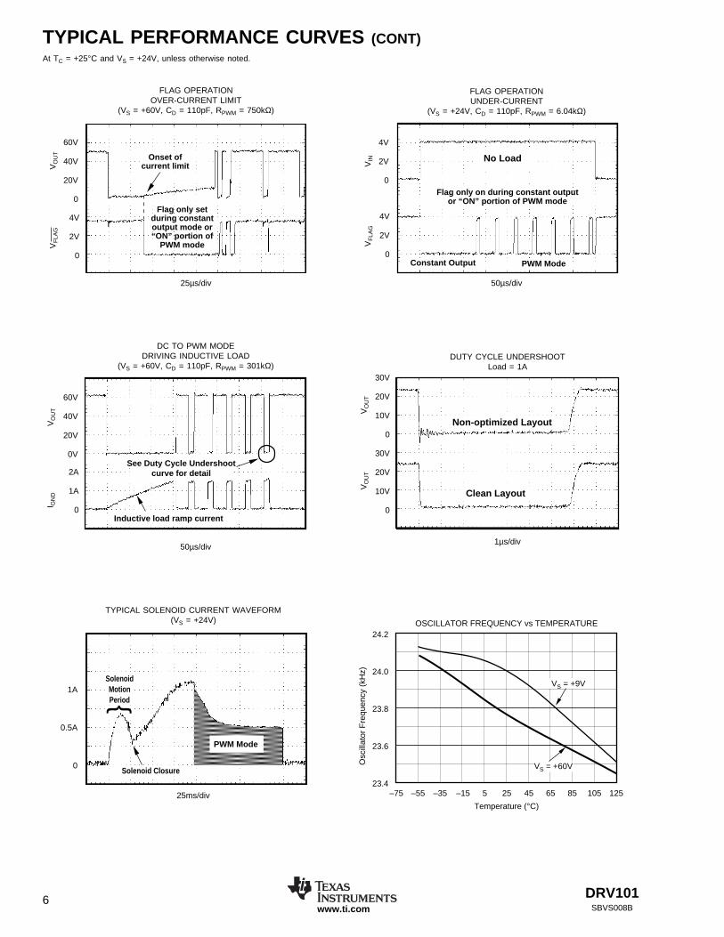
TYPICAL PERFORMANCE CURVES (CONT)At TC = +25°C and VS = +24V, unless otherwise noted.
VO
UT
FLAG OPERATIONOVER-CURRENT LIMIT
(VS = +60V, CD = 110pF, RPWM = 750kΩ)
FLAG OPERATIONUNDER-CURRENT
(VS = +24V, CD = 110pF, RPWM = 6.04kΩ)
No Load
2A
1A
0
VO
UT
DUTY CYCLE UNDERSHOOTLoad = 1A
DC TO PWM MODEDRIVING INDUCTIVE LOAD
(VS = +60V, CD = 110pF, RPWM = 301kΩ)30V
20V
10V
0
30V
20V
10V
0
VO
UT
TYPICAL SOLENOID CURRENT WAVEFORM(VS = +24V)
50µs/div
Inductive load ramp current
See Duty Cycle Undershootcurve for detail
25µs/div
60V
40V
20V
0V
I GN
D
1µs/div
PWM ModeConstant Output
Flag only on during constant outputor “ ON” portion of PWM mode
4V
2V
0
4V
2V
0
VIN
VF
LAG
50µs/div
1A
0.5A
0
25ms/div
PWM Mode
OSCILLATOR FREQUENCY vs TEMPERATURE
–75 –55 –35 –15 5 25 45 65 85 105 125
Temperature (°C)
Osc
illat
or F
requ
ency
(kH
z)
24.2
24.0
23.8
23.6
23.4
VS = +9V
VS = +60V
60V
40V
20V
0
4V
2V
0
VF
LAG
Onset ofcurrent limit
Flag only setduring constantoutput mode or“ ON” portion of
PWM mode
Clean Layout
Non-optimized Layout
VO
UT
Solenoid Closure
SolenoidMotionPeriod

DRV101 7SBVS008B www.ti.com
TYPICAL PERFORMANCE CURVES (CONT)At TC = +25°C and VS = +24V, unless otherwise noted.
MINIMUM DELAY TO PWM vs TEMPERATURE
–75 –50 –25 0 25 50 75 100 125
Temperature (°C)
Del
ay (
µs)
22
21
20
19
18
17
16
15
14
VS = +24V
No connection toDelay Adjust pin
(CD = 0)
VS = +60V
VS = +9V
NOMINAL DELAY TIME TO PWM vs TEMPERATURE
–75 –50 –25 0 25 50 75 100 125
Temperature (°C)
Del
ay (
ms)
104
102
100
98
96
94
92
90
88
VS = +9V
VS = +60V
VS = +24VVS = +24V
CD = 0.1µF

DRV1018SBVS008Bwww.ti.com
BASIC OPERATIONThe DRV101 is a low-side, bipolar power switch employinga pulse-width modulated (PWM) output for driving electro-mechanical and thermal devices. Its design is optimized fortwo types of applications; a two-state driver (open/close) forloads such as solenoids and actuators, and a linear driver forvalves, positioners, heaters, and lamps. Its wide supplyrange, adjustable delay to PWM mode, and adjustable dutycycle make it suitable for a wide range of applications.Figure 1 shows the basic circuit connections to operate theDRV101. A 0.1µF bypass capacitor is shown connected tothe power supply pin.
The Input (pin 1) is compatible with standard TTL levels.Input voltages between +2.2V and +5.5V turn the deviceoutput on, while pulling the pin low (0V to +1.2V), shuts theDRV101 output off. Input current is typically 80µA.
Delay Adjust (pin 2) and Duty Cycle Adjust (pin 3) allowexternal adjustment of the PWM output signal. The DelayAdjust pin can be left floating for minimum delay to PWMmode (typically 15µs) or a capacitor can be used to set thedelay time. Duty cycle of the PWM output can be controlled
FIGURE 1. Basic Circuit Connections and Timing Diagram.
by a resistor, analog voltage, or D/A converter. Figure 1bprovides an example timing diagram with the Delay Adjustpin connected to 0.1µF and duty cycle set for 25%. See the“Delay Adjust” and “Duty Cycle Adjust” text for equationsand further explanation.
Ground (pin 4) is electrically connected to the package tab.This pin must be connected to system ground for theDRV101 to function. This serves as the load current path toground, as well as the DRV101 reference ground.
The load (solenoid, valve, etc.) is connected between thesupply (pin 5) and output (pin 6). For an inductive load, anexternal diode across the output is required as shown inFigure 1a. The diode serves to maintain the hold force duringPWM operation. For remotely located loads, the externaldiode should be placed close to the DRV101 (Figure 1a). Theinternal clamp diode between the output and ground shouldnot be used to carry load current.
The Flag (pin 7) provides fault status for under-current,over-current, and thermal shutdown conditions. This pin isactive low with pin voltage typically +0.3V during a faultcondition. A small value capacitor may be needed betweenFlag and ground for noisy applications.
RPWMCD
DelayAdjust
Input
(TTL-Compatible)
On
Off
Thermal ShutdownOver/Under Current
Flag
Load
Duty Cycle Adjust
VS
24kHzOscillator
PWM
2 3
1
7 5
6
4
Gnd
Out
(electricallyconnected to
tab)
Delay
0.1µF
(a)
(b)
tP
tON
OUTPUTVS
0
INPUT
+2.2V to +5.5V
0V to +1.2V
Duty Cycle = = 25%tON
tP
RPWM = 130kΩ
tON ≈ 10.4µs
tP ≈ 41.6µs (1/24kHz)
Basic Circuit Connections
Simplified Timing DiagramCD = 0.1µF (95ms constant dc output before PWM)
RPWM = 130kΩ
(1)
NOTE: (1) External flyback diode required for inductive loads to conduct load current during the off cycle.For remotely located loads, diode should be placed close to the DRV101.
Motorola MSRS1100T3 (1A, 100V), MBRS360T3 (3A, 60V)
CD = 0.1µF95ms
• • •
• • •
Initial dc Output(set by value
of CD)
PWM Mode(resistor or voltage
controlled)

DRV101 9SBVS008B www.ti.com
APPLICATIONS INFORMATIONPOWER SUPPLY
The DRV101 operates from a single +9V to +60V supplywith excellent performance. Most behavior remains un-changed throughout the full operating voltage range. Param-eters which vary significantly with operating voltage areshown in the Typical Performance Curves.
ADJUSTABLE INITIAL 100% DUTY CYCLE
A unique feature of the DRV101 is its ability to provide aninitial constant dc output (100% duty cycle) and then switchto PWM mode to save power. This function is particularlyuseful when driving solenoids which have a much higherpull-in current requirement than hold requirement.
The duration of this constant dc output (before PWM outputbegins) can be externally controlled with a capacitor con-nected from Delay Adjust (pin 2) to ground according to thefollowing equation:
Delay Time ≈ CD • 106
(time in seconds, CD in Farads)
Leaving the Delay Adjust pin open results in a constantoutput time of approximately 15µs. The duration of thisinitial output can be reduced to less than 3µs by connectingthe pin to 5V. Table I provides examples of desired “delay”times (constant output before PWM mode) and the appropri-ate capacitor values or pin connection.
CONSTANT OUTPUT DURATION CD
3µs Pin connected to 5V15µs Pin open
100µs 100pF1ms 1nF
100ms 0.1µF
TABLE I. Delay Adjust Pin Connections.
ADJUSTABLE DUTY CYCLE
The DRV101’s externally adjustable duty cycle provides anaccurate means of controlling power delivered to the load.Duty cycle can be set from 10% to 100% with an externalresistor, analog voltage, or the output of a D/A converter.Reduced duty cycle results in reduced power dissipation.This keeps the DRV101 and load cooler, resulting in in-creased reliability for both devices. PWM frequency is aconstant 24kHz.
Resistor Controlled Duty Cycle
Duty cycle is easily programmed with a resistor (RPWM)connected between the Duty Cycle Adjust pin and ground.Increased resistor values correspond to decreased duty cycles.Table II provides resistor values for typical duty cycles.Resistor values for additional duty cycles can be obtainedfrom Figure 3. For reference purposes, the equation forcalculating RPWM is included in Figure 3.
FIGURE 3. RPWM vs Duty Cycle.FIGURE 2. Simplified Circuit Model of the Delay Adjust Pin.
The internal Delay Adjust circuitry is composed of a 3µAcurrent source and a 3V comparator as shown in Figure 2.Thus, when the pin voltage is less than 3V, the output deviceis 100% on (dc output mode).
3µA
2
CD
VS 3V Reference
Comparator
Delay Adjust
DRV101
RESISTOR(1) VOLTAGE(2)
DUTY CYCLE RPWM (kΩ) VPWM (V)
10 976 3.720 205 3.430 84.5 3.040 46.4 2.650 28.7 2.260 18.2 1.7570 11.8 1.3580 7.50 1.0090 4.87 0.75
NOTES: (1) Resistor values listed are nearest 1% standard values. (2) Do notdrive pin below 0.1V. For additional values, see “Duty Cycle vs Voltage” typicalperformance curve.
TABLE II. Duty Cycle Adjust. TA= +25°C, VS = +24V.
10 20 40 60 10080
Duty Cycle (%)
RP
WM
(kΩ
)
1000
100
10
1
RPWM = [ a + b (DC) + c (DC)2 + d (DC)3 + e (DC)4]–1
where: a = 2.4711 x 10⁻⁶
b = –5.2095 x 10⁻⁷
c = 4.4576 x 10⁻⁸
d = –7.6427 x 10⁻¹⁰
e = 6.8039 x 10⁻¹²
RPWM = [2.4711 x 10⁻⁶ + (–5.2095 x 10⁻⁷) (50) + (4.4576 x 10⁻⁸) (50)2
+ (–7.6427 x 10⁻¹⁰) (50)3 + (6.8039 x 10⁻¹²) (50)4]–1
DC = duty cycle in %
For 50% duty cycle:
= 28.7kΩ

DRV10110SBVS008Bwww.ti.com
Voltage Controlled Duty Cycle
Duty cycle can also be programmed with an analog voltage,VPWM. With VPWM ≈ 0.75V, duty cycle is near 90%. Increas-ing this voltage results in decreased duty cycles. Table IIprovides VPWM values for typical duty cycles. See the “DutyCycle vs Voltage” Typical Performance Curve for addi-tional duty cycles.
The Duty Cycle Adjust pin should not be driven below 0.1V.If the voltage source used can go between 0.1V and ground,a series resistor between the voltage source and the DutyCycle Adjust pin (Figure 4) is required to limit swing. If thepin is driven below 0.1V, the output will be unpredictable.
FIGURE 5. Simplified Circuit Model of the Duty CycleAdjust Pin.
STATUS FLAG
Flag (pin 7) provides fault indication for under-current,over-current, and thermal shutdown conditions. During afault condition, Flag output is driven low (pin voltagetypically drops to 0.3V). A pull-up resistor, as shown inFigure 6, is required to interface with standard logic. A smallvalue capacitor may be needed between Flag and ground innoisy applications.
Figure 6 gives an example of a non-latching fault monitoringcircuit, while Figure 7 provides a latching version. The Flagpin can sink several milliamps, sufficent to drive externallogic circuitry or an LED (Figure 8) to indicate when a faulthas occurred. In addition, the Flag pin can be used to turn offother DRV101’s in a system for chain fault protection.
The DRV101’s internal 24kHz oscillator sets the PWMperiod. This frequency is not externally adjustable. DutyCycle Adjust (pin 3) is internally driven by a 200µA currentsource and connects to the input of a comparator and a 19kΩresistor as shown in Figure 5. The DRV101’s PWM controldesign is inherently monotonic. That is, a decreased voltage(or resistor value) always produces an increased duty cycle.
200µA
3
VS
Comparator
Duty CycleAdjust
DRV101
19kΩ
Resistor orVoltage Source(1)
NOTE: (1) Do not drive pin below 0.1V.
3.8V
0.7V
f = 24kHz
FIGURE 4. Using a Voltage to Program Duty Cycle.
DRV101
D/AConverter(or analogvoltage)1kΩ(1)
PWM
VPWM
VS
3
4
6
5
Out
NOTE: (1) Required if voltage source can go below 0.1V.
DRV101
Thermal ShutdownOver/Under Current
4
6
7
Out
5kΩPull-Up
+5V
Flag
TTL or HCT
FIGURE 7. Latching Fault Monitoring Circuit.
FIGURE 6. Non-Latching Fault Monitoring Circuit.
DRV101
Thermal ShutdownOver/Under Current
4
6
7
Out
20kΩ
+5V
Flag
Q
Q
CLR
Flag
Flag
Flag Reset
J
CLK
GND K
VS
74XX76A
(1)
NOTE: (1) Small capacitor (10pF) may be required in noisy environments.
DRV101 11SBVS008B www.ti.com
An under-current fault occurs when the output current isbelow the under-scale current threshold (typically 23mA).For example, this function indicates when the load is discon-nected. Again, the flag output is not latched, so an under-current condition during PWM mode will produce a flagoutput that is modulated by the PWM waveform. An initial,brief under-current flag normally appears driving inductiveloads and may be avoided by adding a parallel resistorsufficient to move the initial current above the under-currentthreshold. An under-current flag may not appear for casetemperatures above 100°C. Avoid adding capacitance to pin6 (Out) as it may cause momentary current limiting.
Over-Temperature Fault
A thermal fault occurs when the die reaches approximately165°C, producing a similar effect as pulling the input low.Internal shutdown circuitry disables the output and resets theDelay Adjust pin. The Flag is latched in the low state (faultcondition) until the die has cooled to approximately 150°C.A thermal fault can occur in any mode of operation. Recov-ery from thermal fault will start in delay mode (constant dcoutput).
PACKAGE MOUNTING
Figure 9 provides recommended PCB layouts for both theTO-220 and DDPAK power packages. The tab of bothpackages is electrically connected to ground (pin 4). It maybe desirable to isolate the tab of TO-220 package from itsmounting surface with a mica (or other film) insulator (see
FIGURE 9. TO-220 and DDPAK Solder Footprints.
7-Lead DDPAK(1)
KTW Package(2)7-Lead TO-220KVT Package(2)
For improved thermal performance increase footprint area.See Figure 11, Thermal Resistance vs Circuit Board Copper Area.Refer to the mechanical drawings at the end of this document.
NOTES:(1)
(2)
Mean dimensions in inches. Refer to end of data sheetfor tolerances and detailed package drawings.
0.33
5
0.15
0.05
0.45
0.51
0.1050.05
0.035
0.04
0.2
0.08
5
Over/Under Current Fault
An over-current fault occurs when the output current isgreater than approximately 2.3A. The status flag is notlatched. Since current during PWM mode is switched on andoff, the flag output will be modulated with PWM timing (seeflag waveforms in the Typical Performance Curves).
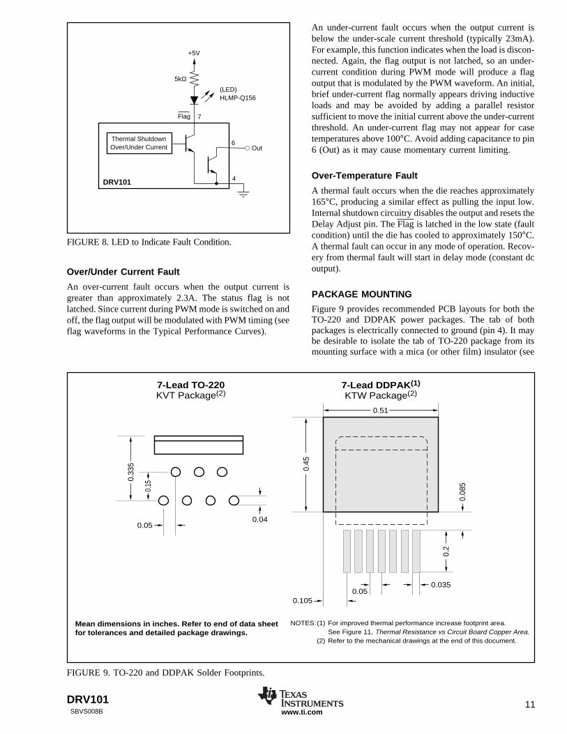
FIGURE 8. LED to Indicate Fault Condition.
DRV101
Thermal ShutdownOver/Under Current
4
6
7
Out
5kΩ
+5V
Flag
(LED)HLMP-Q156

DRV10112SBVS008Bwww.ti.com
Figure 10). For lowest overall thermal resistance, it is best toisolate the entire heat sink/DRV101 structure from themounting surface rather than to use an insulator between thesemiconductor and heat sink.
For best thermal performance, the tab of the DDPAK sur-face-mount version should be soldered directly to a circuitboard copper area. Increasing the copper area improves heatdissipation. Figure 11 shows typical thermal resistance fromjunction-to-ambient as a function of the copper area.
POWER DISSIPATION
Power dissipation depends on power supply, signal, and loadconditions. Power dissipation is equal to the product ofoutput current times the voltage across the conducting out-put transistor times the duty cycle. Power dissipation can beminimized by using the lowest possible duty cycle necessaryto assure the required hold force.
Application Bulletin AB-039 explains how to calculate ormeasure power dissipation with unusual signals and loads.
THERMAL PROTECTION
Power dissipated in the DRV101 will cause the junctiontemperature to rise. The DRV101 has thermal shutdowncircuitry that protects the device from damage. The thermal
protection circuitry disables the output when the junctiontemperature reaches approximately +165°C, allowing thedevice to cool. When the junction temperature cools toapproximately +150°C, the output circuitry is again enabled.Depending on load and signal conditions, the thermal protec-tion circuit may cycle on and off. This limits the dissipationof the amplifier but may have an undesirable effect on theload.
Any tendency to activate the thermal protection circuitindicates excessive power dissipation or an inadequate heatsink. For reliable operation, junction temperature should belimited to +125°C, maximum. To estimate the margin ofsafety in a complete design (including heat sink), increasethe ambient temperature until the thermal protection istriggered. Use worst-case load and signal conditions. Forgood reliability, thermal protection should trigger more than40°C above the maximum expected ambient condition ofyour application. This produces a junction temperature of125°C at the maximum expected ambient condition.
The internal protection circuitry of the DRV101 was de-signed to protect against overload conditions. It was notintended to replace proper heat sinking. Continuously run-ning the DRV101 into thermal shutdown will degrade reli-ability.
FIGURE 11. DDPAK Thermal Resistance vs Circuit Board Copper Area.
FIGURE 10. TO-220 Thermal Resistance vs Aluminum Plate Area.
0 1 2 3 4 5 6 7 8
18
16
14
12
10
8
The
rmal
Res
ista
nce
JA (
°C/W
)
Aluminum Plate Area (inches2)
THERMAL RESISTANCEvs ALUMINUM PLATE AREA
Aluminum Plate Area
Flat, RectangularAluminum Plate
DRV101TO-220 Package
θ
0.030in Al
0.062in Al
0.050in Al
Vertically Mountedin Free Air
Optional mica or film insulatorfor electrical isolation. Addsapproximately 1°C/W.
AluminumPlate Thickness
THERMAL RESISTANCE vs CIRCUIT BOARD COPPER AREA
50
40
30
20
10
0
The
rmal
Res
ista
nce,
θJA
(°C
/W)
0 1 2 3 4 5
Copper Area (inches2)
DRV101DDPAK
Surface-Mount Package1oz. copper
Circuit Board Copper Area
DRV101DDPAK
Surface-Mount Package

DRV101 13SBVS008B www.ti.com
Heat Sink Selection Example
A TO-220 package is dissipating 5 Watts. The maximumexpected ambient temperature is 35°C. Find the proper heatsink to keep the junction temperature below 125°C.
Combining Equations 1 and 2 gives:
TJ = TA + PD(θJC + θCH + θHA) (3)
TJ, TA, and PD are given. θJC is provided in the specificationtable, 3°C/W. θCH can be obtained from the heat sinkmanufacturer. Its value depends on heat sink size, area, andmaterial used. Semiconductor package type, mounting screwtorque, insulating material used (if any), and thermaljoint compound used (if any) also affect θCH. A typical θCHfor a TO-220 mounted package is 1°C/W. Now we can solvefor θHA:
(4)
To maintain junction temperature below 125°C, the heatsink selected must have a θHA less than 14°C/W. In otherwords, the heat sink temperature rise above ambient must beless than 70°C (14°C/W x 5W). For example, at 5 WattsThermalloy model number 6030B has a heat sinktemperature rise of 66°C above ambient (θHA = 66°C/5W =13.2°C/W), which is below the 70°C required in this ex-ample. Figure 12 shows power dissipation versus ambienttemperature for a TO-220 package with a 6030B heat sink.
Another variable to consider is natural convection versusforced convection air flow. Forced-air cooling by a small fancan lower θCA (θCH + θHA) dramatically. Heat sink manufac-turers provide thermal data for both of these cases. Foradditional information on determining heat sink require-ments, consult Application Bulletin AB-038.
As mentioned earlier, once a heat sink has been selected, thecomplete design should be tested under worst-case load andsignal conditions to ensure proper thermal protection.
HEAT SINKING
Most applications will not require a heat sink to assure thatthe maximum operating junction temperature (125°C) is notexceeded. However, junction temperature should be kept aslow as possible for increased reliability. Junction tempera-ture can be determined according to the equation:
TJ = TA + PDθJA (1)
where, θJA = θJC + θCH + θHA (2)
TJ = Junction Temperature (°C)
TA = Ambient Temperature (°C)PD = Power Dissipated (W)
θJC = Junction-to-Case Thermal Resistance (°C/W)
θCH = Case-to-Heat Sink Thermal Resistance (°C/W)θHA = Heat Sink-to-Ambient Thermal Resistance (°C/W)
θJA = Junction-to-Air Thermal Resistance (°C/W)
Figure 12 shows maximum power dissipation versus ambi-ent temperature with and without the use of a heat sink.Using a heat sink significantly increases the maximumpower dissipation at a given ambient temperature as shown.
FIGURE 12. Maximum Power Dissipation vs AmbientTemperature.
The difficulty in selecting the heat sink required lies indetermining the power dissipated by the DRV101. For dcoutput into a purely resistive load, power dissipation is simplythe load current times the voltage developed across theconducting output transistor times the duty cycle. Other loadsare not as simple. Consult Application Bulletin AB-039 forfurther insight on calculating power dissipation. Once powerdissipation for an application is known, the proper heat sinkcan be selected.
θHA = TJ – TA
PD
– θJC + θCH( )
θHA = 125°C – 35°C5W
– 3°C/W +1°C/W( ) = 14°C/W
10
8
6
4
2
0
Pow
er D
issi
patio
n (W
atts
)
0 25 50 75 100 125
Ambient Temperature (°C)
MAXIMUM POWER DISSIPATIONvs AMBIENT TEMPERATURE
TO-220 with Thermalloy6030B Heat Sink JA = 16.7°C/W
PD = (TJ (max) – TA) / JATJ (max) = 125°C
With infinite heat sink( JA = 3°C/W),max PD = 33Wat TA = 25°C
θ
θ
DDPAK
JA = 26°C/W(3 in2 one ozcopper mounting pad)
θ
DDPAK or TO-220
JA = 65°C/W (no heat sink)θ
θ
DRV10114SBVS008Bwww.ti.com
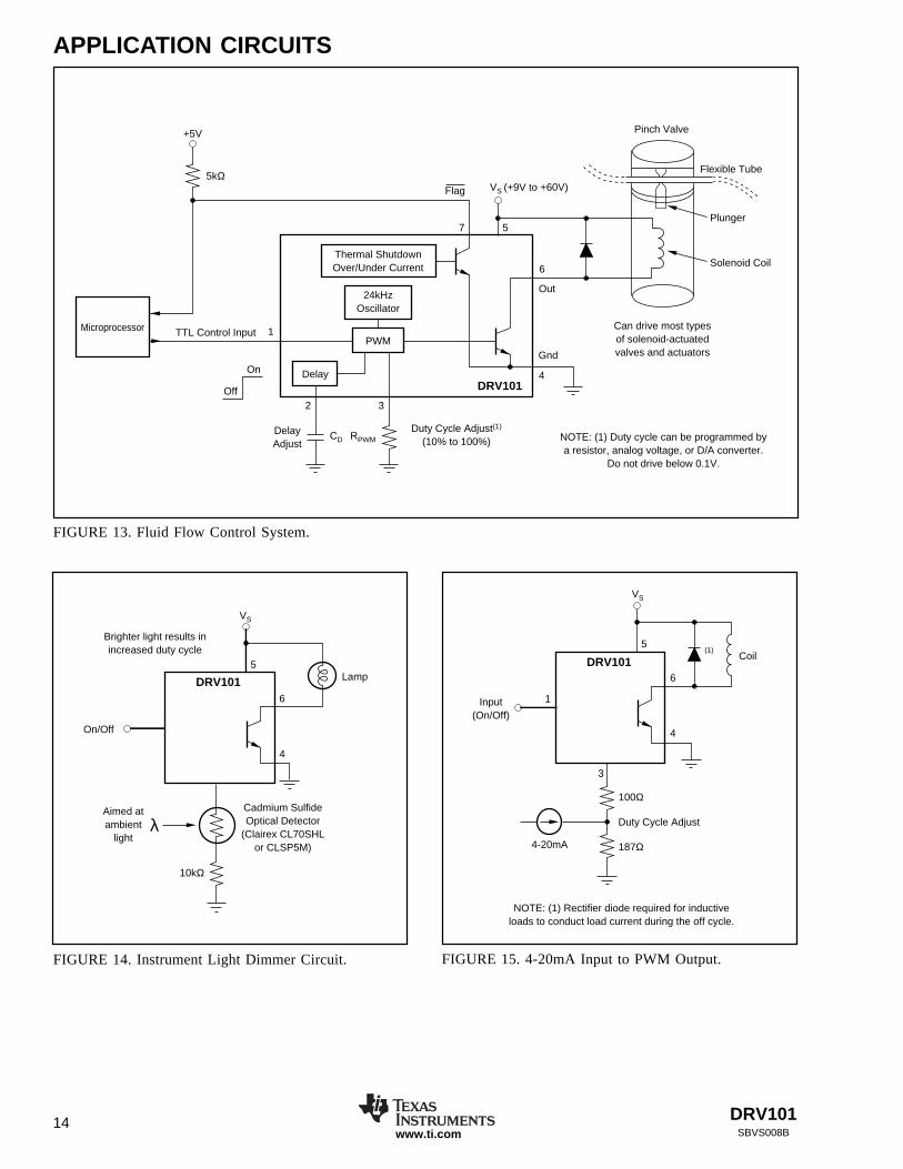
APPLICATION CIRCUITS
FIGURE 13. Fluid Flow Control System.
DRV101
Thermal ShutdownOver/Under Current
24kHzOscillator
PWM
Delay
Gnd
TTL Control Input
Off
On
Flexible Tube
Plunger
Pinch Valve
Solenoid Coil
Out
6
4
57
2
1
CD RPWM
3
VS (+9V to +60V)Flag
DelayAdjust
Duty Cycle Adjust(1)
(10% to 100%)
Can drive most typesof solenoid-actuatedvalves and actuators
NOTE: (1) Duty cycle can be programmed bya resistor, analog voltage, or D/A converter.
Do not drive below 0.1V.
Microprocessor
+5V
5kΩ
FIGURE 14. Instrument Light Dimmer Circuit. FIGURE 15. 4-20mA Input to PWM Output.
DRV101 Coil
Duty Cycle Adjust
Input(On/Off)
5
VS
6
4
1
3
4-20mA
NOTE: (1) Rectifier diode required for inductiveloads to conduct load current during the off cycle.
(1)
100Ω
187Ω
DRV101 Lamp
Cadmium SulfideOptical Detector
(Clairex CL70SHLor CLSP5M)
Aimed atambient
light
On/Off
λ
Brighter light results inincreased duty cycle
5
6
4
10kΩ
VS

DRV101 15SBVS008B www.ti.com
FIGURE 16. Temperature Controller.
DRV101
VS
On/Off
On/Off
Heating Element
Thermistor
Duty CycleAdjust
(a)
(b)
Higher temperature results in lower duty cycle
5
1
3
6
4
DRV101
REF200VS
VS
HeatingElement
Duty CycleAdjust
5
1
32
NC
6
1 2
4
0.1µF
0.1µF
2µF Film
72
3
4
6
10µF
100µA 100µA
1kΩ
10kΩ
10MΩ
OPA134
IN4148(1)
orThermistor
5kΩ at +25°C
20kΩ
4.7V
Integrator improves accuracy
NOTE: (1) Or any common silicon diode suitedto the mechanical mounting requirements.
TemperatureControl
7, 8
R1
R2
DRV10116SBVS008Bwww.ti.com
DRV101
dc Tachometer Coupled to Motor
T
+12V
5
6
4
R1 R2
Duty Cycle3
Speed Control(1)
M
NOTE: (1) Select R1/R2 ratio based on tachometer output voltage.
Input(On/Off)
1
FIGURE 17. Constant Speed Motor Control.
FIGURE 18. DC Motor Speed Control Using AC Tachometer.
One-Shot
–15V
5nFNP0
VFC32
0V to +10V
1kΩ
40kΩ
DRV101
2
DCMotor
Duty CycleAdjust
3
5
6
4
1
100kΩ
470kΩ
Frequency In
22kΩ
47kΩ10kΩ
M
TAC
Tachometer
Coupled to Motor
+40V
+15V
+15V
0.5µF
1nF
2N2222
Speed Control Input
VOUT
Delay Adjust
Open circuit willprovide 3.4V“on” signal

DRV101 17SBVS008B www.ti.com
FIGURE 19. Three-Phase Stepper Motor Driver Provides High-Stepping Torque.
DRV101
DRV101
DRV101
Phase 1StepperLogic In Phase 3
StepperLogic In
Phase 2StepperLogic In
+VSM
Only one DRV101 is turnedon at sequence time
DRV101 Lamp5
1
6
4
3
R2
VS = +9V to +60V
R1
R34.87kΩ
R44.87kΩ
C120µF
+
4.3VDIN5229
Duty Cycle Adjustafter soft start
Select R1 and R2 to dividedown VS to 5.5V max.
For example: with VS = 60VR1 = 11kΩ, R2 = 1kΩ
VS
VIN = • 60V = 5VSets start-up
duty cycle
1kΩ1kΩ + 11kΩ
FIGURE 20. Soft-Start Circuit for Incandescent Lamps and Other Sensitive Loads.

DRV10118SBVS008Bwww.ti.com
Load
5
6
4
20Ω(10W)DRV101
P-ChannelMOSFETIRF4905
12V70A
+12V
FIGURE 21. High Power, High-Side Driver.
FIGURE 22. High Power, Time Delay, Low-Side Driver.
FIGURE 23. Very High Power, Low-Side Driver.
120Ω(2W)750Ω
DRV101
N-ChannelIGBT
IRGPC50F
480V27A
2N3725A
2N3725AMPSA56
VS+12V
5
6
4
Load
NOTE: Duty cycle is inverted. For example, to achieve 25% duty cycle, program 75%.
Load12V50A
Out
5
1
6
4
32
12Ω(20W)1.4kΩ
1kΩ
DRV101N-ChannelMOSFETIRFZ48N
RPWM(2)CD
(1)
+12V
NOTES: (1) CD controls “OFF” time (turn-on delay). (2) Duty cycle is inverted.

DRV101 19SBVS008B www.ti.com
FIGURE 24. Isolated High-Side Driver.
Load
200Ω
RPWMCD
2.7kΩ
2kΩ
DRV101 P-ChannelMOSFETIRF9640
2N3725A
MPSA56
+170V
5
6
1
2 3
4ControlIn
0.1µF
0.1µF12V
+5V +
–
DCP010512
1
2
6
5
4N32Optocoupler

DRV10120SBVS008Bwww.ti.com
Revision History
DATE REVISION PAGE SECTION DESCRIPTION
1 Front Page Updated front page appearance.
11 Package Mounting Changed Figure 9 to show TI package designator.
NOTE: Page numbers for previous revisions may differ from page numbers in the current version.
5/09 B

PACKAGE OPTION ADDENDUM
www.ti.com 10-Apr-2013
Addendum-Page 1
PACKAGING INFORMATION
Orderable Device Status(1)
Package Type PackageDrawing
Pins PackageQty
Eco Plan(2)
Lead/Ball Finish MSL Peak Temp(3)
Op Temp (°C) Top-Side Markings(4)
Samples
DRV101F OBSOLETE DDPAK/TO-263
KTW 7 TBD Call TI Call TI
DRV101F/500 ACTIVE DDPAK/TO-263
KTW 7 500 Green (RoHS& no Sb/Br)
CU SN Level-2-260C-1 YEAR DRV101F
DRV101FKTWT ACTIVE DDPAK/TO-263
KTW 7 50 Green (RoHS& no Sb/Br)
CU SN Level-3-245C-168 HR DRV101F
DRV101FKTWTG3 ACTIVE DDPAK/TO-263
KTW 7 50 Green (RoHS& no Sb/Br)
CU SN Level-3-245C-168 HR DRV101F
DRV101T ACTIVE TO-220 KVT 7 50 Green (RoHS& no Sb/Br)
CU SN N / A for Pkg Type DRV101T
DRV101TG3 ACTIVE TO-220 KVT 7 50 Green (RoHS& no Sb/Br)
CU SN N / A for Pkg Type DRV101T
(1) The marketing status values are defined as follows:ACTIVE: Product device recommended for new designs.LIFEBUY: TI has announced that the device will be discontinued, and a lifetime-buy period is in effect.NRND: Not recommended for new designs. Device is in production to support existing customers, but TI does not recommend using this part in a new design.PREVIEW: Device has been announced but is not in production. Samples may or may not be available.OBSOLETE: TI has discontinued the production of the device.
(2) Eco Plan - The planned eco-friendly classification: Pb-Free (RoHS), Pb-Free (RoHS Exempt), or Green (RoHS & no Sb/Br) - please check http://www.ti.com/productcontent for the latest availabilityinformation and additional product content details.TBD: The Pb-Free/Green conversion plan has not been defined.Pb-Free (RoHS): TI's terms "Lead-Free" or "Pb-Free" mean semiconductor products that are compatible with the current RoHS requirements for all 6 substances, including the requirement thatlead not exceed 0.1% by weight in homogeneous materials. Where designed to be soldered at high temperatures, TI Pb-Free products are suitable for use in specified lead-free processes.Pb-Free (RoHS Exempt): This component has a RoHS exemption for either 1) lead-based flip-chip solder bumps used between the die and package, or 2) lead-based die adhesive used betweenthe die and leadframe. The component is otherwise considered Pb-Free (RoHS compatible) as defined above.Green (RoHS & no Sb/Br): TI defines "Green" to mean Pb-Free (RoHS compatible), and free of Bromine (Br) and Antimony (Sb) based flame retardants (Br or Sb do not exceed 0.1% by weightin homogeneous material)
(3) MSL, Peak Temp. -- The Moisture Sensitivity Level rating according to the JEDEC industry standard classifications, and peak solder temperature.
(4) Multiple Top-Side Markings will be inside parentheses. Only one Top-Side Marking contained in parentheses and separated by a "~" will appear on a device. If a line is indented then it is acontinuation of the previous line and the two combined represent the entire Top-Side Marking for that device.

PACKAGE OPTION ADDENDUM
www.ti.com 10-Apr-2013
Addendum-Page 2
Important Information and Disclaimer:The information provided on this page represents TI's knowledge and belief as of the date that it is provided. TI bases its knowledge and belief on informationprovided by third parties, and makes no representation or warranty as to the accuracy of such information. Efforts are underway to better integrate information from third parties. TI has taken andcontinues to take reasonable steps to provide representative and accurate information but may not have conducted destructive testing or chemical analysis on incoming materials and chemicals.TI and TI suppliers consider certain information to be proprietary, and thus CAS numbers and other limited information may not be available for release.
In no event shall TI's liability arising out of such information exceed the total purchase price of the TI part(s) at issue in this document sold by TI to Customer on an annual basis.
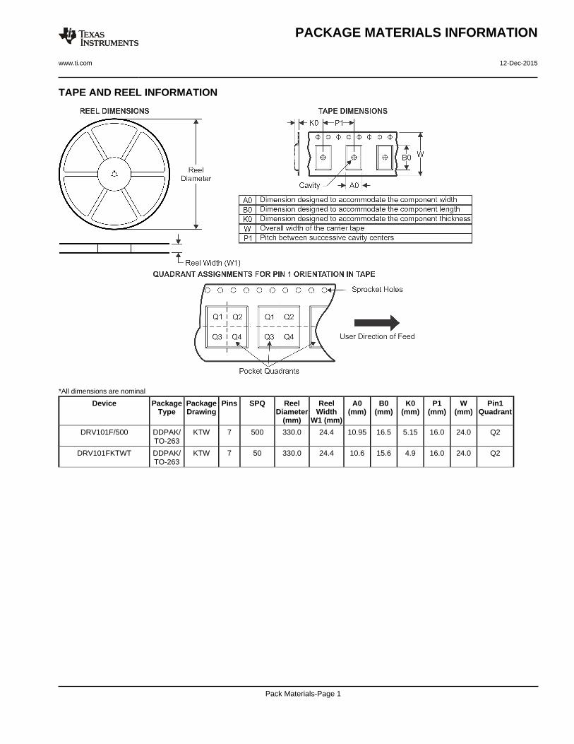
TAPE AND REEL INFORMATION
*All dimensions are nominal
Device PackageType
PackageDrawing
Pins SPQ ReelDiameter
(mm)
ReelWidth
W1 (mm)
A0(mm)
B0(mm)
K0(mm)
P1(mm)
W(mm)
Pin1Quadrant
DRV101F/500 DDPAK/TO-263
KTW 7 500 330.0 24.4 10.95 16.5 5.15 16.0 24.0 Q2
DRV101FKTWT DDPAK/TO-263
KTW 7 50 330.0 24.4 10.6 15.6 4.9 16.0 24.0 Q2
PACKAGE MATERIALS INFORMATION
www.ti.com 12-Dec-2015
Pack Materials-Page 1
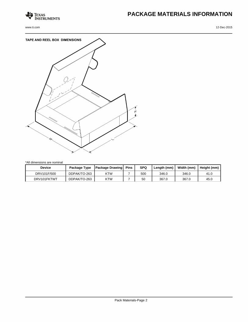
*All dimensions are nominal
Device Package Type Package Drawing Pins SPQ Length (mm) Width (mm) Height (mm)
DRV101F/500 DDPAK/TO-263 KTW 7 500 346.0 346.0 41.0
DRV101FKTWT DDPAK/TO-263 KTW 7 50 367.0 367.0 45.0
PACKAGE MATERIALS INFORMATION
www.ti.com 12-Dec-2015
Pack Materials-Page 2

MECHANICAL DATA
MPSF015 – AUGUST 2001
POST OFFICE BOX 655303 • DALLAS, TEXAS 75265
KTW (R-PSFM-G7) PLASTIC FLANGE-MOUNT
0.010 (0,25) A M
4201284/A 08/01
0.385 (9,78)0.410 (10,41)
M MB C
–A–0.006
–B–
0.170 (4,32)
0.183 (4,65)
0.000 (0,00)
0.012 (0,305)
0.104 (2,64)0.096 (2,44)
0.034 (0,86)0.022 (0,57)
0.050 (1,27)
0.055 (1,40)
0.045 (1,14)
0.014 (0,36)0.026 (0,66)
0.330 (8,38)
0.370 (9,40)
0.297 (7,54)0.303 (7,70)
0.0585 (1,485)
0.0625 (1,587)
0.595 (15,11)
0.605 (15,37)
0.019 (0,48)
0.017 (0,43)
0°~3°
0.179 (4,55)
0.187 (4,75)
0.056 (1,42)
0.064 (1,63)
0.296 (7,52)
0.304 (7,72)
0.300 (7,62)
0.252 (6,40)
F
C
C
H
H
H
C
A
NOTES: A. All linear dimensions are in inches (millimeters).B. This drawing is subject to change without notice.
C. Lead width and height dimensions apply to theplated lead.
D. Leads are not allowed above the Datum B.E. Stand–off height is measured from lead tip
with reference to Datum B.F. Lead width dimension does not include dambar
protrusion. Allowable dambar protrusion shall notcause the lead width to exceed the maximumdimension by more than 0.003”.
G. Cross–hatch indicates exposed metal surface.
H. Falls within JEDEC MO–169 with the exceptionof the dimensions indicated.


IMPORTANT NOTICE
Texas Instruments Incorporated and its subsidiaries (TI) reserve the right to make corrections, enhancements, improvements and otherchanges to its semiconductor products and services per JESD46, latest issue, and to discontinue any product or service per JESD48, latestissue. Buyers should obtain the latest relevant information before placing orders and should verify that such information is current andcomplete. All semiconductor products (also referred to herein as “components”) are sold subject to TI’s terms and conditions of salesupplied at the time of order acknowledgment.TI warrants performance of its components to the specifications applicable at the time of sale, in accordance with the warranty in TI’s termsand conditions of sale of semiconductor products. Testing and other quality control techniques are used to the extent TI deems necessaryto support this warranty. Except where mandated by applicable law, testing of all parameters of each component is not necessarilyperformed.TI assumes no liability for applications assistance or the design of Buyers’ products. Buyers are responsible for their products andapplications using TI components. To minimize the risks associated with Buyers’ products and applications, Buyers should provideadequate design and operating safeguards.TI does not warrant or represent that any license, either express or implied, is granted under any patent right, copyright, mask work right, orother intellectual property right relating to any combination, machine, or process in which TI components or services are used. Informationpublished by TI regarding third-party products or services does not constitute a license to use such products or services or a warranty orendorsement thereof. Use of such information may require a license from a third party under the patents or other intellectual property of thethird party, or a license from TI under the patents or other intellectual property of TI.Reproduction of significant portions of TI information in TI data books or data sheets is permissible only if reproduction is without alterationand is accompanied by all associated warranties, conditions, limitations, and notices. TI is not responsible or liable for such altereddocumentation. Information of third parties may be subject to additional restrictions.Resale of TI components or services with statements different from or beyond the parameters stated by TI for that component or servicevoids all express and any implied warranties for the associated TI component or service and is an unfair and deceptive business practice.TI is not responsible or liable for any such statements.Buyer acknowledges and agrees that it is solely responsible for compliance with all legal, regulatory and safety-related requirementsconcerning its products, and any use of TI components in its applications, notwithstanding any applications-related information or supportthat may be provided by TI. Buyer represents and agrees that it has all the necessary expertise to create and implement safeguards whichanticipate dangerous consequences of failures, monitor failures and their consequences, lessen the likelihood of failures that might causeharm and take appropriate remedial actions. Buyer will fully indemnify TI and its representatives against any damages arising out of the useof any TI components in safety-critical applications.In some cases, TI components may be promoted specifically to facilitate safety-related applications. With such components, TI’s goal is tohelp enable customers to design and create their own end-product solutions that meet applicable functional safety standards andrequirements. Nonetheless, such components are subject to these terms.No TI components are authorized for use in FDA Class III (or similar life-critical medical equipment) unless authorized officers of the partieshave executed a special agreement specifically governing such use.Only those TI components which TI has specifically designated as military grade or “enhanced plastic” are designed and intended for use inmilitary/aerospace applications or environments. Buyer acknowledges and agrees that any military or aerospace use of TI componentswhich have not been so designated is solely at the Buyer's risk, and that Buyer is solely responsible for compliance with all legal andregulatory requirements in connection with such use.TI has specifically designated certain components as meeting ISO/TS16949 requirements, mainly for automotive use. In any case of use ofnon-designated products, TI will not be responsible for any failure to meet ISO/TS16949.
Products ApplicationsAudio www.ti.com/audio Automotive and Transportation www.ti.com/automotiveAmplifiers amplifier.ti.com Communications and Telecom www.ti.com/communicationsData Converters dataconverter.ti.com Computers and Peripherals www.ti.com/computersDLP® Products www.dlp.com Consumer Electronics www.ti.com/consumer-appsDSP dsp.ti.com Energy and Lighting www.ti.com/energyClocks and Timers www.ti.com/clocks Industrial www.ti.com/industrialInterface interface.ti.com Medical www.ti.com/medicalLogic logic.ti.com Security www.ti.com/securityPower Mgmt power.ti.com Space, Avionics and Defense www.ti.com/space-avionics-defenseMicrocontrollers microcontroller.ti.com Video and Imaging www.ti.com/videoRFID www.ti-rfid.comOMAP Applications Processors www.ti.com/omap TI E2E Community e2e.ti.comWireless Connectivity www.ti.com/wirelessconnectivity
Mailing Address: Texas Instruments, Post Office Box 655303, Dallas, Texas 75265Copyright © 2015, Texas Instruments Incorporated