puttin pgas o wu tn ga work inork inork i nork in...
TRANSCRIPT

PP k nc entek, Inc. • One Park Way, Upper Saddle River, NJ 07458 • Tel: (201) 818-5900 • Fax: (201) 818-5904 • Email: [email protected] • http://www.pentek.com
11
PP e e nct , .entek, Inc.One Park Way, Upper Saddle River, New Jersey 07458
Tel: (201) 818-5900 • Fax: (201) 818-5904Email: [email protected] • http://www.pentek.com
Copyright © 2005, 2007, 2008, 2009, 2010, 2011, 2012 Pentek, Inc.Last Updated: August 2012
All rights reserved.Contents of this publication may not be reproduced in any form without written permission.
Specifications are subject to change without notice.Pentek, GateFlow, ReadyFow, SystemFlow and Cobalt are registered trademarks of Pentek, Inc.
TTech yn ogechnology
PGA FPGA R PGA FPGA Reso rcesourceso rcesesources
P oroducts
l np tioApplications
nkLinksknLinks
by
RRRRo g Hodger Hg Ho odger H. H k g. Hosking. H k g. HoskingVice-President & Cofounder of Pentek, Inc.
®
Puttin PGAs o WPutting FPGAs to Wu t n GA WP t i P s o Putting FPGAs to Work inork ino nrk iork inSoSofoSSoftware Rtware Rt re Rwa tware Rad o Syste sadio Systemsd y e sa o S stadio Systems
Sixth Edition

PP k nc entek, Inc. • One Park Way, Upper Saddle River, NJ 07458 • Tel: (201) 818-5900 • Fax: (201) 818-5904 • Email: [email protected] • http://www.pentek.com
22
Putting FPGAs to Work in Software Radio Systems
Preface
FPGAs have become an increasingly important resource for software radio systems. Programmable logic technology nowoffers significant advantages for implementing software radio functions such as DDCs (Digital Downconverters). Over the past
few years, the functions associated with DDCs have seen a shift from being delivered in ASICs (Application-Specific ICs) tooperating as IP (Intellectual Property) in FPGAs.
For many applications, this implementation shift brings advantages that include design flexibility, higher precisionprocessing, higher channel density, lower power, and lower cost per channel. With the advent of each new, higher-performance
FPGA family, these benefits continue to increase.
This handbook introduces the basics of FPGA technology and its relationship to SDR (Software Defined Radio) systems.A review of Pentek’s GateFlow FPGA Design Resources is followed by a discussion of features and benefits of FPGA-based DDCs.
Pentek SDR products that utilize FPGA technology and applications based on such products are also presented.
For a more in-depth discussion of SDR systems, the reader is referred to Pentek’s Software Defined Radio HandbookFor more information on complementary subjects, the reader is referred to these Pentek Handbooks:
Critical Techniques for High-Speed A/D Converters in Real-Time SystemsHigh-Speed Switched Serial Fabrics Improve System Design
High-Speed, Real-Time Recording Systems

PP k nc entek, Inc. • One Park Way, Upper Saddle River, NJ 07458 • Tel: (201) 818-5900 • Fax: (201) 818-5904 • Email: [email protected] • http://www.pentek.com
33
Putting FPGAs to Work in Software Radio Systems
DIGITAL
MIXER
DIGITAL
LOCAL
OSC
DSP
DDC
Digital Downconverter
RF
TUNER
Analog
IF Signal
Analog
RF SignalA/D
CONV
Digital IF
Samples LOWPASS
FILTER
Digital
Baseband
Samples
TT chn l gechnologyc n gh lechnology
TT Sc fc S fypical Sofypical Sof w e w e tware Rtware R d a mad madio Systemadio System SofSof r Ra ar Rtware Rtware R Ti i Tadio Tadio Taaasksasks
We begin our discussion with the basic elements ofa software radio receiver system.
The front end usually contains an analog RFamplifier and often an analog RF translator. Thistranslates the high frequency RF signals down to afrequency that an A/D converter can handle. This isusually below 200 MHz and is often an IF output.
The A/D output feeds the DDC (Digital Down-converter) stage, which is typically contained in a mono-lithic chip which forms the heart of a software radio system.
Notice, that after the signal is digitized by the A/Dconverter, all further operations are performed by digitalsignal processing hardware.
Here we’ve ranked some of the popular signalprocessing tasks associated with SDR systems on a twoaxis graph, with compute Processing Intensity on thevertical axis and Flexibility on the horizontal axis.
What we mean by process intensity is the degree ofhighly-repetitive and rather primitive operations. At theupper left are dedicated functions like A/D convertersand DDCs that require specialized hardware structuresto complete the operations in real time. ASICs are usuallychosen for these functions.
Flexibility pertains to the uniqueness or variabilityof the processing and how likely the function may haveto be changed or customized for any specific application.At the lower right are tasks like analysis and decision-making which are highly variable and often subjective.
Programmable general purpose processors or DSPsare usually chosen for these tasks since these tasks can beeasily changed by software.
Now let’s temporarily step away from the softwareradio tasks and take a deeper look at programmablelogic devices.
Figure 1 Figure 2

PP k nc entek, Inc. • One Park Way, Upper Saddle River, NJ 07458 • Tel: (201) 818-5900 • Fax: (201) 818-5904 • Email: [email protected] • http://www.pentek.com
44
Putting FPGAs to Work in Software Radio Systems
Early REarly Ro e o As P so es o P Asoles for FPGAsoles for FPGAs LL P g M d l g F G D e FPG D g Me d l gegacy FPGA Design Methodologiesegacy FPGA Design Methodologies
TT chn l gechnologyc n gh lechnology
As true programmable gate functions becameavailable in the 1970’s, they were used extensively byhardware engineers to replace control logic, registers,gates and state machines which otherwise would haverequired many discrete, dedicated ICs.
Often these programmable logic devices were one-time factory-programmed parts that were soldered downand never changed after the design went into production.
These programmable logic devices were mostly thedomain of hardware engineers and the software toolswere tailored to meet their needs. You had tools foraccepting boolean equations or even schematics to helpgenerate the interconnect pattern for the growingnumber of gates.
Then, programmable logic vendors started offeringpredefined logic blocks for flip-flops, registers andcounters, that gave the engineer a leg up on popularhardware functions.
Nevertheless, the hardware engineer was stillintimately involved with testing and evaluating thedesign using the same skills he needed for testingdiscrete logic designs. He had to worry about propaga-tion delays, loading, clocking and synchronizing—alltricky problems that usually had to be solved the hardway—with oscilloscopes or logic analyzers.
Figure 3 Figure 4
� Tools were oriented to hardware engineers
� Schematic processors
� Boolean processors
� Gates, registers, counters, multipliers
� Successful designs required high-level
hardware engineering skills for:
� Critical paths and propagation delays
� Pin assignment and pin locking
� Signal loading and drive capabilities
� Clock distribution
� Input signal synchronization and skew analysis
� Used primarily to replace discrete digital
hardware circuitry for:
� Control logic
� Glue logic
� Registers and gates
� State machines
� Counters and dividers
� Devices were selected by hardware engineers
� Programmed functions were seldom changed
after the design went into production

PP k nc entek, Inc. • One Park Way, Upper Saddle River, NJ 07458 • Tel: (201) 818-5900 • Fax: (201) 818-5904 • Email: [email protected] • http://www.pentek.com
55
Putting FPGAs to Work in Software Radio Systems
A : e c w A : w e c FPGAs: New Device TFPGAs: New Device T c no o yc no o yechnologyechnology A : e w nt A : w e nt FPGAs: New Development TFPGAs: New Development T lloolsools
TT chn l gechnologyc n gh lechnology
To support such powerful devices, new design toolsare appearing that now open up FPGAs to both hard-ware and software engineers. Instead of just acceptinglogic equations and schematics, these new tools acceptentire block diagrams as well as VHDL and Verilogdefinitions.
Choosing the best FPGA vendor often hingesheavily on the quality of the design tools available tosupport the parts.
Excellent simulation and modeling tools help toquickly analyze worst case propagation delays andsuggest alternate routing strategies to minimize themwithin the part. This minimizes some of the trickytiming work for hardware engineers and can save onehours of tedious troubleshooting during design verifica-tion and production testing.
In the last few years, a new industry of third partyIP (Intellectual Property) core vendors now offerthousands of application-specific algorithms. These areready to drop into the FPGA design process to help beatthe time-to-market crunch and to minimize risk.
Figure 5 Figure 6
� High Level Design Tools
� Block Diagram System Generators
� Schematic Processors
� High-level language compilers for
VHDL & Verilog
� Advanced simulation tools for modeling speed,
propagation delays, skew and board layout
� Faster compilers and simulators save time
� Graphically-oriented debugging tools
� IP (Intellectual Property) Cores
� FPGA vendors offer both free and licensed cores
� FPGA vendors promote third party core vendors
� Wide range of IP cores available
� 500+ MHz DSP Slices and Memory Structures
Over 3500 dedicated on-chip hardware multipliers
On-board GHz Serial Transceivers
Partial Reconfigurability Maintains
Operation During Changes
Switched Fabric Interface Engines
Over 690,000 Logic Cells
Gigabit Ethernet media access controllers
On-chip 405 PowerPC RISC micro-controller cores
Memory densities approaching 85 million bits
Reduced power with core voltages at 1 volt
Silicon geometries to 28 nanometers
High-density BGA and flip-chip packaging
Over 1200 user I/O pins
Configurable logic and I/O interface standards
�
�
�
�
�
�
�
�
�
�
�
�
�
�
It’s virtually impossible to keep up to date on FPGAtechnology, since new advancements are being madeevery day.
The hottest features are processor cores inside thechip, computation clocks to 500 MHz and above, andlower core voltages to keep power and heat down.
Several years ago, dedicated hardware multipliersstarted appearing and now you’ll find literally thousandsof them on-chip as part of the DSP initiative launchedby virtually all FPGA vendors.
High memory densities coupled with very flexiblememory structures meet a wide range of data flowstrategies. Logic slices with the equivalent of over tenmillion gates result from silicon geometries shrinkingbelow 0.1 micron.
BGA and flip-chip packages provide plenty of I/Opins to support on-board gigabit serial transceivers andother user-configurable system interfaces.
New announcements seem to be coming out everyday from chip vendors like Xilinx and Altera in a never-ending game of outperforming the competition.

PP k nc entek, Inc. • One Park Way, Upper Saddle River, NJ 07458 • Tel: (201) 818-5900 • Fax: (201) 818-5904 • Email: [email protected] • http://www.pentek.com
66
Putting FPGAs to Work in Software Radio Systems
F G f F G f FPGAs for SDRFPGAs for SDR P As th g P As g th FPGAs Bridge the SFPGAs Bridge the SDDDRDR ti l T l ti T Application T Application T as Ss S aask Spaceask Space
TT chn l gechnologyc n gh lechnology
As a result, FPGAs have significantly invaded theapplication task space as shown by the center bubble inthe task diagram above.
They offer the advantages of parallel hardware tohandle some of the high process intensity functions likeDDCs and the benefit of programmability to accommo-date some of the decoding and analysis functions of DSPs.
These advantages may come at the expense ofincreased power dissipation and increased product costs.However, these considerations are often secondary to theperformance and capabilities of these remarkable devices.
Like ASICs, all the logic elements in FPGAs canexecute in parallel. This includes the hardware multipli-ers, and you can now get over 500 of them on a singleFPGA.
This is in sharp contrast to programmable DSPs,which normally have just a handful of multipliers thatmust be operated sequentially.
FPGA memory can now be configured with thedesign tool to implement just the right structure fortasks that include dual port RAM, FIFOs, shift registersand other popular memory types.
These memories can be distributed along the signalpath or interspersed with the multipliers and mathblocks, so that the whole signal processing task operatesin parallel in a systolic pipelined fashion.
Again, this is dramatically different from sequentialexecution and data fetches from external memory as in aprogrammable DSP.
As we said, FPGAs now have specialized serial andparallel interfaces to match requirements for high- speedperipherals and buses.
Figure 7 Figure 8
� Parallel Processing
� Hardware Multipliers for DSP
� FPGAs can now have over 500 hardware multipliers
� Flexible Memory Structures
� Dual port RAM, FIFOs, shift registers, look up tables, etc.
� Parallel and Pipelined Data Flow
� Systolic simultaneous data movement
� Flexible I/O
� Supports a variety of devices, buses and interface standards
� High Speed
� Available IP cores optimized for special functions

PP k nc entek, Inc. • One Park Way, Upper Saddle River, NJ 07458 • Tel: (201) 818-5900 • Fax: (201) 818-5904 • Email: [email protected] • http://www.pentek.com
77
Putting FPGAs to Work in Software Radio Systems
RFPGA R RFPGA R r sesourcessresources
P P FPGA RFPGA R a s nc c a s nesource Comparisonesource Comparison
Figure 9
The above chart compares the available resources inthe five Xilinx FPGA families that are used in most ofthe Pentek products.
● Virtex-II Pro: VP50 and VP70● Virtex-4: FX, LX and SX● Virtex-5: LXT and SXT● Virtex-6: LXT and SXT● Virtex-7: 330T and 690T
The Virtex-II family includes hardware multipliersthat support digital filters, averagers, demodulatorsand FFTs—a major benefit for software radio signalprocessing. The Virtex-II Pro family dramaticallyincreased the number of hardware multipliers and alsoadded embedded PowerPC microcontrollers.
The Virtex-4 family is offered as three subfamiliesthat dramatically boost clock speeds and reduce powerdissipation over previous generations.
The Virtex-4 LX family delivers maximum logic andI/O pins while the SX family boasts of 512 DSP slicesfor maximum DSP performance. The FX family is agenerous mix of all resources and is the only family tooffer RocketIO, PowerPC cores, and the newly addedgigabit Ethenet ports.
*Virtex-II Pro and Virtex-4 Slices actually require 2.25 Logic Cells;*Virtex-5, Virtex-6 and Virtex-7 Slices actually require 6.4 Logic Cells
Vir t I -I tex-II P oro rVir 4etex-4 Virt -5tex-5 Vir etex-6 VVirttex-7 V 5 VP50, VP70 X, X SFX, LX, SX LXT , SXT XTLXT , SXT 03330T T 0, 690T
Logic Cells 53K–74K 41K–152K 46K–156K 128K–476K 326K–693KSlices* 24K–33K 18K–68K 7K–24K 20K–74K 51K–108KCLB Flip-Flops 47K–66K 51K–98K 33K–97K 160K–595K 408K–866KBlock RAM (kb) 4,176–5,904 4,176–6,768 4,752–8,784 9,504–36,304 27,000–52,920DSP Hard IP 18x18 Multipliers DSP48 DSP48E DSP48E DSP48EDSP Slices 232–328 96–512 128–640 480–2,016 1,120–3,600Serial Gbit Transceivers – 0–20 12–16 20–48 20–48PCI Express Support – – – Gen2x8 Gen2x8, Gen3x8SelectIO – 448–768 480–640 320–600 300–600
The Virtex-5 family LXT devices offer maximumlogic resources, gigabit serial transceivers, and Ethernetmedia access controllers. The SXT devices push DSPcapabilities with all of the same extras as the LXT.
The Virtex-5 devices offer lower power dissipation,faster clock speeds and enhanced logic slices. They alsoimprove the clocking features to handle faster memoryand gigabit interfaces. They support faster single-endedand differential parallel I/O buses to handle fasterperipheral devices.
The Virtex-6 and Virtex-7 devices offer still higherdensity, more processing power, lower power consump-tion, and updated interface features to match the latesttechnology I/O requirements including PCI Express.Virtex-6 supports PCIe 2.0 and Virtex-7 supports PCIe 3.0
The ample DSP slices are responsible for themajority of the processing power of the Virtex-6 andVirtex-7 families. Increases in operating speed from 500 MHzin V-4, to 550 MHz in V-5, to 600 MHz in V-6, to900 MHz in V-7 and continuously increasing densityallow more DSP slices to be included in the same-sizepackage. As shown in the chart, Virtex-6 tops out at animpressive 2,016 DSP slices, while Virtex-7 tops out atan even more impressive 3,600 DSP slices.

PP k nc entek, Inc. • One Park Way, Upper Saddle River, NJ 07458 • Tel: (201) 818-5900 • Fax: (201) 818-5904 • Email: [email protected] • http://www.pentek.com
88
Putting FPGAs to Work in Software Radio Systems
� Allows FPGA design engineers to easily add
functions to standard factory configuration
� Includes VHDL source code for all standard functions:
� Control and status registers
� A/D and Digital receiver interfaces
� Mezzanine interfaces
� Triggering, clocking, sync and gating functions
� Data packing and formatting
� Channel selection
� A/D / Receiver multiplexing
� Interrupt generation
� Data tagging and channel ID
� User Block for inserting custom code
Figure 10 Figure 11
a o A D e w e i Ra e ow A De i RGateFlow FPGA Design RGateFlow FPGA Design R rs u ss ur sesourcesesources a o e s n Ka e o s n KGateFlow FPGA Design KitGateFlow FPGA Design Kit
RA FPGA R re oesources
GateFlow
FPGA
Design
Kit
GateFlow
Factory
Installed
IP Cores
If you want to add your own algorithms to Pentekcatalog products, we offer the GateFlow FPGA DesignKit that includes VHDL source code for all the standardfactory functions.
VHDL is one of the most popular languages used inthe FPGA design tools. The GateFlow Design Kitincludes the VHDL source code for every softwaremodule we use to create these standard factory featuresof the product.
The standard factory configuration supports a widerange of operating modes, timing and sync functions, aswell as several different data formatting options.
This includes control and status registers, peripheralinterfaces, mezzanine interfaces, timing functions, dataformatting, channel selection, interrupt support, anddata tagging.
These are also fully supported with our ReadyFlowBoard Support Package.
GateFlow® is Pentek’s flagship collection of FPGADesign Resources. The GateFlow line is compatiblewith the Xilinx Virtex products and is available as twoseparate offerings:
If you want to add your own custom algorithms, weoffer the GateFlow FPGA Design Kit.
We also offer popular high-performance signal-process-ing algorithms with the GateFlow factory-installed IPCores. These algorithms are designed expressly for XilinxFPGAs and Pentek hardware products
Installed Cores are delivered to you preinstalled inyour Pentek FPGA-based product of choice and are fullysupported with Pentek ReadyFlow® Board SupportPackages.
Let’s start with the GateFlow FPGA Design Kit.

PP k nc entek, Inc. • One Park Way, Upper Saddle River, NJ 07458 • Tel: (201) 818-5900 • Fax: (201) 818-5904 • Email: [email protected] • http://www.pentek.com
99
Putting FPGAs to Work in Software Radio Systems
RA FPGA R re oesources
G D Co l t o A e i K f a y G t o A De i K f Co al y GateFlow FPGA Design Kit for Cobalt or Onyx PGateFlow FPGA Design Kit for Cobalt or Onyx P o cu to uctroductsroducts
Front Panel Interface
Memory
Controller
MemoryController
Sync Bus
Interface
PCI Express Interface
Global Registers
FLASH Interface
ClockGenerator
Timestamp
TestGenerator
PCI Express Backend
MemoryController
Memory
Controller
V-6 or V-7-
FPGA
User Application Container
Defined and
documented
interface signals
Board
RegistersUser
Registers
DMAs P14
LVDS
P16
MGTs
Factory Installed
Base Function Application
A/D & D/A Control
Data Packing & Formatting
Meta Data Files
Linked-List A/D Control
Linked-List D/A Control
Figure 12
The GateFlow FPGA Design Kit allows the user tomodify, replace and extend the standard factory-installedfunctions in the FPGA to incorporate special modes ofoperation, new control structures, and specialized signal-processing algorithms.
The Cobalt and Onyx architectures configure theFPGA with standard factory-supplied interfaces includingmemory controllers, DMA engines, A/D and D/Ainterfaces, timing and synchronization structures,triggering and gating logic, time stamping and headertagging, data formatting engines, and the PCIe interface.These resources are connected to the User ApplicationContainer using well-defined ports that present easy-to-usedata and control signals, effectively abstracting the lowerlevel details of the hardware.
Shown here is the FPGA block diagram of a typicalCobalt or Onyx module. The User Application Containerholds a collection of different factory-installed IPmodules connected to the various interfaces through thestandard ports surrounding the container. The specific IPmodules for each product are described in further detail inthe datasheet of that product.
The GateFlow Design Kit provides a completeXilinx ISE Foundation Tool project folder containingall the files necessary for the FPGA developer torecompile the entire project with or without anyrequired changes. VHDL source code for each IPmodule provides excellent examples of how the IPmodules work, how they might be modified, and howthey might be replaced with custom IP to implement aspecific function.

PP k nc entek, Inc. • One Park Way, Upper Saddle River, NJ 07458 • Tel: (201) 818-5900 • Fax: (201) 818-5904 • Email: [email protected] • http://www.pentek.com
10
Putting FPGAs to Work in Software Radio Systems
RA FPGA R re oesources
Figure 13
o G e gn l t r lo G e gn t r GateFlow FPGA Design Kit for Other GateFlow FPGA Design Kit for Other PP e e entek entek PP ttroductsroducts
The GateFlow FPGA Design Kit is intended for theprogramming of predefined user blocks located in the dataflow path specifically reserved for custom applications.These predefined blocks protect users from inadvertentlyaltering base functionality.
Pentek recommends user programming be limited tothe predefined user blocks to maintain base functional-ity. However, for more complex requirements, sufficientinformation is supplied in the kit for the user to modify,add to, or replace default board functions if necessary.Default configuration files are included with the DesignKit should it be necessary to restore standard factoryconfiguration.
Shown above is the block diagram of a typicalsoftware radio module. The diagram includes the FPGAand external hardware devices connected to it.
The blocks inside the FPGA are VHDL codemodules that handle the standard factory functions andinterfaces. The User Block is a VHDL module that sitsin the data path with pin definitions for input, output,status, control and clocks.
In the standard Design Kit product, the User Block isconfigured as a straight wire between the input and outputports. By creating a custom algorithm inside the block thatconforms to the pin definition, the user will have a low-riskexperience in recompiling and installing the custom code.Since Pentek provides source code for all the modules,changes outside the user block can also be made by theuser.
EXT
CLK
XTAL
OSC
LVDS
CLK &
SYNC
CLOCK
CONTROL
SYNC / GATE /
TRIGGER
GENERATOR
INTERRUPT
GENERATORSTATUS &
CONTROL
A/D
DIGITAL
RECEIVER
ANALOG
INPUT DATA
SELECT
DATA
FORMATTER
CLOCK
& SYNC
DRIVERS
MEZZANINE
INTERFACE

PP k nc entek, Inc. • One Park Way, Upper Saddle River, NJ 07458 • Tel: (201) 818-5900 • Fax: (201) 818-5904 • Email: [email protected] • http://www.pentek.com
11
Putting FPGAs to Work in Software Radio Systems
a o l d oe w r sa e ow l d or sGateFlow Installed IP CoresGateFlow Installed IP Cores
Figure 14
� Pentek Installs IP Cores in Pentek Products
� Cores are tailored and optimized for:
� Specific devices and I/O found on Pentek products
� Efficient FPGA resource utilization
� Execution and throughput speed
� Eliminates need for customer FPGA development
� Fully supported with ReadyFlow Board Support Libraries
Pentek is an AllianceCore Member, a third partyprogram sponsored by Xilinx for companies thatspecialize in specific areas of expertise in developingFPGA algorithms for niche application areas. Theseinclude image processing, communications, telecom,telemetry, signal intelligence, wireless communications,wireless networking, and many other disciplines.
Pentek offers popular high-performance signalprocessing algorithms installed in Pentek products. Thesealgorithms are designed expressly for Xilinx FPGAs andPentek harware products. The cores take full advantageof the numerous hardware multipliers to achieve highly-parallel processing structures that can dramaticallyoutperform programmable RISC and DSP processors.
Installed Cores are optimized for efficient FPGAresource utilization, execution and throughput speed.They are delivered to you preinstalled in your PentekFPGA-based product of choice and are fully tested andsupported with the Pentek ReadyFlow Board SupportPackages. Purchasing these popular factory-installedcores saves you the time and costs of acquiring FPGAtools and developing custom FPGA code.
RA FPGA R re oesources

PP k nc entek, Inc. • One Park Way, Upper Saddle River, NJ 07458 • Tel: (201) 818-5900 • Fax: (201) 818-5904 • Email: [email protected] • http://www.pentek.com
12
Putting FPGAs to Work in Software Radio Systems
Figure 15
t w o rt w o rDigital DownconverDigital Downconver ter Fter Fund alund alundamentalsundamentals
CICInitial
Downsample
CICCoarse Gain
CFIRPolyphaseDecimator
PFIRPolyphaseDecimator
Roundin
g
DDSNCO
Signal In
COMPLEXDIGITALMIXER I
Q
FilterCoefficients
Tuning Stage Data Reduction Gain Adjustment Additional Data Reductionand Signal Shaping
FilterCoefficients
SIN COS
TuningFrequency
Signal Out
Over the past few years, the functions associatedwith DDCs have seen a shift from being delivered inASICs (Application-Specific ICs) to operating as IP(Intellectual Property) in FPGAs.
For many applications, this implementation shiftbrings advantages that include: design flexibility, higherprecision processing, higher channel density, lowerpower, and lower cost per channel. With the advent ofeach new higher performance FPGA family during thepast few years, these benefits continue to increase.
To understand how FPGAs play a key role inimplementing DDCs that perform the function of areceiver, it’s important to break the DDC down into itsindividual functional blocks. The block diagram shows aclassic DDC. Regardless of whether it’s implemented inan ASIC or an FPGA, this is the common architectureof the DDC function.
The first stage of the DDC uses a complex digitalmixer to translate the frequency of interest down tobaseband. It uses a pair of multipliers and a DDS(Direct Digital Synthesizer) as the NCO (NumericallyControlled Oscillator). This function enables the user totune the receiver to the desired frequency of interest.The second stage of the DDC reduces the samplingfrequency of the signal to match the desired output
bandwidth. It uses a CIC (Cascaded Integrator Comb)filter to decimate the data.
A second CIC filter provides a coarse gain adjustmentstage. The signal is then passed to a pair of additionalpolyphase filters. First a CFIR (Compensation FiniteImpulse Response) filter then to a PFIR (ProgrammableFinite Impulse Response) filter. This filter pair providesadditional decimation and final signal shaping prior tothe rounding stage and final output.
When we get past all the acronyms, we realize thatmost of the individual function blocks of the DDC areimplemented using multipliers. It thus becomes appar-ent how the DDC might map into current FPGA families.Most new FPGAs include a wealth of DSP functionblocks which are primarily multipliers. The generalpurpose logic resource and on-chip memory of FPGAsalso match the requirements of the DDC for implement-ing the required FIR filters and filter coefficient tables.
As part of their IP library series, Xilinx provides afree DDC core. The core serves as a good generalreference design, following the classic DDC architectureshown here. While this core can be used as a buildingblock for general purpose DDCs, the real advantages ofan IP-based implementation can be best seen in optimizedcustom cores that are designed to match the requirementsof a specific application.
RA FPGA R re oesources

PP k nc entek, Inc. • One Park Way, Upper Saddle River, NJ 07458 • Tel: (201) 818-5900 • Fax: (201) 818-5904 • Email: [email protected] • http://www.pentek.com
13
Putting FPGAs to Work in Software Radio Systems
Pentek offers a series of high-performance IP-basedDDCs, available preinstalled in software radio modules.Each is optimized to match a specific range of applica-tion requirements.
These cores range from the high-channel count/narrowbandwidth of the 430 Core installed in the Model 7141,to the wider bandwidths and excellent SFDR (Spurious FreeDynamic Range) of the core installed in the Model 7153.
The above table lists some of the DDC cores availablefrom Pentek as software radio modules. For each core,pertinent specifications are listed. These products areavailable in industry standard PMC/XMC modules aswell as 3U and 6U CompactPCI, PCI, PCI Express andOpenVPX form factors. In addition to the IP-based
l s b o bl s oIP Enables SofIP Enables Sof r t a t ar tware Rtware R d a ad adio Padio P o co croductsroducts
DDC Number Decimation Input Rate SFDR Decimation Area per Power per Cost perImplementation of Channels Range (MHz) (dBFS) Steps Channel (mm2)1 Channel (W)2 Channel ($)3
TI GC4016 ASIC 4 32–16,384 160 115 1 72.3 0.25 41
Pentek 7141-420 2 2–64 110 118 Binary 612.5 2.5 204
Pentek 7141-430 256 1,024–9,984 110 110 256 4.7 0.01 2
Pentek 7142-428 4 2–65,536 125 108 1 206.2 2.0 102
Pentek 7151 256 128–1,024 200 105 64 4.7 0.04 6
Pentek 7152 32 16–8,192 200 105 8 38.3 0.25 44
Pentek 7153 4 2–256 200 120 1 206.2 1.25 29
Pentek 7153 2 2–65,536 200 120 1 612.5 2.5 57
Note 1 : Area per Channel = IC area ÷ number of channels.
Note 2 : GC4016 Power per Channel = Total IC power ÷ number of channels, IP Core Power per Channel = (FPGA power with IPcore – FPGA power without IP core) ÷ number of channels.
Note 3 : GC4016 Cost per Channel = cost of IC ÷ number of channels; IP core Cost per Channel = cost of FPGA resources used÷ number of channels.
Figure 16
solutions, a popular ASIC-based DDC solution from TexasInstruments, the GC4016, is included as a reference.
When compared on a size/power/cost per channelbasis, it becomes apparent that narrowband, highchannel-count DDC cores can be very efficientlyimplemented in FPGAs. Implementation of widebandDDCs consumes many more FPGA DSP and logicresources. As a result, the number of channels that canbe fit into a single FPGA is limited. Even with less cost-effective wideband DDCs, the custom IP approach cansometimes provide the only viable solution when aspecific performance characteristic is required. Theimproved SFDR of the Pentek 420 core is an example ofsuch a requirement.
RA FPGA R re oesources

PP k nc entek, Inc. • One Park Way, Upper Saddle River, NJ 07458 • Tel: (201) 818-5900 • Fax: (201) 818-5904 • Email: [email protected] • http://www.pentek.com
14
Putting FPGAs to Work in Software Radio Systems
An additional benefit of IP based solutions is theflexible nature of their implementation. The Models7141-420 and 7141-430 are created by using the samehardware base with different installed IP cores. Similarly,the Models 7151, 7152 and 7153 are all based on thesame 4-channel, 200 MHz, 16-bit A/D PMC/XMC withdifferent FPGA IP cores. All share the same software baseallowing migration between different applications to beaccomplished with minimum software porting.
Additionally, some applications like JTRS (JointTactical Radio System), need to operate across a wide
bl p m n ie t ne bl p m nt i nFlexible ImplementationFlexible Implementation
spectrum to handle the diverse signal types. Suchapplications can benefit greatly by IP based solutions.This Figure, shows the six optimized Pentek cores acrossa range of applications and the number of channels andbandwidth they typically require.
Again, this wide range of applications can besatisfied by using a small set of hardware with different,optimized IP cores. This is one of the fundamentalconcepts of SDR (Software Defined Radio), and it’sdifficult, if not impossible, to achieve with ASIC-basedsolutions.
Figure 17
RA FPGA R re oesources

PP k nc entek, Inc. • One Park Way, Upper Saddle River, NJ 07458 • Tel: (201) 818-5900 • Fax: (201) 818-5904 • Email: [email protected] • http://www.pentek.com
15
Putting FPGAs to Work in Software Radio Systems
Let’s now take a look at a complete receiver system.One common application is GSM 2G, a high channelcount, low bandwidth system. An E-GMS receiverrequires 174 channels spaced 200 kHz apart. Just threeor four years ago, a viable solution would have used theTI/Graychip 4-channel GC4016 ASIC-based DDCs.
A common board form factor for these types ofapplication is PMC, such as the Pentek Model 7131.One PMC can house two 100MHz A/Ds and fourGC4016s and all of the required interface and supportcircuitry. For a 174-channel system this would require11 Model 7131’s.
By comparison, an IP DDC with 174 channels andsimilar performance to the 4016 can fit in a singleVirtex-5 XC5VSX95T FPGA that can be housed in asingle PMC, along with four channels of 200MHz A/Dsand all support circuitry such as the Pentek Model7151. A visual comparison of these two solutions isshown in the above figure.
FPGAs continue to offer new possibilities andperformance when addressing processing tasks likedigital downconversion. With each new generation ofhigher performance FPGAs, processing precisioncontinues to increase. This enables IP-based DDCs tooutperform their ASIC-based cousins with specifica-tions like better SFDR.
As shown in this figure, it’s easy to understand howpacking many channels of DDCs into one or twoFPGAs can reduce the board count, power requirementsand cost over a solution that requires 30 or 40 individualASIC DDC chips. Additionally, FPGA solutions areextremely flexible since they can support vastly differentsignals with the simple loading of a different IP corewhile using the same hardware platform.
FPGA solutions are not a perfect match for allrequirements. They show the greatest advantages insystems with high channel densities and, typically,narrower bandwidths. In systems with just one or twochannels and bandwidths in the range of 100 MHz orgreater, the higher cost of the FPGAs needed canquickly exceed the cost of designing the system with asingle multichannel DDC ASIC. Again, while cost, sizeand power are important factors in designing a receiversystem, ultimately the technical requirements mayrequire the choice of an ASIC or FPGA solution.
m m System LSystem L ve a S sve Sa sevel Savingsevel Savings m r g a n A a m ar ng A a Comparing FPGAs and ASICsComparing FPGAs and ASICs
Figure 18 Figure 19
RA FPGA R re oesources

PP k nc entek, Inc. • One Park Way, Upper Saddle River, NJ 07458 • Tel: (201) 818-5900 • Fax: (201) 818-5904 • Email: [email protected] • http://www.pentek.com
16
Putting FPGAs to Work in Software Radio Systems
The Pentek family of board-level software radioproducts is the most comprehensive in the industry.Most of these products are available in several formatsto satisfy a wide range of requirements.
In addition to their commercial versions, manysoftware radio products are available in ruggedized andconduction-cooled versions.
All of the software radio products include input A/Dconverters. Some of these products are software radioreceivers in that they include only DDCs. Others aresoftware radio transceivers and they include DDCs aswell as DUCs with output D/A converters. These comewith independent input and output clocks.
All Pentek software radio products include multiboardsynchronization that facilitates the design of multichannelsystems with synchronous clocking, gating and triggering.
Pentek’s comprehensive software support includesthe ReadyFlow Board Support Package, the GateFlowFPGA Design Kit and high-performance factory-installed IP cores that expand the features and rangeof many Pentek software radio products. In addition,Pentek software radio recording systems are supportedwith SystemFlow® recording software that features agraphical user interface.
A complete listing of these products with activelinks to their datasheets on Pentek’s website is includedat the end of this handbook.
PP odu troductsodu troducts
Figure 20
P o P , P r s p nV X nd u M m c CI , P , a VMEb S fPM om c PCI, P , P r s p nV X, and VMEbu S fPMC, XMC, CompactPCI, PCI, PCI Express, OpenVPX, and VMEbus SofPMC, XMC, CompactPCI, PCI, PCI Express, OpenVPX, and VMEbus Sof Rw e w e Rtware Rtware R iiadioadio
PMC/XMC Module
6U CompactPCI Board
PCI BoardFull-length
PCI Express Board
Half-lengthPCI Express Board
VMEbus Board
3U OpenVPX BoardsCOTS and Rugged

PP k nc entek, Inc. • One Park Way, Upper Saddle River, NJ 07458 • Tel: (201) 818-5900 • Fax: (201) 818-5904 • Email: [email protected] • http://www.pentek.com
17
Putting FPGAs to Work in Software Radio Systems
Model 53313U VPX
M b ul i Mul ib Multiband RMultiband R c rc receiverseceivers
The unit supports the channel combining mode ofthe 4016s such that two or four individual 2.5 MHzchannels can be combined for output bandwidths of5 MHz or 10 MHz, respectively.
The sampling clock can be sourced from an internal100 MHz crystal oscillator or from an external clock suppliedthrough an SMA connector or the LVDS clock/sync bus onthe front panel. The LVDS bus allows multiple modules to besynchronized with the same sample clock, gating, triggeringand frequency switching signals. Up to 80 modules can besynchronized with the Model 9190 Clock and Sync Genera-tor. Custom interfaces can be implemented by using the 64user-defined FPGA I/O pins on the P4 connector.
Versions of the 7131 are also available as a PCIboard (Model 7631A), 6U cPCI (Models 7231 and7231D dual density), 3U cPCI (Model 7331) and 3UVPX (Model 5331). All these products have similarfeatures.
PP odu troductsodu troducts
The Model 7131, a 16-Channel Multiband Receiver,is a PMC module. The 7131 PMC may be attached to awide range of industry processor platforms equippedwith PMC sites.
Two 14-bit 105 MHz A/D Converters accepttransformer-coupled RF inputs through two front panelSMA connectors. Both inputs are connected to fourTI/GC4016 quad DDC chips, so that all 16 DDCchannels can independently select either A/D.
Four parallel outputs from the four DDCs deliverdata into the Virtex-II FPGA which can be either theXC2V1000 or XC2V3000. The outputs of the two A/Dconverters are also connected directly to the FPGA tosupport the DDC bypass path to the PCI bus and for directprocessing of the wideband A/D signals by the FPGA.
M d 7 1 Model 7131 PMC ●●●●● cPC e 3 Model 7231 6U cPCI ●●●●● l U 3 3 Model 7331 3U cPCI●●●●● o PC M d 7 1 Mod 7 1 PC Model 7631A PCI Model 7631A PCI ●●●●● o 3 M d 5 1 V Mod 5 1 3 V Model 5331 3U VPX Model 5331 3U VPX
Figure 21
Model 7231D6U cPCI
Model 73313U cPCI
Model 7631APCI
Model 7131PMC

PP k nc entek, Inc. • One Park Way, Upper Saddle River, NJ 07458 • Tel: (201) 818-5900 • Fax: (201) 818-5904 • Email: [email protected] • http://www.pentek.com
18
Putting FPGAs to Work in Software Radio Systems
1 5 MHz
I
1 5 MHz
I
TIMING BUS
GENERATOR A
XTL
OSC A
SYNC
INTERRUPTS
& CONTROL
TIMING BUS
GENERATOR B
XTL
OSC B
RF
XFORMR
RF
XFORMR
VIRTEX-II Pro FPGA
XC2VP50
DSP – Channelizer – Digital Delay – Demodulation – Decoding – Control – etc.
FLASH
16 MB
DDR
SDRAM
256 MB
DDR
SDRAM
128 MB
DDR
SDRAM
128 MBPCI 2.2 INTERFACE
(64 Bits / 66 MHz)
Sample
Clock B In
Sample
Clock A In
LVDS Clock A
LVDS Sync A
LVDS Gate A
TTL Gate/
Trigger
TTL Sync
LVDS Clock B
LVDS Sync B
LVDS Gate B
RF In RF In
Clock/Sync/Gate
Bus A
Clock/Sync/Gate
Bus B
To All
Sections Control/
Status
PCI BUS
(64 Bits / 66 MHz)
P15 XMC
VITA 42.0
(Serial RapidIO,
PCI-Express, etc.)
P4 PMC
FPGA I/O
(Option –104)
14 14
16
16
16
14
24
32
16
32 32 3264 64
RF XFORMR RF XFORMR
RF Out RF Out
DAC5686
DIGITAL UPCONVERTER
16-bit D/A 16-bit D/A
LTC2255
125 MHz
14-bit A/D
LTC2255
125 MHz
14-bit A/D
FRONT
PANEL
CONNECTOR
GC4016
4-CHANNEL
DDC
PP odu troductsodu troducts
Figure 22
The Model 7141 PMC/XMC module combinesboth receive and transmit capabilities with a high-performance Virtex II-Pro FPGA and supports theVITA 42 XMC standard with optional switched fabricinterfaces for high-speed I/O.
The front end of the module accepts two RF inputsand transformer-couples them into two 14-bit A/Dconverters running at 125 MHz. The digitized outputsignals pass to a Virtex-II Pro FPGA for signal process-ing or routing to other module resources.
These resources include a quad digital down-converter, a digital upconverter with dual D/A converters,512 MB DDR SDRAM delay memory and the PCIbus. The FPGA also serves as a control and statusengine with data and programming interfaces to each ofthe on-board resources. Factory-installed FPGA functionsinclude data multiplexing, channel selection, data packing,gating, triggering, and SDRAM memory control.
In addition to acting as a simple transceiver, themodule can perform user-defined DSP functions on the
baseband signals, developed using Pentek’s GateFlowand ReadyFlow development tools.
The module includes a TI/GC4016 quad digitaldownconverter along with a TI DAC5686 digitalupconverter with dual D/A converters.
Each channel in the downconverter can be set withan independent tuning frequency and bandwidth. Theupconverter translates a real or complex baseband signal toany IF center frequency from DC to 160 MHz and candeliver real or complex (I + Q) analog outputs throughits two 16-bit D/A converters. The digital upconvertercan be bypassed for two interpolated D/A outputs withsampling rates to 500 MHz.
Versions of the 7141 are also available as a PCIefull-length board (Models 7741 and 7741D dual density),PCIe half-length board (Model 7841), 3U VPX board(Model 5341), PCI board (Model 7641), 6U cPCI(Models 7241 and 7241D dual density), and 3U cPCI(Model 7341).
Model 7141-703 is a conduction-cooled version.
Model 7141PMC/XMC
u n a u an Multiband TMultiband T s ve in e h Vns e ve h Viransceivers with Virransceivers with Vir Pt I t I Ptex-II Ptex-II Pr F G r F Gro FPGAro FPGA
el 4 C Model 7141 PMC/XMC ●●●●● o 2 M d 6 Model 7241 6U cPCI ●●●●● M d 3 7 1 Model 7341 3U cPCI ● ● ● ● ● 6 IMod PCModel 7641 PCI●●●●● Mod 7 Model 7741 F o 7 M d Model 7741 F l t PCI ull-length PCIe l I t PC ull-length PCIe ●●●●● Mod 8 l th PCI Model 7841 Half-length PCIe Mod 8 CI l th P Model 7841 Half-length PCIe ●●●●● 5 1 3 PX Model 5341 3U VPX 3 5 1 PX Model 5341 3U VPX

PP k nc entek, Inc. • One Park Way, Upper Saddle River, NJ 07458 • Tel: (201) 818-5900 • Fax: (201) 818-5904 • Email: [email protected] • http://www.pentek.com
19
Putting FPGAs to Work in Software Radio Systems
PP odu troductsodu troducts
TT ns e ve u i h Wns e ve i h u Wransceivers with Dual Wransceivers with Dual W e a nt o a i n d p de a nt po a i n ideband DDC and Interpolation Fideband DDC and Interpolation F l r t l l r t l ilter Installed Coresilter Installed Cores
Figure 23
The Pentek IP Core 420 includes a dual high-performance wideband DDC and an interpolation filter.Factory-installed in the Model 7141 FPGA, they extendthe range of both the GC4016 ASIC DDC and theDAC5686 DUC.
Each of the core 420 DDCs translates any frequencyband within the input bandwidth range down to zerofrequency. A complex FIR low pass filter removes any out-of-band frequency components. An output decimator andformatter deliver either complex or real data. An input gainblock scales both I and Q data streams by a 16-bit gainterm.
The mixer utilizes four 18x18-bit multipliers tohandle the complex inputs from the NCO and thecomplex data input samples. The FIR filter is capable ofstoring and utilizing up to four independent sets of18-bit coefficients for each decimation value. Thesecoefficients are user-programmable by using RAMstructures within the FPGA.
The decimation settings of 2, 4, 8, 16, 32, and 64provide output bandwidths from 40 MHz down to 1.25MHz for an A/D sampling of 100 MHz. A multiplexer allowsdata to be sourced from either the A/Ds or the GC4016,extending the cascaded decimation range to 1,048,576.
The interpolation filter included in the 420 Core,expands the interpolation factor from 2 to 32,768programmable in steps of 2, and relieves the hostprocessor from performing upsampling tasks. Includingthe DUC, the maximum interpolation factor is 32,768which is comparable to the maximum decimation of theGC4016 narrowband DDC.
Versions of the 7141-420 are also available as a 3UVPX board (Model 5341-420), PCIe full-length board(Models 7741-420 and 7741D-420 dual density), PCIehalf-length board (Model 7841-420), PCI board (Model7641-420), 6U cPCI (Models 7241-420 and 7241D-420dual density), or 3U cPCI (Model 7341-420).Model 7141-703-420 is a conduction-cooled version.
RF
XFORMR
RF
XFORMR
RF
XFORMR
RF
XFORMR1 5 MHz
14-bit A/D
1 5 MHz
14-bit A/D
CLOCK &
SYNC
GENERATOR
XTAL
OSC A
XTAL
OSC B
MUX
GC4016 DIGITAL
DOWNCONVERTR
DAC 5686
DIGITAL
UPCONVERTER
16-bit
500 MHZ
D/A
16-bit
500 MHZ
D/A
128 MB DDR
SDRAM
128 MB DDR
SDRAM
256 MB DDR
SDRAM
PCI 2.2
INTERFACE
MEMORY
CONTROL
&
DATA ROUTING
MEM W
FIFO
MEM W
FIFO
A/D A
FIFO
A/D B
FIFO
DDC A
FIFO
DDC B
FIFO
DDC C
FIFO
DDC D
FIFO
D/A A
FIFO
D/A B
FIFO
MUX
MUX
CFIR
FILTER
CIC
FILTER
MUX
WIDEBAND
DIGITAL
DOWNCONVERTR A
DECIMATION: 2 – 64
WIDEBAND
DIGITAL
DOWNCONVERTR A
DECIMATION: 2 – 64
M
U
X
M
U
X
MUX
CH A
RF In
CH B
RF In
CH A
RF Out
CH B
RF Out
Sample
Clock A In
Clock/Sync
Bus
Sample
Clock B In
A B C D
A B C D
MEMORY
MEMORY
DDC C
DDC D
D/A A
D/A B
A/D A
A/D B
A/D A
A/D B
DDC A
DDC B
A/D A
A/D B
DDC A
DDC BWB DDC A
DDC A
WB DDC B
DDC B
MEMORY
D/A A FIFO
MEMORY
D/A B FIFO
PCI BUS
64 bit /
66 MHz
WIDEBAND DDC CORE
INTERPOLATION CORE
XC2VP50
RF
XFORMR
RF
XFORMR
RF
XFORMR
RF
XFORMR
LTC2255
125 MHz
14-bit A/D
LTC2255
125 MHz
14-bit A/D
CLOCK &
SYNC
GENERATOR
XTAL
OSC A
XTAL
OSC B
MUX
GC4016 DIGITAL
DOWNCONVERTR
DAC 5686
DIGITAL
UPCONVERTER
16-bit
500 MHZ
D/A
16-bit
500 MHZ
D/A
128 MB DDR
SDRAM
128 MB DDR
SDRAM
256 MB DDR
SDRAM
PCI 2.2
INTERFACE
e 7 1 2 l Model 7141-420 PMC/XMC ●●●●● o 4 M d 2 - U I Model 7241-420 6U cPCI ●●●●● l 2 4 Model 7341-420 3U cPCI 7 4 0 P Model 7641-420 PCI 4 7 0 P Model 7641-420 PCI ●●●●● 7 4 Model 7741-420 F 4 7 Model 7741-420 Fu len t Iull-length PCIeu t Ilen ull-length PCIe
el t IM - 2 l n eModel 7841-420 Half-length PCIe ●●●●● Mod 4 4 PX Model 5341-420 3U VPX

PP k nc entek, Inc. • One Park Way, Upper Saddle River, NJ 07458 • Tel: (201) 818-5900 • Fax: (201) 818-5904 • Email: [email protected] • http://www.pentek.com
20
Putting FPGAs to Work in Software Radio Systems
PP odu troductsodu troducts
TTTT r c w r c w ransceivers with 256-ransceivers with 256- h r w d D l o n D t h r w nd DD t l oChannel Narrowband DDC Installed CoreChannel Narrowband DDC Installed Core
Figure 24
For applications that require many channels ofnarrowband downconverters, Pentek offers the GateFlowIP Core 430 256-channel digital downconverter bank.Factory installed in the Model 7141 FPGA, Core 430creates a flexible, very high-channel count receiversystem in a small footprint.
Unlike classic channelizer methods, the Pentek 430core allows for completely independent programmabletuning of each individual channel with 32-bit resolutionas well as filter characteristics comparable to manyconventional ASIC DDCs.
Added flexibility comes from programmable globaldecimation settings ranging from 1024 to 8192 in stepsof 256, and 18-bit user programmable FIR decimatingfilter coefficients for the DDCs. Default DDC filtercoefficient sets are included with the core for all possibledecimation settings.
Core 430 utilizes a unique method of channelization.It differs from others in that the channel center frequen-
RF
XFORMR
RF
XFORMR
RF
XFORMR
RF
XFORMR1 5 MHz
14-bit A/D
1 5 MHz
14-bit A/D
CLOCK &
SYNC
GENERATOR
XTAL
OSC A
XTAL
OSC B
MUX
GC4016 DIGITAL
DOWNCONVERTR
DAC 5686
DIGITAL
UPCONVERTER
16-bit
500 MHZ
D/A
16-bit
500 MHZ
D/A
PCI 2.2
MEM W
FIFO
MEM W
FIFO
D/A A
FIFO
D/A B
FIFO
CH A
RF In
CH B
RF In
CH A
RF Out
CH B
RF Out
Sample
Clock A In
Clock/Sync
Bus
Sample
Clock B In
A B C D
A B C D
DDC 1
Local Oscillator, Mixer, Filter
M
U
X
1
MUX
M
U
X
DDC A
FIFO
DDC B
FIFO
DDC C
FIFO
DDC D
FIFO
OUT A
DDC A
OUT B
DDC B
OUT C
DDC C
OUT D
DDC D
PCI BUS
64 bit /
66 MHz
256 CHANNEL DIGITAL DOWNCONVERTER BANK
CORE
XC2VP50
RF
XFORMR
RF
XFORMR
RF
XFORMR
RF
XFORMR
LTC2255
125 MHz
14-bit A/D
LTC2255
125 MHz
14-bit A/D
CLOCK &
SYNC
GENERATOR
XTAL
OSC A
XTAL
OSC B
MUX
GC4016 DIGITAL
DOWNCONVERTR
DAC 5686
DIGITAL
UPCONVERTER
16-bit
500 MHZ
D/A
16-bit
500 MHZ
D/A
PCI 2.2
INTERFACE
DDC 1
Local Oscillator, Mixer, Filter
DDC 255
Local Oscillator, Mixer, Filter
DDC 256
Local Oscillator, Mixer, Filter
e 7 1 3 l Model 7141-430 PMC/XMC ●●●●● o 4 M d 2 - U I Model 7241-430 6U cPCI ●●●●● l 3 4 Model 7341-430 3U cPCI 7d 4Model 7641-43 C 0 PCI ●●●●● 4 7 Model 7741-43 0 F t u n Iull-length PCIe
M 4 7M 7 4Model 7841-4Model 7841-433 th I th I0 Half-length PCIe0 Half-length PCIe ●●●●● o M d 4 4 Mod 4 4 Model 5341-430 3U VPX Model 5341-430 3U VPX
cies need not be at fixed intervals, and are independentlyprogrammable to any value.
Core 430 DDC comes factory installed in the Model7141-430. A multiplexer allows data to be sourced from eitherA/D. At the output, a multiplexer allows for routing eitherthe output of the GC4016 or the 430 DDC to the PCI Bus.
In addition to the DDC outputs, data from bothA/D channels are presented to the PCI Bus at a rate equalto the A/D clock rate divided by any integer value between1 and 4096. A TI DAC5686 digital upconverter and dualD/A accepts baseband real or complex data streams fromthe PCI Bus with signal bandwidths up to 50 MHz.
Versions of the 7141-430 are also available as a PCIefull-length board (Models 7741-430 and 7741D-430 dualdensity), PCIe half-length board (Model 7841-430), 3UVPX board (Model 5341-430), PCI board (Model 7641-430), 6U cPCI (Models 7241-430 and 7241D-430 dualdensity), or 3U cPCI (Model 7341-430).Model 7141-703-430 is a conduction-cooled version.

PP k nc entek, Inc. • One Park Way, Upper Saddle River, NJ 07458 • Tel: (201) 818-5900 • Fax: (201) 818-5904 • Email: [email protected] • http://www.pentek.com
21
Putting FPGAs to Work in Software Radio Systems
DDR 2
SDRAM
256 MB
DDR 2
SDRAM
256 MB
DDR 2
SDRAM
256 MB
32 32 32
32
RF
XFORMR
RF Out
DAC5686
DIGITAL
UPCONVERTER
16-bit D/A
RF
XFORMR
LTC2255
125MHz
14-bit A/D
RF In
14
RF
XFORMR
LTC2255
125MHz
14-bit A/D
RF In
14
RF
XFORMR
LTC2255
125MHz
14-bit A/D
RF In
14
RF
XFORMR
LTC2255
125MHz
14-bit A/D
RF In
14
P15 XMC
VITA 42.0
P4 PMC
FPGA I/O
(Option –104)
64
64LOCAL
BUS
VIRTEX-4 FPGA
XC4VFX60 or XC4VFX100
PCI BUS
(64 Bits / 66 MHz)
PCI 2.2
INTERFACE
SERIAL
INTERFACE
32 32 32HI-SPEED
BUSES
VIRTEX-4 FPGA
XC4VSX55
DSP – Channelizer – Digital Delay – Demodulation – Decoding – Control – etc.
Control/
Status
TIMING BUS
GENERATOR A
XTL
OSC A
SYNC
INTERRUPTS
& CONTROL
TIMING BUS
GENERATOR B
XTL
OSC B
LVDS Clock A
LVDS Sync A
LVDS Gate A
TTL Gate/
Trigger
TTL Sync
LVDS Clock B
LVDS Sync B
LVDS Gate B
Clock/Sync/Gate
Bus A
Clock/Sync/Gate
Bus B
To All
Sections
Sample
Clock In
PP odu troductsodu troductsPP odu troductsodu troducts
Model 7142PMC/XMC
Figure 25
t c nne t c nne Multichannel TMultichannel T a t ri r a i r t rransceivers with Virransceivers with Vir Pe 4 se 4 P stex-4 FPGAstex-4 FPGAs
Mod 1Model 714o 1M d Model 7142222 C/XMC PMC/XMC / MC C X PMC/XMC ●●●●● 7 Model 724 7 Model 7242222 6 6U cPCI 6 6U cPCI ●●●●● M d 7 Model 734 M d 7 Model 7342222 3U 3U cPCI U 3 3U cPCI ●●●●● o l 6Model 764l o 6Model 76422 PCI PCI o M d Model 77744 F2 F el tull-length I PCIe ●●●●● Model 784 g l -l n h2 Half-length PCIe ●●●●● e Model 53422 U 3U VPXVPX
The Model 7142 is a Multichannel PMC/XMCmodule. It includes four 125 MHz 14-bit A/D convert-ers and one upconverter with a 500 MHz 16-bit D/Aconverter to support wideband receive and transmitcommunication channels.
Two Xilinx Virtex-4 FPGAs are included: anXC4VSX55 or LX100 and an XC4VFX60 or FX100.The first FPGA is used for control and signal processingfunctions, while the second one is used for implement-ing board interface functions including the XMC interface.
It also features 768 MB of SDRAM for implementingup to 2.0 sec of transient capture or digital delay memoryfor signal intelligence tracking applications at 125 MHz.
A 16 MB flash memory supports the boot code forthe two on-board IBM 405 PowerPC microcontrollercores within the FPGA.
A 9-channel DMA controller and 64 bit / 66 MHz PCIinterface assures efficient transfers to and from the module.
A high-performance 160 MHz IP core wideband digitaldownconverter may be factory-installed in the first FPGA.
Two 4X switched serial ports, implemented with theXilinx Rocket I/O interfaces, connect the second FPGAto the XMC connector with two 2.5 GB/sec data linksto the carrier board.
A dual bus system timing generator allows separateclocks, gates and synchronization signals for the A/Dand D/A converters. It also supports large, multichannelapplications where the relative phases must be preserved.
Versions of the 7142 are also available as a PCIe full-length board (Models 7742 and 7742D dual density),PCIe half-length board (Model 7842), 3U VPX (Model5342), PCI board (Model 7642), 6U cPCI (Models 7242and 7242D dual density), and 3U cPCI (Model 7342).

PP k nc entek, Inc. • One Park Way, Upper Saddle River, NJ 07458 • Tel: (201) 818-5900 • Fax: (201) 818-5904 • Email: [email protected] • http://www.pentek.com
22
Putting FPGAs to Work in Software Radio Systems
PP odu troductsodu troducts
TT n e i h a r an e r i h ransceivers with Fransceivers with F M l nd C t o a n F u a s n i Mul and Cs nt o a i n Four Multiband DDCs and Interpolation Four Multiband DDCs and Interpolation F l rr t l r t rilter Installed Coresilter Installed Cores
Figure 26
The Pentek IP Core 428 includes four high-performance multiband DDCs and an interpolationfilter. Factory-installed in the Model 7142 FPGA,they add DDCs to the Model 7142 and extend therange of its DAC5686 DUC.
The Core 428 downconverter translates any frequencyband within the input bandwidth range down to zerofrequency. The DDCs consist of two cascaded decimat-ing FIR filters. The decimation of each DDC can be setindependently. After each filter stage is a post filter gainstage. This gain may be used to amplify small signalsafter out-of-band signals have been filtered out.
The NCO provides over 108 dB spurious-freedynamic range (SFDR). The FIR filter is capable ofstoring and utilizing two independent sets of 18-bitcoefficients. These coefficients are user-programmable byusing RAM structures within the FPGA. NCO tuningfrequency, decimation and filter coefficients can bechanged dynamically.
Four identical Core 428 DDCs are factory installedin the 7142-428 FPGA. An input multiplexer allowsany DDC to independently select any of the four A/Dsources. The overal decimation range from 2 to 65,536,programmable in steps of 1, provides output bandwidthsfrom 50 MHz down to 1.52 kHz for an A/D samplingrate of 125 MHz and assuming an 80% filter.
The Core 428 interpolation filter increases the samplingrate of real or complex baseband signals by a factor of 16 to2048, programmable in steps of 4, and relieves the hostprocessor from performing upsampling tasks. The interpola-tion filter can be used in series with the DUC’s built-ininterpolation, for a maximum interpolation of 32,768.
Versions of the 7142-428 are also available as a PCIefull-length board (Models 7742-428 and 7742D-428 dualdensity), PCIe half-length board (Model 7842-428), PCIboard (Model 7642-428), 6U cPCI (Models 7242-428 and7242D-428 dual density), 3U cPCI (Model 7342-428),and 3U VPX (Model 5342-428).
RF
XFORMR
RF
XFORMR
RF
XFORMR1 5 MHz
14-bit A/D
CLOCK &
SYNC
GENERATOR
DAC 5686
DIGITAL
UPCONVERTER
PCI 2.2
INTERFACE
MEMORY
CONTROL &
DATA ROUTING
D/A
FIFO
MUXCFIR
FILTER
CIC
FILTER
MUX
DIGITAL
DOWNCONVERTR A
STAGE 1
DECIMATION: 2 256
CH A
RF In
CH B
RF In
RF Out
Sample
Clock In
Clock/Sync
Bus
A/D A
A/D A
A/D B
A/D A
MEMORY
D/A FIFO
PCI BUS
64 bit /
66 MHz
DIGITAL DOWNCONVERTER CORE
INTERPOLATION CORE XC4VSX55
RF
XFORMR
RF
XFORMR
RF
XFORMR
LTC2255
125 MHz
14-bit A/D
CLOCK &
SYNC
GENERATOR
XTAL
OSC A
XTAL
OSC B
DAC 5686
DIGITAL
UPCONVERTER
16-bit
500 MHZ
D/A
PCI 2.2
INTERFACE
LTC2255
125 MHz
14-bit A/D
RF
XFORMR
CH C
RF In
RF
XFORMR
LTC2255
125 MHz
14-bit A/D
RF
XFORMR
CH D
RF In
RF
XFORMR
LTC2255
125 MHz
14-bit A/D
A/D B
A/D C
A/D D
A/D C
A/D D
DIGITAL
DOWNCONVERTR A
STAGE 2
DECIMATION: 1 256
DIGITAL
DOWNCONVERTR B
STAGE 1
DECIMATION: 2 256
A/D A
A/D B
A/D C
A/D D
DIGITAL
DOWNCONVERTR B
STAGE 2
DECIMATION: 1 256
DIGITAL
DOWNCONVERTR C
STAGE 1
DECIMATION: 2 256
A/D A
A/D B
A/D C
A/D D
DIGITAL
DOWNCONVERTR C
STAGE 2
DECIMATION: 1 256
DIGITAL
DOWNCONVERTR D
STAGE 1
DECIMATION: 2 256
A/D A
A/D B
A/D C
A/D D
DIGITAL
DOWNCONVERTR D
STAGE 2
DECIMATION: 1 256
DDC A
MUX
A/D B
DDC B
MUX
A/D C
DDC C
MUX
A/D D
DDC D
D/A
M
U
X
M
U
X
M
U
X
M
U
X
MEM W
FIFO
MEM W
FIFO
A/D A
FIFO
A/D B
FIFO
A/D C
FIFO
A/D D
FIFO
256 MB DDR
SDRAM
256 MB DDR
SDRAM
256 MB DDR
SDRAM
Mod 1Model 714 82-428 C PMC/XMC ●●●●● 2 Model 724 28-42-428 U c I PC 6U cPCI ●●●●● el 4 Model 7342-428 3U cPCIMo 7 4 4 8 C Model 7642-428 PCI o 4 M 7 4 8 C Model 7642-428 PCI ●●●●● 7 2 Model 7742-428 F 2 7 Model 7742-428 F l g ull-length PCIe l g ull-length PCIe
od 7 4 8 M - Model 7742-428 laHalf - -length PCIe ●●●●● e l Model 5342 42-428 3 3U V XVPX

PP k nc entek, Inc. • One Park Way, Upper Saddle River, NJ 07458 • Tel: (201) 818-5900 • Fax: (201) 818-5904 • Email: [email protected] • http://www.pentek.com
23
Putting FPGAs to Work in Software Radio Systems
Figure 27
The Model 7151 PMC module is a 4-channel high-speed digitizer with a factory-installed 256-channelDDC core. The front end of the module accepts fourRF inputs and transformer-couples them into four16-bit A/D converters running at 200 MHz. Thedigitized output signals pass to a Virtex-5 FPGA forrouting, formatting and DDC signal processing.
The Model 7151 employs an advanced FPGA-baseddigital downconverter engine consisting of four identical64-channel DDC banks. Four independently controllableinput multiplexers select one of the four A/Ds as theinput source for each DDC bank. Each of the 256 DDCshas an independent 32-bit tuning frequency setting.
All of the 64 channels within a bank share a commondecimation setting that can range from 128 to 1024,programmable in steps of 64. For example, with a samplingrate of 200 MHz, the available output bandwidthsrange from 156.25 kHz to 1.25 MHz. Each 64-channelbank can have its own unique decimation setting
supporting as many as four different output bandwidthsfor the board.
The decimating filter for each DDC bank accepts aunique set of user-supplied 18-bit coefficients. The 80%default filters deliver an output bandwidth of 0.8*ƒs/N,where N is the decimation setting. The rejection ofadjacent-band components within the 80% output band-width is better than 100 dB.
Each DDC delivers a complex output streamconsisting of 24-bit I + 24-bit Q samples. Any numberof channels can be enabled within each bank, selectablefrom 0 to 64. Each bank includes an output sampleinterleaver that delivers a channel-multiplexed stream forall enabled channels within the bank.
Versions of the 7151 are also available as a PCIefull-length board (Models 7751 and 7751D dual density),PCIe half-length board (Model 7851), PCI board (Model7651), 6U cPCI (Models 7251 and 7251D dual density),3U cPCI (Model 7351), and 3U VPX (Model 5351).
RF
XFORMR
RF
XFORMR105 MHz
1 -bit A/D
PCI 2.2
INTERFACE
MUXDIGITAL
DOWNCONVERTR
BANK 1: CH 1 - 64
DECIMATION: 128 - 1024
CH A
RF In
CH B
RF In
Sample
Clock In
Sync Bus
A/D A
A/D BI & Q
PCI BUS
64 bit /
66 MHz
DIGITAL DOWNCONVERTER CORE
XC5VSX95T
RF
XFORMR
RF
XFORMR
ADS5485
200 MHz
16-bit A/D
TIMING BUS
GENERATOR
Clock / Gate /
Sync / PPS
XTAL
OSC
PCI 2.2
INTERFACE
ADS5485
200 MHz
16-bit A/D
RF
XFORMR
CH C
RF In
RF
XFORMR
ADS5485
200 MHz
16-bit A/D
RF
XFORMR
CH D
RF In
RF
XFORMR
ADS5485
200 MHz
16-bit A/D
A/D C
A/D D
DDC BANK 1
MUX
MUX
MUX
M
U
X
M
U
X
M
U
X
M
U
X
A/D A
FIFO
A/D B
FIFO
A/D C
FIFO
A/D D
FIFO
PPS In
TTL In
A/D A
A/D B
A/D C
A/D D
A/D A
A/D B
A/D C
A/D D
A/D A
A/D B
A/D C
A/D D
DIGITAL
DOWNCONVERTR
BANK 2: CH 65 - 128
DECIMATION: 128 - 1024
DIGITAL
DOWNCONVERTR
BANK 3: CH 129 - 192
DECIMATION: 128 - 1024
DIGITAL
DOWNCONVERTR
BANK 4: CH 193 - 256
DECIMATION: 128 - 1024
A/D B
DDC BANK 2
A/D C
DDC BANK 3
A/D D
DDC BANK 4
I & Q
I & Q
I & Q
PP odu troductsodu troducts
6- 25 256- 256- 256- a l l Co Q d M Ch ns a e t H /Cha l ns al e Co t Q d MH /Channel DDC Installed Core with Quad 200 MHz, 16-bit A/DChannel DDC Installed Core with Quad 200 MHz, 16-bit A/D
e l 1 C Model 7151 PMC ●●●●● Mod 6 7 1 I Model 7251 6U cPCI ●●●●● 5 P e U Model 7351 3U cPCI ●●●●● l 6 I o PC Model 7651 PCI Mod 7 Model 7751 F l n t PCI ull-length PCIe ●●●●● l 5 a - g e o e Model 7851 Half-length PCIe ●●●●● e 3 l 5 PX Model 5351 3U VPX

PP k nc entek, Inc. • One Park Way, Upper Saddle River, NJ 07458 • Tel: (201) 818-5900 • Fax: (201) 818-5904 • Email: [email protected] • http://www.pentek.com
24
Putting FPGAs to Work in Software Radio Systems
RF
XFORMR
RF
XFORMR105 MHz
1 -bit A/D
PCI 2.2
INTERFACE
MUXDIGITAL
DOWNCONVERTR
BANK 1: CH 1 - 8
DEC: 16 - 8192
CH A
RF In
CH B
RF In
Sample
Clock In
Sync Bus
A/D A
A/D BI & Q
PCI BUS
64 bit /
66 MHz
DIGITAL DOWNCONVERTER CORE
XC5VSX95T
RF
XFORMR
RF
XFORMR
ADS5485
200 MHz
16-bit A/D
TIMING BUS
GENERATOR
Clock / Gate /
Sync / PPS
XTAL
OSC
PCI 2.2
INTERFACE
ADS5485
200 MHz
16-bit A/D
RF
XFORMR
CH C
RF In
RF
XFORMR
ADS5485
200 MHz
16-bit A/D
RF
XFORMR
CH D
RF In
RF
XFORMR
ADS5485
200 MHz
16-bit A/D
A/D C
A/D D
BANK 1
MUX
MUX
MUX
M
U
X
M
U
X
M
U
X
M
U
X
A/D A
FIFO
A/D B
FIFO
A/D C
FIFO
A/D D
FIFO
PPS In
TTL In
A/D A
A/D B
A/D C
A/D D
A/D A
A/D B
A/D C
A/D D
A/D A
A/D B
A/D C
A/D D
DIGITAL
DOWNCONVERTR
BANK 2: CH 9 - 16
DEC: 16 - 8192
DIGITAL
DOWNCONVERTR
BANK 3: CH 17 - 24
DEC: 16 - 8192
DIGITAL
DOWNCONVERTR
BANK 4: CH 25 - 32
DEC: 16 - 8192
A/D B
BANK 2
A/D C
BANK 3
A/D D
BANK 4
8 x 4
CHANNEL
SUMMATION
POWER
METER &
THRESHOLD
DETECT
POWER
METER &
THRESHOLD
DETECT
POWER
METER &
THRESHOLD
DETECT
POWER
METER &
THRESHOLD
DETECT
A/D B
I & Q
I & Q
I & Q
SUM
3332-32- h s e Co w 16 D D n a t Q d M t h D ns a e Co w t Q d M 16 t DChannel DDC Installed Core with Quad 200 MHz, 16-bit A/DChannel DDC Installed Core with Quad 200 MHz, 16-bit A/D
Figure 28
The Model 7152 PMC module is a 4-channel high-speed digitizer with a factory-installed 32-channelDDC core. The front end of the module accepts fourRF inputs and transformer-couples them into four16-bit A/D converters running at 200 MHz. Thedigitized output signals pass to a Virtex-5 FPGA forrouting, formatting and DDC signal processing.
The Model 7152 employs an advanced FPGA-baseddigital downconverter engine consisting of four identical8-channel DDC banks. Four independently controllableinput multiplexers select one of the four A/Ds as theinput source for each DDC bank. Each of the 32 DDCshas an independent 32-bit tuning frequency setting.
All of the 8 channels within a bank share a commondecimation setting that can range from 16 to 8192,programmable in steps of 8. For example, with a samplingrate of 200 MHz, the available output bandwidths rangefrom 19.53 kHz to 10.0 MHz. Each 8-channel bank can
have its own unique decimation setting supporting asmany as four different output bandwidths for the board.
The decimating filter for each DDC bank accepts a uniqueset of user-supplied 18-bit coefficients. The 80% default filtersdeliver an output bandwidth of 0.8*ƒs/N, where N is thedecimation setting. The rejection of adjacent-band componentswithin the 80% output band-width is better than 100 dB.
Each DDC delivers a complex output stream consist-ing of 24-bit I + 24-bit Q samples. Any number of channelscan be enabled within each bank, selectable from 0 to 8.Each bank includes an output sample interleaver thatdelivers a channel-multiplexed stream for all enabledchannels within the bank. Gain and phase control, powermeters and threshold detectors are included.
Versions of the 7152 are also available as a PCIe full-length board (Models 7752 and 7752D dual density), PCIehalf-length board (Model 7852), PCI board (Model 7652),6U cPCI (Models 7252 and 7252D dual density), 3U cPCI(Model 7352), and 3U VPX (Model 5352).
PP odu troductsodu troducts
el 1 C Model 7152 PMC e l 1 C Model 7152 PMC ●●●●● Mod 7 2 6 I Model 7252 6U cPCI Mod 6 7 2 I Model 7252 6U cPCI ●●●●● e 5 U P Model 7352 3U cPCI 5 P e U Model 7352 3U cPCI ●●●●● o l 6 PCI Model 7652 PCI l 6 I o PC Model 7652 PCI Mod 7 Model 7752 F l n t PCI ull-length PCIe ●●●●● l 5 a - g e o e Model 7852 Half-length PCIe ●●●●● e 3 l 5 PX Model 5352 3U VPX

PP k nc entek, Inc. • One Park Way, Upper Saddle River, NJ 07458 • Tel: (201) 818-5900 • Fax: (201) 818-5904 • Email: [email protected] • http://www.pentek.com
25
Putting FPGAs to Work in Software Radio Systems
PP odu troductsodu troducts
Figure 29
4-4-4-4- n e m o l i r 0 i C a l d r e t u 20 , 6-b C an l d e m or e t l i ur 200 , 6-bi Channel DDC and Beamformer Installed Core with four 200 MHz, 16-bit A/DsChannel DDC and Beamformer Installed Core with four 200 MHz, 16-bit A/Ds
5 Model 7153 PMC/XMC ●●●●● l 2 od 6 Model 7253 6U cPCI ●●●●● o 3 M d 7 3 Model 7353 3U cPCI ●●●●● 7 3 Model 7653 PCI Mod 7 Model 7753 F l n t PCI ull-length PCIe ●●●●● l 5 a - g e o e Model 7853 Half-length PCIe ●●●●● e 3 l 5 PX Model 5353 3U VPX
RF
XFORMR
RF
XFORMR10 MHz
14-bit A/D
PCI 2.2
INTERFACE
MUXDIGITAL
DOWNCONVERTR
CH 1
DEC: 2 - 256
CH A
RF In
CH B
RF In
Sample
Clock In
Sync Bus
A/D A
A/D BI & Q
PCI BUS
64 bit /
66 MHz
DIGITAL DOWNCONVERTER CORE
XC5VSX50T
RF
XFORMR
RF
XFORMR
ADS5485
200 MHz
16-bit A/D
TIMING BUS
GENERATOR
Clock / Gate /
Sync / PPS
XTAL
OSC
PCI 2.2
INTERFACE
ADS5485
200 MHz
16-bit A/D
RF
XFORMR
CH C
RF In
RF
XFORMR
ADS5485
200 MHz
16-bit A/D
RF
XFORMR
CH D
RF In
RF
XFORMR
ADS5485
200 MHz
16-bit A/D
A/D C
A/D D
DDC 1
MUX
MUX
MUX
M
U
X
M
U
X
M
U
X
M
U
X
A/D A
FIFO
A/D B
FIFO
A/D C
FIFO
A/D D
FIFO
PPS In
TTL In
A/D A
A/D B
A/D C
A/D D
A/D A
A/D B
A/D C
A/D D
A/D A
A/D B
A/D C
A/D D
DIGITAL
DOWNCONVERTR
CH 2
DEC: 2 - 256
DIGITAL
DOWNCONVERTR
CH 3
DEC: 2 - 256
DIGITAL
DOWNCONVERTR
CH 4
DEC: 2 - 256
A/D B
DDC 2
A/D C
DDC 3
A/D D
DDC 4
4
CHANNEL
SUMMATION
POWER
METER &
THRESHOLD
DETECT
POWER
METER &
THRESHOLD
DETECT
POWER
METER &
THRESHOLD
DETECT
POWER
METER &
THRESHOLD
DETECT
A/D B
I & Q
I & Q
I & Q
SUM
Model 7153 is a 4-channel, high-speed software radiomodule designed for processing baseband RF or IF signals.It features four 200 MHz 16-bit A/Ds supported by a high-performance 4-channel DDC (digital downconverter)installed core and a complete set of beamforming functions.With built-in multiboard synchronization and an Auroragigabit serial interface, it provides everything needed forimplementing multichannel beamforming systems.
The Model 7153 employs an advanced FPGA-basedDDC engine consisting of four identical multiband banks.Four independently controllable input multiplexers selectone of the four A/Ds as the input source for each DDCbank. Each of the 4 DDCs has an independent 32-bittuning frequency setting.
All four DDCs have a decimation setting that canrange from 2 to 256, programmable independenly insteps of 1. The decimating filter for each DDC bankaccepts a unique set of user-supplied 18-bit coefficients.The 80% default filters deliver an output bandwidth of
0.8*ƒs/N, where N is the decimation setting. Therejection of adjacent-band components within the 80%output band-width is better than 100 dB.
In addition to the DDCs, the 7153 features a com-plete beamforming subsystem. Each channel containsprogramable I & Q phase and gain adjustments followedby a power meter that continuously measures the individualaverage power output. The time constant of the averaginginterval for each meter is programmable up to 8 ksamples.The power meters present average power measurements foreach channel in easy-to-read registers. Each channel alsoincludes a threshold detector that sends an interrupt tothe processor if the average power level of any DDCfalls below or exceeds a programmable threshold.
Versions of the 7153 are also available as a PCIe full-length board (Models 7753 and 7753D dual density),PCIe half-length board (Model 7853), PCI board (Model7653), 6U cPCI (Models 7253 and 7253D dual density),3U cPCI (Model 7353), and 3U VPX (Model 5353).

PP k nc entek, Inc. • One Park Way, Upper Saddle River, NJ 07458 • Tel: (201) 818-5900 • Fax: (201) 818-5904 • Email: [email protected] • http://www.pentek.com
26
Putting FPGAs to Work in Software Radio Systems
PPPP o c sroductsso croducts
D a S u TDua S TDual SDR TDual SDR T h M D a Vr c s i / H / r c s i h / MH D/ a Vransceivers with 400 MHz A/D, 800 MHz D/A, and Virransceivers with 400 MHz A/D, 800 MHz D/A, and Vir t At Atex-5 FPGAstex-5 FPGAs
Model 7156PMC/XMC
RF In
14
ADS5474
400 MHz
14-bit A/D
RF
XFORMR
RF In
14
ADS5474
400 MHz
14-bit A/D
RF
XFORMR
TIMING BUS
GENERATOR
Clock/ Sync /
Gate / PPS
Sample Clock In
TTL Gate / Trig
A/D Clock Bus
TTL Sync / PPS
Sample Clk
Sync Clk
Gate A
Gate B
Sync
PPS
PPS In
PROCESSING FPGA
VIRTEX –5: LX50T, SX50T, SX95T or FX100TTo All
Sections
Control/
Status
VCXO
GTP GTP GTP
INTERFACE FPGA
VIRTEX-5: LX30T, SX50T or FX70T
PCI-X BUS
(64 Bits
133 MHz)
P15 XMC
VITA 42.x
(PCIe, etc.)
P4 PMC
FPGA
I/O
64
32
4X
4X
4X4X
GTP
PCI X GTP
1632 32
DDR 2
SDRAM
512 MB
DDR 2
SDRAM
512 MB
FLASH
32 MB
32
LVDS
LVDS
Timing Bus
D/A Clock Bus
32
RF
XFORMR
RF
XFORMR
RF Out RF Out
DIGITAL UPCONVERTER
800 MHz
16-bit D/A
800 MHz
16-bit D/A
64
Figure 30
5 Model 7156 PMC/XMC ●●●●● l 2 od 6 Model 7256 6U cPCI ●●●●● o 3 M d 7 6 Model 7356 3U cPCI ●●●●● 7 6 Model 7656 PCI Mod 7 Model 7756 F l n t PCI ull-length PCIe ●●●●● l 5 a - g e o e Model 7856 Half-length PCIe ●●●●● e 3 l 5 PX Model 5356 3U VPX
Model 7156 is a dual high-speed data convertersuitable for connection as the HF or IF input of acommunications system. It features two 400 MHz 14-bitA/Ds, a DUC with two 800 MHz 16-bit D/As, andtwo Virtex-5 FPGAs. Model 7156 uses the popularPMC format and supports the VITA 42 XMC standardfor switched fabric interfaces.
The Model 7156 architecture includes two Virtex-5FPGAs. The first FPGA is used primarily for signalprocessing while the second one is dedicated to boardinterfaces. All of the board’s data and control paths areaccessible by the FPGAs, enabling factory installedfunctions such as data multiplexing, channel selection, datapacking, gating, triggering and SDRAM memory control.
Two independent 512 MB banks of DDR2 SDRAMare available to the signal processing FPGA. Built-inmemory functions include an A/D data transient capturemode with pre- and post-triggering. All memory bankscan be easily accessed through the PCI-X interface.
A high-performance IP core wideband DDC may befactory-installed in the processing FPGA.
A 5-channel DMA controller and 64 bit/100 MHz PCI-Xinterface assures efficient transfers to and from the module.
Two 4X switched serial ports implemented with theXilinx Rocket I/O interfaces, connect the FPGA to theXMC connector with two 2.5 GB/sec data links to thecarrier board.
A dual bus system timing generator allows forsample clock synchronization to an external systemreference. It also supports large, multichannel appli-cations where the relative phases must be preserved.
Versions of the 7156 are also available as a PCIe full-length board (Models 7756 and 7756D dual density),PCIe half-length board (Model 7856), PCI board(Model 7656), 6U cPCI (Models 7256 and 7256D dualdensity), 3U cPCI (Model 7356), and 3U VPX (Model5356). All these products have similar features.

PP k nc entek, Inc. • One Park Way, Upper Saddle River, NJ 07458 • Tel: (201) 818-5900 • Fax: (201) 818-5904 • Email: [email protected] • http://www.pentek.com
27
Putting FPGAs to Work in Software Radio Systems
D a S u TDua S TDual SDR TDual SDR T h M D a Vr c s i / H / r c s i h / MH D/ a Vransceivers with 500 MHz A/D, 800 MHz D/A, and Virransceivers with 500 MHz A/D, 800 MHz D/A, and Vir t At Atex-5 FPGAstex-5 FPGAs
el 5 C Model 7158 PMC/XMC ●●●●● o 2 M d 6 Model 7258 6U cPCI ●●●●● M d 3 7 8 Model 7358 3U cPCI ● ● ● ● ● 6 IMod PCModel 7658 PCIMod 7 Mod 7 Model 7758 FModel 7758 F l n t PCI l n t PCI ull-length PCIe ull-length PCIe ●●●●● l 5 a - g e o e o l 5 a - e g e Model 7858 Half-length PCIe Model 7858 Half-length PCIe ●●●●● e 3 l 5 PX el 5 3 PX Model 5358 3U VPX Model 5358 3U VPX
Figure 31
PP odu todu troductsroducts
Model 7158PMC/XMC
RF In
14
ADS5463
500 MHz
12-bit A/D
RF
XFORMR
RF In
14
ADS5463
500 MHz
12-bit A/D
RF
XFORMR
TIMING BUS
GENERATOR
Clock/ Sync /
Gate / PPS
Sample Clock /
Reference Clock In
TTL Gate / Trig
A/D Clock Bus
TTL Sync / PPS
Sample Clk
Sync Clk
Gate A
Gate B
Sync
PPS
PPS In
PROCESSING FPGA
VIRTEX –5: LX50T, LX155T, SX50T, SX95T or FX100TTo All
Sections
Control/
Status
VCXO
GTP GTP GTP
INTERFACE FPGA
VIRTEX-5: LX30T, SX50T or FX70T
PCI-X BUS
(64 Bits
100 MHz)
P15 XMC
VITA 42.x
(PCIe, etc.)
P4 PMC
FPGA
I/O
64
32
4X
4X
4X4X
GTP
PCI X GTP
1632 32
DDR 2
SDRAM
256 MB
DDR 2
SDRAM
256 MB
FLASH
32 MB
32
LVDS
LVDS
Timing Bus
D/A Clock Bus
32
RF
XFORMR
RF
XFORMR
RF Out RF Out
DIGITAL UPCONVERTER
800 MHz
16-bit D/A
800 MHz
16-bit D/A
64
Model 7158 is a dual high-speed data convertersuitable for connection as the HF or IF input of acommunications system. It features two 500 MHz 12-bitA/Ds, a digital upconverter with two 800 MHz 16-bitD/As, and two Virtex-5 FPGAs. Model 7158 uses thepopular PMC format and supports the VITA 42 XMCstandard for switched fabric interfaces.
The Model 7158 architecture includes two Virtex-5FPGAs. The first FPGA is used primarily for signalprocessing while the second one is dedicated to boardinterfaces. All of the board’s data and control paths areaccessible by the FPGAs, enabling factory installedfunctions such as data multiplexing, channel selection, datapacking, gating, triggering and SDRAM memory control.
Two independent 256 MB banks of DDR2 SDRAMare available to the signal processing FPGA. Built-inmemory functions include an A/D data transient capturemode with pre- and post-triggering. All memory bankscan be easily accessed through the PCI-X interface.
A 5-channel DMA controller and 64 bit / 100 MHzPCI-X interface assures efficient transfers to and from themodule.
Two 4X switched serial ports implemented with theXilinx Rocket I/O interfaces, connect the FPGA to theXMC connector with two 2.5 GB/sec data links to thecarrier board.
A dual bus system timing generator allows forsample clock synchronization to an external systemreference. It also supports large, multichannel appli-cations where the relative phases must be preserved.
Versions of the 7158 are also available as a PCIe full-length board (Models 7758 and 7758D dual density),PCIe half-length board (Model 7858), PCI board(Model 7658), 6U cPCI (Models 7258 and 7258D dualdensity), 3U cPCI (Model 7358), and 3U VPX (Model5358). All these products have similar features.

PP k nc entek, Inc. • One Park Way, Upper Saddle River, NJ 07458 • Tel: (201) 818-5900 • Fax: (201) 818-5904 • Email: [email protected] • http://www.pentek.com
28
Putting FPGAs to Work in Software Radio Systems
3-3- M A U , 2e H e MH A U , 2Channel 200 MHz A/D, DUC, 2-Channel 200 MHz A/D, DUC, 2-Ch l 80 z A , ViCh l 80 z A, ViChannel 800 MHz D/A, VirChannel 800 MHz D/A, Vir F Gx x F Gtex-6 FPGAtex-6 FPGA
7 2 Model 71620 XMC ●●●●● 7 2 a - g e en Model 78620 Half-length PCIe ●●●●● Mod 3 0 3 Model 53620 3U VPXo l 2 0 6 Model 72620 6U cPCI l o 2 0 6 Model 72620 6U cPCI ● ● ● ● ● Mod 3 0 3 Model 73620 3U cPCI o 3 0 3 M d Model 73620 3U cPCI ● ● ● ● ● 7 2 c IModel 74620 6U cPCI 7 2 c IModel 74620 6U cPCI
Figure 32
PPr u tsroductsr tsuroducts
Model 71620XMC
TIMING BUSGENERATOR
Clock / Sync /Gate / PPS
VCXO
200 MHz16-BIT A/D
RFXFORMR
RFXFORMR
VIRTEX-6 FPGA
LX130T, LX240T, LX365T, SX315T or SX475T
16
QDRII+SRAM8 MB
TTL Gate / TrigTTL Sync / PPS
Sample ClkReset
Gate A/DGate D/A
Sync / PPS A/D
Sync / PPS D/A
Timing Bus
200 MHz16-BIT A/D
Sample Clk /Reference C k In
800 MHz16-BIT D/A
RFXFORMR
321616
RFXFORMR
16 16
ConfigFLASH64 MB
16
QDRII+SRAM8 MB
16
RFXFORMR
800 MHz16-BIT D/A
DIGITALUPCONVERTER
DDR3SDRAM512 MB
DDR3SDRAM512 MB
QDRII+ option 150
16
QDRII+SRAM8 MB
1616
QDRII+SRAM8 MB
16
DDR3SDRAM512 MB
DDR3SDRAM512 MB
RFXFORMR
200 MHz16-BIT A/D
16
Memory Banks 1 & 2 Memory Banks 3 & 4
DDR3 option 155
QDRII+ option 160
DDR3 option 165
RF In RF In RF In RF OutRF Out
D/AClock/Sync
Bus
A/DClock/Sync
Bus
RFXFORMR
40
GigabitSerial I/O
(option 105)
4X
GTX
4X
GTX LVDSGTX
FPGAGPIO
(option 104)
x8 PCIe
8X
P14PMC
P16XMC
P15XMC
Model 71620 is a member of the Cobalt® family ofhigh performance XMC modules based on the XilinxVirtex-6 FPGA. A multichannel, high-speed dataconverter, it is suitable for connection to HF or IF portsof a communications or radar system. Its built-in datacapture and playback features offer an ideal turnkey solution.It includes three 200 MHz, 16-bit A/Ds, a DUC withtwo 800 MHz, 16-bit D/As and four banks of memory.In addition to supporting PCI Express Gen. 2 as anative interface, the Model 71620 includes generalpurpose and gigabit serial connectors for application-specific I/O .
The Pentek Cobalt architecture features a Virtex-6FPGA. All of the board’s data and control paths are acces-sible by the FPGA, enabling factory-installed functionsincluding data multiplexing, channel selection, data packing,gating, triggering and memory control. The Cobalt architec-ture organizes the FPGA as a container for data processingapplications where each function exists as an intellec-tual property (IP) module.
Each member of the Cobalt family is deliveredwith factory-installed applications ideally matched to theboard’s analog interfaces. The 71620 factory-installedfunctions include an A/D acquisition and a D/A waveformplayback IP module. In addition, IP modules for eitherDDR3 or QDRII+ memories, a controller for all dataclocking and synchronization functions, a test signalgenerator and a PCIe interface complete the factory-installed functions.
Multiple 71620’s can be driven from the LVPECLbus master, supporting synchronous sampling and syncfunctions across all connected modules. The architecturesupports up to four memory banks which can be configuredwith all QDRII+ SRAM, DDR3 SDRAM, or as combina-tion of two banks of each type of memory.
Versions of the 71620 are also available as a PCIe half-length board (Model 78620), 3U VPX (Model 53620), 6UcPCI (Models 72620 and 74620 dual density), and 3UcPCI (Model 73620).

PP k nc entek, Inc. • One Park Way, Upper Saddle River, NJ 07458 • Tel: (201) 818-5900 • Fax: (201) 818-5904 • Email: [email protected] • http://www.pentek.com
29
Putting FPGAs to Work in Software Radio Systems
PCIe INTERFACE
fromA/D Ch 1
fromA/D Ch 2
fromA/D Ch 3
PCIe
8Xfrom previousboard
to nextboard
sum out
sum in
V X A AVIRTEX-6 FPGA DATAFLOW DETAIL
A/DACQUISITIONIP MODULE 1
A/DACQUISITIONIP MODULE 2
A/DACQUISITIONIP MODULE 3
LINKED LISTDMA ENGINE
LINKED LISTDMA ENGINE
LINKED LISTDMA ENGINE
METADATAGENERATOR
METADATAGENERATOR
METADATAGENERATORto
MemBank 1
MEMORYCONTROL
toMem
Bank 2
MEMORYCONTROL
toMem
Bank 3
MEMORYCONTROL
MUX MUX MUX
DATA PACKING &FLOW CONTROL
DATA PACKING &FLOW CONTROL
DATA PACKING &FLOW CONTROL
AURORAGIGABITSERIAL
INTERFACE
INPUT MULTIPLEXER
�
SUMMER
DDCDEC: 2 TO 65536
DDCDEC: 2 TO 65536
BEAMFORMER CORE
DDCDEC: 2 TO 65536
POWERMETER &
THRESHOLDDETECT
POWERMETER &
THRESHOLDDETECT
POWERMETER &
THRESHOLDDETECT
MUXDDC CORE DDC CORE DDC CORE
D/AWAVEFORMPLAYBACKIP MODULE
toD/A
D/A loopbackTEST
SIGNALGENERATOR
MUX
LINKED LISTDMA ENGINE
toMem
Bank 4
MEMORYCONTROL
DATA PACKING &FLOW CONTROL
DATA UNPACKING& FLOW CONTROL
INTERPOLATOR2 TO 65536
IP CORE
8X4X 4X
3-3- h D, M A DUC, 2-h M A D, DUC, 2-Channel 200 MHz A/D, DUC, 2-Channel 200 MHz A/D, DUC, 2- nn t I a l 00 A s l ann l 00 A st l I Channel 800 MHz D/A, Installed IP CoresChannel 800 MHz D/A, Installed IP Cores
7 2 Model 71621 XMC ●●●●● 7 2 a - g e en Model 78621 Half-length PCIe ●●●●● Mod 3 1 3 Model 53621 3U VPXl o 2 1 6 o l 2 1 6 Model 72621 6U cPCI Model 72621 6U cPCI ● ● ● ● ● o 3 1 3 M d Mod 3 1 3 Model 73621 3U cPCI Model 73621 3U cPCI ● ● ● ● ● 7 2 c I 7 2 c IModel 74621 6U cPCIModel 74621 6U cPCI
Model 71621XMC
PPr u tsroductsr tsuroducts
Model 71621 is a member of the Cobalt family of highperformance XMC modules based on the Xilinx Virtex-6FPGA. A multichannel, high-speed data converter based onthe Model 71620 described in the previous page, it includesfactory-installed IP cores to enhance the performance of the71620 and address the requirements of many applications.
The 71621 factory-installed functions include three A/Dacquisition and one D/A waveform playback IP modules.Each of the three acquisition IP modules contains apowerful, programmable DDC IP core. The waveformplayback IP module contains an interpolation IP core, idealfor matching playback rates to the data and decimationrates of the acquisition modules. IP modules for eitherDDR3 or QDRII+ memories, a controller for all dataclocking and synchronization functions, a test signalgenerator, an Aurora gigabit serial interface, and a PCIeinterface complete the factory-installed functions.
Each DDC has an independent 32-bit tuningfrequency setting that ranges from DC to ƒs, where ƒs is
the A/D sampling frequency. Each DDC can have itsown unique decimation setting, supporting as many asthree different output bandwidths for the board. Decima-tions can be programmed from 2 to 65,536 providing awide range to satisfy most applications.
The 71621 also features a complete beamformingsubsystem. Each DDC core contains programable I & Qphase and gain adjustments followed by a power meterthat continuously measures the individual average poweroutput. The power meters present average power measure-ments for each DDC core output in easy-to-read registers. Athreshold detector automatically sends an interrupt tothe processor if the average power level of any DDCcore falls below or exceeds a programmable threshold.
Versions of the 71621 are also available as a PCIe half-length board (Model 78621), 3U VPX (Model 53621), 6UcPCI (Models 72621 and 74621 dual density), and 3UcPCI (Model 73621).
Figure 33

PP k nc entek, Inc. • One Park Way, Upper Saddle River, NJ 07458 • Tel: (201) 818-5900 • Fax: (201) 818-5904 • Email: [email protected] • http://www.pentek.com
30
Putting FPGAs to Work in Software Radio Systems
Figure 34
, Vi G z D D G z D D , Vi1 GHz A/D, 1 GHz D/A, Vir1 GHz A/D, 1 GHz D/A, Vir t t tex-6 FPGAtex-6 FPGA
Mod 8 0 H f l h e Model 78630 Half-length PCIe h Mod 8 0 H f l e Model 78630 Half-length PCIe ● ● ● ● ● o l 6 XMC Model 71630 XMC l 6 C o XM Model 71630 XMC ●●●●● Mod 3 0 3 Model 53630 3U VPX o M d 3 0 3 Model 53630 3U VPX l o 2 0 6 Model 72630 6U cPCI ● ● ● ● ● o 3 0 3 M d Model 73630 3U cPCI ● ● ● ● ● 7 3 c IModel 74630 6U cPCI
PPr u tsroductsr tsuroducts
Model 78630half-length PCIe
TIMING BUSGENERATOR
Clock / Sync /Gate / PPS D/A Clock/Sync Bus
VCXO
VIRTEX-6 FPGA
LX130T, LX240T, LX365T, SX315T or SX475T
16
QDRII+SRAM8 MB
Gate InSync In
A/D Sync Bus
Sample Clk /Reference Clk In
A/D Clock/Sync Bus
16
16 16
ConfigFLASH64 MB
16
QDRII+SRAM8 MB
16
RFXFORMR
RF Out
RFXFORMR
DDR3SDRAM512 MB
DDR3SDRAM512 MB
QDRII+ option 150
16
QDRII+SRAM8 MB
1616
QDRII+SRAM8 MB
16
DDR3SDRAM512 MB
DDR3SDRAM512 MB
RF In
RFXFORMR
1 GHz12-BIT A/D
12
Memory Banks 1 & 2 Memory Banks 3 & 4
DDR3 option 155
QDRII+ option 160
DDR3 option 165
Gate InSync In
D/A Sync Bus
1 GHz16-BIT D/A
TTLPPS/Gate/Sync
x8 PCIe
8X
GTX
x8 PCI Express
40
GigabitSerial I/O
(option 105)
4X
GTX
4X
GTX LVDS
FPGAGPIO
(option 104)
P14PMC
P16XMC
Model 78630 is a member of the Cobalt family of highperformance PCIe boards based on the Xilinx Virtex-6FPGA. A high-speed data converter, it is suitable forconnection to HF or IF ports of a communications or radarsystem. Its built-in data capture and playback features offeran ideal turnkey solution as well as a platform for develop-ing and deploying custom FPGA processing IP. It includes1 GHz, 12-bit A/D, 1 GHz, 16-bit D/A converters andfour banks of memory. In addition to supporting PCIExpress Gen. 2 as a native interface, the Model 78630includes optional general purpose and gigabit serial cardconnectors for application- specific I/O protocols.
The Pentek Cobalt architecture features a Virtex-6FPGA. All of the board’s data and control paths are acces-sible by the FPGA, enabling factory-installed functionsincluding data multiplexing, channel selection, data packing,gating, triggering and memory control. The Cobalt architec-ture organizes the FPGA as a container for data process-ing applications where each function exists as an intellec-tual property (IP) module.
Each member of the Cobalt family is deliveredwith factory-installed applications ideally matched to theboard’s analog interfaces. The 78630 factory-installedfunctions include an A/D acquisition and a D/A waveformplayback IP module. In addition, IP modules for eitherDDR3 or QDRII+ memories, a controller for all dataclocking and synchronization functions, a test signalgenerator and a PCIe interface complete the factory-installed functions.
Multiple 78630’s can be driven from the LVPECLbus master, supporting synchronous sampling and syncfunctions across all connected boards. The architecturesupports up to four memory banks which can be configuredwith all QDRII+ SRAM, DDR3 SDRAM, or as combina-tion of two banks of each type of memory.
Versions of the 78630 are also available as an XMCmodule (Model 71630), 3U VPX (Model 53630), 6U cPCI(Models 72630 and 74630 dual density), and 3U cPCI(Model 73630).

PP k nc entek, Inc. • One Park Way, Upper Saddle River, NJ 07458 • Tel: (201) 818-5900 • Fax: (201) 818-5904 • Email: [email protected] • http://www.pentek.com
31
Putting FPGAs to Work in Software Radio Systems
Figure 35
PPr u tsroductsr tsuroducts
TIMING BUSGENERATOR
Clock / Sync /Gate / PPS
VIRTEX-6 FPGA
LX130T, LX240T, LX365T, SX315T or SX475T
32
Gate In
Reset In
Sync Bus
Sample Clk
A/D Clock/Sync Bus
16
ConfigFLASH64 MB
32
DDR3SDRAM512 MB
DDR3SDRAM512 MB
3232
DDR3SDRAM512 MB
DDR3SDRAM512 MB
RF In
RFXFORMR
3 6 GHz (1 Channel)or
1 8 GHz (2 Channel)12 bit A/D
12
Memory Banks 1 & 2 Memory Banks 3 & 4
TTLPPS/Gate/Sync
RF In
RFXFORMR
Ref Clk In
Ref C k Out 12
Block Diagram, Model 72640
Model 74640 doubles all resources
except the PCI-to-PCI Bridge
VIRTEX-6 FPGA
MODEL 73640
INTERFACES ONLY
PCIeto PCI
BRIDGE
40
LVDS GTX
OptionalFPGA I/O(Option 104)
PCI/PCI-X BUS32-bit, 33/66 MHz
J2
PCIeto PCI
BRIDGE
PCIto PCI
BRIDGE
From/To OtherXMC Module ofMODEL 74640
GTX
x4 PCIe
PCI/PCI-X BUS32/64-bit, 33/66 MHz
4X40
LVDS
OptionalFPGA I/O(Option 104)
J3
Model 74640Dual Density
Model 73640Single Density
o l 2 0 6 Model 72640 6U cPCI l o 2 0 6 Model 72640 6U cPCI ● ● ● ● ● Mod 3 0 3 Model 73640 3U cPCI o 3 0 3 M d Model 73640 3U cPCI ● ● ● ● ● 7 4 c IModel 74640 6U cPCI 7 4 c IModel 74640 6U cPCI 7 4 Model 71640 XMC ●●●●● 7 4 a - g e en Model 78640 Half-length PCIe ●●●●● Mod 3 0 3 Model 53640 3U VPX
1 1 1- or 2-1- or 2- - r 4 6 H a 2 6 H a 2- r 4Channel 3.6 GHz and 2- or 4-Channel 3.6 GHz and 2- or 4-Ch l 1. t / rCh l 1. t / rChannel 1.8 GHz, 12-bit A/D, VirChannel 1.8 GHz, 12-bit A/D, Vir 6 Ae e 6 Atex-6 FPGAtex-6 FPGA
Models 72640, 73640 and 74640 are membersof the Cobalt family of high performance CompactPCIboards based on the Xilinx Virtex-6 FPGA. Theyconsist of one or two Model 71640 XMC modulesmounted on a cPCI carrier board. These models include oneor two 3.6 GHz, 12-bit A/D converters and four or eightbanks of memory.
The Pentek Cobalt architecture features a Virtex-6FPGA. All of the board’s data and control paths areaccessible by the FPGA, enabling factory-installedfunctions including data multiplexing, channel selec-tion, data packing, gating, triggering and memory control.The Cobalt architecture organizes the FPGA as a containerfor data processing applications where each function existsas an intellectual property (IP) module.
Each member of the Cobalt family is deliveredwith factory-installed applications ideally matched to theboard’s analog interfaces. The factory-installed functions ofthese models include one or two A/D acquisition IP
modules. In addition, IP modules for DDR3 memories,controllers for all data clocking and synchronizationfunctions, a test signal generator and a PCIe interfacecomplete the factory-installed functions.
The front end accepts analog HF or IF inputs ona pair of front panel SSMC connectors with transformercoupling into a Texas Instruments ADC12D1800 12-bitA/D. The converter operates in single-channel inter-leaved mode with a sampling rate of 3.6 GHz and aninput bandwidth of 1.75 GHz; or, in dual-channel modewith a sampling rate of 1.8 GHz and input bandwidth of2.8 GHz. The ADC12D1800 provides a programmable15-bit gain adjustment allowing these models to have a fullscale input range of +2 dBm to +4 dBm.
Model 72640 is a 6U cPCI board, while Model73640 is a 3U cPCI board; Model 74640 is a dualdensity 6U cPCI board. Also available is an XMC module(Model 71640), PCIe half-length board (Model 78640),and 3U VPX (Model 53640).

PP k nc entek, Inc. • One Park Way, Upper Saddle River, NJ 07458 • Tel: (201) 818-5900 • Fax: (201) 818-5904 • Email: [email protected] • http://www.pentek.com
32
Putting FPGAs to Work in Software Radio Systems
Figure 36
2-2- M A U , 2e H e MH A U , 2Channel 500 MHz A/D, DUC, 2-Channel 500 MHz A/D, DUC, 2-Ch l 80 z A , ViCh l 80 z A, ViChannel 800 MHz D/A, VirChannel 800 MHz D/A, Vir F Gx x F Gtex-6 FPGAtex-6 FPGA
Mod 3 0 3 Model 53650 3U VPX ● ● ● ● ● Mod 1 0 X Model 71650 XMC ●●●●● f l e 7 5 a - g Model 78650 Half-length PCIel o 2 0 6 o l 2 0 6 Model 72650 6U cPCI Model 72650 6U cPCI ● ● ● ● ● o 3 0 3 M d Mod 3 0 3 Model 73650 3U cPCI Model 73650 3U cPCI ● ● ● ● ● 7 5 c I 7 5 c IModel 74650 6U cPCIModel 74650 6U cPCI
PPr u tsroductsr tsuroducts
D/AClock/Sync
Bus
VCXO
500 MHz12-BIT A/D
RF In
RFXFORMR
RF In
RFXFORMR
VIRTEX-6 FPGA
LX130T, LX240T, LX365T, SX315T or SX475T
16
QDRII+SRAM8 MB
TTL Gate / Trig
TTL Sync / PPS
Sample Clk
Reset
Gate A/D
Gate D/A
Sync / PPS A/D
Sync / PPS D/A
Timing Bus
500 MHz12-BIT A/D
Sample Clk /Reference Clk In A/D
Clock/SyncBus 800 MHz
16-BIT D/A
RFXFORMR
321616
RF Out
RFXFORMR
16 16
ConfigFLASH64 MB
16
QDRII+SRAM8 MB
16
RFXFORMR
RF Out
RFXFORMR
800 MHz16-BIT D/A
DIGITALUPCONVERTER
DDR3SDRAM512 MB
DDR3SDRAM512 MB
QDRII+ option 150
16
QDRII+SRAM8 MB
1616
QDRII+SRAM8 MB
16
DDR3SDRAM512 MB
DDR3SDRAM512 MB
Memory Banks 1 & 2 Memory Banks 3 & 4
DDR3 option 155
QDRII+ option 160
DDR3 option 165
TTLPPS/Gate/Sync
TIMING BUSGENERATOR
Clock / Sync /Gate / PPS
LVDS
40
FPGAI/O
Option -104
VPX BACKPLANE
VPX-P2
GTXGTXGTX
Gigabit Serial I/O
4XGbitSerial
4XGbitSerial
4XGbitSerial
4XGbitSerial
CROSSBARSW TCH
VPX-P1
Option -105
4X8X 4X
x8PCIe
Model 53650 is a member of the Cobalt family ofhigh performance 3U VPX boards based on the XilinxVirtex-6 FPGA. A two-channel, high-speed dataconverter, it is suitable for connection to HF or IF portsof a communications or radar system. Its built-in datacapture and playback features offer an ideal turnkeysolution as well as a platform for developing and deployingcustom FPGA processing IP. The 53650 includes two500 MHz 12-bit A/Ds, one DUC, two 800 MHz 16-bitD/As and four banks of memory. It features built-insupport for PCI Express over the 3U VPX backplane.
The Pentek Cobalt architecture features a Virtex-6FPGA. All of the board’s data and control paths are acces-sible by the FPGA, enabling factory-installed functionsincluding data multiplexing, channel selection, data packing,gating, triggering and memory control. The Cobalt architec-ture organizes the FPGA as a container for data process-ing applications where each function exists as an intellec-tual property (IP) module.
Each member of the Cobalt family is deliveredwith factory-installed applications ideally matched to theboard’s analog interfaces. The 53650 factory-installedfunctions include an A/D acquisition and a D/A waveformplayback IP module. In addition, IP modules for eitherDDR3 or QDRII+ memories, a controller for all dataclocking and synchronization functions, a test signalgenerator and a PCIe interface complete the factory-installed functions.
Multiple 53650’s can be driven from the LVPECLbus master, supporting synchronous sampling and syncfunctions across all connected boards. The architecturesupports up to four memory banks which can be configuredwith all QDRII+ SRAM, DDR3 SDRAM, or as combina-tion of two banks of each type of memory.
Versions of the 53650 are also available as an XMCmodule (Model 71650), as a PCIe half-length board (Model78650), 6U cPCI (Models 72650 and 74650 dual density),and 3U cPCI (Model 73650).
This Model is alsoavailable with 400 MHz,
14-bit A/Ds
Model 53650 3U VPXCOTS and rugged

PP k nc entek, Inc. • One Park Way, Upper Saddle River, NJ 07458 • Tel: (201) 818-5900 • Fax: (201) 818-5904 • Email: [email protected] • http://www.pentek.com
33
Putting FPGAs to Work in Software Radio Systems
l o 2 1 6 Model 72651 6U cPCI ● ● ● ● ● o 3 1 3 M d Model 73651 3U cPCI ● ● ● ● ● 7 5 c IModel 74651 6U cPCI 5 e 6 U V el 65 U V Model 53651 3U VPX Model 53651 3U VPX ● ● ● ● ● l 6 C o M o l 6 MC Model 71651 XMC Model 71651 XMC ●●●●● l 6 l t PCI o 8 h o l 86 l th PCI Model 78651 Half-length PCIe Model 78651 Half-length PCIe
PPr u tsroductsr tsuroducts
r 4-- - r 4-2- or 4-2- or 4- 0 i r 4-Cha l 50 z D D , 2- Cha l 500 z D i D , 2- r 4-Channel 500 MHz A/D, with DDCs, DUCs, 2- or 4-Channel 500 MHz A/D, with DDCs, DUCs, 2- or 4- a 0 Ch l 80 z A iCha l 800 z A iChannel 800 MHz D/A, VirChannel 800 MHz D/A, Vir x F Gx F Gtex-6 FPGAtex-6 FPGA
Figure 37
PCIe INTERFACE
fromA/D Ch 1
fromA/D Ch 2
PCIe
4Xfrom previousboard
to nextboard
sum out
sum in
AVIRTEX-6 FPGA DATAFLOW DETAIL
A/DACQUISITIONIP MODULE 1
A/DACQUISITIONIP MODULE 2
LINKED LISTDMA ENGINE
LINKED LISTDMA ENGINE
METADATAGENERATOR
METADATAGENERATORto
MemBank 1
MEMORYCONTROL
toMem
Bank 2
MEMORYCONTROL
MUX MUX
DATA PACKING &FLOW CONTROL
DATA PACKING &FLOW CONTROL
AURORAGIGABITSERIAL
INTERFACE
INPUT MULTIPLEXER
�SUMMER
DDCDEC 2 TO 131027
DDCDEC 2 TO 131027
BEAMFORMER CORE
POWERMETER &
THRESHOLDDETECT
POWERMETER &
THRESHOLDDETECT
MUXDDC CORE DDC CORE
D/AWAVEFORMPLAYBACKIP MODULE
toD/A
D/A loopbackTEST
SIGNALGENERATOR
MUX
LINKED LISTDMA ENGINE
toMem
Bank 4
MEMORYCONTROL
DATA UNPACKING& FLOW CONTROL
INTERPOLATOR2 TO 65536
IP CORE
4X 4X
Model 74651Dual Density
Model 73651Single Density
Models 72651, 73651 and 74651 are members ofthe Cobalt family of high performance CompactPCI boardsbased on the Xilinx Virtex-6 FPGA. They consist ofone or two Model 71651 XMC modules mounted on acPCI carrier board. These models include two or four A/Ds,two or four multiband DDCs, one ot two DUCs, twoor four D/As and three or six banks of memory.
These models feature two or four A/D Acquisition IPmodules for easily capturing and moving data. Eachmodule can receive data from either of the two A/Ds, atest signal generator or from the D/A Waveform PlaybackIP module in loopback mode.
Within each A/D Acquisition IP Module is apowerful DDC IP core. Because of the flexible inputrouting of the A/D Acquisition IP Modules, many differentconfigurations can be achieved including one A/D drivingboth DDCs or each of the two A/Ds driving its own DDC.
Each DDC has an independent 32-bit tuningfrequency setting that ranges from DC to ƒs, where ƒs is
the A/D sampling frequency. Each DDC can have itsown unique decimation setting, supporting as many astwo or four different output bandwidths for the board.Decimations can be programmed from 2 to 131,072providing a wide range to satisfy most applications.
In addition to the DDCs, these models feature oneor two complete beamforming subsystems. Each DDCcore contains programable I & Q phase and gain adjust-ments followed by a power meter that continuouslymeasures the individual average power output. The timeconstant of the averaging interval for each meter is program-mable up to 8K samples. The power meters present averagepower measurements for each DDC core output in easy-to-read registers.
Model 72651 is a 6U cPCI board, while Model73651 is a 3U cPCI board; Model 74651 is a dualdensity 6U cPCI board. Also available is an XMC module(Model 71651), PCIe half-length board (Model 78651),and 3U VPX (Model 53651).

PP k nc entek, Inc. • One Park Way, Upper Saddle River, NJ 07458 • Tel: (201) 818-5900 • Fax: (201) 818-5904 • Email: [email protected] • http://www.pentek.com
34
Putting FPGAs to Work in Software Radio Systems
Figure 38
Pr tsuroducts
444-4-C a l 00 z w h 2 i D t Cha l 200 z i D w t Channel 200 MHz 16-bit A/D with VirChannel 200 MHz 16-bit A/D with Virt -6 At 6 Atex-6 FPGAtex-6 FPGA
7 6 Model 71660 XMC ●●●●● 7 6 a - g e en Model 78660 Half-length PCIe ●●●●● Mod 3 0 3 Model 53660 3U VPXo l 2 0 6 Model 72660 6U cPCI l o 2 0 6 Model 72660 6U cPCI ● ● ● ● ● Mod 3 0 3 Model 73660 3U cPCI o 3 0 3 M d Model 73660 3U cPCI ● ● ● ● ● 7 6 c IModel 74660 6U cPCI 7 6 c IModel 74660 6U cPCI
Model 71660XMC
TIMING BUSGENERATOR
Clock / Sync /Gate / PPS
VCXO
200 MHz16-BIT A/D
RF In
RFXFORMR
RF In
RFXFORMR
VIRTEX-6 FPGA
LX130T, LX240T, LX365T, SX315T or SX475T
16
QDRII+SRAM8 MB
TTL Gate / TrigTTL Sync / PPS
Sample ClkReset
Gate AGate B
Sync / PPS A
Sync / PPS B
Timing Bus
200 MHz16-BIT A/D
Sample Clk /Reference Clk In
A/D Clock/Sync Bus
1616
16 16
ConfigFLASH64 MB
16
QDRII+SRAM8 MB
16
DDR3SDRAM512 MB
DDR3SDRAM512 MB
QDRII+ option 150
16
QDRII+SRAM8 MB
1616
QDRII+SRAM8 MB
16
DDR3SDRAM512 MB
DDR3SDRAM512 MB
RF In
RFXFORMR
200 MHz16-BIT A/D
16
Memory Banks 1 & 2 Memory Banks 3 & 4
DDR3 option 155
QDRII+ option 160
DDR3 option 165
RF In
RFXFORMR
200 MHz16-BIT A/D
16
Gate / Trigger /Sync / PPS
40
GigabitSerial I/O
(option 105)
4X
GTX
4X
GTX LVDSGTX
FPGAGPIO
(option 104)
x8 PCIe
8X
P14PMC
P16XMC
P15XMC
Model 71660 is a member of the Cobalt family ofhigh performance XMC modules based on the XilinxVirtex-6 FPGA. A multichannel, high-speed dataconverter, it is suitable for connection to HF or IF portsof a communications or radar system. Its built-in datacapture and playback features offer an ideal turnkey solutionas well as a platform for developing and deploying customFPGA processing IP. It includes four 200 MHz, 16-bit A/Dsand four banks of memory. In addition to supportingPCI Express Gen. 2 as a native interface, the Model71660 includes general purpose and gigabit serial connec-tors for application-specific I/O .
The Pentek Cobalt architecture features a Virtex-6FPGA. All of the board’s data and control paths are acces-sible by the FPGA, enabling factory-installed functionsincluding data multiplexing, channel selection, data packing,gating, triggering and memory control. The Cobalt architec-ture organizes the FPGA as a container for data processingapplications where each function exists as an intellec-tual property (IP) module.
Each member of the Cobalt family is deliveredwith factory-installed applications ideally matched to theboard’s analog interfaces. The 71660 factory-installedfunctions include four A/D acquisition IP modules. Inaddition, IP modules for either DDR3 or QDRII+memories, a controller for all data clocking and syn-chronization functions, a test signal generator and aPCIe interface complete the factory-installed functions.
Multiple 71660’s can be driven from the LVPECLbus master, supporting synchronous sampling and syncfunctions across all connected modules. The architecturesupports up to four memory banks which can be configuredwith all QDRII+ SRAM, DDR3 SDRAM, or as combina-tion of two banks of each type of memory.
Versions of the 71660 are also available as a PCIe half-length board (Model 78660), 3U VPX (Model 53660), 6UcPCI (Models 72660 and 74660 dual density), and 3UcPCI (Model 73660).
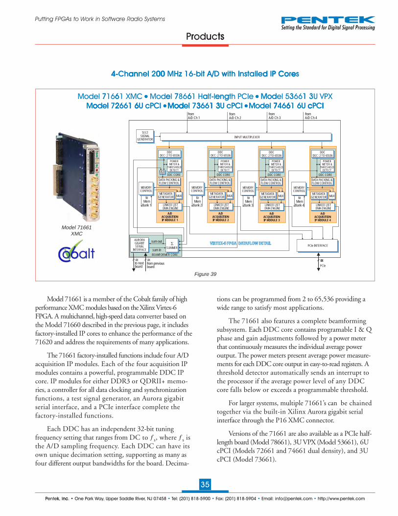
PP k nc entek, Inc. • One Park Way, Upper Saddle River, NJ 07458 • Tel: (201) 818-5900 • Fax: (201) 818-5904 • Email: [email protected] • http://www.pentek.com
35
Putting FPGAs to Work in Software Radio Systems
Figure 39
Pr tsuroducts
4-4-4-4- n / I Co ea l 00 z w l d P an l 00 z / w I l d P Co eChannel 200 MHz 16-bit A/D with Installed IP CoresChannel 200 MHz 16-bit A/D with Installed IP Cores
7 6 Model 71661 XMC ●●●●● 7 6 a - g e en Model 78661 Half-length PCIe ●●●●● Mod 3 1 3 Model 53661 3U VPXl o 2 1 6 o l 2 1 6 Model 72661 6U cPCI Model 72661 6U cPCI ● ● ● ● ● o 3 1 3 M d Mod 3 1 3 Model 73661 3U cPCI Model 73661 3U cPCI ● ● ● ● ● 7 6 c I 7 6 c IModel 74661 6U cPCIModel 74661 6U cPCI
Model 71661XMC
BEAMFORMER CORE
PCIe INTERFACE
fromA/D Ch 1
fromA/D Ch 2
fromA/D Ch 3
fromA/D Ch 4
PCIe
8Xfrom previousboard
to nextboard
sum out
sum in
VIRTEX-6 FPGA DATAFLOW DETAIL
A/DACQUISITIONIP MODULE 1
A/DACQUISITIONIP MODULE 2
A/DACQUISITIONIP MODULE 3
A/DACQUISITIONIP MODULE 4
LINKED LISTDMA ENGINE
LINKED LISTDMA ENGINE
LINKED LISTDMA ENGINE
LINKED LISTDMA ENGINE
METADATAGENERATOR
METADATAGENERATOR
METADATAGENERATOR
METADATAGENERATORto
MemBank 1
MEMORYCONTROL
toMem
Bank 2
MEMORYCONTROL
toMem
Bank 3
toMem
Bank 4
MEMORYCONTROL
MEMORYCONTROL
MUX MUX MUX MUX
DATA PACKING &FLOW CONTROL
DATA PACKING &FLOW CONTROL
DATA PACKING &FLOW CONTROL
DATA PACKING &FLOW CONTROL
AURORAGIGABITSERIAL
INTERFACE
INPUT MULTIPLEXER
�
SUMMER
DDCDEC: 2 TO 65536
DDCDEC: 2 TO 65536
DDCDEC: 2 TO 65536
DDCDEC: 2 TO 65536
POWERMETER &
THRESHOLDDETECT
POWERMETER &
THRESHOLDDETECT
POWERMETER &
THRESHOLDDETECT
POWERMETER &
THRESHOLDDETECT
MUXDDC CORE DDC CORE DDC CORE DDC CORE
TESTSIGNAL
GENERATOR
DATA PACKING &FLOW CONTROL
DATA PACKING &FLOW CONTROL
8X4X 4X
Model 71661 is a member of the Cobalt family of highperformance XMC modules based on the Xilinx Virtex-6FPGA. A multichannel, high-speed data converter based onthe Model 71660 described in the previous page, it includesfactory-installed IP cores to enhance the performance of the71620 and address the requirements of many applications.
The 71661 factory-installed functions include four A/Dacquisition IP modules. Each of the four acquisition IPmodules contains a powerful, programmable DDC IPcore. IP modules for either DDR3 or QDRII+ memo-ries, a controller for all data clocking and synchronizationfunctions, a test signal generator, an Aurora gigabitserial interface, and a PCIe interface complete thefactory-installed functions.
Each DDC has an independent 32-bit tuningfrequency setting that ranges from DC to ƒs, where ƒs isthe A/D sampling frequency. Each DDC can have itsown unique decimation setting, supporting as many asfour different output bandwidths for the board. Decima-
tions can be programmed from 2 to 65,536 providing awide range to satisfy most applications.
The 71661 also features a complete beamformingsubsystem. Each DDC core contains programable I & Qphase and gain adjustments followed by a power meterthat continuously measures the individual average poweroutput. The power meters present average power measure-ments for each DDC core output in easy-to-read registers. Athreshold detector automatically sends an interrupt tothe processor if the average power level of any DDCcore falls below or exceeds a programmable threshold.
For larger systems, multiple 71661’s can be chainedtogether via the built-in Xilinx Aurora gigabit serialinterface through the P16 XMC connector.
Versions of the 71661 are also available as a PCIe half-length board (Model 78661), 3U VPX (Model 53661), 6UcPCI (Models 72661 and 74661 dual density), and 3UcPCI (Model 73661).
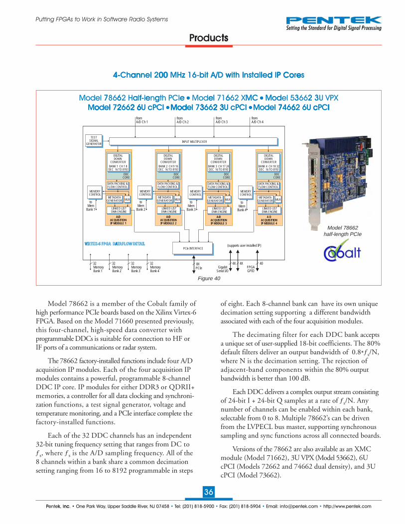
PP k nc entek, Inc. • One Park Way, Upper Saddle River, NJ 07458 • Tel: (201) 818-5900 • Fax: (201) 818-5904 • Email: [email protected] • http://www.pentek.com
36
Putting FPGAs to Work in Software Radio Systems
Figure 40
PPr u tsroductsr tsuroducts
4-4-4-4- n / I Co ea l 00 z w l d P an l 00 z / w I l d P Co eChannel 200 MHz 16-bit A/D with Installed IP CoresChannel 200 MHz 16-bit A/D with Installed IP Cores
a f g e 7 6 - e Model 78662 Half-length PCIe ●●●●● el 6 C M Model 71662 XMC ●●●●● Mod 3 2 3 Model 53662 3U VPXl o 2 2 6 o l 2 2 6 Model 72662 6U cPCI Model 72662 6U cPCI ● ● ● ● ● o 3 2 3 M d Mod 3 2 3 Model 73662 3U cPCI Model 73662 3U cPCI ● ● ● ● ● 7 6 c I 7 6 c IModel 74662 6U cPCIModel 74662 6U cPCI
Model 78662 is a member of the Cobalt family ofhigh performance PCIe boards based on the Xilinx Virtex-6FPGA. Based on the Model 71660 presented previously,this four-channel, high-speed data converter withprogrammable DDCs is suitable for connection to HF orIF ports of a communications or radar system.
The 78662 factory-installed functions include four A/Dacquisition IP modules. Each of the four acquisition IPmodules contains a powerful, programmable 8-channelDDC IP core. IP modules for either DDR3 or QDRII+memories, a controller for all data clocking and synchroni-zation functions, a test signal generator, voltage andtemperature monitoring, and a PCIe interface complete thefactory-installed functions.
Each of the 32 DDC channels has an independent32-bit tuning frequency setting that ranges from DC toƒs, where ƒs is the A/D sampling frequency. All of the8 channels within a bank share a common decimationsetting ranging from 16 to 8192 programmable in steps
of eight. Each 8-channel bank can have its own uniquedecimation setting supporting a different bandwidthassociated with each of the four acquisition modules.
The decimating filter for each DDC bank acceptsa unique set of user-supplied 18-bit coefficients. The 80%default filters deliver an output bandwidth of 0.8*ƒs/N,where N is the decimation setting. The rejection ofadjacent-band components within the 80% outputbandwidth is better than 100 dB.
Each DDC delivers a complex output stream consistingof 24-bit I + 24-bit Q samples at a rate of ƒs/N. Anynumber of channels can be enabled within each bank,selectable from 0 to 8. Multiple 78662’s can be drivenfrom the LVPECL bus master, supporting synchronoussampling and sync functions across all connected boards.
Versions of the 78662 are also available as an XMCmodule (Model 71662), 3U VPX (Model 53662), 6UcPCI (Models 72662 and 74662 dual density), and 3UcPCI (Model 73662).
Model 78662half-length PCIe
fromA/D Ch 1
fromA/D Ch 2
fromA/D Ch 3
fromA/D Ch 4
V AVIRTEX-6 FPGA DATAFLOW DETAIL
A/DACQUISITIONIP MODULE 1
A/DACQUISITIONIP MODULE 2
A/DACQUISITIONIP MODULE 3
A DACQUISITIONIP MODULE 4
LINKED LISTDMA ENGINE
LINKED LISTDMA ENGINE
METADATAGENERATOR
METADATAGENERATOR
METADATAGENERATOR
METADATAGENERATORto
MemBank 1
MEMORYCONTROL
toMem
Bank 2
MEMORYCONTROL
toMem
Bank 3
toMem
Bank 4
MEMORYCONTROL
MEMORYCONTROL
MUX MUX MUX MUX
DATA PACKING &FLOW CONTROL
DATA PACKING &FLOW CONTROL
DATA PACKING &FLOW CONTROL
DATA PACKING &FLOW CONTROL
INPUT MULTIPLEXER
TESTSIGNAL
GENERATOR
DATA PACKING &FLOW CONTROL
DATA PACKING &FLOW CONTROL
DDCCORE
DIGITALDOWN
CONVERTER
BANK 1 CH 1 8DEC 16 TO 8192
DDCCORE
DIGITALDOWN
CONVERTER
BANK 2 CH 9 16DEC 16 TO 8192
DDCCORE
DIGITALDOWN
CONVERTER
BANK 3 CH 17 24DEC 16 TO 8192
DDCCORE
DIGITALDOWN
CONVERTER
BANK 4 CH 18 32DEC 16 TO 8192
MemoryBank 4
PCIe INTERFACE
PCIe8X
LINKED LISTDMA ENGINE
LINKED LISTDMA ENGINE
GigabitSerial I/O
FPGAGPIO
(supports user installed IP)
4X 4X 4032MemoryBank 3
32MemoryBank 2
32MemoryBank 1
32

PP k nc entek, Inc. • One Park Way, Upper Saddle River, NJ 07458 • Tel: (201) 818-5900 • Fax: (201) 818-5904 • Email: [email protected] • http://www.pentek.com
37
Putting FPGAs to Work in Software Radio Systems
Figure 41
4-4- 25 H / nne w D C, Vinne 25 H / w D C, ViChannel 1.25 GHz D/A with DUC, VirChannel 1.25 GHz D/A with DUC, Vir x F G x F Gtex-6 FPGAtex-6 FPGA
7 7 Model 71670 XMC ●●●●● 7 7 a - g e en Model 78670 Half-length PCIe ●●●●● Mod 3 0 3 Model 53670 3U VPXl o 2 0 6 o l 2 0 6 Model 72670 6U cPCI Model 72670 6U cPCI ● ● ● ● ● o 3 0 3 M d Mod 3 0 3 Model 73670 3U cPCI Model 73670 3U cPCI ● ● ● ● ● 7 7 c I 7 7 c IModel 74670 6U cPCIModel 74670 6U cPCI
TIMING BUSGENERATOR
Clock / Sync /Gate / PPS
VCXOVIRTEX-6 FPGA
LX130T, LX240T, LX365T, SX315T or SX475T
16
Sample Clk /Reference Clk In
16
ConfigFLASH64 MB
16
DDR3SDRAM512 MB
DDR3SDRAM512 MB
1616
DDR3SDRAM512 MB
DDR3SDRAM512 MB
Memory Banks 1 & 2 Memory Banks 3 & 4
Clock/SyncBus A
40
GigabitSerial I/O
(option 105)
4X
GTX
4X
GTX LVDSGTX
FPGAGPIO
(option 104)
x8 PCIe
8X
P14PMC
P16XMC
P15XMC
RFXFORMR
16-BIT D/A1.25 GHz
DIGITALUPCONVERTER
RF Out
RFXFORMR
RFXFORMR
1.25 GHz16-BIT D/A
DIGITALUPCONVERTER
RF Out
RFXFORMR
RFXFORMR
16-BIT D/A1.25 GHz
DIGITALUPCONVERTER
RF Out
RFXFORMR
RFXFORMR
1.25 GHz16-BIT D/A
DIGITALUPCONVERTER
RF Out
RFXFORMR
16 16
Gate InSync In
�Sync Bus A
Gate InSync In
�Sync Bus B
Trigger In
Clock/SyncBus B
Model 71670XMC
Each member of the Cobalt family is delivered withfactory-installed applications ideally matched to the board’sanalog interfaces. The 71670 factory-installed functionsinclude four D/A waveform playback IP modules, to supportwaveform generation through the D/A converters. IP modulesfor DDR3 SDRAM memories, a controller for all dataclocking and synchronization functions, a test signal generator,and a PCIe interface complete the factory-installed functionsand enable the 71670 to operate as a complete turnkeysolution, without the need to develop any FPGA IP.
The Model 71670 factory-installed functionsinclude a sophisticated D/A Waveform Playback IPmodule. Four linked list controllers support waveformgeneration to the four D/As from tables stored in eitheron-board memory or off-board host memory.
Versions of the 71670 are also available as a PCIe half-length board (Model 78670), 3U VPX (Model 53670), 6UcPCI (Models 72679 and 74670 dual density), and 3UcPCI (Model 73670).
PPr u tsroductsr tsuroducts
Model 71670 is a member of the Cobalt family ofhigh performance XMC modules based on the XilinxVirtex-6 FPGA. This 4-channel, high-speed dataconverter is suitable for connection to transmit HF or IFports of a communications or radar system. Its built-indata playback features offer an ideal turnkey solutionfor demanding transmit applications. It includes fourD/As, four digital upconverters and four banks ofmemory. In addition to supporting PCI Express Gen. 2 asa native interface, the Model 71670 includes generalpurpose and gigabit serial connectors for application-specific I/O .
The Pentek Cobalt Architecture features a Virtex-6FPGA. All of the board’s data and control paths areaccessible by the FPGA, enabling factory-installedfunctions including data multiplexing, channel selection,data packing, gating, triggering and memory control.The Cobalt Architecture organizes the FPGA as acontainer for data processing applications where eachfunction exists as an intellectual property (IP) module.
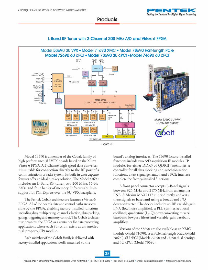
PP k nc entek, Inc. • One Park Way, Upper Saddle River, NJ 07458 • Tel: (201) 818-5900 • Fax: (201) 818-5904 • Email: [email protected] • http://www.pentek.com
38
Putting FPGAs to Work in Software Radio Systems
Figure 42
LL T T-Band RF T-Band RF Tu r w 2-u r w 2-uner with 2-uner with 2- n / iC a l 00 a VC an l 00 / a ViChannel 200 MHz A/D and VirChannel 200 MHz A/D and Vir t t tex-6 FPGAtex-6 FPGA
PX 5 9 Model 53690 3U VPX ●●●●● o 1 0 X M d Model 71690 XMC ●●●●● Mod 8 0 H h a f l g e Model 78690 Half-length PCIel o 2 0 6 o l 2 0 6 Model 72690 6U cPCI Model 72690 6U cPCI ● ● ● ● ● o 3 0 3 M d Mod 3 0 3 Model 73690 3U cPCI Model 73690 3U cPCI ● ● ● ● ● 7 9 c I 7 9 c IModel 74690 6U cPCIModel 74690 6U cPCI
PPr u tsroductsr tsuroducts
Model 53690 3U VPXCOTS and rugged
VCXOVIRTEX-6 FPGA
LX130T, LX240T, LX365T, SX315T or SX475T
16
QDRII+SRAM8 MB
TTL Gate / TrigTTL Sync / PPS
Sample ClkRef In
Gate AGate B
Sync / PPS A
Sync / PPS B
Timing Bus
Sample Clk /Reference Clk In
A/D Clock/Sync
16 16
Conf gFLASH64 MB
16
QDRII+SRAM8 MB
16
DDR3SDRAM512 MB
DDR3SDRAM512 MB
QDRII+ option 150
16
QDRII+SRAM8 MB
1616
QDRII+SRAM8 MB
16
DDR3SDRAM512 MB
DDR3SDRAM512 MB
Memory Banks 1 & 2 Memory Banks 3 & 4
DDR3 option 155
QDRII+ option 160
DDR3 option 165
Trigger 1
200 MHz16 BIT A/D
200 MHz16 BIT A/D
1616
MAX2112
I Q
XTALOSC
RefIn
RFIn
RefOut
12 BITD/A
2
I C2
GC
Control
Trigger 2
TIMINGGENERATOR
Clock / Sync /Gate / PPS
RefOption 100
40
FPGAI/O
Option -104
VPX BACKPLANE
VPX P2
GTXGTXGTXLVDS
Gigab t Serial I/O
4XGbitSerial
4XGbitSerial
4XGbitSerial
4XGbitSerial
CROSSBARSW TCH
VPX P1
4X8X 4X
x8PCIe
Model 53690 is a member of the Cobalt family ofhigh performance 3U VPX boards based on the XilinxVirtex-6 FPGA. A 2-Channel high-speed data converter,it is suitable for connection directly to the RF port of acommunications or radar system. Its built-in data capturefeatures offer an ideal turnkey solution. The Model 53690includes an L-Band RF tuner, two 200 MHz, 16-bitA/Ds and four banks of memory. It features built-insupport for PCI Express over the 3U VPX backplane.
The Pentek Cobalt architecture features a Virtex-6FPGA. All of the board’s data and control paths are acces-sible by the FPGA, enabling factory-installed functionsincluding data multiplexing, channel selection, data packing,gating, triggering and memory control. The Cobalt architec-ture organizes the FPGA as a container for data processingapplications where each function exists as an intellec-tual property (IP) module.
Each member of the Cobalt family is delivered withfactory-installed applications ideally matched to the
board’s analog interfaces. The 53690 factory-installedfunctions include two A/D acquisition IP modules. IPmodules for either DDR3 or QDRII+ memories, acontroller for all data clocking and synchronizationfunctions, a test signal generator, and a PCIe interfacecomplete the factory-installed functions.
A front panel connector accepts L-Band signalsbetween 925 MHz and 2175 MHz from an antennaLNB. A Maxim MAX2112 tuner directly convertsthese signals to baseband using a broadband I/Qdownconverter. The device includes an RF variable-gainLNA (low-noise amplifier), a PLL synthesized localoscillator, quadrature (I + Q) downconverting mixers,baseband lowpass filters and variable-gain basebandamplifiers.
Versions of the 53690 are also available as an XMCmodule (Model 71690), as a PCIe half-length board (Model78690), 6U cPCI (Models 72690 and 74690 dual density),and 3U cPCI (Model 73690).

PP k nc entek, Inc. • One Park Way, Upper Saddle River, NJ 07458 • Tel: (201) 818-5900 • Fax: (201) 818-5904 • Email: [email protected] • http://www.pentek.com
39
Putting FPGAs to Work in Software Radio Systems
4-4-4-4- nn 6-b D ra l 00 z, 1 A i h ann l 00 z, 16-b A D i h rChannel 200 MHz, 16-bit A/D with VirChannel 200 MHz, 16-bit A/D with Vir e 7 Pe 7 Ptex-7 FPGAtex-7 FPGA
7 6 Model 71760 XMC ●●●●● 7 6 a - g e en Model 78760 Half-length PCIe ●●●●● Mod 3 0 3 Model 53760 3U VPXo l 2 0 6 Model 72760 6U cPCI l o 2 0 6 Model 72760 6U cPCI ● ● ● ● ● Mod 3 0 3 Model 73760 3U cPCI o 3 0 3 M d Model 73760 3U cPCI ● ● ● ● ● 7 6 c IModel 74760 6U cPCI 7 6 c IModel 74760 6U cPCI
Figure 43
PPr u tsroductsr tsuroducts
Model 71760XMC
TIMING BUSGENERATOR
Clock / Sync /Gate / PPS
VCXO
200 MHz16-BIT A/D
RF In
RFXFORMR
RF In
RFXFORMR
VIRTEX-7 FPGA
VX330T, VX485T or VX690T
32
TTL Gate / TrigTTL Sync / PPS
Sample ClkReset
Gate AGate B
Sync / PPS A
Sync / PPS B
Timing Bus
200 MHz16-BIT A/D
Sample Clk /Reference Clk In
A/D Clock/Sync Bus
1616
16
ConfigFLASH128 MB
32
DDR3SDRAM
1 GB
DDR3SDRAM
1 GB
3232
DDR3SDRAM
1 GB
DDR3SDRAM
1 GB
RF In
RFXFORMR
200 MHz16-BIT A/D
16
RF In
RFXFORMR
200 MHz16-BIT A/D
16
Gate / Trigger /Sync / PPS
48
GigabitSerial I/O
(option 105)
4X
GTX
4X8X
GTX LVDSGTX
FPGAGPIO
(option 104)
P14PMC
P16XMC
P15XMC
PCIeGen3 x8
Model 71760 is a member of the OnyxTM family ofhigh performance XMC modules based on the XilinxVirtex-7 FPGA. A multichannel, high-speed data converter,it is suitable for connection to HF or IF ports of acommunications or radar system. Its built-in data capturefeatures offer an ideal turnkey solution as well as aplatform for developing and deploying custom FPGAprocessing IP. It includes four A/Ds and four banks ofmemory. In addition to supporting PCI Express Gen. 3 as anative interface, the Model 71760 includes general purposeand gigabit serial connectors for application-specific I/O.
Based on the proven design of the Pentek Cobalt family,Onyx raises the processing performance with the new flagshipfamily of Virtex-7 FPGAs from Xilinx. As the central feature ofthe board architecture, the FPGA has access to all data andcontrol paths, enabling factory-installed functions including datamultiplexing, channel selection, data packing, gating, triggeringand memory control. The Onyx Architecture organizes theFPGA as a container for data processing applications where eachfunction exists as an intellectual property (IP) module.
Each member of the Onyx family is delivered with factory-installed applications ideally matched to the board’s analoginterfaces. The 71760 factory-installed functions include fourA/D acquisition IP modules for simplifying data capture anddata tranfer. IP modules for DDR3 SDRAM memories, acontroller for all data clocking and synchronization functions, atest signal generator, and a PCIe interface complete the factory-installed functions and enable the 71760 to operate as a completeturnkey solution without the need to develop any FPGA IP.
The 71760 architecture supports four independentDDR3 SDRAM memory banks. Each bank is 1 GB deepand is an integral part of the module’s DMA capabili-ties, providing FIFO memory space for creating DMApackets. Built-in memory functions include multichannelA/D data capture, tagging and streaming.
Versions of the 71760 are also available as a PCIe half-length board (Model 78760), 3U VPX (Model 53760), 6UcPCI (Models 72760 and 74760 dual density), and 3UcPCI (Model 73760).

PP k nc entek, Inc. • One Park Way, Upper Saddle River, NJ 07458 • Tel: (201) 818-5900 • Fax: (201) 818-5904 • Email: [email protected] • http://www.pentek.com
40
Putting FPGAs to Work in Software Radio Systems
PP odu troductsodu troducts
M H / MH / 215 MHz, 12-bit A/D with W215 MHz, 12-bit A/D with W a - VXSd b D d ba D - VXSideband DDCs - VME/VXSideband DDCs - VME/VXS
The Model 6821 is a 6U single slot board with theAD9430 12-bit, 215 MHz A/D converter.
Capable of digitizing input signal bandwidths up to100 MHz, it is ideal for wideband applications includ-ing radar and spread spectrum communication systems.
The sampling clock can be supplied either from afront panel input or from an internal crystal oscillator.Data from the A/D converter flows into two XilinxVirtex-II Pro FPGAs where optional signal processingfunctions can be performed. The size of the FPGAs canrange from the XC2VP20 to the XC2VP50.
Because the sampling rate is well beyond conven-tional ASIC digital downconverters, none are includedon the board.
Instead, the Pentek GateFlow IP Core 422 UltraWideband Digital Downconverter can be factory-
installed in one or both of the FPGAs to perform thisfunction.
Two 128 MB SDRAMs, one for each FPGA,support large memory applications such as swingingbuffers, digital filters, DSP algorithms, and digital delaylines for tracking receivers.
Either two or four FPDP-II ports connect the FPGAsto external digital destinations such as processor boards,memory boards or storage devices.
A VMEbus interface supports configuration of theFPGAs over the backplane and also provides data andcontrol paths for runtime applications. A VXS interfaceis optionally available.
This Model is available in commercial as well asconduction-cooled versions.
Figure 44
e d Model 6821-422
128kFIFO
FPDP-IIOut CSlot 2
FPDP-IIOut BSlot 1
32 32

PP k nc entek, Inc. • One Park Way, Upper Saddle River, NJ 07458 • Tel: (201) 818-5900 • Fax: (201) 818-5904 • Email: [email protected] • http://www.pentek.com
41
Putting FPGAs to Work in Software Radio Systems
PP odu troductsodu troducts
M / H i w W MH i / w WDual 215 MHz, 12-bit A/D with WDual 215 MHz, 12-bit A/D with W a Vd b D d ba D Videband DDCs - VME/VXSideband DDCs - VME/VXS
The Model 6822 is a 6U single slot VME boardwith two AD9430 12-bit 215 MHz A/D converters.
Capable of digitizing input signal bandwidths up to100 MHz, it is ideal for wideband applications includ-ing radar and spread spectrum communication systems.
The sampling clock can be supplied either from afront panel input or from an internal crystal oscillator.Data from each A/D converter flows into a XilinxVirtex-II Pro FPGA where optional signal processingfunctions can be performed. The size of the FPGAs canrange from the XC2VP20 to the XC2VP50.
Because the sampling rate is well beyond conven-tional ASIC digital downconverters, none are includedon the board.
Instead, the Pentek GateFlow IP Core 422 UltraWideband Digital Downconverter can be factory-
installed in one or both of the FPGAs to perform thisfunction.
Two 128 MB SDRAMs, one for each FPGA,support large memory applications such as swingingbuffers, digital filters, DSP algorithms, and digital delaylines for tracking receivers.
Either two or four FPDP-II ports connect the FPGAsto external digital destinations such as processor boards,memory boards or storage devices.
A VMEbus interface supports configuration of theFPGAs over the backplane and also provides data andcontrol paths for runtime applications. A VXS interfaceis optionally available.
This Model is available in commercial as well asconduction-cooled versions.
e d Model 6822-422
Figure 45

PP k nc entek, Inc. • One Park Way, Upper Saddle River, NJ 07458 • Tel: (201) 818-5900 • Fax: (201) 818-5904 • Email: [email protected] • http://www.pentek.com
42
Putting FPGAs to Work in Software Radio Systems
PP odu troductsodu troducts
u 0-b G z, 1 A i h u G z, 10-b A i h Dual 2 GHz, 10-bit A/D with VDual 2 GHz, 10-bit A/D with V rrerery e D i p D VME/y i pe DD VME/y High-Speed DDCs - VME/VXSy High-Speed DDCs - VME/VXS
The Model 6826 is a 6U single slot VME boardwith two Atmel AT84AS008 10-bit 2 GHz A/Dconverters.
Capable of digitizing input signals at sampling ratesup to 2 GHz, it is ideal for extremely widebandapplications including radar and spread spectrumcommunication systems. The sampling clock is anexternally supplied sinusoidal clock at a frequency from200 MHz to 2 GHz.
Data from each of the two A/D converters flowsinto an innovative dual-stage demultiplexer that packsgroups of eight data samples into 80-bit words fordelivery to the Xilinx Virtex-II Pro XC2VP70 FPGAat one eighth the sampling frequency. This advancedcircuit features the Atmel AT84CS001 demultiplexerwhich represents a significant improvement over previoustechnology.
Because the sampling rate is well beyond conven-tional digital downconverters, none are included on theboard. A very high-speed digital downconverter IP core
d l 6826Model 6826d 6826l Model 6826
Figure 46
for the Model 6826 can be developed for a customer whois interested in one.
The customer will be able to incorporate this coreinto the Model 6826 by ordering it as a factory-installedoption.
Two 512 MB or 1 GB SDRAMs, support largememory applications such as swinging buffers, digitalfilters, DSP algorithms, and digital delay lines fortracking receivers.
Either two or four FPDP-II ports connect the FPGAto external digital destinations such as processor boards,memory boards or storage devices.
A VMEbus interface supports configuration of theFPGA over the backplane and also provides data andcontrol paths for runtime applications. A VXS interfaceis optionally available.
This Model is also available in a single-channelversion and in commercial as well as conduction-cooledversions.
4:1
DEMUX
AT84CS001
40 2:1
DEMUX
V4 FPGA
10
40 2:1
DEMUX
V4 FPGA
10 4:1
DEMUX
AT84CS001
16 MB
FLASH
16
VMEbus
VME SLAVE
INTERFACE
Model 6826
128k
FIFO
FPDP-II
400 MB/sec
32 32
128k
FIFO
32
4:1
DEMUX
AT84CS001
40 2:1
DEMUX
V4 FPGA
10
40 2:1
DEMUX
V4 FPGA
10 4:1
DEMUX
AT84CS001

PP k nc entek, Inc. • One Park Way, Upper Saddle River, NJ 07458 • Tel: (201) 818-5900 • Fax: (201) 818-5904 • Email: [email protected] • http://www.pentek.com
43
Putting FPGAs to Work in Software Radio Systems
P odu troducts
Figure 47
6 0 - Ve e 6 0 - VModel 6890 - VMEModel 6890 - VME
l , y c a i k S n G i d2.2 GHz Clock, Sync and Gate Distribution Board
BUFFER1:2
BUFFER1:2
BUFFER1:2
PROGDELAY
PROGDELAY
MUX2:1
MUX2:1
FrontPanelSync
Output
FrontPanelClockOutput
FrontPanelGate
Output
Ch 1
Ch 1
Ch 1
Ch 2
Ch 2
Ch 2
Ch 3
Ch 3
Ch 3
Ch 4
Ch 4
Ch 4
Ch 5
Ch 5
Ch 5
Ch 6
Ch 6
Ch 6
Ch 7
Ch 7
Ch 7
Ch 8
Ch 8
Ch 8
LVPECLBUFFER
1 8
LVPECLBUFFER
1 8
POWERSPL TTER
1:8
POWERSPLITTER
1:2
TTL / PECLSELECTOR
TTL / PECLSELECTOR
TTL / PECLSELECTOR
TTL / PECLSELECTOR
GATECONTROL
SYNCCONTROL
FrontPanelClockInput
FrontPanelGateInput
FrontPanelSyncInput
FrontPanelGate
Enable
FrontPanelSync
Enable REG
REG
Model 6890VME
Model 6890 Clock, Sync and Gate DistributionBoard synchronizes multiple Pentek I/O boards within asystem. It enables synchronous sampling and timingfor a wide range of multichannel high-speed dataacquisition, DSP and software radio applications. Upto eight boards can be synchronized using the 6890,each receiving a common clock of up to 2.2 GHz alongwith timing signals that can be used for synchronizing,triggering and gating functions.
Clock signals are applied from an external sourcesuch as a high performance sine wave generator. Gateand sync signals can come from an external source, orfrom one supported board set to act as the master.
The 6890 accepts clock input at +10 dBm to +14 dBmwith a frequency range from 800 MHz to 2.2 GHz anduses a 1:2 power splitter to distribute the clock. The firstoutput of this power splitter sends the clock signal to a1:8 splitter for distribution to up to eight boards usingSMA connectors. The second output of the 1:2 power
splitter feeds a 1:2 buffer which distributes the clocksignal to both the gate and synchronization circuits.
The 6890 features separate inputs for gate/triggerand sync signals with user-selectable polarity. Each ofthese inputs can be TTL or LVPECL. Separate GateEnable and Sync Enable inputs allow the user to enableor disable these circuits using an external signal.
A programmable delay allows the user to maketiming adjustments on the gate and sync signals beforethey are sent to an LVPECL buffer. A bank of eightMMCX connectors at the output of each buffer deliverssignals to up to eight boards.
A 2:1 multiplexer in each circuit allows the gate/trigger and sync signals to be registered with the inputclock signal before output, if desired.
Sets of input and output cables for two to eightboards are available from Pentek.

PP k nc entek, Inc. • One Park Way, Upper Saddle River, NJ 07458 • Tel: (201) 818-5900 • Fax: (201) 818-5904 • Email: [email protected] • http://www.pentek.com
44
Putting FPGAs to Work in Software Radio Systems
P odu troducts
S s y r t i re S nc ni t o aSystem Synchronizer and Distribution Board
6 1 - Ve e 6 1 - VModel 6891 - VMEModel 6891 - VME
BUFFER1 2
BUFFER1 2
PROGDELAY
PROGDELAY
MUX2:1
MUX2:1
Ch 1
Ch 1
Ch 1
Ch 2
Ch 2
Ch 2
Ch 3
Ch 3
Ch 3
Ch 4
Ch 4
Ch 4
Ch 5
Ch 5
Ch 5
Ch 6
Ch 6
Ch 6
Ch 7
Ch 7
Ch 7
Ch 8
Ch 8
Ch 8
SYNCLVPECLBUFFER
1 8
GATELVPECLBUFFER
1 8
CLOCKLVPECLBUFFER
1 10
GATECONTROL
F ont PanelClock Input
F ont PanelGateInput
Front PanelSync Input
F ont PanelGate Enable
Front PanelSync Enable REG
REG
Gate
SyncClockSync Bus
Input
MUX2 1
MUX2 1
MUX2 1
SYNCCONTROL
Gate
SyncClock Sync Bus
Output 8
Gate
SyncClock Sync Bus
Output 7
Gate
SyncClock Sync Bus
Output 6
Gate
SyncClock Sync Bus
Output 5
Gate
SyncClock Sync Bus
Output 4
Gate
SyncClock Sync Bus
Output 3
Gate
SyncClock Sync Bus
Output 2
Gate
SyncClock Sync Bus
Output 1
to Sync BusOutputs 2-8
to Sync BusOutputs 2-8
to Sync BusOutputs 2-8
Model 6891VME
Model 6891 System Synchronizer and DistributionBoard synchronizes multiple Pentek I/O modules within asystem. It enables synchronous sampling and timing for awide range of multichannel high-speed data acquisition,DSP and software radio applications.
Up to eight modules can be synchronized using the6891, each receiving a common clock up to 500 MHzalong with timing signals that can be used for synchroniz-ing, triggering and gating functions. For larger systems,up to eight 6891’s can be linked together to providesynchronization for up to 64 I/O modules producingsystems with up to 256 channels.
Model 6891 accepts three TTL input signals fromexternal sources: one for clock, one for gate or triggerand one for a synchronization signal. Two additionalinputs are provided for separate gate and sync enable signals.
Clock signals can be applied from an external sourcesuch as a high performance sine-wave generator. Gate/triggerand sync signals can come from an external system source.Alternately, a Sync Bus connector accepts LVPECL inputsfrom any compatible Pentek products to drive the clock,sync and gate/trigger signals.
The 6891 provides eight front panel Sync Bus outputconnectors, compatible with a wide range of Pentek I/Omodules. The Sync Bus is distributed through ribboncables, simplifying system design. The 6891 accepts clockinput at +10 dBm to +14 dBm with a frequency rangefrom 1 kHz to 800 MHz. This clock is used to registerall sync and gate/trigger signals as well as providing asample clock to all connected I/O modules.
A programmable delay allows the user to maketiming adjustments on the gate and sync signals beforethey are sent to an LVPECL buffer for output throughthe Sync Bus connectors.
Figure 48

PP k nc entek, Inc. • One Park Way, Upper Saddle River, NJ 07458 • Tel: (201) 818-5900 • Fax: (201) 818-5904 • Email: [email protected] • http://www.pentek.com
45
Putting FPGAs to Work in Software Radio Systems
ReferenceIn
Control
PCI INTERFACE
PCI BUS(32 Bits / 66 MHz)32
Clock Out1
Clock Out2
Clock Out3
Clock Out4
Clock Out5
Clock Out6
Clock Out7
Clock Out8
CLOCKSYNTHESIZER
AND JITTERCLEANER
A
1÷÷ 2÷ 4÷ 8÷16
QUADVCXO
A
CLOCKSYNTHESIZER
AND JITTERCLEANER
B
1÷÷ 2÷ 4÷ 8÷16
CLOCKSYNTHESIZER
AND JITTERCLEANER
C
1÷÷ 2÷ 4÷ 8÷16
CLOCKSYNTHESIZER
AND JITTERCLEANER
D
1÷÷ 2÷ 4÷ 8÷16
CROSSBAR
SWITCH
In
In
In
In
Out
Out
Out
Out
Out
QUADVCXO
B
QUADVCXO
C
QUADVCXO
D
PP odu todu troductsroducts
Figure 49
nc C et f l c e zt f nc Cl c e zeMultifrequency Clock SynthesizerMultifrequency Clock Synthesizer
Model 7190PMC
Model 7190 generates up to eight synthesized clocksignals suitable for driving A/D and D/A converters inhigh-performance real-time data acquisition and softwareradio systems. The clocks offer exceptionally low phase noiseand jitter to preserve the signal quality of the data converters.These clocks are synthesized from on-board quad VCXOsand can be phase-locked to an external reference signal.
The 7190 uses four Texas Instruments CDC7005 clocksynthesizer and jitter cleaner devices. Each CDC7005 is pairedwith a dedicated VCXO to provide the base frequency forthe clock synthesizer. Each of the four VCXOs can beindependently programmed to generate one of four frequen-cies between 50 MHz and 700 MHz.
The CDC7005 can output the selected frequencyof its associated VCXO, or generate submultiples usingdivisors of 2, 4, 8 or 16. The four CDC7005’s can outputup to five frequencies each. The 7190 can be programmed toroute any of these 20 frequencies to the module’s fiveoutput drivers.
The CDC7005 includes phase-locking circuitrythat locks the frequency of its associated VCXO to aninput reference of 5 MHz to 100 MHz.
Eight front panel SMC connectors supply synthesizedclock outputs driven from the five clock output drivers.This supports a single identical clock to all eight outputsor up to five different clocks to various outputs. Withfour independent quad VCXOs and each CDC7005capable of providing up to five different submultipleclocks, a wide range of clock configurations is possible. Insystems where more than five different clock outputs arerequired simultaneously, multiple 7190’s can be used andphase-locked with the 5 MHz to 100 MHz system reference.
Versions of the 7190 are also available as a PCIe full-length board (Models 7790 and 7790D dual density),PCIe half-length board (Model 7890), 3U VPX board(Model 5390), PCI board (Model 7690), 6U cPCI(Models 7290 and 7290D dual density), or 3U cPCI(Model 7390).
e l 1 C Model 7190 PMC ●●●●● Mod 6 7 0 I Model 7290 6U cPCI ●●●●● 9 P e U Model 7390 3U cPCI ●●●●● l 6 I o PC Model 7690 PCIMod 7 Mod 7 Model 7790 FModel 7790 F l n t PCI l n t PCI ull-length PCIe ull-length PCIe ●●●●● l 9 a - g e o e o l 9 a - e g e Model 7890 Half-length PCIe Model 7890 Half-length PCIe ●●●●● e 3 l 9 PX el 9 3 PX Model 5390 3U VPX Model 5390 3U VPX

PP k nc entek, Inc. • One Park Way, Upper Saddle River, NJ 07458 • Tel: (201) 818-5900 • Fax: (201) 818-5904 • Email: [email protected] • http://www.pentek.com
46
Putting FPGAs to Work in Software Radio Systems
ReferenceIn
Control
PCI INTERFACE
PCI BUS(32 Bits / 66 MHz)32
Clock Out1
Clock Out2
Clock Out3
Clock Out4
Clock Out5
Clock Out6
Clock Out7
Clock Out8
CLOCKSYNTHESIZER
AND JITTERCLEANER
A
1÷÷ 2÷ 4÷ 8÷16
PROGRAMVCXO
A
CLOCKSYNTHESIZER
AND JITTERCLEANER
B
1÷÷ 2÷ 4÷ 8÷16
CLOCKSYNTHESIZER
AND JITTERCLEANER
C
1÷÷ 2÷ 4÷ 8÷16
CLOCKSYNTHESIZER
AND JITTERCLEANER
D
1÷÷ 2÷ 4÷ 8÷16
CROSSBAR
SWITCH
In
In
In
In
Out
Out
Out
Out
Out
PROGRAMVCXO
B
PROGRAMVCXO
C
PROGRAMVCXO
D
PP odu todu troductsroducts
Figure 50
PP a ul i r q zo e nc Cl c heo a e ul i r q nc Cl c he zrogrammable Multifrequency Clock Synthesizerrogrammable Multifrequency Clock Synthesizer
e l 1 C Model 7191 PMC ●●●●● Mod 6 7 1 I Model 7291 6U cPCI ●●●●● 9 P e U Model 7391 3U cPCI ●●●●● l 6 I o PC Model 7691 PCIMod 7 Mod 7 Model 7791 FModel 7791 F l n t PCI l n t PCI ull-length PCIe ull-length PCIe ●●●●● l 9 a - g e o e o l 9 a - e g e Model 7891 Half-length PCIe Model 7891 Half-length PCIe ●●●●● e 3 l 9 PX el 9 3 PX Model 5391 3U VPX Model 5391 3U VPX
Model 7191 generates up to eight synthesized clocksignals suitable for driving A/D and D/A converters inhigh-performance real-time data acquisition and softwareradio systems. The clocks offer exceptionally low phase noiseand jitter to preserve the signal quality of the data converters.These clocks are synthesized from programmable VCXOsand can be phase-locked to an external reference signal.
The 7191 uses four Texas Instruments CDC7005 clocksynthesizer and jitter cleaner devices. Each CDC7005 is pairedwith a dedicated VCXO to provide the base frequency forthe clock synthesizer. Each of the four VCXOs can beindependently programmed to a desired frequency between50 MHz and 700 MHz with 32-bit tuning resolution.
The CDC7005 can output the programmed frequencyof its associated VCXO, or generate submultiples usingdivisors of 2, 4, 8 or 16. The four CDC7005’s can outputup to five frequencies each. The 7191 can be programmed toroute any of these 20 frequencies to the module’s fiveoutput drivers.
The CDC7005 includes phase-locking circuitrythat locks the frequency of its associated VCXO to aninput reference of 5 MHz to 100 MHz.
Eight front panel SMC connectors supply synthesizedclock outputs driven from the five clock output drivers.This supports a single identical clock to all eight outputsor up to five different clocks to various outputs. Withfour programmable VCXOs and each CDC7005capable of providing up to five different submultipleclocks, a wide range of clock configurations is possible. Insystems where more than five different clock outputs arerequired simultaneously, multiple 7191’s can be used andphase-locked with the 5 MHz to 100 MHz system reference.
Versions of the 7191 are also available as a PCIe full-length board (Models 7791 and 7791D dual density),PCIe half-length board (Model 7891), 3U VPX board(Model 5391), PCI board (Model 7691), 6U cPCI(Models 7291 and 7291D dual density), or 3U cPCI(Model 7391).
Model 7191PMC

PP k nc entek, Inc. • One Park Way, Upper Saddle River, NJ 07458 • Tel: (201) 818-5900 • Fax: (201) 818-5904 • Email: [email protected] • http://www.pentek.com
47
Putting FPGAs to Work in Software Radio Systems
Figure 51
M d /XM 7 2 PMC Model 7192 PMC/XMC ●●●●● M d l t PC 7 2 H h Model 7892 Half-length PCIe ●●●●● 5 3 3 Model 5393 3U VPX 7 2 e 9 e 7 92 Model 7292 6U cPCI Model 7292 6U cPCI ●●●●● o 3 U cPC M d Mod 3 U cPC Model 7392 3U cPCI Model 7392 3U cPCI ● ● ● ● ● c CIod 4 U Pod 4 U cPCIModel 7492 6U cPCIModel 7492 6U cPCI
H g d y r n s r u re c ni a D b i n aH g e d y c ni r an D s r bu i n arHigh-Speed Synchronizer and Distribution BoardHigh-Speed Synchronizer and Distribution Board
Model 7192PMC/XMC
PLL&
DIVIDER
Gate / Trigger Out
Sample Clk /Reference
Clk InMUX
ClkIn
RefIn
N
PROGRAMMABLEVCXO
Clock /Calibration Out
N
BUFFER&
PROGRAMDELAYS
Clk/RefIn
Sync OutReference Clk Out
TWSI Control InReference Clk In *
Gate / Trigger OutSync OutReference Clk Out
MUX
Trig/GateIn
SyncIn
TWSICONTROL
Gate / Trigger OutSync OutReference Clk Out
Gate / Trigger OutSync OutReference Clk Out
Gate / Trigger In
Sync In
�Sync 3
�Sync 2
�Sync 1
�Sync 4
* For 71640 A/D calibration
The Model 7192 High-Speed Synchronizer andDistribution Board synchronizes multiple Pentek Cobaltor Onyx modules within a system. It enables synchronoussampling and timing for a wide range of multichannelhigh-speed data acquisition, DSP, and software radioapplications. Up to four modules can be synchronizedusing the 7192, with each receiving a common clockalong with timing signals that can be used for synchro-nizing, triggering and gating functions.
Model 7192 provides three front panel MMCXconnectors to accept input signals from external sources:one for clock, one for gate or trigger and one for a synchro-nization signal. Clock signals can be applied from anexternal source such as a high performance sine-wavegenerator. Gate/trigger and sync signals can come froman external system source. In addition to the MMCXconnector, a reference clock can be accepted through thefirst front panel µSync output connector, allowing asingle Cobalt or Onyx board to generate the clock forall subsequent boards in the system.
The 7192 provides four front panel µSync outputconnectors, compatible with a range of high-speedPentek Cobalt and Onyx modules. The µSync signalsinclude a reference clock, gate/trigger and sync signals and aredistributed through matched cables, simplifying systemdesign. The 7192 features a calibration output specifi-cally designed to work with the 71640 or 717403.6 GHz A/D module and provide a signal reference forphase adjustment across multiple D/As.
The 7192 supports all high-speed models in the Cobaltfamily including the 71630 1 GHz A/D and D/A XMC,the 71640 3.6 GHz A/D XMC and the 71670 Four-channel 1.25 GHz, 16-bit D/A XMC. The 7192 will alsosupport high-speed models in the Onyx family as theybecome available.
Versions of the 7192 are also available as a PCIe half-length board (Model 7892), 3U VPX (Model 5392), 6UcPCI (Models 7292 and 7492 dual density), and 3UcPCI (Model 7392).
PPr tsur u tsroductsroducts

PP k nc entek, Inc. • One Park Way, Upper Saddle River, NJ 07458 • Tel: (201) 818-5900 • Fax: (201) 818-5904 • Email: [email protected] • http://www.pentek.com
48
Putting FPGAs to Work in Software Radio Systems
Figure 52
7 3 - H h e f l eModel 7893 - Half-length PCIe
t hr i dy e i By t hr e i i B dSystem Synchronizer and Distribution BoardSystem Synchronizer and Distribution Board
PPr tsur u tsroductsroducts
PLL&
DIVIDER
CLKIN
PROGRAMVCXO
Clock Out 1N
BUFFER&
PROGRAMDELAYS
TTLSync / PPS B In
Timing Bus Out 2through
Timing Bus Out 7
USBINTERFACE
USB
Sample Clk A
Sample Clk BGate / Trig AGate / Trig B
Sync / PPS A
Sync / PPS B
Timing Bus In
Sample Clk ASample Clk BGate / Trig AGate / Trig BSync / PPS A
Sync / PPS B
Timing Bus Out 1
Sample Clk ASample Clk BGate / Trig AGate / Trig BSync / PPS A
Sync / PPS B
Timing Bus Out 8
MUX
TTLSync / PPS A In
MUX
MUX
MUX
TTLGate / Trig In
MUX
Sample Clk /Reference Clk In
Clock Out 2
Clock Out 3
Clock Out 4
N
N
N
N
Gate / Trig A
Gate / Trig B
Sync / PPS A
Sync / PPS B
MUX
USB Sync / PPS
USB Gate / Trig
REFCLKIN
CONTROLVOLTAGE
Sample Clk A
Sample Clk B
Sample Clk A
Sample Clk B
Control
USB Gate / Trig
USB Sync / PPS
Model 7893 System Synchronizer and DistributionBoard synchronizes multiple Pentek Cobalt and Onyxboards within a system. It enables synchronous sampling,playback and timing for a wide range of multichannelhigh-speed data acquisition, DSP and software radioapplications.
Up to eight boards can be synchronized using the7893, each receiving a common clock up to 800 MHzalong with timing signals that can be used for synchroniz-ing, triggering and gating functions. For larger systems,up to eight 7893s can be linked together to provide synchro-nization for up to 64 Cobalt or Onyx boards.
The Model 7893 provides four front panel SMAconnectors to accept LVTTL input signals fromexternal sources: two for Sync/PPS and one for Gate/Trigger. In addition to the synchronization signals, a frontpanel SMA connector accepts sample clocks up to 800 MHzor, in an alternate mode, accepts a 10 MHz referenceclock to lock an on-board VCXO sample clock source.
The 7893 provides eight timing bus output connec-tors for distributing all needed timing and clock signalsto the front panels of Cobalt and Onyx boards via ribboncables. The 7893 locks the Gate/Trigger and Sync/PPSsignals to the system’s sample clock. The 7893 alsoprovides four front panel SMA connectors for distrib-uting sample clocks to other boards in the system.
The 7893 can accept a clock from either the front panelSMA connector or from the timing bus input connector. Aprogrammable on-board VCXO clock generator can belocked to a user-supplied, 10 MHz reference.
The 7893 supports a wide range of products in theCobalt family including the 78620 and 78621 three-channelA/D 200 MHz transceivers, the 78650 and 78651 two-channelA/D 500 MHz transceivers, the 78660, 78661 and 78662four-channel 200 MHz A/Ds, and the 78690 L-Band RFTuner. The 7893 also supports the Onyx 78760 four-channel 200 MHz A/D and will support all complemen-tary models in the Onyx family as they become available.

PP k nc entek, Inc. • One Park Way, Upper Saddle River, NJ 07458 • Tel: (201) 818-5900 • Fax: (201) 818-5904 • Email: [email protected] • http://www.pentek.com
49
Putting FPGAs to Work in Software Radio Systems
PP odu todu troductsroducts
Figure 53
Cl c a o / d ne o r eCl c ne a o or / d eClock and Sync Generator for I/O ModulesClock and Sync Generator for I/O Modules
ToModuleNo. 80
FromModuleMasterSource
ToModuleNo. 2
ToModuleNo. 1
OPTIONALINTERNAL
OSCILLATOR
LVDSDIFF.
RECEIVER
LVDSDIFF.
DRIVERS
LVDSDIFF.
DRIVERS
LVDSDIFF.
DRIVERS
FrontPanelOutputSMA
Connectors
LINEDRIVERS
FrontPanelInputSMA
Connectors
TimingSignals
MultiplexerSwitches
TimingSignals
TimingSignals
Ext. Clock
ClockLINERCVRS
Model 9190
l 9 o 1 Model 9190 - Ra m noackmount
Model 9190 Clock and Sync Generator synchronizesmultiple Pentek I/O modules within a system to providesynchronous sampling and timing for a wide range ofhigh-speed, multichannel data acquisition, DSP andsoftware radio applications. Up to 80 I/O modules canbe driven from the Model 9190, each receiving acommon clock and up to five different timing signalswhich can be used for synchronizing, triggering andgating functions.
Clock and timing signals can come from six frontpanel SMA user inputs or from one I/O module set to actas the timing signal master. (In this case, the master I/Omodule will not be synchronous with the slave modulesdue to delays through the 9190.) Alternately, the masterclock can come from a socketed, user-replaceable crystaloscillator within the Model 9190.
Buffered versions of the clock and five timingsignals are available as outputs on the 9190’s front panelSMA connectors.
Model 9190 is housed in a line-powered, 1.75 in.high metal chassis suitable for mounting in a standard19 in. equipment rack, either above or below the cageholding the I/O modules.
Separate cable assemblies extend from openings inthe front panel of the 9190 to the front panel clock andsync connectors of each I/O module. Mounted betweentwo standard rack-mount card cages, Model 9190 candrive a maximum of 80 clock and sync cables, 40 to thecard cage above and 40 to the card cage below. Fewercables may be installed for smaller systems.
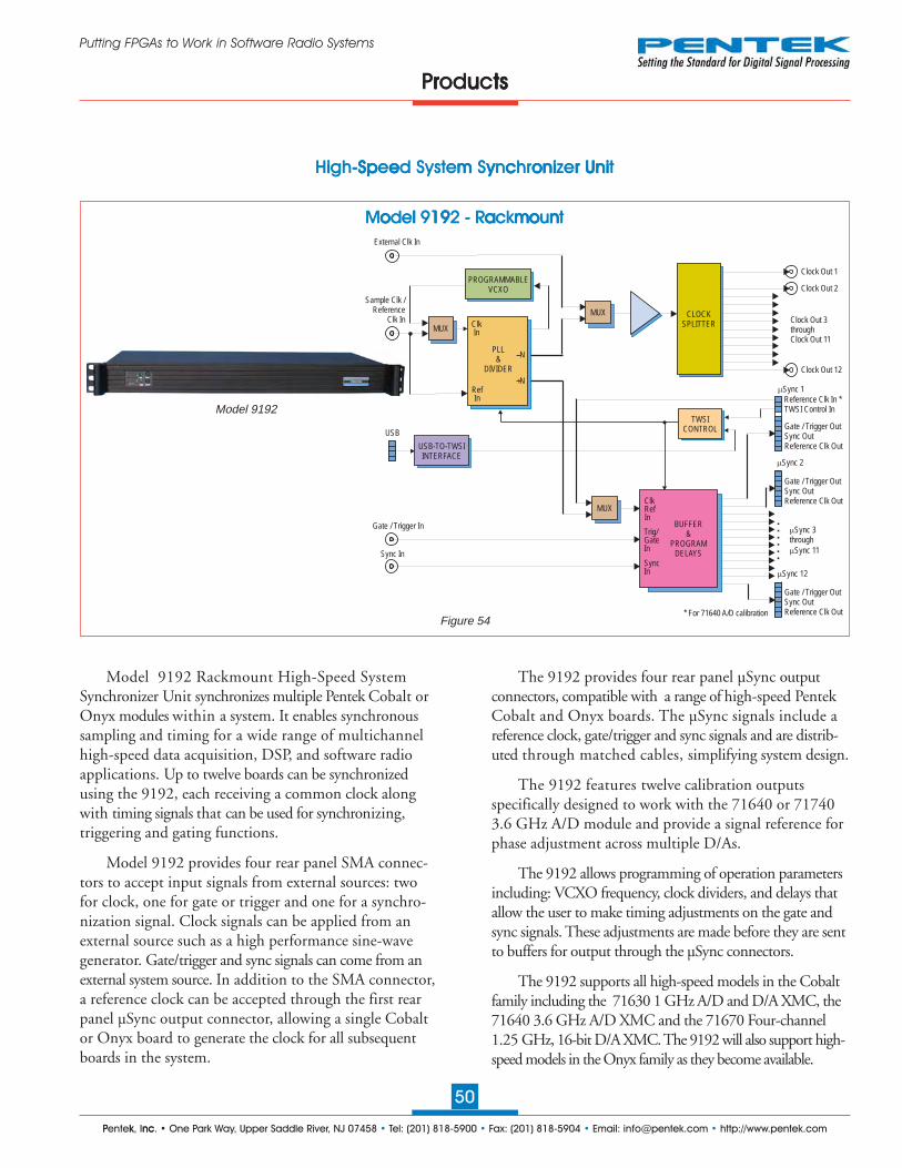
PP k nc entek, Inc. • One Park Way, Upper Saddle River, NJ 07458 • Tel: (201) 818-5900 • Fax: (201) 818-5904 • Email: [email protected] • http://www.pentek.com
50
Putting FPGAs to Work in Software Radio Systems
PPr tsur u tsroductsroducts
i p e y o r ni-S m c ni Ui -Sp e m y c oni r UniHigh-Speed System Synchronizer UnitHigh-Speed System Synchronizer Unit
o l 19 Model 9192 - Rl 9 o 1 Model 9192 - Ra mo nackmounta m noackmount
PLL&
DIVIDER
Gate / Trigger Out
Sample Clk /Reference
Clk InMUX
ClkIn
RefIn
:N
PROGRAMMABLEVCXO
Clock Out 1
N
BUFFER&
PROGRAMDELAYS
ClkRefIn
Sync OutReference Clk Out
TWSI Control InReference Clk In *
Gate / Trigger OutSync OutReference Clk Out
MUX
Trig/GateIn
SyncIn
TWSICONTROL
Gate / Trigger OutSync OutReference Clk Out
Gate / Trigger In
Sync In
�Sync 2
�Sync 1
�Sync 12
* For 71640 A/D calibration
�Sync 3through
�Sync 11
Clock Out 2
Clock Out 12
CLOCKSPLITTER
Clock Out 3throughClock Out 11
External Clk In
MUX
USB-TO-TWSIINTERFACE
USB
Model 9192
Model 9192 Rackmount High-Speed SystemSynchronizer Unit synchronizes multiple Pentek Cobalt orOnyx modules within a system. It enables synchronoussampling and timing for a wide range of multichannelhigh-speed data acquisition, DSP, and software radioapplications. Up to twelve boards can be synchronizedusing the 9192, each receiving a common clock alongwith timing signals that can be used for synchronizing,triggering and gating functions.
Model 9192 provides four rear panel SMA connec-tors to accept input signals from external sources: twofor clock, one for gate or trigger and one for a synchro-nization signal. Clock signals can be applied from anexternal source such as a high performance sine-wavegenerator. Gate/trigger and sync signals can come from anexternal system source. In addition to the SMA connector,a reference clock can be accepted through the first rearpanel µSync output connector, allowing a single Cobaltor Onyx board to generate the clock for all subsequentboards in the system.
Figure 54
The 9192 provides four rear panel µSync outputconnectors, compatible with a range of high-speed PentekCobalt and Onyx boards. The µSync signals include areference clock, gate/trigger and sync signals and are distrib-uted through matched cables, simplifying system design.
The 9192 features twelve calibration outputsspecifically designed to work with the 71640 or 717403.6 GHz A/D module and provide a signal reference forphase adjustment across multiple D/As.
The 9192 allows programming of operation parametersincluding: VCXO frequency, clock dividers, and delays thatallow the user to make timing adjustments on the gate andsync signals. These adjustments are made before they are sentto buffers for output through the µSync connectors.
The 9192 supports all high-speed models in the Cobaltfamily including the 71630 1 GHz A/D and D/A XMC, the71640 3.6 GHz A/D XMC and the 71670 Four-channel1.25 GHz, 16-bit D/A XMC. The 9192 will also support high-speed models in the Onyx family as they become available.

PP k nc entek, Inc. • One Park Way, Upper Saddle River, NJ 07458 • Tel: (201) 818-5900 • Fax: (201) 818-5904 • Email: [email protected] • http://www.pentek.com
51
Putting FPGAs to Work in Software Radio Systems
PPr u tsroductsr tsuroducts
Figure 55
ChannelsIn
ChannelsOut
200 MHz16 bit A/D
0 to 8Channels
DIGITALDOWN
CONVERTERDecimation:2 to 65,536
INTELPROCESSOR
SYSTEM DRIVEDDR
SDRAM
HOST PROCESSORRUNNING SYSTEMFLOW
UP TO 20 TB RAID
DATA DRIVES DATA DRIVES
DATA DRIVES DATA DRIVES
MODEL RTS 2706
USB 2.0
GigabitEthernet
PS/2Keyboard
PS/2Mouse
VideoOutput
2
6
eSATA2
GPSAntenna(Optional)
800 MHzor 1.25 GHz16 bit D/A
0 to 8Channels
DIGITALUP
CONVERTERDecimation:2 to 65,536
o e S 06 Model RTS 2706
Ei tEi tEight-Eight- 2 / 2 / Channel RF/IF 200 MS/sec RChannel RF/IF 200 MS/sec R c u a m ac m u ackmount Rackmount Re re recorderecorder
Model RTS 2706COTS
Model RTS 2706Rugged
The TalonTM RTS 2706 is a turnkey, multibandrecording and playback system for recording andreproducing high-bandwidth signals. The RTS 2706uses 16-bit, 200 MHz A/D converters and providessustained recording rates up to 1600 MB/sec in four-channelconfiguration.
The RTS 2706 uses Pentek’s high-powered Virtex-6-basedCobalt® modules, that provide flexibility in channel count,with optional DDC (Digital Downconversion) capabilities.Optional 16-bit, 800 MHz D/A converters with DUC(Digital Upconversion) allow real-time reproduction ofrecorded signals.
A/D sampling rates, DDC decimations and band-widths, D/A sampling rates and DUC interpolations areamong the GUI-selectable system parameters, providinga fully-programmable system capable of recording andreproducing a wide range of signals.
Included with this system is Pentek’s SystemFlowrecording software. Optional GPS time and positionstamping allows the user to record this critical signalinformation.
Built on a Windows® 7 Professional workstation withhigh performance Intel® CoreTM i7 processor the RTS 2706allows the user to install post processing and analysistools to operate on the recorded data. The system recordsdata to the native NTFS file system, providing immediateaccess to the recorded data.
The RTS 2706 is configured in a 4U 19" rack-mount-able chassis, with hot-swap data drives, front panel USBports and I/O connectors on the rear panel. Systems arescalable to accommodate multiple chassis to increasechannel counts and aggregate data rates. All recorderchassis are connected via Ethernet and can be controlledfrom a single GUI either locally or from a remote PC.

PP k nc entek, Inc. • One Park Way, Upper Saddle River, NJ 07458 • Tel: (201) 818-5900 • Fax: (201) 818-5904 • Email: [email protected] • http://www.pentek.com
52
Putting FPGAs to Work in Software Radio Systems
U a U a Ultra WUltra Wi e o d n i d ne o ideband One- or Tideband One- or T oowowo-- Channel RF/IFChannel RF/IF, 3. G / , 3. G / , 3.2 GS/sec R, 3.2 GS/sec R c a m ac m ackmount Rackmount Re re recorderecorder
Channel 1In 3.6 GHz
(1 Channel)or
1.8 GHz(2 Channel)12 Bit A/D
INTELPROCESSOR
SYSTEM DRIVEDDR
SDRAM
HOST PROCESSORRUNNING SYSTEMFLOW
UP TO 20 TB RAID
DATA DRIVES DATA DRIVES
DATA DRIVES DATA DRIVES
MODEL RTS 2709
USB
GigabitEthernet
Keyboard
Mouse
VideoOutput
eSATA
GPSAntenna(Optional)
Channel 2In
The RTS 2709 includes the SystemFlow RecordingSoftware. SystemFlow features a Windows-based GUIthat provides a simple means to configure and control thesystem. Custom configurations can be stored as profilesand later loaded when needed, allowing the user to selectpreconfigured settings with a single click.
SystemFlow also includes signal viewing and analysistools that allow the user to monitor the signal prior to,during, and after a recording session.
Built on a Windows 7 Professional workstation,the RTS 2709 allows the user to install post processingand analysis tools to operate on the recorded data. TheRTS 2709 records data to the native NTFS file systemthat provides immediate access to the recorded data. TheRTS 2709 is configured in a 4U 19" rack-mountable chassis,with hot-swap data drives, front panel USB ports andI/O connectors on the rear panel.
o e S 09 Model RTS 2709
Figure 56
The Talon RTS 2709 is a turnkey system used forrecording extremely high-bandwidth signals. The RTS 2709uses a 12-bit, 3.6 GHz A/D converter and can providesustained recording rates up to 3,200 MB/sec. It can beconfigured as a one- or two-channel system and can recordsampled data, packed as 8-bit wide consecutive samples,or as 16-bit wide consecutive samples (12-bit digitizedsamples residing in the 12 MSBs of the 16-bit word.)
The RTS 2709 uses Pentek’s high-powered Virtex-6-based Cobalt boards that provide the data streamingengine for the high-speed A/D converter. Channel andpacking modes as well as gate and trigger settings areamong the GUI-selectable system parameters, provid-ing complete control over this ultra wideband record-ing system.
Optional GPS time and position stamping allows the userto capture this information in the header of each data file.
PPr u tsroductsr tsuroducts

PP k nc entek, Inc. • One Park Way, Upper Saddle River, NJ 07458 • Tel: (201) 818-5900 • Fax: (201) 818-5904 • Email: [email protected] • http://www.pentek.com
53
Putting FPGAs to Work in Software Radio Systems
PPr u tsroductsr tsuroducts
Figure 57
o e S 15 Model RTS 2715
TTTTwwwowo---- ne G a Et n g t ne nne G ga t Et ne Channel 10 Gigabit Ethernet RChannel 10 Gigabit Ethernet Ra k a k ackmount Rackmount Re r ee r eecorderecorder
Ch 1In / Out 10G
Ethernet INTELPROCESSOR
SYSTEM DRIVEDDR
SDRAM
HOST PROCESSORRUNNING SYSTEMFLOW
UP TO 20 TB RAID
DATA DRIVES DATA DRIVES
DATA DRIVES DATA DRIVES
MODEL RTS 2715
USB 2.0
GigabitEthernet
PS/2Keyboard
PS/2Mouse
VideoOutput
2
6
eSATA2
GPSAntenna(Optional)
Ch 2In / Out 10G
Ethernet
The Talon RTS 2715 is a complete turnkey recordingsystem for storing one or two 10 gigabit Ethernet (10 GbE)streams. It is ideal for capturing any type of streamingsources including live transfers from sensors or data from othercomputers and supports both TCP and UDP protocols.
Two rear panel SFP+ LC connectors for 850 nmmulti-mode or single-mode fibre cables, or CX4 connec-tors for copper twinax cables accommodate all popular10 GbE interfaces.
Optional GPS time and position stamping accuratelyidentifies each record in the file header.
The RTS 2715 includes the SystemFlow RecordingSoftware that provides a simple and intuitive means toconfigure and control the system. Custom configurations canbe stored as profiles and later loaded as needed, allowing theuser to select preconfigured settings with a single click.
Built on a server-class Windows 7 Professionalworkstation, the RTS 2715 allows the user to installpost-processing and analysis tools to operate on therecorded data. The RTS 2715 records data to the nativeNTFS file system, providing immediate access to therecorded data.
The RTS 2715 is configured in a 5U 19" rack-mount-able chassis, with hot-swap data drives, front panel USBports and I/O connectors on the rear panel. The 24 hot-swappable HDD’s provide a storage capacity of 20 TB.
Systems are scalable to accommodate multiple chassis toincrease channel counts and aggregate data rates. All recorderchassis are connected via Ethernet and can be controlled froma single GUI either locally or from a remote PC.

PP k nc entek, Inc. • One Park Way, Upper Saddle River, NJ 07458 • Tel: (201) 818-5900 • Fax: (201) 818-5904 • Email: [email protected] • http://www.pentek.com
54
Putting FPGAs to Work in Software Radio Systems
PPr u tsroductsr tsuroducts
Figure 58
o e S 16 Model RTS 2716
hthtEight-Eight- ne P n i nne i P Channel Serial FPDP RChannel Serial FPDP R u c m c m u ackmount Rackmount R d roo d recorderecorder
Ch 1In / Out Serial
FPDP
INTELPROCESSOR
SYSTEM DRIVEDDR
SDRAM
HOST PROCESSORRUNNING SYSTEMFLOW
UP TO 20 TB RAID
DATA DRIVES DATA DRIVES
DATA DRIVES DATA DRIVES
MODEL RTS 2716
USB 2.0
GigabitEthernet
PS/2Keyboard
PS/2Mouse
VideoOutput
2
6
GPSAntenna(Optional)
Ch 2In / Out Serial
FPDP
Ch 3In / Out Serial
FPDP
Ch 4In / Out Serial
FPDP
Ch 5In / Out Serial
FPDP
Ch 6In / Out Serial
FPDP
Ch 7In / Out Serial
FPDP
Ch 8In / Out Serial
FPDP
eSATA2
The Talon RTS 2716 is a complete turnkey recordingsystem capable of recording and playing multiple serialFPDP data streams. It is ideal for capturing any type ofstreaming sources including live transfers from sensorsor data from other computers and is fully compatiblewith the VITA 17.1 specification. Using highly-optimized disk storage technology, the systemachieves aggregate recording rates up to 2 GB/sec.
The RTS 2716 can be populated with up to eightSFP connectors supporting serial FPDP over copper,single-mode, or multi-mode fiber, accommodate allpopular serial FPDP interfaces. It is capable of bothreceiving and transmitting data over these links andsupports real-time data storage to disk.
Programmable modes include flow control in bothreceive and transmit directions, CRC support, and copy/loop modes. The system is capable of handling 1.0625,
2.125 and 2.5 GBaud link rates supporting data transferrates of up to 247 MBytes/sec per serial FPDP link.
Built on a server-class Windows 7 Professional worksta-tion, the RTS 2716 allows the user to install post-process-ing and analysis tools to operate on the recorded data.The RTS 2716 records data to the native NTFS file system,providing immediate access to the recorded data.
The RTS 2716 is configured in a 4U or 5U 19" rack-mountable chassis, with hot-swap data drives, front panelUSB ports and I/O connectors on the rear panel. Up to24 hot-swappable SATA drives are optionally available,allowing up to 20 terabytes of real-time data storage spacein a single chassis.
The RTS 2716 includes the SystemFlow RecordingSoftware, which features a Windows-based GUI thatprovides a simple and intuitive means to configure andcontrol the system.

PP k nc entek, Inc. • One Park Way, Upper Saddle River, NJ 07458 • Tel: (201) 818-5900 • Fax: (201) 818-5904 • Email: [email protected] • http://www.pentek.com
55
Putting FPGAs to Work in Software Radio Systems
PPPP odroductsodroducts
Figure 59
INTEL CORE i7PROCESSOR
SSDSYSTEM DRIVE
DDRSDRAM
WINDOWS HOST PROCESSOR
RAID DATA STORE
SSD DRIVES SSD DRIVES
SSD DRIVES SSD DRIVES
HIGH RESOLUTIONVIDEO DISPLAY
8x USB
1x GigabEthernet
Aux VideoVGA Outp
MODEL RTR 2726
ChannelsIn
ChannelsOut
2x eSATA 3
200 MHz16 bit A/D
Up to 4Channels
DIGITAL DOWNCONVERTERDEC: 2 to 64K
800 MHz16 bit D/A
Up to 2Channels
DIGITAL UPCONVERTER
INT: 2 to 512K
2x USB
FF ruurourour---- a l F F s RCh R I 0 c Cha l RF IF 0 s c RChannel RF/IF 200 MS/sec RChannel RF/IF 200 MS/sec R e e ugged Pugged P rroror a e Ra e Rtable Rtable R c edc deecorderecorder
l R 2 Model RTR 2726
The Talon RTR 2726 is a turnkey, multiband recordingand playback system designed to operate under conditionsof shock and vibration. It allows the user to record andreproduce high-bandwidth signals with a lightweight,portable and rugged package. The RTR 2726 providessustained recording rates of up to 1600 MB/sec in a four-channel system and is ideal for the user who requiresboth portability and solid performance in a compactrecording system.
The RTR 2726 is supplied in a small footprintportable package measuring only 16.9" W x 9.5" D x13.4" H and weighing just 30 pounds. With measurementssimilar to a small briefcase, this portable workstationincludes an Intel Core i7 processor, a high-resolution17" LCD monitor, and a high-performance SATA RAIDcontroller.
At the heart of the RTR 2726 are Pentek CobaltSeries Virtex-6 software radio boards featuring A/D and
D/A converters, DDCs (Digital Downconverters),DUCs (Digital Upconverters), and complementaryFPGA IP cores. This architecture allows the systemengineer to take full advantage of the latest technologyin a turnkey system. Optional GPS time and positionstamping allows the user to record this critical signalinformation.
Built on a Windows 7 Professional workstation,the RTR 2726 allows the user to install post processingand analysis tools to operate on the recorded data. TheRTR 2726 records data to the native NTFS file system,providing immediate access to the recorded data.
The eight hot-swappable SSDs provide a storagecapacity of up to 4 TB. The drives can be easily removedor exchanged during or after a mission to retrieve recordeddata. Because SSDs operate reliably under conditions ofvibration and shock, the RTR 2726 performs well inground, shipborne and airborne environments.

PP k nc entek, Inc. • One Park Way, Upper Saddle River, NJ 07458 • Tel: (201) 818-5900 • Fax: (201) 818-5904 • Email: [email protected] • http://www.pentek.com
56
Putting FPGAs to Work in Software Radio Systems
PPPP odroductsodroducts
Figure 60
EiEiEight-Eight-Ch S l P r Ch S r l P Channel Serial FPDP RChannel Serial FPDP R P Pugged Pugged P rroror b a ab table Rtable Re re recorderecorder
l R 2 Model RTR 2736
Ch 1In / Out Serial
FPDP
INTELPROCESSOR
SYSTEM DRIVEDDR
SDRAM
HOST PROCESSORRUNNING SYSTEMFLOW
UP TO 3.8 TB RAID
DATA DRIVES DATA DRIVES
DATA DRIVES DATA DRIVES
MODEL RTR 2736
USB 2.0
GigabitEthernet
PS/2Keyboard
PS/2Mouse
VideoOutput
1
8
eSATA2
GPSAntenna(Optional)
Ch 2In / Out Serial
FPDP
Ch 3In / Out Serial
FPDP
Ch 4In / Out Serial
FPDP
Ch 5In / Out Serial
FPDP
Ch 6In / Out Serial
FPDP
Ch 7In / Out Serial
FPDP
Ch 8In / Out Serial
FPDP
USB 3.02
The Talon RTR 2736 is a complete turnkey recordingsystem designed to operate under conditions of shock andvibration. It records and plays back multiple serial FPDPdata streams in a rugged, lightweight portable package.It is ideal for capturing any type of streaming sourcesincluding live transfers from sensors or data from othercomputers and is fully compatible with the VITA 17.1specification. Using highly-optimized disk storagetechnology, the system achieves aggregate recording ratesup to 1600 MB/sec.
The RTR 2736 can be populated with up to eightSFP connectors supporting serial FPDP over copper, single-mode, or multi-mode fiber, accommodate all popular serialFPDP interfaces. It is capable of both receiving and transmit-ting data over these links and supports real-time data storageto disk. Optional GPS time and position stamping allowsthe user to mark the beginning of a recording in therecording file’s header.
The RTR 2736 includes the SystemFlow RecordingSoftware. SystemFlow features a Windows-based GUIthat provides a simple and intuitive means to configureand control the system. Custom configurations can bestored as profiles and later loaded as needed, allowing theuser to select preconfigured settings with a single click.
The RTR 2736 is configured in a portable, lightweightchassis with eight hot-swap SSDs, front panel USB portsand I/O connections on the side panel. It is built on anextremely rugged, 100% aluminum alloy unit, reinforcedwith shock absorbing rubber corners and an impact-resistantprotective glass. Using vibration and shock resistant SSDs,the RTR 2736 is designed to reliably operate as a portablefield instrument in harsh environments.
The eight hot-swappable SSDs provide storagecapacities of up to 3.8 TB. Drives can be easily removedor exchanged during or after a mission to retrieverecorded data.

PP k nc entek, Inc. • One Park Way, Upper Saddle River, NJ 07458 • Tel: (201) 818-5900 • Fax: (201) 818-5904 • Email: [email protected] • http://www.pentek.com
57
Putting FPGAs to Work in Software Radio Systems
Figure 61
l R 2 Model RTR 2746
hg -gh -Eight-Eight- ne M e n / S S Rnne / MS Se RChannel RF/IF 200 MS/Sec RChannel RF/IF 200 MS/Sec R Re e Rugged Rugged R nt u unt ackmount Rackmount R do ro d recorderecorder
ChannelsIn
ChannelsOut
200 MHz16 bit A/D
U to 8Channels
DIGITALDOWN
CONVERTERDecimation:2 to 65,536
INTELPROCESSOR
SYSTEM DRIVEDDR
SDRAM
HOST PROCESSORRUNNING SYSTEMFLOW
UP TO 12 TB RAID
DATA DRIVES DATA DRIVES
DATA DRIVES DATA DRIVES
MODEL RTR 2746
USB 2.0
GigabitEthernet
PS/2Keyboard
PS/2Mouse
VideoOutput
2
6
eSATA2
GPSAntenna(Optional)
800 MHzor 1.25 GHz16 bit D/A
Up to 8Channels
DIGITALUP
CONVERTERDecimation:2 to 65,536
The Talon RTR 2746 is a turnkey multiband recordingand playback system designed to operate under conditionsof shock and vibration. The RTR 2746 is intended formilitary, airborne and UAV applications requiring a ruggedsystem. With scalable A/Ds, D/As and SSD (solid-statedrive) storage, the RTR 2746 can be configured to streamdata to and from disk at rates as high as 1600 MB/sec.
The RTR 2746 uses Pentek’s high-powered Virtex-6-based Cobalt boards, that provide flexibility in channelcount with optional digital downconversion capabilities.Optional 16-bit, 800 MHz D/A converters with digitalupconversion allow real-time reproduction of recorded signals.
A/D sampling rates, DDC decimations and band-widths, D/A sampling rates, and DUC interpolations areamong the GUI-selectable system parameters, providing afully programmable system.
The 24 hot-swappable SSD’s provide storage capacityof up to 12 TB. The drives can be easily removed orexchanged during or after a mission to retrieve recordeddata. Because SSDs operate reliably under conditions ofvibration and shock, the RTR 2746 performs well inground, shipborne and airborne environments.
The RTR 2746 is configured in a 4U 19" ruggedrack-mountable chassis, with hot-swap data drives, frontpanel USB ports and I/O connectors on the rear panel.
All recorder chassis are connected via Ethernet and canbe controlled from a single GUI either locally or from aremote PC. Multiple RAID levels, including 0, 1, 5, 6, 10,and 50, provide a choice for the required level of redundancy.
Systems are scalable to accommodate multiple chassisto increase channel counts and aggregate data rates.
PPr u tsroductsr tsuroducts

PP k nc entek, Inc. • One Park Way, Upper Saddle River, NJ 07458 • Tel: (201) 818-5900 • Fax: (201) 818-5904 • Email: [email protected] • http://www.pentek.com
58
Putting FPGAs to Work in Software Radio Systems
Figure 62
Ul Ul Ultra WUltra W o i ne i ne o ideband One- or Tideband One- or T oowowo-- Channel RF/IFChannel RF/IF , 3. G , 3. G , 3.2 GS/sec R, 3.2 GS/sec R g g d gg d ugged Rugged Ra m k a km ackmount Rackmount Re re recorderecorder
Channel 1In 3.6 GHz
(1 Channel)or
1.8 GHz(2 Channel)12 Bit A/D
INTELPROCESSOR
SYSTEM DRIVEDDR
SDRAM
HOST PROCESSORRUNNING SYSTEMFLOW
UP TO 20 TB RAID
DATA DRIVES DATA DRIVES
DATA DRIVES DATA DRIVES
MODEL RTR 2749
USB
GigabitEthernet
Keyboard
Mouse
VideoOutput
eSATA
GPSAntenna(Optional)
Channel 2In
Designed to operate under conditions of shock andvibration, the Talon RTS 2749 is a turnkey system used forrecording extremely high-bandwidth signals. The RTS 2749uses a 12-bit, 3.6 GHz A/D converter and can providesustained recording rates up to 3,200 MB/sec. It can beconfigured as a one- or two-channel system and can recordsampled data, packed as 8-bit wide consecutive samples,or as 16-bit wide consecutive samples (12-bit digitizedsamples residing in the 12 MSBs of the 16-bit word.)
The RTS 2749 uses Pentek’s high-powered Virtex-6-based Cobalt boards that provide the data streamingengine for the high-speed A/D converter. Channel andpacking modes as well as gate and trigger settings areamong the GUI-selectable system parameters, providingcomplete control over this ultra wideband recordingsystem. Optional GPS time and position stamping allows theuser to capture this information in the header of each datafile.
The RTS 2749 includes the SystemFlow RecordingSoftware. SystemFlow features a Windows-based GUIthat provides a simple means to configure and control thesystem. Custom configurations can be stored as profilesand later loaded when needed, allowing the user to selectpreconfigured settings with a single click. SystemFlowalso includes signal viewing and analysis tools that allowthe user to monitor the signal prior to, during, and aftera recording session.
Built on a Windows 7 Professional workstation,the RTS 2749 allows the user to install post processingand analysis tools to operate on the recorded data.The hot-swappable SSDs provide a storage capacity of upto 20 TB. The drives can be easily removed or exchangedduring or after a mission to retrieve recorded data.Because SSDs operate reliably under conditions ofvibration and shock, the RTR 2749 performs well inground, shipborne and airborne environments.
l R 2 Model RTR 2749
PPr u tsroductsr tsuroducts

PP k nc entek, Inc. • One Park Way, Upper Saddle River, NJ 07458 • Tel: (201) 818-5900 • Fax: (201) 818-5904 • Email: [email protected] • http://www.pentek.com
59
Putting FPGAs to Work in Software Radio Systems
PPPP odroductsodroducts
l R 2 Model RTR 2755
TTTTwwwowo-- a nne G g t Et ne nne G ga t Et ne Channel 10 Gigabit Ethernet RChannel 10 Gigabit Ethernet Ru Ru Rugged Rugged R k o k o ackmount Rackmount R c ec eecorderecorder
The RTR 2755 includes the SystemFlow RecordingSoftware that provides a simple and intuitive means toconfigure and control the system. Custom configurations canbe stored as profiles and later loaded as needed, allowing theuser to select preconfigured settings with a single click.
Built on a server-class Windows 7 Professionalworkstation, the RTR 2755 allows the user to installpost-processing and analysis tools to operate on therecorded data. The RTR 2755 records data to the nativeNTFS file system, providing immediate access to therecorded data.
Because SSDs operate reliably under conditions ofvibration and shock, the RTR 2755 performs well inground, shipborne and airborne environments. Thetwelve hot-swappable SSD’s provide a storage capacity ofup to 3 TB. The drives can be easily removed or exchangedduring or after a mission to retrieve recorded data.
Figure 63
Ch 1In / Out 10G
Ethernet INTELPROCESSOR
SSDSYSTEM DRIVE
DDRSDRAM
WINDOWS HOST PROCESSOR
RAID DATA STORE
SSD DRIVES SSD DRIVES
SSD DRIVES SSD DRIVES
MODEL RTR 2755
USB 2.0
GigabitEthernet
PS/2Keyboard
PS/2Mouse
VideoOutput
2
6
eSATA2
GPSAntenna(Optional)
Ch 2In / Out 10G
Ethernet
Designed to operate under conditions of shock andvibration, the Talon RTR 2755 is a complete turnkeyrecording system for storing one or two 10 gigabit Ethernet(10 GbE) streams. It is ideal for capturing any type ofstreaming sources including live transfers from sensors or datafrom other computers and supports both TCP and UDPprotocols.
Using highly-optimized solid-state drive storagetechnology, the system guarantees loss-free performanceat aggregate recording rates up to 2 GB/sec.
Two rear panel SFP+ LC connectors for 850 nmmulti-mode or single-mode fibre cables, or CX4 connec-tors for copper twinax cables accommodate all popular10 GbE interfaces.
Optional GPS time and position stamping accuratelyidentifies each record in the file header.
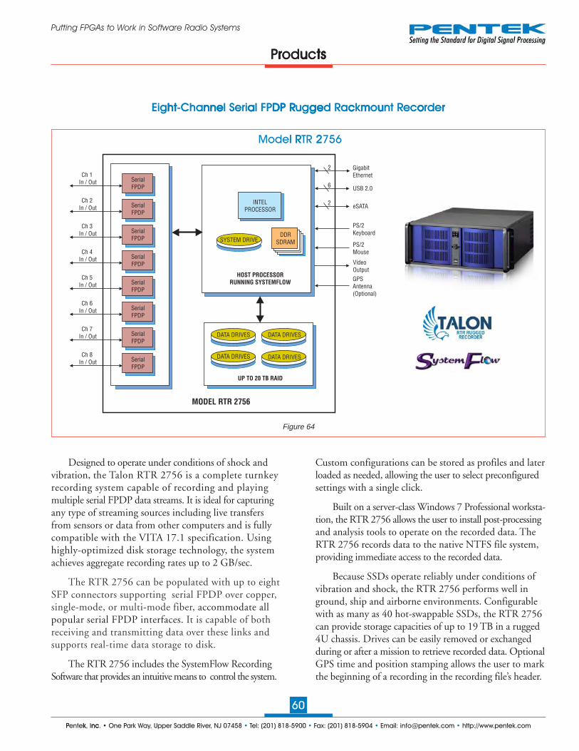
PP k nc entek, Inc. • One Park Way, Upper Saddle River, NJ 07458 • Tel: (201) 818-5900 • Fax: (201) 818-5904 • Email: [email protected] • http://www.pentek.com
60
Putting FPGAs to Work in Software Radio Systems
PPr u tsroductsr tsuroducts
l R 2 Model RTR 2756
thhtEight-Eight- a D Rnne P nne a DP RChannel Serial FPDP RChannel Serial FPDP R e g ge ugged Rugged R u c m c m u ackmount Rackmount R o ro recorderecorder
Figure 64
Ch 1In / Out Serial
FPDP
INTELPROCESSOR
SYSTEM DRIVEDDR
SDRAM
HOST PROCESSORRUNNING SYSTEMFLOW
UP TO 20 TB RAID
DATA DRIVES DATA DRIVES
DATA DRIVES DATA DRIVES
MODEL RTR 2756
USB 2.0
GigabitEthernet
PS/2Keyboard
PS/2Mouse
VideoOutput
2
6
GPSAntenna(Optional)
Ch 2In / Out Serial
FPDP
Ch 3In / Out Serial
FPDP
Ch 4In / Out Serial
FPDP
Ch 5In / Out Serial
FPDP
Ch 6In / Out Serial
FPDP
Ch 7In / Out Serial
FPDP
Ch 8In / Out Serial
FPDP
eSATA2
Designed to operate under conditions of shock andvibration, the Talon RTR 2756 is a complete turnkeyrecording system capable of recording and playingmultiple serial FPDP data streams. It is ideal for capturingany type of streaming sources including live transfersfrom sensors or data from other computers and is fullycompatible with the VITA 17.1 specification. Usinghighly-optimized disk storage technology, the systemachieves aggregate recording rates up to 2 GB/sec.
The RTR 2756 can be populated with up to eightSFP connectors supporting serial FPDP over copper,single-mode, or multi-mode fiber, accommodate allpopular serial FPDP interfaces. It is capable of bothreceiving and transmitting data over these links andsupports real-time data storage to disk.
The RTR 2756 includes the SystemFlow RecordingSoftware that provides an intuitive means to control the system.
Custom configurations can be stored as profiles and laterloaded as needed, allowing the user to select preconfiguredsettings with a single click.
Built on a server-class Windows 7 Professional worksta-tion, the RTR 2756 allows the user to install post-processingand analysis tools to operate on the recorded data. TheRTR 2756 records data to the native NTFS file system,providing immediate access to the recorded data.
Because SSDs operate reliably under conditions ofvibration and shock, the RTR 2756 performs well inground, ship and airborne environments. Configurablewith as many as 40 hot-swappable SSDs, the RTR 2756can provide storage capacities of up to 19 TB in a rugged4U chassis. Drives can be easily removed or exchangedduring or after a mission to retrieve recorded data. OptionalGPS time and position stamping allows the user to markthe beginning of a recording in the recording file’s header.

PP k nc entek, Inc. • One Park Way, Upper Saddle River, NJ 07458 • Tel: (201) 818-5900 • Fax: (201) 818-5904 • Email: [email protected] • http://www.pentek.com
61
Putting FPGAs to Work in Software Radio Systems
PP odu troductsodu troducts
PP e o m e m o entek SystemFlow Rentek SystemFlow R o e r ng e or ng ecording Sofecording Sof rt at artwaretware
Figure 65
Signal Viewer
Recorder Interface Hardware ConfigurationInterface
The Pentek SystemFlow® Recording Softwareprovides a rich set of function libraries and tools forcontrolling all Pentek RTS real-time data acquisitionand recording instruments. SystemFlow software allowsdevelopers to configure and customize system interfacesand behavior.
The Recorder Interface includes configuration,record, playback and status screens, each with intuitivecontrols and indicators. The user can easily move betweenscreens to set configuration parameters, control andmonitor a recording, play back a recorded signal andmonitor board temperatures and voltage levels.
The Hardware Configuration Interface providesentries for input source, center frequency, decimation, aswell as gate and trigger information. All parameterscontain limit-checking and integrated help to provide aneasier-to-use out-of-the-box experience.
The SystemFlow Signal Viewer includes a virtualoscilloscope and spectrum analyzer for signal monitoringin both the time and frequency domains. It is extremelyuseful for previewing live inputs prior to recording, andfor monitoring signals as they are being recorded to helpensure successful recording sessions. The viewer can alsobe used to inspect and analyze the recorded files afterthe recording is complete.
Advanced signal analysis capabilities include automaticcalculators for signal amplitude and frequency, secondand third harmonic components, THD (total harmonicdistortion) and SINAD (signal to noise and distortion).With time and frequency zoom, panning modes and dualannotated cursors to mark and measure points of interest,the SystemFlow Signal Viewer can often eliminate theneed for a separate oscilloscope or spectrum analyzer inthe field.

PP k nc entek, Inc. • One Park Way, Upper Saddle River, NJ 07458 • Tel: (201) 818-5900 • Fax: (201) 818-5904 • Email: [email protected] • http://www.pentek.com
62
Putting FPGAs to Work in Software Radio Systems
c oA l c nsApp icati sApplicationsp i tAp ca i sApplications
Figure 66
INTELPROCESSOR
SYSTEM DRIVEDDR
SDRAM
HOST PROCESSOR
UP TO 20 TB RAID
DATA DRIVES DATA DRIVES
DATA DRIVES DATA DRIVES
USB 2 0
GigabitEthernet
PS/2Keyboard
PS/2Mouse
VideoOutput
2
6
eSATA2
GPSAntenna
x8 PCIe
Input A
Input B
Output A
Output B
500 MHzA/D
500 MHzA/D
800 MHzD/A
800 MHzD/A
Pentek Cobalt 78651 PCIe Board
DUC
FPGAwith
2 Channelsof DDC
--2-2- nne onne oChannel SofChannel Sof r t a t ar tware Rtware Ra o Ra o Radio Radio R c i a P S s ed l c di a Pl S s eecording and Playback Systemecording and Playback System
Shown above is a 2-channel recording and playbacksystem utilizing the Pentek Cobalt 78651 PCIe board.The 78651 samples two input channels at up to 500 mega-samples per second, thereby accommodating inputsignals with up to 200 MHz bandwidth.
Factory-installed in the FPGA is a powerful 2-channelDDC (Digital Downconverter) IP core. Each DDC hasan independent 32-bit tuning frequency setting thatranges from DC to ƒs, where ƒs is the A/D samplingfrequency. Each DDC can have its own uniquedecimation setting, supporting as many as two differentoutput bandwidths for the board. Decimations can beprogrammed from 2 to 131,072 providing a wide range tosatisfy most applications.
The decimating filter for each DDC accepts aunique set of user-supplied 16-bit coefficients. The 80%default filters deliver an output bandwidth of 0.8*ƒs/N,where N is the decimation setting. The rejection ofadjacent-band components within the 80% outputbandwidth is better than 100 dB. Each DDC delivers acomplex output stream consisting of 24-bit I + 24-bit Qor 16-bit I + 16-bit Q samples at a rate of ƒs/N.
A TI DAC5688 DUC (Digital Upconverter) and D/Aaccepts a baseband real or complex data stream from theFPGA and provides that input to the upconvert, inter-polate and dual D/A stages.
When operating as a DUC, it interpolates and trans-lates real or complex baseband input signals to any IFcenter frequency up to 360 MHz. It delivers real orquadrature (I+Q) analog outputs to the dual 16-bit D/Aconverter. Analog output is through a pair of front panelSSMC connectors. If translation is disabled, theDAC5688 acts as a dual interpolating 16-bit D/A withoutput sampling rates up to 800 MHz.
Built on a Windows 7 Professional workstation withhigh performance Intel® CoreTM i7 processor this systemallows the user to install post processing and analysistools to operate on the recorded data. The system recordsdata to the native NTFS file system, providing immediateaccess to the recorded data.
Included with this system is Pentek’s SystemFlowrecording software. Optional GPS time and positionstamping allows the user to record this critical signalinformation.

PP k nc entek, Inc. • One Park Way, Upper Saddle River, NJ 07458 • Tel: (201) 818-5900 • Fax: (201) 818-5904 • Email: [email protected] • http://www.pentek.com
63
Putting FPGAs to Work in Software Radio Systems
c oA l t sApplications
Figure 67
INTELPROCESSOR
SYSTEM DRIVEDDR
SDRAM
HOST PROCESSOR
UP TO 20 TB RAID
DATA DRIVES DATA DRIVES
DATA DRIVES DATA DRIVES
USB 2 0
GigabitEthernet
PS/2Keyboard
PS/2Mouse
VideoOutput
2
6
eSATA2
GPSAntenna
x8 PCIe
x8 PCIe
Input A
Input B
Input C
Input D
200 MHzA/D
200 MHzA/D
200 MHzA/D
200 MHzA/D
FPGAwith
4 banks of8 Channel
DDC
Pentek Cobalt 78622 PCIe Board
Input A
Input B
Input C
Input D
200 MHzA/D
200 MHzA/D
200 MHzA/D
200 MHzA/D
FPGAwith
4 banks of8 Channel
DDC
Pentek Cobalt 78622 PCIe Board
--64-64- ne n nne Channel SofChannel Sof r t a t ar tware Rtware Ra o Ra o Radio Radio R sc i S ec i S s eecording Systemecording System
Each DDC delivers a complex output stream consist-ing of 24-bit I + 24-bit Q samples at a rate of ƒs/N. Anynumber of channels can be enabled within each bank,selectable from 0 to 8. Each bank includes an outputsample interleaver that delivers a channel-multiplexedstream for all enabled channels within a bank.
An internal timing bus provides all timing and synchro-nization required by the eight A/D converters. It includesa clock, two sync and two gate or trigger signals. An on-board clock generator receives an external sample clock.This clock can be used directly by the A/D or divided bya built-in clock synthesizer circuit.
Built on a Windows 7 Professional workstation withhigh performance Intel® CoreTM i7 processor this systemallows the user to install post processing and analysistools to operate on the recorded data. The system recordsdata to the native NTFS file system, providing immediateaccess to the recorded data.
Included with this system is Pentek’s SystemFlowrecording software. Optional GPS time and positionstamping allows the user to record this critical signalinformation.
Shown above is a 64-channel recording system utilizingtwo Pentek Cobalt 78662 PCIe boards. The 78662samples four input channels at up to 200 megasamplesper second, thereby accommodating input signals withup to 80 MHz bandwidth.
Factory-installed in the FPGA of each 78662 is apowerful DDC IP core containing 32 channels. Each ofthe 32 channels has an independent 32-bit tuningfrequency setting that ranges from DC to ƒs, where ƒs isthe A/D sampling frequency. All of the 8 channelswithin each bank share a common decimation settingthat can range from 16 to 8192, programmable in stepsof 8. For example, with a sampling rate of 200 MHz, theavailable output bandwidths range from 19.53 kHz to10.0 MHz. Each 8-channel bank can have its ownunique decimation setting supporting a different band-width associated with each of the four acquisition modules.
The decimating filter for each DDC bank acceptsa unique set of user-supplied 18-bit coefficients. The 80%default filters deliver an output bandwidth of 0.8*ƒs/N,where N is the decimation setting. The rejection ofadjacent-band components within the 80% outputbandwidth is better than 100 dB.

PP k nc entek, Inc. • One Park Way, Upper Saddle River, NJ 07458 • Tel: (201) 818-5900 • Fax: (201) 818-5904 • Email: [email protected] • http://www.pentek.com
64
Putting FPGAs to Work in Software Radio Systems
Figure 68
LL S na P S na P-Band Signal P-Band Signal Pr i e s mr e si mrocessing Systemrocessing System
p i tAp ca i sApplications
The Cobalt Model 78690 L-Band RF Tuner targetsreception and processing of digitally-modulated RFsignals such as satellite television and terrestrial wirelesscommunications. The 78690 requires only an antennaand a host computer to form a complete L-band SDRdevelopment platform.
This system receives L-Band signals between 925 MHzand 2175 MHz directly from an antenna. Signals abovethis range such as C Band, Ku Band and K band can bedownconverted to L-Band through an LNB (Low NoiseBlock) downconverter installed in the receiving antenna.
The Maxim Max2112 L-Band Tuner IC features alow-noise amplifier with programmable gain from 0 to65 dB and a synthesized local oscillator programmablefrom 925 to 2175 MHz. The complex analog mixertranslates the input signals down to DC. Basebandamplifiers provide programmable gain from 0 to 15 dBin steps of 1 dB. The bandwidth of the baseband lowpassfilters can be programmed from 4 to 40 MHz . TheMaxim IC accommodates full-scale input levels of -50 dBmto +10 dbm and delivers I and Q complex baseband outputs.
Analog Digital
Baseband IL-Band
x8 PCIe
LNA
Analog Local
Oscillator
Synthesizer
Q
Baseband AmpsAnalog Mixer
Analog Mixer
I
AnalogLowpass
FilterA/D
A/D
FPGA
VIRTEX 6
PC
WINDOWS
RF Input Baseband Q
MaximMAX2112
Pentek 78690 PCIe Board
LowpassFilter
Analog
The complex I and Q outputs are digitized by two200 MHz 16-bit A/D converters operating synchronously.
The Virtex-6 FPGA is a powerful resource forrecovering and processing a wide range of signalswhile supporting decryption, decoding, demodula-tion, detection, and analysis. It is ideal for interceptingor monitoring traffic in SIGINT and COMINTapplications. Other applications that benefit includemobile phones, GPS, satellite terminals, military telem-etry, digital video and audio in TV broadcasting satellites,and voice, video and data communications.
This L-Band signal processing system is ideal as afront end for government and military systems. Its smallsize adderesses space-limited applications. Ruggedizedoptions are also available from Pentek with the Models71690 XMC module and the 53690 OpenVPX board toaddress UAV applications and other severe environments.
Development support for this system is provided bythe Pentek ReadyFlow board support package for Windows,Linux and VxWorks. Also available is the Pentek GateFlowFPGA Design Kit to support custom algorithm development.

PP k nc entek, Inc. • One Park Way, Upper Saddle River, NJ 07458 • Tel: (201) 818-5900 • Fax: (201) 818-5904 • Email: [email protected] • http://www.pentek.com
65
Putting FPGAs to Work in Software Radio Systems
Figure 69
p i tAp ca i sApplications
8-8-8-8- n p nV e o m ng tC a l X m yC an l p nV X e m o m ng y tChannel OpenVPX Beamforming SystemChannel OpenVPX Beamforming System
Two Model 53661 boards are installed in slots 1 and2 of an OpenVPX backplane, along with a CPU boardin slot 3. Eight dipole antennas designed for receiving2.5 GHz signals feed RF Tuners containing low noiseamplifiers, local oscillators and mixers. The RF Tunerstranslate the 2.5 GHz antenna frequency signal downto an IF frequency of 50 MHz.
The 200 MHz 16-bit A/Ds digitize the IF signalsand perform further frequency downconversion to baseband,with a DDC decimation of 128. This provides I+Q complexoutput samples with a bandwidth of about 1.25 MHz. Phaseand gain coefficients for each channel are applied tosteer the array for directionality.
The CPU board in VPX slot 3 sends commandsand coefficients across the backplane over two x4 PCIelinks, or OpenVPX “fat pipes”.
The first four signal channels are processed in theupper left 53661 board in VPX slot 1, where the 4-channelbeamformed sum is propagated through the 4X AuroraSum Out link across the backplane to the 4X Aurora SumIn port on the second 53661 in slot 2. The 4-channel localsummation from the second 53661 is added to the propa-gated sum from the first board to form the complete 8-channelsum. This final sum is sent across the x4 PCIe link to theCPU card in slot 3.
Assignment of the three OpenVPX 4X links on theModel 53661 boards is simplified through the use of acrossbar switch which allows the 53661 to operate witha wide variety of different backplanes.
Because OpenVPX does not restrict the use of serialprotocols across the backplane links, mixed protocolarchitectures like the one shown are fully supported. ➤
VPX P1
Slot 1
EP02
EP01
DP01
FP C
VPX P1
Slot 2
VPX P1
Slot 3 CPU
EP02
EP01
DP01
FPC
x4 PCIe
x4 PCIe
200 MHz
16-bit A/D
DDC 4G + Phase
PCIe
x4
I/F
200 MHz16-bit A/D
200 MHz
16-bit A/D
200 MHz
16-bit A/D
AURORA
BEAMFORMSUMMATION
DDC 3
G + Phase
DDC 2G + Phase
DDC 1
G + Phase
4X Sum In
4X Sum Out
Model 53661
x4 PCIe
200 MHz
16-bit A/D
DDC 4
G + Phase
PCIe
x4
I/F
200 MHz16-bit A/D
200 MHz
16-bit A/D
200 MHz
16-bit A/D
AURORA
BEAMFORMSUMMATION
DDC 3
G + Phase
DDC 2
G + Phase
DDC 1
G + Phase
4X Sum In
4X Sum Out
x4 PCIe
Model 53661
RF Tuner
RF Tuner
RF Tuner
RF Tuner
RF Tuner
RF Tuner
RF Tuner
RF Tuner
FP B
FP A
DP01
DP02
OpenVPX
CPUBoard
VPXBACKPLANE
4X Aurora

PP k nc entek, Inc. • One Park Way, Upper Saddle River, NJ 07458 • Tel: (201) 818-5900 • Fax: (201) 818-5904 • Email: [email protected] • http://www.pentek.com
66
Putting FPGAs to Work in Software Radio Systems
p i tAp ca i sApplications
Figure 70
8-8-8-8- n nV X e o yC a l m D o s s eC an l nV X e m o D o sys eChannel OpenVPX Beamforming Demo systemChannel OpenVPX Beamforming Demo system
➤ The beamforming demo system is equipped with aControl Panel that runs under Windows on the CPUboard. It includes an automatic signal scanner to detectthe strongest signal frequency arriving from a testtransmitter. This frequency is centered around the50 MHz IF frequency of the RF downconverter. Oncethe frequency is identified, the eight DDCs are setaccordingly to bring that signal down to 0 Hz forsummation.
The control panel software also allows specifichardware settings for all of the parameters for the eightchannels including gain, phase, and sync delay.
An additional display shows the beam-formed pattern ofthe array. This display is formed by adjusting the phaseshift of each of the eight channels to provide maximumsensitivity across arrival angles from -90O to +90O
perpendicular to the plane of the array.
The classic 7-lobe pattern for an ideal 8-elementarray for a signal arriving at 0O angle (directly in front ofthe array) is shown above. Below the lobe pattern is apolar plot showing a single vector pointing to thecomputed angle of arrival. This is derived from identify-ing the lobe with the maximum response.
An actual plot of a real-life transmitter is also shownfor a source directly in front of the display. In this casethe perfect lobe pattern is affected by physical objects,reflections, cable length variations and minor differencesin the antennas. Nevertheless, the directional informationis computed quite well. As the signal source is moved leftand right in front of the array, the peak lobe moves withit, changing the computed angle of arrival.
This demo system is available online at Pentek. Ifyou are interested in viewing a live demonstration, pleaselet us know of your interest by clicking on this link:
Beamforming Demo.
Beamforming Demo Control Panel Theoretical 7-lobe Beamforming Patern Real-Life Beamforming Patern

PP k nc entek, Inc. • One Park Way, Upper Saddle River, NJ 07458 • Tel: (201) 818-5900 • Fax: (201) 818-5904 • Email: [email protected] • http://www.pentek.com
67
Putting FPGAs to Work in Software Radio Systems
● Communications Algorithms: DDC, DUC, demodu-lation, decoding, symbol recovery
● Beamforming: direction finding, phased arrayprocessing,diversity receivers
● Analysis: FFTs, decryption, statistical analysis● Triggering and Gating: radar aquisition and control● Memory control: DMA engines, circular buffers● Formatting and Packing: flexible data manipulation
for special I/O, packet extraction and formation● High-Speed Interfaces: switched serial fabric
interfaces, such as Serial RapidIO, PCI Express
Pentek offers a comprehensive array of VMEbusDSP boards featuring the AltiVec G4 PowerPC fromFreescale and the TMS320C6000 family of processorproducts from Texas Instruments.
On-board processor densities range from one toeight DSPs with many different memory and interfaceoptions available.
The Models 4205 and 4207 I/O processor boardsfeature the latest G4 PowerPCs, accept PMC mezzaninesand include built-in Fibre Channel interfaces.
The Models 4294 and 4295 processor boards featurefour MPC74xx G4 PowerPC processors utilizing theAltiVec vector processor capable of delivering severalGFLOPS of processing power.
The Models 4292 and 4293 processor boards featurethe Texas Instruments latest TMS320C6000 family offixed-point DSPs that represent a 10-fold increase inprocessing power over previous designs.
Once again, the ability of the system designer tofreely choose the most appropriate DSP processor foreach software radio application, facilitates systemrequirement changes and performance upgrades.
Full software development tools are available for work-stations running Windows and Linux with many differentdevelopment system configurations available.
V Eb d f d f V EbDSP Boards for VMEbusDSP Boards for VMEbus
S mmSummarS mmSummaryy
Figure 71
● Freescale Altivec G4PowerPC
● Texas InstrumentsC6000 DSPs
● Single, Dual, Quad andOctal Processor versions
● PMC, PMC/XMC, PCI,PCIe, and cPCI peripherals
● VME/VXS platforms
Figure 72
As we have seen, FPGAs are truly an integral part ofthe latest generation of software radio products.
Not only are they being used with traditional digitalsignal processing algorithms but also in the managementof data acquisition, buffering, triggering and timingaspects of high-performance real time systems.
With the addition of FPGA technology, dramaticincreases in system density have been coupled with asignificantly lower cost per channel. Furthermore,FPGA technology allows one to incorporate customalgorithms right at the front end of these systems.
Pentek offers not only a wide range of hardwareproducts featuring the latest FPGAs, but also the FPGAdevelopment resources and knowledgeable applicationsengineers to help you get the most out of these products.
We encourage you to contact your Pentek salesengineers today to discuss your system needs.
And be sure to visit our extensive web site for thelatest product and technical information.
A A FPGAs and SDRFPGAs and SDR

PP k nc entek, Inc. • One Park Way, Upper Saddle River, NJ 07458 • Tel: (201) 818-5900 • Fax: (201) 818-5904 • Email: [email protected] • http://www.pentek.com
68
Putting FPGAs to Work in Software Radio Systems
iLinksiLinks
More links on the next page ➤
The following links provide you with additional information about the Pentek productspresented in this handbook: just click on the model number. Links are also provided to otherhandbooks or catalogs that may be of interest in your software radio development projects.
o eModel e c iDescription PPage
7131 Multiband Receiver - PMC 177231 Multiband Receiver - 6U cPCI 177331 Multiband Receiver - 3U cPCI 177631A Multiband Receiver - PCI 175331 Multiband Receiver - 3U VPX 177141 Multiband Transceiver with Virtex-II Pro FPGA - PMC/XMC 187141-703 Conduction-cooled Multiband Transceiver with Virtex-II FPGA - PMC/XMC 187241 Multiband Transceiver with Virtex-II Pro FPGA - 6U cPCI 187341 Multiband Transceiver with Virtex-II Pro FPGA - 3U cPCI 187641 Multiband Transceiver with Virtex-II Pro FPGA - PCI 187741 Multiband Transceiver with Virtex-II Pro FPGA - Full-length PCIe 187841 Multiband Transceiver with Virtex-II Pro FPGA - Half-length PCIe 185341 Multiband Transceiver with Virtex-II Pro FPGA - 3U VPX 187141-420 Transceiver w. Dual Wideband DDC and Interpolation Filter - PMC/XMC 197241-420 Transceiver w. Dual Wideband DDC and Interpolation Filter - 6U cPCI 197341-420 Transceiver w. Dual Wideband DDC and Interpolation Filter - 3U cPCI 197641-420 Transceiver w. Dual Wideband DDC and Interpolation Filter - PCI 197741-420 Transceiver w. Dual Wideband DDC and Interpolation Filter - Full-length PCIe 197841-420 Transceiver w. Dual Wideband DDC and Interpolation Filter - Half-length PCIe 195341-420 Transceiver w. Dual Wideband DDC and Interpolation Filter - 3U VPX 197141-430 Transceiver w. 256-Channel Narrowband DDC - PMC/XMC 207241-430 Transceiver w. 256-Channel Narrowband DDC - 6U cPCI 207341-430 Transceiver w. 256-Channel Narrowband DDC - 3U cPCI 207641-430 Transceiver w. 256-Channel Narrowband DDC - PCI 207741-430 Transceiver w. 256-Channel Narrowband DDC - Full-length PCIe 207841-430 Transceiver w. 256-Channel Narrowband DDC - Half-length PCIe 205341-430 Transceiver w. 256-Channel Narrowband DDC - 3U VPX 207142 Multichannel Transceiver with Virtex-4 FPGAs - PMC/XMC 217242 Multichannel Transceiver with Virtex-4 FPGAs - 6U cPCI 217342 Multichannel Transceiver with Virtex-4 FPGAs - 3U cPCI 217642 Multichannel Transceiver with Virtex-4 FPGAs - PCI 217742 Multichannel Transceiver with Virtex-4 FPGAs - Full-length PCIe 217842 Multichannel Transceiver with Virtex-4 FPGAs - Half-length PCIe 215342 Multichannel Transceiver with Virtex-4 FPGAs - 3U VPX 217142-428 Multichannel Transceiver w. Four Multiband DDCs and Interpolation Filter - PMC/XMC 227242-428 Multichannel Transceiver w. Four Multiband DDCs and Interpolation Filter- 6U cPCI 227342-428 Multichannel Transceiver w. Four Multiband DDCs and Interpolation Filter- 3U cPCI 227642-428 Multichannel Transceiver w. Four Multiband DDCs and Interpolation Filter- PCI 227742-428 Multichannel Transceiver w. Four Multiband DDCs and Interpolation Filter- Full-length PCIe 227842-428 Multichannel Transceiver w. Four Multiband DDCs and Interpolation Filter- Half-length PCIe 225342-428 Multichannel Transceiver w. Four Multiband DDCs and Interpolation Filter- 3U VPX 22

PP k nc entek, Inc. • One Park Way, Upper Saddle River, NJ 07458 • Tel: (201) 818-5900 • Fax: (201) 818-5904 • Email: [email protected] • http://www.pentek.com
69
Putting FPGAs to Work in Software Radio Systems
iLinksiLinks
More links on the next page ➤
edModel s r t oDescription Page
7151 256-Channel DDC with Quad 200 MHz, 16-bit A/D - PMC 237251 256-Channel DDC with Quad 200 MHz, 16-bit A/D - 6U cPCI 237351 256-Channel DDC with Quad 200 MHz, 16-bit A/D - 3U cPCI 237651 256-Channel DDC with Quad 200 MHz, 16-bit A/D - PCI 237751 256-Channel DDC with Quad 200 MHz, 16-bit A/D - Full-length PCIe 237851 256-Channel DDC with Quad 200 MHz, 16-bit A/D - Half-length PCIe 235351 256-Channel DDC with Quad 200 MHz, 16-bit A/D - 3U VPX 237152 32-Channel DDC with Quad 200 MHz, 16-bit A/D - PMC 247252 32-Channel DDC with Quad 200 MHz, 16-bit A/D - 6U cPCI 247352 32-Channel DDC with Quad 200 MHz, 16-bit A/D - 3U cPCI 247652 32-Channel DDC with Quad 200 MHz, 16-bit A/D - PCI 247752 32-Channel DDC with Quad 200 MHz, 16-bit A/D - Full-length PCIe 247852 32-Channel DDC with Quad 200 MHz, 16-bit A/D - Half-length PCIe 245352 32-Channel DDC with Quad 200 MHz, 16-bit A/D - 3U VPX 247153 4-Channel DDC with Quad 200 MHz, 16-bit A/D - PMC/XMC 257253 4-Channel DDC with Quad 200 MHz, 16-bit A/D - 6U cPCI 257353 4-Channel DDC with Quad 200 MHz, 16-bit A/D - 3U cPCI 257653 4-Channel DDC with Quad 200 MHz, 16-bit A/D - PCI 257753 4-Channel DDC with Quad 200 MHz, 16-bit A/D - Full-length PCIe 257853 4-Channel DDC with Quad 200 MHz, 16-bit A/D - Half-length PCIe 255353 4-Channel DDC with Quad 200 MHz, 16-bit A/D - 3U VPX 257156 Dual SDR Transceiver, 400 MHz A/D, 800 MHz D/A, Virtex-5 FPGAs - PMC/XMC 267256 Dual SDR Transceiver, 400 MHz A/D, 800 MHz D/A, Virtex-5 FPGAs - 6U cPCI 267356 Dual SDR Transceiver, 400 MHz A/D, 800 MHz D/A, Virtex-5 FPGAs - 3U cPCI 267656 Dual SDR Transceiver, 400 MHz A/D, 800 MHz D/A, Virtex-5 FPGAs - PCI 267756 Dual SDR Transceiver, 400 MHz A/D, 800 MHz D/A, Virtex-5 FPGAs - Full-length PCIe 267856 Dual SDR Transceiver, 400 MHz A/D, 800 MHz D/A, Virtex-5 FPGAs - Half-length PCIe 265356 Dual SDR Transceiver, 400 MHz A/D, 800 MHz D/A, Virtex-5 FPGAs - 3U VPX 267158 Dual SDR Transceiver, 500 MHz A/D, 800 MHz D/A, Virtex-5 FPGAs - PMC/XMC 277258 Dual SDR Transceiver, 500 MHz A/D, 800 MHz D/A, Virtex-5 FPGAs - 6U cPCI 277358 Dual SDR Transceiver, 500 MHz A/D, 800 MHz D/A, Virtex-5 FPGAs - 3U cPCI 277658 Dual SDR Transceiver, 500 MHz A/D, 800 MHz D/A, Virtex-5 FPGAs - PCI 277758 Dual SDR Transceiver, 500 MHz A/D, 800 MHz D/A, Virtex-5 FPGAs - Full-length PCIe 277858 Dual SDR Transceiver, 500 MHz A/D, 800 MHz D/A, Virtex-5 FPGAs - Half-length PCIe 275358 Dual SDR Transceiver, 500 MHz A/D, 800 MHz D/A, Virtex-5 FPGAs - 3U VPX 2771620 3-Channel 200 MHz A/D, DUC, 2-Channel 800 MHz D/A, Virtex-6 FPGA - XMC 2878620 3-Channel 200 MHz A/D, DUC, 2-Channel 800 MHz D/A, Virtex-6 FPGA - PCIe 2853620 3-Channel 200 MHz A/D, DUC, 2-Channel 800 MHz D/A, Virtex-6 FPGA - 3U VPX 2872620 3-Channel 200 MHz A/D, DUC, 2-Channel 800 MHz D/A, Virtex-6 FPGA - 6U cPCI 2873620 3-Channel 200 MHz A/D, DUC, 2-Channel 800 MHz D/A, Virtex-6 FPGA - 3U cPCI 2874620 6-Channel 200 MHz A/D, DUC, 4-Channel 800 MHz D/A, Two Virtex-6 FPGAs - 6U cPCI 28

PP k nc entek, Inc. • One Park Way, Upper Saddle River, NJ 07458 • Tel: (201) 818-5900 • Fax: (201) 818-5904 • Email: [email protected] • http://www.pentek.com
70
Putting FPGAs to Work in Software Radio Systems
iLinksiLinks
More links on the next page ➤
d lModel s or tDescription P eage71621 3-Channel 200 MHz A/D, DUC, 2-Channel 800 MHz D/A, Installed IP Cores - XMC 2978621 3-Channel 200 MHz A/D, DUC, 2-Channel 800 MHz D/A, Installed IP Cores - PCIe 2953621 3-Channel 200 MHz A/D, DUC, 2-Channel 800 MHz D/A, Installed IP Cores - 3U VPX 2972621 3-Channel 200 MHz A/D, DUC, 2-Channel 800 MHz D/A, Installed IP Cores - 6U cPCI 2973621 3-Channel 200 MHz A/D, DUC, 2-Channel 800 MHz D/A, Installed IP Cores - 3U cPCI 2974621 4-Channel 200 MHz A/D, DUC, 4-Channel 800 MHz D/A, Installed IP Cores - 6U cPCI 3978630 1 GHz A/D, 1 GHz D/A, Virtex-6 FPGA - PCIe 3071630 1 GHz A/D, 1 GHz D/A, Virtex-6 FPGA - XMC 3053630 1 GHz A/D, 1 GHz D/A, Virtex-6 FPGA - 3U VPX 3072630 1 GHz A/D, 1 GHz D/A, Virtex-6 FPGA - 6U cPCI 3073630 1 GHz A/D, 1 GHz D/A, Virtex-6 FPGA - 3U cPCI 3074630 Two 1 GHz A/Ds, Two 1 GHz D/As, Two Virtex-6 FPGAs - 6U cPCI 3072640 1-Channel 3.6 GHz and 2-Channel 1.8 GHz, 12-bit A/D, Virtex-6 FPGA - 6U cPCI 3173640 1-Channel 3.6 GHz and 2-Channel 1.8 GHz, 12-bit A/D, Virtex-6 FPGA - 3U cPCI 3174640 2-Channel 3.6 GHz and 4-Channel 1.8 GHz, 12-bit A/D, Virtex-6 FPGAs - 6U cPCI 3171640 1-Channel 3.6 GHz and 2-Channel 1.8 GHz, 12-bit A/D, Virtex-6 FPGA - XMC 3178640 1-Channel 3.6 GHz and 2-Channel 1.8 GHz, 12-bit A/D, Virtex-6 FPGA - PCIe 3153640 1-Channel 3.6 GHz and 2-Channel 1.8 GHz, 12-bit A/D, Virtex-6 FPGA - 3U VPX 3153650 2-Channel 500 MHz A/D, DUC, 2-Channel 800 MHz D/A, Virtex-6 FPGA - 3U VPX 3271650 2-Channel 500 MHz A/D, DUC, 2-Channel 800 MHz D/A, Virtex-6 FPGA - XMC 3278650 2-Channel 500 MHz A/D, DUC, 2-Channel 800 MHz D/A, Virtex-6 FPGA - PCIe 3272650 2-Channel 500 MHz A/D, DUC, 2-Channel 800 MHz D/A, Virtex-6 FPGA - 6U cPCI 3273650 2-Channel 500 MHz A/D, DUC, 2-Channel 800 MHz D/A, Virtex-6 FPGA - 3U cPCI 3274650 4-Channel 500 MHz A/D, DUC, 4-Channel 800 MHz D/A, Two Virtex-6 FPGAs - 6U cPCI 3272651 2-Channel 500 MHz A/D, with DDCs, DUC, 2-Channel 800 MHz D/A, Virtex-6 FPGA - 6U cPCI 3373651 2-Channel 500 MHz A/D, with DDCs, DUC, 2-Channel 800 MHz D/A, Virtex-6 FPGA - 3U cPCI 3374651 2-Channel 500 MHz A/D, with DDCs, DUCs, 2-Channel 800 MHz D/A, Virtex-6 FPGA- 6U cPCI 3371651 2-Channel 500 MHz A/D, with DDCs, DUC, 2-Channel 800 MHz D/A, Virtex-6 FPGA - XMC 3378651 2-Channel 500 MHz A/D, with DDCs, DUC, 2-Channel 800 MHz D/A, Virtex-6 FPGA - PCIe 3353651 2-Channel 500 MHz A/D, with DDCs, DUC, 2-Channel 800 MHz D/A, Virtex-6 FPGA - 3U VPX 3371660 4-Channel 200 MHz 16-bit A/D with Virtex-6 FPGA - XMC 3478660 4-Channel 200 MHz 16-bit A/D with Virtex-6 FPGA - PCIe 3453660 4-Channel 200 MHz 16-bit A/D with Virtex-6 FPGA - 3U VPX 3472660 4-Channel 200 MHz 16-bit A/D with Virtex-6 FPGA - 6U cPCI 3473660 4-Channel 200 MHz 16-bit A/D with Virtex-6 FPGAs - 3U cPCI 3474660 8-Channel 200 MHz 16-bit A/D with Two Virtex-6 FPGAs - 6U cPCI 3471661 4-Channel 200 MHz 16-bit A/D with Installed IP Cores - XMC 3578661 4-Channel 200 MHz 16-bit A/D with Installed IP Cores - PCIe 3553661 4-Channel 200 MHz 16-bit A/D with Installed IP Cores - 3U VPX 3572661 4-Channel 200 MHz 16-bit A/D with Installed IP Cores - 6U cPCI 3573661 4-Channel 200 MHz 16-bit A/D with Installed IP Cores - 3U cPCI 3574661 8-Channel 200 MHz 16-bit A/D with Installed IP Cores - 6U cPCI 35
PP k nc entek, Inc. • One Park Way, Upper Saddle River, NJ 07458 • Tel: (201) 818-5900 • Fax: (201) 818-5904 • Email: [email protected] • http://www.pentek.com
71
Putting FPGAs to Work in Software Radio Systems
iLinksiLinks
MoModel D ie c iDescription PPaage
78662 4-Channel 200 MHz 16-bit A/D with Installed IP Cores - PCIe 3671662 4-Channel 200 MHz 16-bit A/D with Installed IP Cores - XMC 3653662 4-Channel 200 MHz 16-bit A/D with Installed IP Cores - 3U VPX 3672662 4-Channel 200 MHz 16-bit A/D with Installed IP Cores - 6U cPCI 3673662 4-Channel 200 MHz 16-bit A/D with Installed IP Cores - 3U cPCI 3674662 8-Channel 200 MHz 16-bit A/D with Installed IP Cores - 6U cPCI 3671670 4-Channel 1.25 GHz D/A with DUC, Virtex-6 FPGA - XMC 3778670 4-Channel 1.25 GHz D/A with DUC, Virtex-6 FPGA - PCIe 3753670 4-Channel 1.25 GHz D/A with DUC, Virtex-6 FPGA - 3U VPX 3772670 4-Channel 1.25 GHz D/A with DUC, Virtex-6 FPGA - 6U cPCI 3773670 4-Channel 1.25 GHz D/A with DUC, Virtex-6 FPGA - 3U cPCI 3774670 8-Channel 1.25 GHz D/A with DUCs, and Two Virtex-6 FPGAs - 6U cPCI 3753690 L-Band RF Tuner with 2-Channel 200 MHz A/D and Virtex-6 FPGA - 3U VPX 3871690 L-Band RF Tuner with 2-Channel 200 MHz A/D and Virtex-6 FPGA - XMC 3878690 L-Band RF Tuner with 2-Channel 200 MHz A/D and Virtex-6 FPGA - PCIe 3872690 L-Band RF Tuner with 2-Channel 200 MHz A/D and Virtex-6 FPGA - 6U cPCI 3873690 L-Band RF Tuner with 2-Channel 200 MHz A/D and Virtex-6 FPGA - 3U cPCI 3874690 Dual L-Band RF Tuner with 4-Channel 200 MHz A/D and Two Virtex-6 FPGAs - 6U cPCI 3871760 4-Channel 200 MHz 16-bit A/D with Virtex-7 FPGA - XMC 3978760 4-Channel 200 MHz 16-bit A/D with Virtex-7 FPGA - PCIe 3953760 4-Channel 200 MHz 16-bit A/D with Virtex-7 FPGA - 3U VPX 3972760 4-Channel 200 MHz 16-bit A/D with Virtex-7 FPGA - 6U cPCI 3973760 4-Channel 200 MHz 16-bit A/D with Virtex-7 FPGA - 3U cPCI 3974760 8-Channel 200 MHz 16-bit A/D with Two Virtex-7 FPGAs - 6U cPCI 396821-422 215 MHz, 12-bit A/D with Wideband DDCs - VME/VXS 406822-422 Dual 215 MHz, 12-bit A/D with Wideband DDCs - VME/VXS 416826 Dual 2 GHz 10-bit A/D - VME/VXS 426890 2.2 GHz Clock, Sync and Gate Distribution Board - VME 436891 System Synchronizer and Distribution Board - VME 447190 Multifrequency Clock Synthesizer - PMC 457290 Multifrequency Clock Synthesizer - 6U cPCI 457390 Multifrequency Clock Synthesizer - 3U cPCI 457690 Multifrequency Clock Synthesizer - PCI 457790 Multifrequency Clock Synthesizer - Full-length PCIe 457890 Multifrequency Clock Synthesizer - Half-length PCIe 455390 Multifrequency Clock Synthesizer - 3U VPX 457191 Programmable Multifrequency Clock Synthesizer - PMC 467291 Programmable Multifrequency Clock Synthesizer - 6U cPCI 467391 Programmable Multifrequency Clock Synthesizer - 3U cPCI 467691 Programmable Multifrequency Clock Synthesizer - PCI 467791 Programmable Multifrequency Clock Synthesizer - Full-length PCIe 467891 Programmable Multifrequency Clock Synthesizer - Half-length PCIe 465391 Programmable Multifrequency Clock Synthesizer - 3U VPX 46

PPPPPentek, Inc.entek, Inc.entek, Inc.entek, Inc.entek, Inc. • One Park Way, Upper Saddle River, NJ 07458 • Tel: (201) 818-5900 • Fax: (201) 818-5904 • Email: [email protected] • http://www.pentek.com
7272727272
Putting FPGAs to Work in Software Radio Systems
Click here Software Defined Radio HandbookClick here Critical Techniques for High-Speed A/D Converters in Real-Time Systems HandbookClick here High-Speed Switched Serial Fabrics Improve System Design HandbookClick here High-Speed, Real-Time Recording Systems HandbookClick here Onyx Virtex-7 and Cobalt Virtex-6 Product CatalogClick here Pentek Product Catalog
ModelModelModelModelModel DescriptionDescriptionDescriptionDescriptionDescription PPPPPageageageageage
7192 High-Speed Synchronizer and Distribution Board - PMC/XMC 477892 High-Speed Synchronizer and Distribution Board - PCIe 475392 High-Speed Synchronizer and Distribution Board - 3U VPX 477292 High-Speed Synchronizer and Distribution Board - 6U cPCI 477392 High-Speed Synchronizer and Distribution Board - 3U cPCI 477492 High-Speed Synchronizer and Distribution Board - 6U cPCI 477893 System Synchronizer and Distribution Board - PCIe 489190 Clock and Sync Generator for I/O Modules - Rackmount 499192 High-Speed System Synchronizer Unit - Rackmount 50RTS 2706 Eight-Channel RF/IF 200 MS/sec Rackmount Recorder 51RTS 2709 Ultra Wideband One- or Two-Channel RF/IF, 3.2 GS/sec Rackmount Recorder 52RTS 2715 Two-Channel 10 Gigabit Ethernet Rackmount Recorder 53RTS 2716 Eight-Channel Serial FPDP Rackmount Recorder 54RTR 2726 Four-Channel RF/IF 200 MS/sec Rugged Portable Recorder 55RTR 2736 Eight-Channel Serial FPDP Rugged Portable Recorder 56RTR 2746 Eight-Channel RF/IF 200 MS/sec Rugged Rackmount Recorder 57RTR 2749 Ultra Wideband One- or Two-Channel RF/IF, 3.2 GS/sec Rugged Rackmount Recorder 58RTR 2755 Two-Channel 10 Gigabit Ethernet Rugged Rackmount Recorder 59RTR 2756 Eight-Channel Serial FPDP Rugged Rackmount Recorder 60— Pentek SystemFlow Recording Software 61
Handbooks, Catalogs and BrochuresHandbooks, Catalogs and BrochuresHandbooks, Catalogs and BrochuresHandbooks, Catalogs and BrochuresHandbooks, Catalogs and Brochures
LinksLinksLinksLinksLinks