purepath digital audio six-channel pwm processor … · absolute maximum ratings dissipation...
TRANSCRIPT

1FEATURES
TAS5086
www.ti.com ................................................................................................................................................... SLES131C–FEBRUARY 2005–REVISED JUNE 2008
PurePath Digital™ AUDIO SIX-CHANNEL PWM PROCESSOR– Full Six-Channel Input and Output Mapping
23• Audio Input/Output – Selectable DC Blocking Filters– Automatic Master Clock Rate and Data • PWM Processing
Sample Rate Detection – 8× Oversampling With Fourth-Order Noise– Four Serial Audio Inputs (Eight Channels) Shaping at 44.1, 48 kHz; 4× Oversampling
at 88.2, 96 kHz; 2× Oversampling at 176.4,– Support for 32-, 44.1-, 48-, 88.2-, 96-, 176.4-,192 kHz; and 12× Oversampling at 32 kHzand 192-kHz Sampling Rates
– ≥105-dB Dynamic Range– Data Formats: 16-, 20-, or 24-Bit Input Data;(TAS5086+TAS5186)Left-Justified, Right-Justified, and I2S
– THD < 0.06% (TAS5086 Only)– 64- or 48-fS Bit-Clock Rate– 20-Hz–20-kHz Flat Noise Floor for 44.1-, 48-,– 128-, 192-, 256-, 384-, and 512-fS Master
88.2-, 96-, 176.4- and 192-kHz Data RatesClock Rates (Up to a Maximum of 50 MHz)– Digital De-Emphasis for 32-kHz, 44.1-kHz– Six PWM Audio Output Channels
and 48-kHz Data Rates– Any Output Channel Can be Mapped to Any– Intelligent AM Interference AvoidanceOutput Pin
System Provides Clear AM Reception– Supports Single-Ended and Bridge-Tied– Optimized PWM Sequence for Click- andLoads
Popless Start and Stop– I2S Serial Audio Output– Optimized PWM Sequence for Charging of• Audio Processing
AC-Coupling Capacitors in Single-Ended– Volume Control Range of 48 dB to –100 dB Configurations– Master Volume Control from 24 dB to –100 – Adjustable Modulation Limit From 93.8% to
dB in 0.5-dB Increments 99.2%– Six Individual Channel Volume Controls • General Features
With 24-dB to –100-dB Attenuation in– Automated Operation With Easy-to-Use0.5-dB Increments
Control Interface– Serial Output Can Be Produced by
– I2C Serial Control Slave InterfaceDownmix of 5.1-Channel Input or Fourth– Control Interface Operational WithoutSerial Input
MCLK– 5.1-Channel Downmix to 2.1 or 3.1 PWM– Single 3.3-V Power SupplyOutput Speaker System– 38-Pin TSSOP Package– Integrated Bass Management
– Two Programmable Biquads in SubwooferChannel
1
Please be aware that an important notice concerning availability, standard warranty, and use in critical applications of TexasInstruments semiconductor products and disclaimers thereto appears at the end of this data sheet.
2PurePath Digital is a trademark of Texas Instruments.3All other trademarks are the property of their respective owners.
PRODUCTION DATA information is current as of publication date. Copyright © 2005–2008, Texas Instruments IncorporatedProducts conform to specifications per the terms of the TexasInstruments standard warranty. Production processing does notnecessarily include testing of all parameters.

DESCRIPTION
TAS5086
SLES131C–FEBRUARY 2005–REVISED JUNE 2008 ................................................................................................................................................... www.ti.com
These devices have limited built-in ESD protection. The leads should be shorted together or the device placed in conductive foamduring storage or handling to prevent electrostatic damage to the MOS gates.
The TAS5086 is a six-channel digital pulse-width modulator (PWM) that provides both advanced performanceand a high level of system integration. The TAS5086 is designed to interface seamlessly with most audio digitalsignal processors and MPEG decoders, accepting a wide range of input data and clock formats.
The TAS5086 drives six channels of speakers in either single-ended or bridge-tied load configurations thataccept a 1N + 1 interface format. The TAS5086 also supports 2N + 1 power stages with the use of someexternal logic (e.g., TAS5112). Stereo line out in I2S format is available with either a pass-through signal (SDIN4)or an internal downmix.
The TAS5086 uses AD modulation operating at a 384-kHz switching rate for 32-, 44.1-, 48-, 88.2-, 96-, 176.4-,and 192-kHz data. The 8× oversampling, combined with the 4th-order noise shaper, provides a broad, flat noisefloor and excellent dynamic range from 20 Hz to 20 kHz.
The TAS5086 is only an I2C slave device, which always receives MCLK, SCLK, and LRCLK from other systemcomponents. The TAS5086 accepts clock rates of 128, 192, 256, 384, and 512 fS. The TAS5086 accepts a 64-fSmaster clock for 176.4-kHz and 192-kHz data.
The TAS5086 accepts a 64-fS bit clock for all data rates. The TAS5086 also can accept a 48-fS SCLK rate forMCLK ratios of 192 fS and 384 fS.
The TAS5086 is composed of five functional blocks.• Power supply• Clock, PLL, and serial data interface• Serial control interface• Device control• PWM section
For detailed application information, see the Using the PurePath Digital PWM Processor application report(SLEA046).
Figure 1 shows the functional structure of the TAS5086.
2 Submit Documentation Feedback Copyright © 2005–2008, Texas Instruments Incorporated
Product Folder Link(s): TAS5086

Chan.1 − 6
1− 5
SDIN1SDIN2SDIN3SDIN4
SDA
SCL
PWM1
PWM2
PWM3
PWM4
PWM5
PWM6
VALID1
DVDDDVSS
DVSS_ESDVR_DIG
VR_ANAVR_OSC
AVDDAVSS_PLL
SDOUT
MCLKSCLK
LRCLKPLLFLTPPLLFLTM
HFCLKOSCFLT
OSC_RES
1 LF
2 RF
3 LS
4 RS
5 C
1− 6
L’
R’
L’
R’
(L’+R’) / 2
VALID2
1 − 5
Ch1−6
6
6
6
6
6
6
SDIN4
SDIN4
Downmix
PWMControl
PDNRESET
MUTE
VREG_EN
BKNDERR
Channel Six ProcessingBass Management
B0080-01
PowerSupply
SerialData
Interface
ChannelSelector
Block
MUX
MUX
Down−mix
Clock Rate/Error
Detectionand PLL
SerialControl
Interface
SystemControl MUX I2S Serial
Output
MUX
MUX MUX
Vol PWM
MUX
MUX
MUX
MUX
MUX
(L’+R’)/2
TAS5086
www.ti.com ................................................................................................................................................... SLES131C–FEBRUARY 2005–REVISED JUNE 2008
Figure 1. TAS5086 Functional Block Diagram
Copyright © 2005–2008, Texas Instruments Incorporated Submit Documentation Feedback 3
Product Folder Link(s): TAS5086

ABSOLUTE MAXIMUM RATINGS
DISSIPATION RATINGS
RECOMMENDED OPERATING CONDITIONS
ELECTRICAL CHARACTERISTICS
TAS5086
SLES131C–FEBRUARY 2005–REVISED JUNE 2008 ................................................................................................................................................... www.ti.com
over operating free-air temperature range (unless otherwise noted) (1)
DVDD and DVD_ESD –0.3 V to 3.6 VSupply voltage
AVDD –0.3 V to 3.6 V3.3-V-digital input –0.5 V to DVDD + 0.5 V
Input voltage5-V-tolerant (2) digital input –0.5 V to 6 V
Input clamp current, IIK (VI < 0 or VI > 1.8 V) ±20 mAOutput clamp current, IOK (VO < 0 or VO > 1.8 V) ±20 mAOperating free-air temperature 0°C to 70°CStorage temperature range, Tstg –65°C to 150°C
(1) Stresses beyond those listed under “absolute ratings” may cause permanent damage to the device. These are stress ratings only, andfunctional operation of the device at these or any other conditions beyond those indicated under “recommended operation conditions”are not implied. Exposure to absolute-maximum conditions for extended periods may affect device reliability.
(2) 5-V tolerant inputs are RESET, PDN, MUTE, SCLK, LRCLK, MCLK, SDA, and SCL.
TA ≤ 25°C DERATING FACTOR TA = 70°C TA = 85°CPACKAGE POWER RATING ABOVE TA = 25°C POWER RATING POWER RATINGDBT 817.16 mW 10.214 mW/C 357.5 mW 204.29 mW
over operating free-air temperature range (unless otherwise noted)
MIN NOM MAX UNITDigital supply voltage DVDD 3 3.3 3.6 VAnalog supply voltage AVDD 3 3.3 3.6 V
VIH High-level input voltage 3.3-V TTL, 5-V tolerant 2 VVIL Low-level input voltage 3.3-V TTL, 5-V tolerant 0.8 VTA Operating ambient-air temperature range 0 25 70 °C
over operating free-air temperature range (unless otherwise noted)
PARAMETER TEST CONDITIONS MIN TYP MAX UNITVOH High-level output voltage 3.3-V TTL and 5-V (1) tolerant IOH = –4 mA 2.4 VVOL Low-level output voltage 3.3-V TTL and 5-V (1) tolerant IOL = 4 mA 0.5 VIOZ High-impedance output current 3.3-V TTL 20 µA
3.3-V TTL VI = VIL 1IIL Low-level input current µA
5-V tolerant (2) VI = 0 V, DVDD = 3 V 13.3-V TTL VI = VIH 1
IIH High-level input current µA5-V tolerant (2) VI = 5.5 V, DVDD = 3 V 20
fS = 48 kHz 140fS = 96 kHz 150
Digital supply voltage, DVDD mAfS = 192 kHz 155
IDD Input supply currentPower down 8Normal 20
Analog supply voltage, AVDD mAPower down 2
(1) 5-V-tolerant outputs are SCL and SDA(2) 5-V-tolerant inputs are SDA, SCL, RESET, PDN, MUTE, HP_SEL, SCLK, LRCLK, MCLK, SDIN1, SDIN2, SDIN3, and SDIN4.
4 Submit Documentation Feedback Copyright © 2005–2008, Texas Instruments Incorporated
Product Folder Link(s): TAS5086

Serial Audio Port
th1
tsu1
tsu2
th2
SCLK(Input)
LRCLK(Input)
SDIN1SDIN2SDIN3
T0026-01
TAS5086 Pin-Related Characteristics of the SDA and SCL I/O Stages for F/S-Mode I2C-Bus
TAS5086
www.ti.com ................................................................................................................................................... SLES131C–FEBRUARY 2005–REVISED JUNE 2008
Serial audio port slave mode over recommended operating conditions (unless otherwise noted)
PARAMETER TEST CONDITIONS MIN TYP MAX UNITfSCLKIN SCLK input frequency CL = 30 pF, SCLK = 64 fS 2.048 12.288 MHztsu1 Setup time, LRCLK to SCLK rising edge 10 nsth1 Hold time, LRCLK from SCLK rising edge 10 nstsu2 Setup time, SDIN to SCLK rising edge 10 nsth2 Hold time, SDIN from SCLK rising edge 10 ns
LRCLK frequency 32 48 192 kHzSCLK duty cycle 40% 50% 60%LRCLK duty cycle 40% 50% 60%
SCLKSCLK rising edges between LRCLK rising edges 64 64 edgesLRCLK clock edge with respect to the falling edge of SCLK–1/4 1/4SCLK period
Figure 2. Slave Mode Serial Data Interface Timing
DevicesSTANDARD MODE FAST MODE
PARAMETER TEST CONDITIONS UNITMIN MAX MIN MAX
VIL LOW-level input voltage –0.5 0.3 VDD –0.5 0.3 VDD VVIH HIGH-level input voltage 0.7 VDD 0.7 VDD VVhys Hysteresis of Schmitt-trigger inputs N/A N/A 0.05 VDD V
LOW-level output voltage (open drain orVOL1 3-mA sink current 0 0.4 Vopen collector)Bus capacitance from 10 pF 7 + 0.1 Cbtof Output fall time from VIHmin to VILmax 250 250 nsto 400 pF (1)
tSP Pulse duration of spikes suppressed (2) N/A N/A 0 30 nsIi Input current, each I/O pin –30 30 –30 (3) 30 (3) µACi Capacitance, each I/O pin 10 10 pF
(1) Cb = capacitance of one bus line in pF. The output fall time is faster than the standard I2C specification.(2) SCL and SDA have a 30-ns glitch filter.(3) The I/O pins of fast-mode devices must not obstruct the SDA and SDL lines if VDD is switched off.
Copyright © 2005–2008, Texas Instruments Incorporated Submit Documentation Feedback 5
Product Folder Link(s): TAS5086

TAS5086 Bus-Related Characteristics of the SDA and SCL I/O Stages for F/S-Mode I2C-Bus
SDA
SCL
tf tSU-DAT tHD-STA tr
tBUF
tSU-STO
P S
tSP
tSU-STA
Sr
tHIGH
tHD-DAT
tLOW
tr
tHD-STA
S
tf
T0114-01
TAS5086
SLES131C–FEBRUARY 2005–REVISED JUNE 2008 ................................................................................................................................................... www.ti.com
DevicesAll values are referred to VIHmin and VILmax (see TAS5086 Pin-Related Characteristics of the SDA and SCL I/O Stages forF/S-Mode I2C-Bus Devices).
A
STANDARD MODE FAST MODEPARAMETER TEST CONDITIONS UNIT
MIN MAX MIN MAXfSCL SCL clock frequency 0 100 0 400 kHz
Hold time (repeated) START condition.tHD-STA After this period, the first clock pulse is 4 0.6 µs
generated.tLOW LOW period of the SCL clock 4.7 1.3 µstHIGH HIGH period of the SCL clock 4 0.6 µstSU-STA Setup time for repeated START 4.7 0.6 µstSU-DAT Data setup time 250 100 µstHD-DAT Data hold time (1) (2) 0 3.45 0 0.9 µstr Rise time of both SDA and SCL 1000 7 + 0.1 Cb
(3) 500 (4) nstf Fall time of both SDA and SCL 300 7 + 0.1 Cb
(3) 300 nstSU-STO Setup time for STOP condition 4 0.6 µstBUF Bus free time between a STOP and 4.7 1.3 µs
START conditionCb Capacitive loads for each bus line 400 400 pF
Noise margin at the LOW level for eachVnL 0.1 VDD 0.1 VDD Vconnected device (including hysteresis)Noise margin at the HIGH level for eachVnH 0.2 VDD 0.2 VDD Vconnected device (including hysteresis)
(1) Note that SDA does not have the standard I2C specification 300-ns hold time and that SDA must be valid by the rising and falling edgesof SCL. TI recommends that a 3.3-kΩ pullup resistor be used to avoid potential timing issues.
(2) A fast-mode I2C-bus device can be used in a standard-mode I2C-bus system, but the requirement tSU-DAT ≥ 250 ns must then be met.This is automatically the case if the device does not stretch the LOW period of the SCL signal. If such a device does stretch the LOWperiod of the SCL signal, it must output the next data bit to the SDA line tr-max + tSU-DAT = 1000 + 250 = 1250 ns (according to thestandard-mode I2C bus specification) before the SCL line is released.
(3) Cb = total capacitance of one bus line in pF.(4) Rise time varies with pullup resistor.
Figure 3. Start and Stop Conditions Timing Waveforms
6 Submit Documentation Feedback Copyright © 2005–2008, Texas Instruments Incorporated
Product Folder Link(s): TAS5086

Recommended I2C Pullup Resistors
B0099-05
TAS5086 ExternalMicrocontroller
VI(SDA)
5 V
IP IP
VI(SCL)
SDA
RP RP
SCL
B0100-05
TAS5086 ExternalMicrocontroller
VI
5 V
IP
SDAor
SCL
RS
(2)
VS
(1)
RS
(2)
RP
TAS5086
www.ti.com ................................................................................................................................................... SLES131C–FEBRUARY 2005–REVISED JUNE 2008
It is recommended that the I2C pullup resistors RP be 3.3 kΩ (see Figure 4). If a series resistor is in the circuit(see Figure 5), then the series resistor RS should be less than or equal to 300 Ω.
Figure 4. I2C Pullup Circuit (With No Series Resistor)
(1) VS = 5 × RS/(RS + RP). When driven low, VS << VIL requirements.(2) RS ≤ 300 Ω
Figure 5. I2C Pullup Circuit (With Series Resistor)
Copyright © 2005–2008, Texas Instruments Incorporated Submit Documentation Feedback 7
Product Folder Link(s): TAS5086
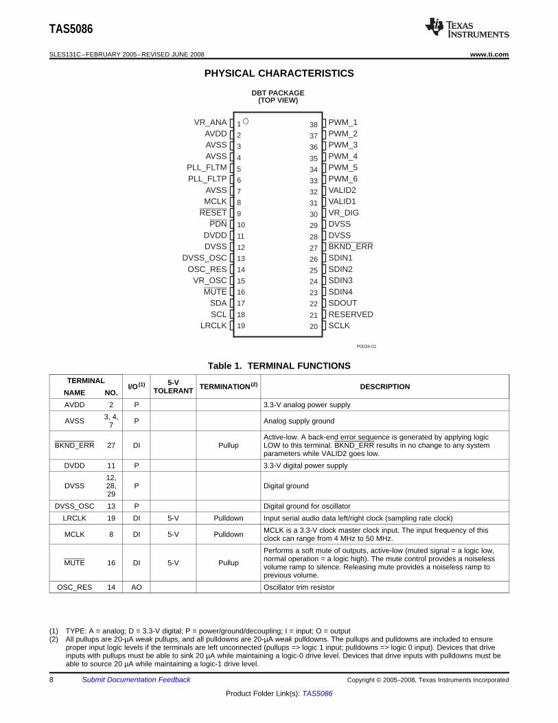
PHYSICAL CHARACTERISTICS
1
2
3
4
5
6
7
8
9
10
11
12
13
14
15
16
17
18
19
38
37
36
35
34
33
32
31
30
29
28
27
26
25
24
23
22
21
20
VR_ANAAVDDAVSSAVSS
PLL_FLTMPLL_FLTP
AVSSMCLK
RESETPDN
DVDDDVSS
DVSS_OSCOSC_RES
VR_OSCMUTE
SDASCL
LRCLK
PWM_1PWM_2PWM_3PWM_4PWM_5PWM_6VALID2VALID1VR_DIGDVSSDVSSBKND_ERRSDIN1SDIN2SDIN3SDIN4SDOUTRESERVEDSCLK
DBT PACKAGE(TOP VIEW)
P0034-01
TAS5086
SLES131C–FEBRUARY 2005–REVISED JUNE 2008 ................................................................................................................................................... www.ti.com
Table 1. TERMINAL FUNCTIONSTERMINAL 5-VI/O (1) TERMINATION (2) DESCRIPTIONTOLERANTNAME NO.
AVDD 2 P 3.3-V analog power supply3, 4,AVSS P Analog supply ground7
Active-low. A back-end error sequence is generated by applying logicBKND_ERR 27 DI Pullup LOW to this terminal. BKND_ERR results in no change to any system
parameters while VALID2 goes low.DVDD 11 P 3.3-V digital power supply
12,DVSS 28, P Digital ground
29DVSS_OSC 13 P Digital ground for oscillator
LRCLK 19 DI 5-V Pulldown Input serial audio data left/right clock (sampling rate clock)MCLK is a 3.3-V clock master clock input. The input frequency of thisMCLK 8 DI 5-V Pulldown clock can range from 4 MHz to 50 MHz.Performs a soft mute of outputs, active-low (muted signal = a logic low,normal operation = a logic high). The mute control provides a noiselessMUTE 16 DI 5-V Pullup volume ramp to silence. Releasing mute provides a noiseless ramp toprevious volume.
OSC_RES 14 AO Oscillator trim resistor
(1) TYPE: A = analog; D = 3.3-V digital; P = power/ground/decoupling; I = input; O = output(2) All pullups are 20-µA weak pullups, and all pulldowns are 20-µA weak pulldowns. The pullups and pulldowns are included to ensure
proper input logic levels if the terminals are left unconnected (pullups => logic 1 input; pulldowns => logic 0 input). Devices that driveinputs with pullups must be able to sink 20 µA while maintaining a logic-0 drive level. Devices that drive inputs with pulldowns must beable to source 20 µA while maintaining a logic-1 drive level.
8 Submit Documentation Feedback Copyright © 2005–2008, Texas Instruments Incorporated
Product Folder Link(s): TAS5086

TAS5086
www.ti.com ................................................................................................................................................... SLES131C–FEBRUARY 2005–REVISED JUNE 2008
Table 1. TERMINAL FUNCTIONS (continued)TERMINAL 5-VI/O (1) TERMINATION (2) DESCRIPTIONTOLERANTNAME NO.
Power down, active-low. PDN powers down all logic, stops all clocks, andperforms a soft stop whenever a logic low is applied. The internalparameters are preserved through a power-down cycle, as long as RESETPDN 10 DI 5-V Pullup is not active. The duration for system recovery from power down is 100ms. When released, PDN powers up all logic, starts all clocks, andperforms a soft start that returns to the previous configuration.
PLL_FLTM 5 AO PLL negative inputPLL_FLTP 6 AI PLL positive inputPWM_ 1 38 DO PWM 1 outputPWM_ 2 37 DO PWM 2 outputPWM_ 3 36 DO PWM 3 outputPWM_ 4 35 DO PWM 4 outputPWM_ 5 34 DO PWM 5 outputPWM_ 6 33 DO PWM 6 output
RESERVED 21 – RESERVED (connect to ground)A system reset is generated by applying a logic low to this terminal.RESET is an asynchronous control signal that restores the TAS5086 to itsdefault conditions, sets the VALID2 output low, and places the PWM in theRESET 9 DI 5-V Pullup hard-mute (M) state. Master volume is immediately set to full attenuation.On the release of RESET, if PDN is high, the system performs a 4–5-msdevice initialization and sets the volume at mute.
SCL 18 DI 5-V I2C serial control clock inputSerial audio data clock (shift clock). SCLKIN is the serial audio port (SAP)SCLK 20 DI 5-V Pulldown input data bit clock.
SDA 17 DIO 5-V I2C serial control data interface input/outputSerial audio data 1 input is one of the serial data input ports. SDIN1SDIN1 26 DI Pulldown supports four discrete (stereo) data formats.Serial audio data 2 input is one of the serial data input ports. SDIN2SDIN2 25 DI Pulldown supports four discrete (stereo) data formats.Serial audio data 3 input is one of the serial data input ports. SDIN3SDIN3 24 DI Pulldown supports four discrete (stereo) data formats.Serial audio data 4 input is one of the serial data input ports. SDIN4SDIN4 23 DI Pulldown supports four discrete (stereo) data formats.Serial audio data 1 output is the only serial data output port. SDOUTSDOUT 22 DI supports I2S format only.Soft start valid. Output indicating validity of soft-start PWM output,VALID1 31 DO active-high
VALID2 32 DO Output indicating validity of PWM outputs, active-high.Voltage reference for analog supply, 1.8 V. A pinout of the internallyregulated 1.8-V power. A 0.1-µF, low-ESR capacitor should be connectedVR_ANA 1 P between this terminal and AVSS_PLL. This terminal must not be used topower external devices.Voltage reference for digital PWM core supply, 1.8 V. A pinout of theinternally regulated 1.8-V power used by digital PWM core logic. A 0.1-µF,VR_DIG 30 P low-ESR (3) capacitor should be connected between this terminal andDVSS_PWM. This terminal must not be used to power external devices.Voltage reference for analog supply, 1.8 V. A pinout of the internallyregulated 1.8-V power. A 0.1-µF, low-ESR (3) capacitor should beVR_OSC 15 P connected between this terminal and AVSS_PLL. This terminal must notbe used to power external devices.
(3) If desired, low-ESR capacitance values can be implemented by paralleling two or more ceramic capacitors of equal value. Parallelingcapacitors of equal value provides an extended high-frequency supply decoupling. This approach avoids the potential of producingparallel resonance circuits that have been observed when paralleling capacitors of different values.
Copyright © 2005–2008, Texas Instruments Incorporated Submit Documentation Feedback 9
Product Folder Link(s): TAS5086
DETAILED DESCRIPTION
POWER SUPPLY
CLOCK, ERROR RATE DETECTION, AND PLL
OSCILLATOR TRIM
TAS5086
SLES131C–FEBRUARY 2005–REVISED JUNE 2008 ................................................................................................................................................... www.ti.com
The TAS5086 power-supply section contains regulators that provide analog and digital regulated power forvarious sections of the TAS5086. The analog supply supports the analog PLL while digital supplies support thedigital PLL, the digital audio processor, the pulse width modulator, and the output control (reclocker). Thepower-supply section is enabled via VREG_EN.
This module provides the timing and serial data interface for the TAS5086.The TAS5086 is a clock slave device. It accepts MCLK, SCLK, and LRCLK.The TAS5086 supports 64-fS MCLK for the 176.4-kHz and 192-kHz data rates.The TAS5086 accepts a 64-fS SCLK rate for all MCLK ratios and a 48-fS SCLK rate for MCLK ratios of 192 fSand 384 fS.TAS5086 checks to verify that SCLK is a specific value of 64 fS or 48 fS.The TAS5086 supports a 1-fS LRCLK.The timing relationship of these clocks to SDIN[1:4] and SDOUT is shown in subsequent sections.The clock section uses MCLK or the internal oscillator clock (when MCLK is unstable or absent) to produce a196-MHz PLL output.
The TAS5086 can auto-detect and set the internal clock control logic to the appropriate settings for thefrequencies of 32 kHz, normal speed (44.1 or 48 kHz), double speed (88.2 kHz or 96 kHz), and quad speed(176.4 kHz or 192 kHz). The automatic sample rate detection can be disabled and the values set via I2C.
The TAS5086 also supports an AM interference-avoidance mode during which the clock rate is adjusted, inconcert with the PWM sample rate converter, to produce a PWM output at 7-fS, 8-fS, or 9-fS.
The sample rate must be set manually during AM interference avoidance and when de-emphasis is enabled.
The TAS5086 uses an internal oscillator time base to provide reference timing information for the followingfunctions:• MCLK, SCLK, and LRCLK error detection• I2C communication when power is first applied to the device• Automatic data-rate detection and setting (32 kHz, normal, double, and quad speed)• Automatic MCLK rate detection and setting (64, 128, 192, 256, 384, and 512 fS)
The TAS5086 PWM processor contains an internal oscillator for PLL reference. This reduces system costbecause an external reference is not required. After each power up or reset, a oscillator trim is needed; see theOscillator Trim Register (0x1B) section for a detailed procedure.
10 Submit Documentation Feedback Copyright © 2005–2008, Texas Instruments Incorporated
Product Folder Link(s): TAS5086

SERIAL DATA INTERFACE
I2C SERIAL CONTROL INTERFACE
B0048-01
(L'+R')/2
Format
Channel1–6
Channel1–6
1–5
1–5
Down-mix
SDIN1
PWM_1
PWM_2
PWM_3
PWM_4
PWM_5
PWM_6
1 LF
2 RF
3 LS
4 RS
5 C
0x20
0x21
0x25
L'
R'
L'
R'0x04
SDIN2SDIN3
SDIN4
SDIN4
MUX
0x21
Ch-6 Processing
MUX
MUX
Downmix
SDIN4
PWM MUX
SDOUT
I S2
0x07– 0x0D
0x03
VOL
SEL
VOL
VOL
VOL
VOL
MUX
TAS5086
www.ti.com ................................................................................................................................................... SLES131C–FEBRUARY 2005–REVISED JUNE 2008
Serial data is input on SDIN1, SDIN2, SDIN3, and SDIN4. The PWM outputs and downmix are derived fromSDIN1, SDIN2, and SDIN3. SDIN4 is a selectable pass-through signal that is available at SDOUT as an I2Soutput. The TAS5086 accepts 32-, 44.1-, 48-, 88.2-, 96-, 176.4-, and 192-kHz serial data in 16-, 20-, or 24-bit,left-justified, right-justified, and I2S serial data formats.
Serial data is output on SDOUT. The SDOUT data format is I2S 24-bit at the same data rate as the input. TheSDOUT output is synchronized to use the SCLK and LRCLK signals. There is a 1- to 2.5-LRCLK frame delayfrom the input data to the output data, depending on the input serial data format. The SDOUT output has noI2C-controllable functions. It is always operational.
The parameters of this clock and serial data interface input format are I2C configurable.
The TAS5086 has an I2C serial control slave interface to receive commands from a system controller. The serialcontrol interface supports both normal-speed (100-kHz) and high-speed (400-kHz) operations without wait states.As an added feature, this interface operates even if MCLK is absent.
The serial control interface supports both single-byte and multi-byte read and write operations for status registersand the general control registers associated with the PWM.
The I2C interface supports a special mode that permits I2C write operations to be broken up into multiple-datawrite operations that are multiples of 4 data bytes. These are 6-, 10-, 14-, 18-, ... etc., -byte write operations thatare composed of a device address, read/write bit, subaddress, and any multiple of 4 bytes of data. This permitsthe system to write large register values incrementally without blocking other I2C transactions.
Figure 6 shows the data flow and control through the TAS5086. The major I2C registers are shown above eachapplicable block (e.g., 0x04 is the serial data format control register).
Figure 6. TAS5086 Data Flow Diagram With I2C Registers
Copyright © 2005–2008, Texas Instruments Incorporated Submit Documentation Feedback 11
Product Folder Link(s): TAS5086

Channel-6 Processing Section
B0050-01
0x21
0x0D
BQ1 (G)
0x23Gain-
CompensatedBiquad
0x24Low-Pass
Biquad
VOL
10 dB
Bass Management
Ch 1–5
Ch 6 Sub
From Downmix (L’+R’)/2
S
BQ1 BQ2MUX
PWM Section
TAS5086
SLES131C–FEBRUARY 2005–REVISED JUNE 2008 ................................................................................................................................................... www.ti.com
Channel 6 has processing features that are directly applicable to the subwoofer channel.
Figure 7. Channel-6 Processing Block Diagram
The TAS5086 has six channels of high-performance digital PWM modulators that are designed to drive switchingoutput stages (back ends) in both single-ended (SE) and H-bridge (bridge-tied load) configurations. TheTAS5086 device uses noise-shaping and sophisticated error correction algorithms to achieve high powerefficiency and high-performance digital audio reproduction. The TAS5086 uses a fourth-order noise shaper toprovide >105-dB SNR performance from 20 Hz to 20 kHz.
The TAS5086 PWM interface is described by using the following notation:PN + V
whereP = number of PWM signals per channelN = number of channelsV = total number of valid signals used to reset the power stage
For example, the TAS5086 initial interface format means that there is 1 PWM signal per channel (N = 6) and 1valid signal is used to reset the power stages. The shorthand notation to describe this is 1N+1.
The PWM section accepts 24-bit PCM data from the serial data interface and outputs six PWM audio outputchannels to drive 1N+1 single-ended and BTL power stages.
The PWM interface supports:• TAS5186 in BTL or SE mode without any external glue logic, uses 1N+1 signaling.• TAS5142 in BTL or SE mode without any external glue logic, uses 1N+1 signaling.• TAS5111 SE without any external glue logic, and with a pulldown on the output, uses 1N+1 signaling.• TAS5111 BTL or TAS5112 BTL with one inverter per BTL channel of glue logic and a pulldown on the output,
uses 1N+1 signaling from TAS5086, 2N+1 input to TAS5111/12.• TAS5112 SE (with external glue logic)
See the application schematics for an example of the TAS5086 with the TAS5186 and the TAS5086 withTAS5112 SE and TAS5111 SE.
The TAS5086 has input multiplexers that allow any of the input channels to be routed to any PWM channel andoutput multiplexers to enable any PWM output to be routed to any PWM output pin.
12 Submit Documentation Feedback Copyright © 2005–2008, Texas Instruments Incorporated
Product Folder Link(s): TAS5086

Transitions Between Shutdown and Playing
Output Stage
PSU
VPP
GND
IN
IN
VPP
GND
PWM
TAS5086
OUT
OUT
S0269-01
TAS5086
www.ti.com ................................................................................................................................................... SLES131C–FEBRUARY 2005–REVISED JUNE 2008
It also has individual channel dc-blocking filters that are enabled by default.
Individual channel de-emphasis filters for 32, 44.1, and 48 kHz are included and can be enabled and disabled.
There is also a two-channel downmix result that can be output on SDOUT (I2S format). This result also can besent to the left and right front channels (channels 1 and 2) and/or to the center and subwoofer (channels 5 and 6)as well.
A mixer on the subwoofer channel supports bass management configuration 1.
PWM output characteristics• Up to 8× oversampling• 12× at fS = 32 kHz, 8× at fS = 48 kHz, 4× at fS = 96 kHz, 2× at fS = 192 kHz• Fourth-order noise shaping• ≥105-dB dynamic range, 0–20 kHz (TAS5086 + TAS5186 system measured at speaker terminals)• THD < 0.06% (measured at TAS5086 outputs)• Adjustable maximum modulation limit of 93.8% to 99.2%
The TAS5086 outputs are switching all the time with the noise shaper active. Mute is acheived by inputting azero into the noise shaper, with the noise shaper running and the output still switching. By using this approach,the transitions between off and operation is avoided. The only exception is shutdown of surround channels asdescribed in the Surround Register (0x19) section.
Futhermore, the TAS5086 is designed to drive a load in single-ended and bridge-tied-load configurations. Theprinciple in the SE and BTL configurations is shown in Figure 8 and Figure 9. In both situations, care must betaken to ensure correct start-up sequences which charge the bootstrap capacitor and do not produce audibleartifacts; the TAS5086 is designed to do that.
Figure 8. BTL Filter Configuration
The SE configuration presents an additional challenge in order for starting up quietly. The second terminal of theloudspeaker is connected to a split capacitor between power and ground. The advantage of this circuitly is that itprovides some degree of power-supply ripple rejection. The problem related to the split capacitor is that thevoltage over it must be controlled when the modulator starts (i.e., when the power stage output goes out of highimpedance state) to avoid a click in the speaker.
Copyright © 2005–2008, Texas Instruments Incorporated Submit Documentation Feedback 13
Product Folder Link(s): TAS5086

PSU
VPP
GND
INPWM
TAS5086
OUT
S0270-01
Power Stage
TAS5086
SLES131C–FEBRUARY 2005–REVISED JUNE 2008 ................................................................................................................................................... www.ti.com
Figure 9. SE Filter Configuration
The TAS5086 supports two mechanisms for controlling the split-capacitor midpoint.
In the extra half-bridge scheme (the TAS5186 power stage is an example of this) an additional half-bridge isstarted and brought to a 50-percent duty cycle, i.e., a situation where the average voltage of the half-bridge isequal to the voltage which must be applied to the split-capacitor midpoint to start up without clicks in the speaker.A resistor per channel is connected between the extra half-bridge and each midpoint for the split capacitors. Thesplit capacitors are charged through this resistor. This approach requires an extra VALID pin on the modulator tocontrol the extra half-bridge, therefore the 1N+2 interface. Figure 10 shows the topology of the extra half-bridge.In some situations, a channel configured in BTL can be used to charge the split capacitor instead of the extrahalf-bridge. This is shown in Figure 11.
The mid-Z scheme charges the split capacitor through the loudspeaker. In order to do this without audibleartifacts the charge current must be limited. This is done by applying a start sequence which charges the outputstate between low, high and high-Z. Because the ouput stage is in high-Z in a part of the sequence, the resultingoutput impedance can be brought to a level suitable for charging the split capacitors without audible artifacts.This solution does not require external components, as shown in Figure 9. Not all power stages are compatiblewith the mid-Z scheme, double-check the power-stage data sheet for compabitility. The PWM start register(0x18) programs the TAS5086 for mid-Z or the standard low-Z start sequence.
14 Submit Documentation Feedback Copyright © 2005–2008, Texas Instruments Incorporated
Product Folder Link(s): TAS5086

S0271-01
Power Stage
Extra Half-Bridge
PSU
VPP
GND
IN
IN
VPP
GND
PWM
TAS5086
OUT
OUT
RES
RES
ValidSS
Valid
Power Stage SE
RES
ValidSS
Valid
Power Stage BTL
PSU
VPP
IN
RES
IN
VPP
GND
GND
PWM
PWM
TAS5086
OUT+
OUT–
OUT
S0272-01
TAS5086
www.ti.com ................................................................................................................................................... SLES131C–FEBRUARY 2005–REVISED JUNE 2008
Figure 10. Split-Capacitor Charging With Extra Half-Bridge
Figure 11. Split-Capacitor Charging With BTL Subwoofer
Copyright © 2005–2008, Texas Instruments Incorporated Submit Documentation Feedback 15
Product Folder Link(s): TAS5086

Reset Timing (RESET)
tw(RESET)
Earliest timethat M-State
could be exited
RESET
M-State
tr(DMSTATE) < 200 ns
tr(I2C_ready)
Start system
tr(run)
Determine SCLK rateand MCLK ratio. Enable via I 2C.
T0029-03
Power-Down (PDN) Timing
PDN
M-State
tsutp(DMSTATE) < 1 ms
T0030-02
Back-End Error (BKND_ERR)
TAS5086
SLES131C–FEBRUARY 2005–REVISED JUNE 2008 ................................................................................................................................................... www.ti.com
Control-signal parameters over recommended operating conditions (unless otherwise noted)
PARAMETER MIN TYP MAX UNITtr(DMSTATE) Time to M-STATE low 370 nstw(RESET) Pulse duration, RESET active 400 None nstr(I2C_ready) Time to enable I2C 3 mstr(run) Device start-up time 10 ms
NOTE: Because a crystal time base is used, the system determines the CLK rates. Once the data rate and master clock ratioare determined, the system outputs audio if a master volume command is issued.
Figure 12. Reset Timing
Control-signal parameters over recommended operating conditions (unless otherwise noted). Note that PDN does not clearI2C registers.
PARAMETER MIN TYP MAX UNITtp(DMSTATE) Time to M-STATE low 300 µs
Number of MCLKs preceding the release of PDN 5tsu Device start-up time 120 ms
Figure 13. Power-Down Timing
Control-signal parameters over recommended operating conditions (unless otherwise noted)
16 Submit Documentation Feedback Copyright © 2005–2008, Texas Instruments Incorporated
Product Folder Link(s): TAS5086

BKND_ERR
M-Stateor
Valid2
tw(ER)
NormalOperation
NormalOperation
T0031-02
tp(valid_low)
tp(valid_high) tp(valid_high)
tp(valid_low) tp(valid_low)
Mute Timing (MUTE)
td(VOL)
VOLUME
MUTE
NormalOperation
M-State NormalOperation
td(VOL)T0032-01
TAS5086
www.ti.com ................................................................................................................................................... SLES131C–FEBRUARY 2005–REVISED JUNE 2008
Control-signal parameters over recommended operating conditions (unless otherwise noted)
PARAMETER MIN TYP MAX UNITtw(ER) Pulse duration, BKND_ERR active 350 None nstp(valid_low) <100 µstp(valid_high) I2C programmable to be between 1 to 10 ms –25 25 % of interval
Figure 14. Error Recovery Timing
Control-signal parameters over recommended operating conditions (unless otherwise noted). Note that MUTE does not stopPWM switching; it stops the noise shaper, and therefore has less noise.
PARAMETER MIN TYP MAX UNITtd(VOL) Volume ramp time Defined by rate setting(1) ms
(1) See the Volume Control Register (0x0E) section.
Figure 15. Mute Timing
Copyright © 2005–2008, Texas Instruments Incorporated Submit Documentation Feedback 17
Product Folder Link(s): TAS5086

SERIAL INTERFACE CONTROL AND TIMING
I2S TIMING
23 22
SCLK
32 Clks
LRCLK (Note Reversed Phase) Left Channel
24-Bit Mode
9 8 5 4 1 0
19 18
20-Bit Mode
5 4 1 0
16-Bit Mode
1 015 14
MSB LSB
23 22
SCLK
32 Clks
Right Channel
9 8 5 4 1 0
19 18 5 4 1 0
1 015 14
MSB LSB
2-Channel I 2S (Philips Format) Stereo Input/Output
T0034-04
TAS5086
SLES131C–FEBRUARY 2005–REVISED JUNE 2008 ................................................................................................................................................... www.ti.com
I2S timing uses LRCLK to define when the data being transmitted is for the left channel and when it is for theright channel. LRCLK is low for the left channel and high for the right channel. A bit clock running at 64 fS is usedto clock in the data. A delay of one bit clock occurs from the time the LRCLK signal changes state to the first bitof data on the data lines. The data is written MSB-first and is valid on the rising edge of the bit clock. TheTAS5086 masks unused trailing data bit positions.
Figure 16. I2S 64-fS Format
18 Submit Documentation Feedback Copyright © 2005–2008, Texas Instruments Incorporated
Product Folder Link(s): TAS5086

23 22
SCLK
24 Clks
LRCLK Left Channel
24-Bit Mode
1
19 18
20-Bit Mode
16-Bit Mode
15 14
MSB LSB
24 Clks
Right Channel
2-Channel I S (Philips Format) Stereo Input/Output (24-Bit Transfer Word Size)2
T0092-01
3 25 49 817 16
1 0
0
4513 12
1 09 8
23 22
SCLK
1
19 18
15 14
MSB LSB
3 25 49 817 16
1 04513 12
1 09 8
LEFT-JUSTIFIED
TAS5086
www.ti.com ................................................................................................................................................... SLES131C–FEBRUARY 2005–REVISED JUNE 2008
Figure 17. I2S 48-fS Format
Left-justified (LJ) timing uses LRCLK to define when the data being transmitted is for the left channel and when itis for the right channel. LRCLK is high for the left channel and low for the right channel. A bit clock running at 64fS is used to clock in the data. The first bit of data appears on the data lines at the same time LRCLK toggles.The data is written MSB-first and is valid on the rising edge of the bit clock. The TAS5086 masks unused trailingdata bit positions.
Copyright © 2005–2008, Texas Instruments Incorporated Submit Documentation Feedback 19
Product Folder Link(s): TAS5086

23 22
SCLK
32 Clks
LRCLK
Left Channel
24-Bit Mode
1
19 18
20-Bit Mode
16-Bit Mode
15 14
MSB LSB
32 Clks
Right Channel
2-Channel Left-Justified Stereo Input
T0034-02
459 8
145
1
0
0
0
23 22 1
19 18
15 14
MSB LSB
459 8
145
1
0
0
0
SCLK
23 22
SCLK
24 Clks
LRCLK
Left Channel
24-Bit Mode
1
19 18
20-Bit Mode
16-Bit Mode
15 14
MSB LSB
24 Clks
Right Channel
2-Channel Left-Justified Stereo Input (24-Bit Transfer Word Size)
T0092-02
459 817 16
14513 12
19 8
0
0
0
21
17
13
23 22
SCLK
1
19 18
15 14
MSB LSB
459 817 16
14513 12
19 8
0
0
0
21
17
13
TAS5086
SLES131C–FEBRUARY 2005–REVISED JUNE 2008 ................................................................................................................................................... www.ti.com
Figure 18. Left-Justified 64-fS Format
Figure 19. Left-Justified 48-fS Format
20 Submit Documentation Feedback Copyright © 2005–2008, Texas Instruments Incorporated
Product Folder Link(s): TAS5086

Right-Justified
23 22
SCLK
32 Clks
LRCLK
Left Channel
24-Bit Mode
1
20-Bit Mode
16-Bit Mode
15 14
MSB LSB
SCLK
32 Clks
Right Channel
2-Channel Right-Justified (Sony Format) Stereo Input
T0034-03
19 18
119 18
1
0
0
0
15 14
15 14 23 22 1
15 14
MSB LSB
19 18
119 18
1
0
0
0
15 14
15 14
TAS5086
www.ti.com ................................................................................................................................................... SLES131C–FEBRUARY 2005–REVISED JUNE 2008
Right-justified (RJ) timing uses LRCLK to define when the data being transmitted is for the left channel and whenit is for the right channel. LRCLK is high for the left channel and low for the right channel. A bit clock running at64 fS is used to clock in the data. The first bit of data appears on the data 8 bit-clock periods (for 24-bit data)after LRCLK toggles. In RJ mode, the LSB of data always is clocked by the last bit clock before LRCLKtransitions. The data is written MSB-first and is valid on the rising edge of bit clock. The TAS5086 masks unusedleading data bit positions.
Figure 20. Right-Justified 64-fS Format
Copyright © 2005–2008, Texas Instruments Incorporated Submit Documentation Feedback 21
Product Folder Link(s): TAS5086

23 22
SCLK
24 Clks
LRCLK
Left Channel
24-Bit Mode
1
20-Bit Mode
16-Bit Mode
15 14
MSB LSB
SCLK
24 Clks
Right Channel
MSB
2-Channel Right-Justified Stereo Input (24-Bit Transfer Word Size)
T0092-03
519 18
1519 18
15
0
0
0
2
2
2
6
6
6
15 14
15 14 23 22 1
15 14
519 18
1519 18
15
0
0
0
2
2
2
6
6
6
15 14
15 14
LSB
I2C SERIAL CONTROL INTERFACE
GENERAL I2C OPERATION
TAS5086
SLES131C–FEBRUARY 2005–REVISED JUNE 2008 ................................................................................................................................................... www.ti.com
Figure 21. Right-Justified 48-fS Bit Format
The TAS5086 has a bidirectional Inter IC (I2C) interface that is compatible with the I2C bus protocol and supportsboth single- and multiple-byte write and read operations. The control interface is used to program the registers ofthe device and to read device status.
The TAS5086 supports wait-state insertions by other I2C devices on the bus. However, the TAS5086 performs allI2C operations without I2C wait cycles.
The TAS5086 supports standard-mode I2C bus operation (100 kHz maximum) and fast I2C bus operation (400kHz maximum).
The I2C bus employs two signals, SDA (data) and SCL (clock), to communicate between integrated circuits in asystem. Data is transferred on the bus serially, one bit at a time. The address and data are transferred in byte(8-bit) format with the most-significant bit (MSB) transferred first. In addition, each byte transferred on the bus isacknowledged by the receiving device with an acknowledge bit. Each transfer operation begins with the masterdevice driving a start condition on the bus and ends with the master device driving a stop condition on the bus.The bus uses transitions on the data terminal (SDA) while the clock is high to indicate start and stop conditions.A high-to-low transition on SDA indicates a start and a low-to-high transition indicates a stop. Normal data-bittransitions must occur within the low time of the clock period. These conditions are shown in Figure 22. Themaster generates the 7-bit slave address and the read/write (R/W) bit to open communication with anotherdevice and then wait for an acknowledge condition. The TAS5086 holds SDA low during the acknowledge clockperiod to indicate an acknowledgment. When this occurs, the master transmits the next byte of the sequence.Each device is addressed by a unique 7-bit slave address plus R/W bit (1 byte). All compatible devices share thesame signals via a bidirectional bus using a wired-AND connection. An external pullup resistor must be used forthe SDA and SCL signals to set the HIGH level for the bus.
22 Submit Documentation Feedback Copyright © 2005–2008, Texas Instruments Incorporated
Product Folder Link(s): TAS5086

7-Bit Slave AddressR/W
8-Bit Register Address (N)A8-Bit Register Data For
Address (N)
Start Stop
SDA
SCL
7 6 5 4 3 2 1 0 7 6 5 4 3 2 1 0 7 6 5 4 3 2 1 0 7 6 5 4 3 2 1 0
A8-Bit Register Data For
Address (N)A A
T0035-01
SINGLE- AND MULTIPLE-BYTE TRANSFERS
SINGLE-BYTE WRITE
TAS5086
www.ti.com ................................................................................................................................................... SLES131C–FEBRUARY 2005–REVISED JUNE 2008
Figure 22. Typical I2C Sequence
An unlimited number of bytes can be transmitted between start and stop conditions. When the last wordtransfers, the master generates a stop condition to release the bus. A generic data transfer sequence is shown inFigure 22.
The 7-bit address for the TAS5086 is 0011 011.
The serial control interface supports both single-byte and multiple-byte read/write operations for status registersand the general control registers associated with the PWM. However, for the DAP data processing registers, theserial control interface supports only multiple-byte (4-byte) read/write operations.
During multiple-byte read operations, the TAS5086 responds with data, a byte at a time, starting at thesubaddress assigned, as long as the master device continues to respond with acknowledges. If a particularsubaddress does not contain 32 bits, the unused bits are read as logic 0.
During multiple-byte write operations, the TAS5086 compares the number of bytes transmitted to the number ofbytes that are required for each specific subaddress. If a write command is received for a biquad subaddress, theTAS5086 expects to receive five 32-bit words. If fewer than five 32-bit data words have been received when astop command (or another start command) is received, the data received is discarded. Similarly, if a writecommand is received for a mixer coefficient, the TAS5086 expects to receive one 32-bit word.
Supplying a subaddress for each subaddress transaction is referred to as random I2C addressing. The TAS5086also supports sequential I2C addressing. For write transactions, if a subaddress is issued, followed by data forthat subaddress and the 15 subaddresses that follow, a sequential I2C write transaction has taken place, and thedata for all 16 subaddresses is successfully received by the TAS5086. For I2C sequential write transactions, thesubaddress then serves as the start address and the amount of data subsequently transmitted, before a stop orstart is transmitted, determines how many subaddresses are written. As was true for random addressing,sequential addressing requires that a complete set of data be transmitted. If only a partial set of data is written tothe last subaddress, the data for the last subaddress is discarded. However, all other data written is accepted;just the incomplete data is discarded.
As shown is Figure 23, a single-byte data write transfer begins with the master device transmitting a startcondition, followed by the I2C device address and the read/write bit. The read/write bit determines the direction ofthe data transfer. For a write data transfer, the read/write bit must be set to 0. After receiving the correct I2Cdevice address and the read/write bit, the TAS5086 device responds with an acknowledge bit. Next, the mastertransmits the address byte or bytes corresponding to the TAS5086 internal memory address being accessed.After receiving the address byte, the TAS5086 again responds with an acknowledge bit. Next, the master devicetransmits the data byte to be written to the memory address being accessed. After receiving the data byte, theTAS5086 again responds with an acknowledge bit. Finally, the master device transmits a stop condition tocomplete the single-byte data write transfer.
Copyright © 2005–2008, Texas Instruments Incorporated Submit Documentation Feedback 23
Product Folder Link(s): TAS5086

A6 A5 A4 A3 A2 A1 A0 R/W ACK A7 A6 A5 A4 A3 A2 A1 A0 ACK D7 D6 D5 D4 D3 D2 D1 D0 ACK
StartCondition
StopCondition
Acknowledge Acknowledge Acknowledge
I C Device Address and2
Read/Write BitSubaddress Data Byte
T0036-01
MULTIPLE-BYTE WRITE AND INCREMENTAL MULTIPLE-BYTE WRITE
D7 D0 ACK
StopCondition
Acknowledge
I C Device Address and2
Read/Write BitSubaddress Last Data Byte
A6 A5 A1 A0 R/W ACK A7 A5 A1 A0 ACK D7 ACK
StartCondition Acknowledge Acknowledge Acknowledge
First Data Byte
A4 A3A6
Other Data Bytes
ACK
Acknowledge
D0 D7 D0
T0036-02
SINGLE-BYTE READ
TAS5086
SLES131C–FEBRUARY 2005–REVISED JUNE 2008 ................................................................................................................................................... www.ti.com
Figure 23. Single-Byte Write Transfer
A multiple-byte data write transfer is identical to a single-byte data write transfer, except that multiple data bytesare transmitted by the master device to TAS5086 as shown in Figure 24. After receiving each data byte, theTAS5086 responds with an acknowledge bit.
Figure 24. Multiple-Byte Write Transfer
The I2C supports a special mode that permits I2C write operations to be broken up into multiple data writeoperations that are multiples of 4 data bytes. These are 6-, 10-, 14-, 18-, ..., etc., -byte write operations that arecomposed of a device address, read/write bit, and subaddress and any multiple of 4 bytes of data. This permitsthe system to write large register values incrementally without blocking other I2C transactions.
This feature is enabled by the append subaddress (0xFE) in the TAS5086. The append address, 0xFE, enablesthe TAS5086 to append an integer number of 4-, 8-, 12-, 16-, … byte blocks of data to a register that wasopened by a previous I2C register write operation, but has not received its complete number of data bytes.
When the correct number of bytes has been received, the TAS5086 starts processing the data.
The procedure to perform a multiple-byte write operation is as follows.1. Start a normal I2C write operation by sending the device address, write bit, register subaddress, and an
integer number of 4-byte data blocks. At the end of that sequence, a stop condition is sent.
At this point the register has been opened. It then accepts the remaining data sent by one or more writeoperations, consisting of an integer number of 4-byte blocks. This data should be written to the appendsubaddress (0xFE).
2. At a later time, one or more append data transfers are performed to incrementally transfer the remainingnumber of bytes in sequential order to complete the register write operation. Each of these appendoperations is composed of the device address, write bit, append subaddress (0xFE), and an integer numberof four bytes of data, followed by a stop condition.
3. The operation is terminated due to an error condition, and the data is flushed:– If a new subaddress is written to the TAS5086 before the correct number of bytes has been written– If a noninteger number of 4 bytes is written at the beginning or during any of the append operations– If a read bit is sent
As shown in Figure 25, a single-byte data read transfer begins with the master device transmitting a startcondition, followed by the I2C device address and the read/write bit. For the data read transfer, both a writefollowed by a read are actually done. Initially, a write is done to transfer the address byte or bytes of the internal
24 Submit Documentation Feedback Copyright © 2005–2008, Texas Instruments Incorporated
Product Folder Link(s): TAS5086

A6 A5 A0 R/W ACK A7 A6 A5 A4 A0 ACK A6 A5 A0 ACK
StartCondition
StopCondition
Acknowledge Acknowledge Acknowledge
I C Device Address and2
Read/Write BitSubaddress Data Byte
D7 D6 D1 D0 ACK
I C Device Address andRead/Write Bit
2
NotAcknowledge
R/WA1 A1
Repeat StartCondition
T0036-03
MULTIPLE-BYTE READ
A6 A0 ACK
Acknowledge
I C Device Address andRead/Write Bit
2
R/WA6 A0 R/W ACK A0 ACK D7 D0 ACK
StartCondition
StopCondition
Acknowledge Acknowledge Acknowledge
Last Data Byte
ACK
First Data Byte
Repeat StartCondition
NotAcknowledge
I C Device Address andRead/Write Bit
2Subaddress Other Data Bytes
A7 A6 A5 D7 D0 ACK
Acknowledge
D7 D0
T0036-04
COMMAND CHARACTERISTICS
TAS5086
www.ti.com ................................................................................................................................................... SLES131C–FEBRUARY 2005–REVISED JUNE 2008
memory address to be read. As a result, the read/write bit is set to a 0. After receiving the TAS5086 address andthe read/write bit, the TAS5086 responds with an acknowledge bit. In addition, after sending the internal memoryaddress byte or bytes, the master device transmits another start condition, followed by the TAS5086 address andthe read/write bit again. This time, the read/write bit is set to 1, indicating a read transfer. After receiving theTAS5086 and the read/write bit, the TAS5086 again responds with an acknowledge bit. Next, the TAS5086transmits the data byte from the memory address being read. After receiving the data byte, the master devicetransmits a not-acknowledge, followed by a stop condition, to complete the single-byte data read transfer.
Figure 25. Single-Byte Read Transfer
A multiple-byte data read transfer is identical to a single-byte data read transfer, except that multiple data bytesare transmitted by the TAS5086 to the master device as shown in Figure 26. Except for the last data byte, themaster device responds with an acknowledge bit after receiving each data byte.
Figure 26. Multiple-Byte Read Transfer
The TAS5086 has two groups of I2C commands. One set is commands that are designed specifically to beoperated while audio is streaming and that have built-in mechanisms to prevent noise, clicks, and pops. Theother set does not have this built-in protection.
Commands that are designed to be adjusted while audio is streaming• Master volume• Master mute• Individual channel volume• Individual channel mute
Commands that the system executes without additional processing to prevent noise, clicks, or pops (in anumber of cases this does not produce an audible click and pop)• Serial data interface format• De-emphasis• Sample rate conversion• Input multiplexer• Output multiplexer• Biquads• Downmix
Copyright © 2005–2008, Texas Instruments Incorporated Submit Documentation Feedback 25
Product Folder Link(s): TAS5086

SERIAL CONTROL INTERFACE REGISTER SUMMARY
TAS5086
SLES131C–FEBRUARY 2005–REVISED JUNE 2008 ................................................................................................................................................... www.ti.com
• Channel delay• Enable/disable automatic MCLK and data-rate detection• Manual or automatic MCLK and data-rate setting• Enable/disable dc blocking• Hard/soft unmute from clock error
Default values are in bold, table values "X" equals don't care and table values "–" equals an expansion of the table fordetailed description of the respective bit.
NO. OFSUBADDRESS REGISTER NAME CONTENTS INITIALIZATION VALUEBYTES0x00 Clock control register 1 Description shown in subsequent section 6C0x01 Device ID register 1 Description shown in subsequent section 030x02 Error status register 1 Description shown in subsequent section 000x03 System control register 1 1 Description shown in subsequent section A00x04 Serial data interface register 1 Description shown in subsequent section 050x05 System control register 2 1 Description shown in subsequent section 600x06 Soft mute register 1 Description shown in subsequent section 000x07 Master volume 1 Description shown in subsequent section FF (mute)0x08 Channel 1 vol 1 Description shown in subsequent section 30 (0 dB)0x09 Channel 2 vol 1 Description shown in subsequent section 30 (0 dB)0x0A Channel 3 vol 1 Description shown in subsequent section 30 (0 dB)0x0B Channel 4 vol 1 Description shown in subsequent section 30 (0 dB)0x0C Channel 5 vol 1 Description shown in subsequent section 30 (0 dB)0x0D Channel 6 vol 1 Description shown in subsequent section 30 (0 dB)0x0E Volume control register 1 Description shown in subsequent section B10x0F RESERVED (1)
0x10 Modulation limit register 1 Description shown in subsequent section 020x11–0x17 RESERVED (1)
0x18 PWM start register 1 Description shown in subsequent section 3F0x19 Surround register 1 Description shown in subsequent section 000x1A Split cap charge period register 1 Description shown in subsequent section 180x1B OSC_TRIM 1 Oscillator trim register 820x1C BKNDERR register 1 BKNDErr Register 05
0x1D–0x1F RESERVED (1)
0x20 Input MUX register 4 Description shown in subsequent section 0x00, 0x01, 0x23, 0x450x21 Downmix input MUX register 4 Description shown in subsequent section 0x00, 0x00, 0x40, 0x3F0x22 AM tuned frequency 4 Description shown in subsequent section 0x00, 0x00, 0x00, 0x000x23 ch6_bq[1] 20 b0[25:24] b0[(23:16], b0[15:8], b0[7:0] 0x00, 0x80, 0x00, 0x00
b1[25:24] b1[23:16], b1[15:8], b1[7:0] 0x00, 0x00, 0x00, 0x00b2[25:24] b2[23:16], b2[15:8], b2[7:0] 0x00, 0x00, 0x00, 0x00a1[25:24] a1[23:16], a1[15:8], a1[7:0] 0x00, 0x00, 0x00, 0x00a2[25:24] a2[23:16], a2[15:8], a2[7:0] 0x00, 0x00, 0x00, 0x00
0x24 ch6_bq[2] 20 b0[25:24] b0[23:16], b0[15:8], b0[7:0] 0x00, 0x80, 0x00, 0x00b1[25:24] b1[23:16], b1[15:8], b1[7:0] 0x00, 0x00, 0x00, 0x00b2[25:24] b2[23:16], b2[15:8], b2[7:0] 0x00, 0x00, 0x00, 0x00a1[25:24] a1[23:16], a1[15:8], a1[7:0] 0x00, 0x00, 0x00, 0x00a2[25:24] a2[23:16], a2[15:8], a2[7:0] 0x00, 0x00, 0x00, 0x00
(1) Reserved registers should not be accessed.
26 Submit Documentation Feedback Copyright © 2005–2008, Texas Instruments Incorporated
Product Folder Link(s): TAS5086

CLOCK CONTROL REGISTER (0x00)
TAS5086
www.ti.com ................................................................................................................................................... SLES131C–FEBRUARY 2005–REVISED JUNE 2008
Default values are in bold, table values "X" equals don't care and table values "–" equals an expansion of the table fordetailed description of the respective bit.
NO. OFSUBADDRESS REGISTER NAME CONTENTS INITIALIZATION VALUEBYTES0x25 PWM MUX register Description shown in subsequent section 0x00, 0x32, 0x45, 0x100x26 1/G register 4 x[25:24] x[23:16], x[15:8], x[7:0] 0x00, 0x80, 0x00, 0x000x27 RESERVED (1)
0x28 Scale register 4 x[25:24] x[23:16], x[15:8], x[7:0] 0x00, 0x80, 0x00, 0x000x29–0xFD RESERVED (1)
0xFE Repeat subaddress 4+4N 0x00, 0x00, 0x00, 0x000xFF RESERVED (1)
In the manual mode, the clock control register provides a way for the system microprocessor to update the dataand clock rates, based on the sample rate and associated clock frequencies. In the autodetect mode, the clocksare determined automatically by the TAS5086. In this case, the clock control register contains the autodetectedclock status as automatically detected. Bits D7–D5 select the sample rate. Bits D4–D2 select the MCLKfrequency. Bit D1 selects the bit clock (SCLK) frequency. Bit D0 is used in manual mode only. In this mode,when the clocks are updated, a 1 must be written to D1 to inform the TAS5086 that the written clocks are valid.
Table 2. Clock Control Register (0x00)D7 D6 D5 D4 D3 D2 D1 D0 FUNCTION0 0 0 – – – – – fS = 32-kHz sample rate0 0 1 – – – – – fS = 38-kHz sample rate0 1 0 – – – – – fS = 44.1-kHz sample rate0 1 1 – – – – – fS = 48-kHz sample rate1 0 0 – – – – – fS = 88.2- kHz sample rate1 0 1 – – – – – fS = 96-kHz sample rate1 1 0 – – – – – fS = 176.4-kHz sample rate1 1 1 – – – – – fS = 192-kHz sample rate– – – 0 0 0 – – MCLK frequency = 64 × fS(1)
– – – 0 0 1 – – MCLK frequency = 128 × fS– – – 0 1 0 – – MCLK frequency = 192 × fS– – – 0 1 1 – – MCLK frequency = 256 × fS– – – 1 0 0 – – MCLK frequency = 384 × fS– – – 1 0 1 – – MCLK frequency = 512 × fS– – – 1 1 0 – – Reserved– – – 1 1 1 – – Reserved– – – – – – 1 – Bit clock (SCLK) frequency = 48 × fS– – – – – – 0 – Bit clock (SCLK) frequency = 64 × fS– – – – – – – 0 Clock not valid (in manual mode only)– – – – – – – 1 Clock valid (in manual mode only)
(1) MCLK frequency = 64 x fS is not available for 32-, 44.1-, 48-, 88.2-, and 96-kHz data rates
Copyright © 2005–2008, Texas Instruments Incorporated Submit Documentation Feedback 27
Product Folder Link(s): TAS5086

DEVICE ID REGISTER (0x01)
ERROR STATUS REGISTER (0x02)
SYSTEM CONTROL REGISTER 1 (0x03)
TAS5086
SLES131C–FEBRUARY 2005–REVISED JUNE 2008 ................................................................................................................................................... www.ti.com
The device ID register contains the ID code for the TAS5086.
Table 3. General Status Register (0x01)D7 D6 D5 D4 D3 D2 D1 D0 FUNCTION0 Default– 0 0 0 0 0 1 1 Identification code for the TAS5086
Note that the error bits are sticky bits that are not cleared by the hardware. This means that the software mustclear the register (write zeroes) and then read them to determine if there are any persistent errors.
Table 4. Error Status Register (0x02)D7 D6 D5 D4 D3 D2 D1 D0 FUNCTION– 1 – – – – – – PLL auto lock error– – 1 – – – – – SCLK error– – – 1 – – – – LRCLK error– – – – 1 – – – Frame slip– 0 0 0 0 0 0 0 No errors
System control register 1 has several functions:
Bit D7: If 0, the dc-blocking filter for each channel is disabled.If 1, the dc-blocking filter (–3-dB cutoff < 1 Hz) for each channel is enabled (default).
Bit D6: Not usedBit D5: If 0, use soft unmute on recovery from clock error. This is a slow recovery.
If 1, use hard unmute on recovery from clock error (default). This is a fast recovery.Bit D4: If 0, the downmix is output on SDOUT as I2S signal (default).
If 1, SDIN4 is output on SDOUT as I2S signal.Bit D3: If 0, clock autodetect is enabled (default).
If 1, clock autodetect is disabled.Bit D2: If 0, soft start is enabled (default).
If 1, soft start is disabled.Bits D1–D2: Select de-emphasis
28 Submit Documentation Feedback Copyright © 2005–2008, Texas Instruments Incorporated
Product Folder Link(s): TAS5086

SERIAL DATA INTERFACE REGISTER (0x04)
TAS5086
www.ti.com ................................................................................................................................................... SLES131C–FEBRUARY 2005–REVISED JUNE 2008
Table 5. System Control Register 1 (0x03)D7 D6 D5 D4 D3 D2 D1 D0 FUNCTION0 – – – – – – – PWM high-pass (dc blocking) disabled1 – – – – – – – PWM high-pass (dc blocking) enabled– – 0 – – – – – Soft unmute on recovery from clock error– – 1 – – – – – Hard unmute on recovery from clock error– – – 0 – – – – Output downmix on SDOUT– – – 1 – – – – Output SDIN4 mix on SDOUT– – – – 0 – – – Enable clock autodetect– – – – 1 – – – Disable clock autodetect– – – – – 0 – – Enable soft start– – – – – 1 – – Disable soft start– – – – – – 0 0 No de-emphasis– – – – – – 0 1 De-emphasis for fS = 32 kHz– – – – – – 1 0 De-emphasis for fS = 44.1 kHz– – – – – – 1 1 De-emphasis for fS = 48 kHz
As shown in Table 6, the TAS5086 supports nine serial data modes. The default is 24-bit, I2S mode.
Table 6. Serial Data Interface Control Register (0x04) FormatRECEIVE SERIAL DATA WORD D7–D4 D3 D2 D1 D0
INTERFACE FORMAT LENGTHSRight-justified 16 0000 0 0 0 0Right-justified 20 0000 0 0 0 1Right-justified 24 0000 0 0 1 0I2S 16 0000 0 0 1 1I2S 20 0000 0 1 0 0I2S 24 0000 0 1 0 1Left-justified 16 0000 0 1 1 0Left-justified 20 0000 0 1 1 1Left-justified 24 0000 1 0 0 0Reserved 0000 1 0 0 1Reserved 0000 1 0 1 0Reserved 0000 1 0 1 1Reserved 0000 1 1 0 0Reserved 0000 1 1 0 1Reserved 0000 1 1 1 0Reserved 0000 1 1 1 1Default values are in bold
Copyright © 2005–2008, Texas Instruments Incorporated Submit Documentation Feedback 29
Product Folder Link(s): TAS5086

SYSTEM CONTROL REGISTER 2 (0x05)
SOFT MUTE REGISTER (0x06)
VOLUME REGISTERS (0x07, 0x08, 0x09, 0x0A, 0x0B, 0x0C, 0x0D)
TAS5086
SLES131C–FEBRUARY 2005–REVISED JUNE 2008 ................................................................................................................................................... www.ti.com
Bit D6 is a control bit and bit D5 is a configuration bit.
When bit D6 is set low, the system starts playing; otherwise, the outputs are shut down.
Bit D5 defines the configuration of the system, i.e., it determines what configuration the system runs in when bitD6 is set low. When this bit is asserted, the system is configured to surround, meaning all channels areswitching. Otherwise, only a subset of the PWMs runs, corresponding to a 2.0 or 2.1 configuration as determinedby the surround register (0x19).
Bit D5 should be changed only when bit D6 is set to 1, meaning that it is only possible to switch configurationfrom surround to 2.0/2.1 by resetting the TAS5086 and then restarting it again in the new configuration.
Table 7. System Control Register 2 (0x05)D7 D6 D5 D4 D3 D2 D1 D0 FUNCTION– 1 X – – – – – All channels are shut down (hard mute).– 1 1 – – – – – All channels are shut down (hard mute). VALID1 = 0 and VALID2 = 0– 0 1 – – – – – When D6 is deasserted, all channels are started. VALID1 = 1 and VALID2 = 1– 0 0 – – – – – When D6 is deasserted, all channels not belonging to shutdown group 1 are started.
VALID1 = 0 and VALID2 = 1
Table 8. Soft Mute Register (0x06)D7 D6 D5 D4 D3 D2 D1 D0 FUNCTION– – – – – – – 1 Soft mute channel 1– – – – – – 1 – Soft mute channel 2– – – – – 1 – – Soft mute channel 3– – – – 1 – – – Soft mute channel 4– – – 1 – – – – Soft mute channel 5– – 1 – – – – – Soft mute channel 60 0 0 0 0 0 0 0 Unmute all channels
Master volume – 0x07 (default is mute)Channel 1 volume – 0x08 (default is 0 dB)Channel 2 volume – 0x09 (default is 0 dB)Channel 3 volume – 0x0A (default is 0 dB)Channel 4 volume – 0x0B (default is 0 dB)Channel 5 volume – 0x0C (default is 0 dB)Channel 6 volume – 0x0D (default is 0 dB)
Table 9. Volume RegisterD7 D6 D5 D4 D3 D2 D1 D0 FUNCTION0 0 0 0 0 0 0 0 24 dB0 0 1 1 0 0 0 0 0 dB (default for individual channel volume)1 1 1 1 1 1 1 0 –103 dB1 1 1 1 1 1 1 1 MUTE (default for master volume)
30 Submit Documentation Feedback Copyright © 2005–2008, Texas Instruments Incorporated
Product Folder Link(s): TAS5086

VOLUME CONTROL REGISTER (0x0E)
MODULATION LIMIT REGISTER (0x10)
TAS5086
www.ti.com ................................................................................................................................................... SLES131C–FEBRUARY 2005–REVISED JUNE 2008
Bit D7: Reserved = 1Bit D6: If 0, then biquad 1 (BQ1) volume compensation part only is disabled (default).
If 1, then BQ1 volume compensation is enabled.Bit D5: If 0, disable 38-kHz input sample rate detection (38 kHz should be set manually by the
microprocessor).If 1, enable 38-kHz input sample rate detection.
Bit D4: Reserved = 1Bit D3: Not used
Bits D2–D0: Volume slew rate
Table 10. Volume Control Register (0x0E)D7 D6 D5 D4 D3 D2 D1 D0 FUNCTION1 – – – – – – – Reserved (must be 1)– 0 – – – – – – Disable biquad volume compensation– 1 – – – – – – Enable biquad volume compensation– – 1 – – – – – Enable 38-kHz input sample rate detection– – 0 – – – – – Disable 38-kHz input sample rate detection– – – 1 – – – – Reserved (must be 1)– – – – – 0 0 0 Volume Slew 512 Steps– – – – – 0 0 1 Volume Slew 1024 Steps– – – – – 0 1 0 Volume Slew 2048 Steps– – – – – 0 1 1 Volume Slew 256 Steps
Set modulation limit. See the appropriate power stage data sheet for recommended modulation limits.
Table 11. Modulation Limit Register (0x10)D7 D6 D5 D4 D3 D2 D1 D0 LIMIT MIN WIDTH MODULATION
[DCLKs] [DCLKs] LIMIT– – – – – 0 0 0 1 2 99.2%– – – – – 0 0 1 2 4 98.4%– – – – – 0 1 0 3 6 97.7%– – – – – 0 1 1 4 8 96.9%– – – – – 1 0 0 5 10 96.1%– – – – – 1 0 1 6 12 95.3%– – – – – 1 1 0 7 14 94.5%– – – – – 1 1 1 8 16 93.8%
Copyright © 2005–2008, Texas Instruments Incorporated Submit Documentation Feedback 31
Product Folder Link(s): TAS5086

PWM START REGISTER (0x18)
TAS5086
SLES131C–FEBRUARY 2005–REVISED JUNE 2008 ................................................................................................................................................... www.ti.com
Bits D7 and D6: Define which start sequence is used, either low-Z or mid-Z. Not all power stages are compatiblewith mid-Z; double-check the power-stage data sheet.
Bits D5–D0: Define which PWMs are used for charging the split capacitors and which PWMs should stay low,indicating the output stages are to be held in Hi-Z under split-capacitor charging.
For most systems, this register is always 0x3F. The setting depends on how the power stage is connected.
Table 12. PWM Start Register (0x18)D7 D6 D5 D4 D3 D2 D1 D0 FUNCTION0 – – – – – – – Use Low-Z sequence for part 1 of the start1 – – – – – – – Use Mid-Z sequence for part 1 of the start– 0 – – – – – – Use Low-Z sequence for part 2 of the start– 1 – – – – – – Use Mid-Z sequence for part 2 of the start– – 1 – – – – – Start channel 6 under part 1 of the start– – 0 – – – – – Start channel 6 under part 2 of the start– – – 1 – – – – Start channel 5 under part 1 of the start– – – 0 – – – – Start channel 5 under part 2 of the start– – – – 1 – – – Start channel 4 under part 1 of the start– – – – 0 – – – Start channel 4 under part 2 of the start– – – – – 1 – – Start channel 3 under part 1 of the start– – – – – 0 – – Start channel 3 under part 2 of the start– – – – – – 1 – Start channel 2 under part 1 of the start– – – – – – 0 – Start channel 2 under part 2 of the start– – – – – – – 1 Start channel 1 under part 1 of the start– – – – – – – 0 Start channel 1 under part 2 of the start
32 Submit Documentation Feedback Copyright © 2005–2008, Texas Instruments Incorporated
Product Folder Link(s): TAS5086

SURROUND REGISTER (0x19)
TAS5086
www.ti.com ................................................................................................................................................... SLES131C–FEBRUARY 2005–REVISED JUNE 2008
Defines which channels should be running in the 2.0/2.1 mode.
The channels having their surround register set (HIGH) belong to shutdown group 1. They are associated withVALID1. VALID1 is the signal that is driven low to disable channels when the system is operating in, for example,stereo mode or 2.1 mode.
Example: IfPWM_1 connects to front leftPWM_2 connects to front rightPWM_3 connects to surround leftPWM_4 connects to surround rightPWM_5 connects to centerPWM_6 connects to sub
and you have a 2.1 mode, then VALID1 connects to the reset of surround left, surround right, and center.VALID2 connects to the reset of front left, front right, and sub.
That means that the surround register (0x19) is loaded with 0001 1100b = 0x1C.
Note: You must always change channel modes with all channels shut down (register 0x05 = 60).
Table 13. Surround Register (0x19)D7 D6 D5 D4 D3 D2 D1 D0 FUNCTION– – 1 – – – – – PWM_6 belongs to shutdown group 1 (VALID1)– – 0 – – – – – PWM_6 belongs to shutdown group 2 (VALID2)– – – 1 – – – – PWM_5 belongs to shutdown group 1 (VALID1)– – – 0 – – – – PWM_5 belongs to shutdown group 2 (VALID2)– – – – 1 – – – PWM_4 belongs to shutdown group 1 (VALID1)– – – – 0 – – – PWM_4 belongs to shutdown group 2 (VALID2)– – – – – 1 – – PWM_3 belongs to shutdown group 1 (VALID1)– – – – – 0 – – PWM_3 belongs to shutdown group 2 (VALID2)– – – – – – 1 – PWM_2 belongs to shutdown group 1 (VALID1)– – – – – – 0 – PWM_2 belongs to shutdown group 2 (VALID2)– – – – – – – 1 PWM_1 belongs to shutdown group 1 (VALID1)– – – – – – – 0 PWM_1 belongs to shutdown group 2 (VALID2)
Copyright © 2005–2008, Texas Instruments Incorporated Submit Documentation Feedback 33
Product Folder Link(s): TAS5086

SPLIT-CAPACITOR CHARGE PERIOD REGISTER (0x1A)
TAS5086
SLES131C–FEBRUARY 2005–REVISED JUNE 2008 ................................................................................................................................................... www.ti.com
This register should contain the code that closely matches the external single-ended split-capacitor chargeperiod. The TAS5086 waits for this period of time before starting the PWM signals. This helps reduce pops andclicks. This is used only with the split-capacitor configuration.
Table 14. Split-Capacitor Charge Period Register (0x1A)D7 D6 D5 D4 D3 D2 D1 D0 FUNCTION– – – 0 0 – – – No split-capacitor charge period– – – 0 1 0 0 0 13-ms split-capacitor charge period– – – 0 1 0 0 1 16.9-ms split-capacitor charge period– – – 0 1 0 1 0 23.4-ms split-capacitor charge period– – – 0 1 0 1 1 31.2-ms split-capacitor charge period– – – 0 1 1 0 0 41.6-ms split-capacitor charge period– – – 0 1 1 0 1 54.6-ms split-capacitor charge period– – – 0 1 1 1 0 72.8-ms split-capacitor charge period– – – 0 1 1 1 1 96.2-ms split-capacitor charge period– – – 1 0 0 0 0 130-ms split-capacitor charge period– – – 1 0 0 0 1 156-ms split-capacitor charge period– – – 1 0 0 1 0 234-ms split-capacitor charge period– – – 1 0 0 1 1 312-ms split-capacitor charge period– – – 1 0 1 0 0 416-ms split-capacitor charge period– – – 1 0 1 0 1 546-ms split-capacitor charge period– – – 1 0 1 1 0 728-ms split-capacitor charge period– – – 1 0 1 1 1 962-ms split-capacitor charge period– – – 1 1 0 0 0 1300-ms split-capacitor charge period– – – 1 1 0 0 1 1690-ms split-capacitor charge period– – – 1 1 0 1 0 2340-ms split-capacitor charge period– – – 1 1 0 1 1 3120-ms split-capacitor charge period– – – 1 1 1 0 0 4160-ms split-capacitor charge period– – – 1 1 1 0 1 5460-ms split-capacitor charge period– – – 1 1 1 1 0 7280-ms split-capacitor charge period– – – 1 1 1 1 1 9620-ms split-capacitor charge period
34 Submit Documentation Feedback Copyright © 2005–2008, Texas Instruments Incorporated
Product Folder Link(s): TAS5086

OSCILLATOR TRIM REGISTER (0x1B)
Oscillator Factory-Trim Enable Procedure Example
Oscillator Field-Trim Procedure Example (Use only if input LRCLK frequency is known)
BKNDERR REGISTER (0x1C)
TAS5086
www.ti.com ................................................................................................................................................... SLES131C–FEBRUARY 2005–REVISED JUNE 2008
The TAS5086 PWM processor contains an internal oscillator for PLL reference. This reduces system costbecause an external reference is not required. A trim resitor value of 18 kΩ is recomended. This should beconnected between TAS5086 pin 14 (OSC_RES) and pin 12 (DVSS).
Two procedures are available for trimming the internal oscillator. The factory-trim procedure is recommended formost users. This procedure simply enables the factory trim that was previously done at the TAS5086 factory.
Note that only one trim procedure should be used. It always should be run following reset of the TAS5086.
1. Reset the TAS5086 (power up or toggle the RESET pin).2. Write data 0x00 to register 0x1B (enable factory trim).3. Write data 0x20 to register 0x05 (start all channels).4. Write data 0x30 to register 0x07 (unmute and set master volume to 0 dB).
1. Reset the TAS5086 (power up or toggle the RESET pin).2. Provide a known LRCLK (e.g., 48 kHz).3. Write LRCLK frequency to register 0x00 (e.g., for 48 kHz, write 0x6D to register 0x00).4. Write data 0x03 to register 0x1B (field-trim command).5. Write data 0x20 to register 0x05 (start all channels).6. Write data 0x30 to register 0x07 (unmute and set master volume to 0 dB).
Table 15. Oscillator Trim Register (0x1B)D7 D6 D5 D4 D3 D2 D1 D0 FUNCTION– 0 – – – – – – Oscillator trim not done (read only)– 1 – – – – – – Oscillator trim done– – 0 0 0 0 – – Reserved– – – – – – 0 – Select factory trim– – – – – – 1 – Select field trim– – – – – – – 1 Trim oscillator command
When a back-end error signal is received (BKND_ERR = LOW), all the output stages are reset by setting allPWM, VALID1, and VALID2 signals LOW. Subsequently, the modulator waits approximately for the time listed inTable 16 before initiation of a reset.
Table 16. BKNDERR Register (0x1C)D7 D6 D5 D4 D3 D2 D1 D0 FUNCTION– – – – 0 0 0 0 Set back-end reset period to < 1.3 ms– – – – 0 0 0 1 Set back-end reset period to 1.3 ms– – – – 0 0 1 0 Set back-end reset period to 2.6 ms– – – – 0 0 1 1 Set back-end reset period to 3.9 ms– – – – 0 1 0 0 Set back-end reset period to 5.2 ms– – – – 0 1 0 1 Set back-end reset period to 6.5 ms– – – – 0 1 1 0 Set back-end reset period to 7.8 ms– – – – 0 1 1 1 Set back-end reset period to 9.1 ms– – – – 1 0 0 0 Set back-end reset period to 10.4 ms– – – – 1 0 0 1 Set back-end reset period to 11.7 ms– – – – 1 0 1 0 Set back-end reset period to 13 ms
Copyright © 2005–2008, Texas Instruments Incorporated Submit Documentation Feedback 35
Product Folder Link(s): TAS5086
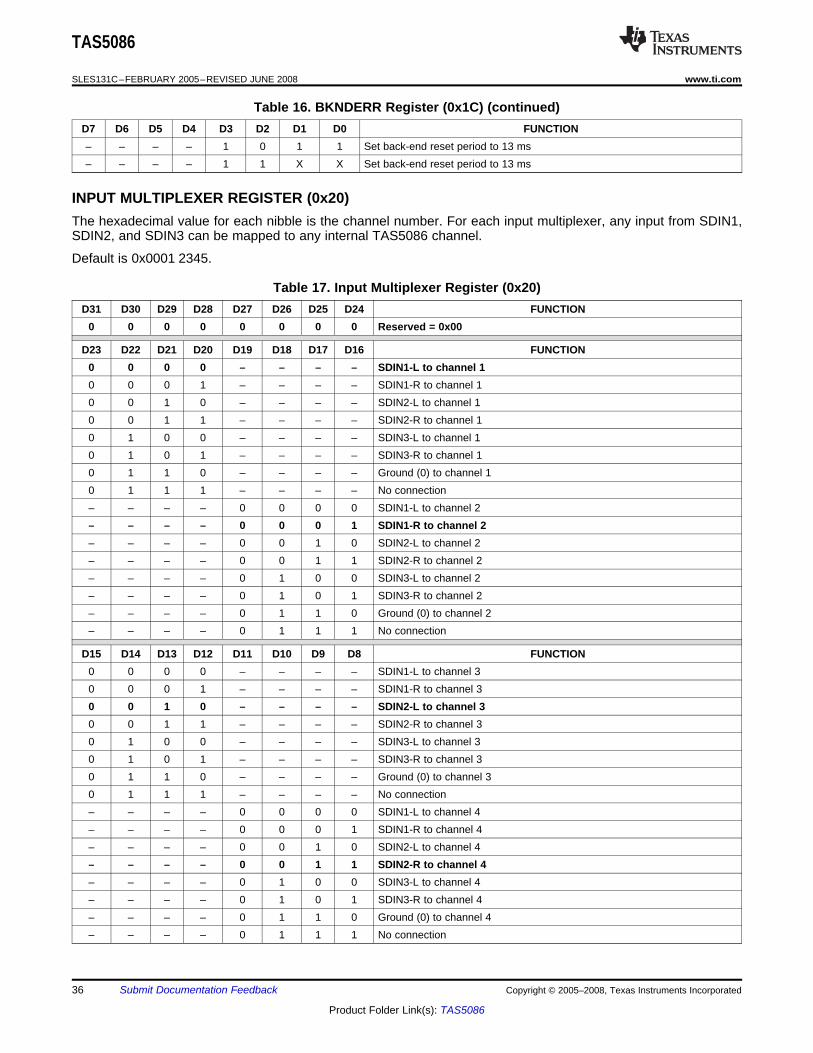
INPUT MULTIPLEXER REGISTER (0x20)
TAS5086
SLES131C–FEBRUARY 2005–REVISED JUNE 2008 ................................................................................................................................................... www.ti.com
Table 16. BKNDERR Register (0x1C) (continued)D7 D6 D5 D4 D3 D2 D1 D0 FUNCTION– – – – 1 0 1 1 Set back-end reset period to 13 ms– – – – 1 1 X X Set back-end reset period to 13 ms
The hexadecimal value for each nibble is the channel number. For each input multiplexer, any input from SDIN1,SDIN2, and SDIN3 can be mapped to any internal TAS5086 channel.
Default is 0x0001 2345.
Table 17. Input Multiplexer Register (0x20)D31 D30 D29 D28 D27 D26 D25 D24 FUNCTION
0 0 0 0 0 0 0 0 Reserved = 0x00
D23 D22 D21 D20 D19 D18 D17 D16 FUNCTION0 0 0 0 – – – – SDIN1-L to channel 10 0 0 1 – – – – SDIN1-R to channel 10 0 1 0 – – – – SDIN2-L to channel 10 0 1 1 – – – – SDIN2-R to channel 10 1 0 0 – – – – SDIN3-L to channel 10 1 0 1 – – – – SDIN3-R to channel 10 1 1 0 – – – – Ground (0) to channel 10 1 1 1 – – – – No connection– – – – 0 0 0 0 SDIN1-L to channel 2– – – – 0 0 0 1 SDIN1-R to channel 2– – – – 0 0 1 0 SDIN2-L to channel 2– – – – 0 0 1 1 SDIN2-R to channel 2– – – – 0 1 0 0 SDIN3-L to channel 2– – – – 0 1 0 1 SDIN3-R to channel 2– – – – 0 1 1 0 Ground (0) to channel 2– – – – 0 1 1 1 No connection
D15 D14 D13 D12 D11 D10 D9 D8 FUNCTION0 0 0 0 – – – – SDIN1-L to channel 30 0 0 1 – – – – SDIN1-R to channel 30 0 1 0 – – – – SDIN2-L to channel 30 0 1 1 – – – – SDIN2-R to channel 30 1 0 0 – – – – SDIN3-L to channel 30 1 0 1 – – – – SDIN3-R to channel 30 1 1 0 – – – – Ground (0) to channel 30 1 1 1 – – – – No connection– – – – 0 0 0 0 SDIN1-L to channel 4– – – – 0 0 0 1 SDIN1-R to channel 4– – – – 0 0 1 0 SDIN2-L to channel 4– – – – 0 0 1 1 SDIN2-R to channel 4– – – – 0 1 0 0 SDIN3-L to channel 4– – – – 0 1 0 1 SDIN3-R to channel 4– – – – 0 1 1 0 Ground (0) to channel 4– – – – 0 1 1 1 No connection
36 Submit Documentation Feedback Copyright © 2005–2008, Texas Instruments Incorporated
Product Folder Link(s): TAS5086

TAS5086
www.ti.com ................................................................................................................................................... SLES131C–FEBRUARY 2005–REVISED JUNE 2008
Table 17. Input Multiplexer Register (0x20) (continued)D7 D6 D5 D4 D3 D2 D1 D0 FUNCTION0 0 0 0 – – – SDIN1-L to channel 50 0 0 1 – – – – SDIN1-R to channel 50 0 1 0 – – – SDIN2-L to channel 50 0 1 1 – – – SDIN2-R to channel 50 1 0 0 – – – SDIN3-L to channel 50 1 0 1 – – – – SDIN3-R to channel 50 1 1 0 – – – – Ground (0) to channel 50 1 1 1 – – – – No connection– – – – 0 0 0 0 SDIN1-L to channel 6– – – – 0 0 0 1 SDIN1-R to channel 6– – – – 0 0 1 0 SDIN2-L to channel 6– – – – 0 0 1 1 SDIN2-R to channel 6– – – – 0 1 0 0 SDIN3-L to channel 6– – – – 0 1 0 1 SDIN3-R to channel 6– – – – 0 1 1 0 Ground (0) to channel 6– – – – 0 1 1 1 No connection
Copyright © 2005–2008, Texas Instruments Incorporated Submit Documentation Feedback 37
Product Folder Link(s): TAS5086

DOWNMIX INPUT MULTIPLEXER REGISTER (0x21)
TAS5086
SLES131C–FEBRUARY 2005–REVISED JUNE 2008 ................................................................................................................................................... www.ti.com
Bits D31–D16: UnusedBits D15–D13: For this description, see Figure 6.
Bit D12: If 1, selects downmix data L’ to TAS5086 internal channel 1If 0, selects channel 1 data (from input multiplexer 1) to the TAS5086 internal channel 1
Bit D11: If 1, selects downmix data R’ to the TAS5086 internal channel 2If 0, selects channel 2 data (from input multiplexer 2) to the TAS5086 internal channel 2
Bit D10: If 1, selects downmix data (L’+R’)/2 to the TAS5086 internal channel 5If 0, selects channel 5 data (from input multiplexer 5) to the TAS5086 internal channel 5
Bits D9-D8: Selects either channel 6 data (from input multiplexer 6) or channel 6 data that has beenprocessed through bass management block or downmix data (L’+R’)/2 to the TAS5086 internalchannel 6
Bits D7–D5: Unused.Bit D4: If 1, enable data from input multiplexer 5 to downmix block
If 0, disable data from input multiplexer 5 to downmix blockBit D3: If 1, enable data from input multiplexer 4 to downmix block
If 0, disable data from input multiplexer 4 to downmix blockBit D2: If 1, enable data from input multiplexer 3 to downmix block
If 0, disable data from input multiplexer 3 to downmix blockBit D1: If 1, enable data from input multiplexer 2 to downmix block
If 0, disable data from input multiplexer 2 to downmix blockBit D0: If 1, enable data from input multiplexer 1 to downmix block
If 0, disable data from input multiplexer 1 to downmix block
Table 18. Downmix Input Multiplexer RegisterD31 D30 D29 D28 D27 D26 D25 D24 FUNCTION
– – – – – – – – Unused
D23 D22 D21 D20 D19 D18 D17 D16 FUNCTION– – – – – – – – Unused
D15 D14 D13 D12 D11 D10 D9 D8 FUNCTION0 1 0 – – – – – RESERVED– – – 1 – – – – Enable downmix data L’ to channel 1– – – 0 – – – – Enable channel 1 data to channel 1– – – – 1 – – – Enable downmix data R’ to channel 2– – – – 0 – – – Enable channel 2 data to channel 2– – – – – 1 – – Enable downmix data (L’+R’)/2 to channel 5– – – – – 0 – – Enable channel 5 data to channel 5– – – – – – 0 0 Enable channel 6 data to channel 6– – – – – – 0 1 Bass management on channel 6– – – – – – 1 x Enable downmix data (L’+R’)/2 to channel 6
38 Submit Documentation Feedback Copyright © 2005–2008, Texas Instruments Incorporated
Product Folder Link(s): TAS5086

AM Mode REGISTER (0x22)
TAS5086
www.ti.com ................................................................................................................................................... SLES131C–FEBRUARY 2005–REVISED JUNE 2008
Table 18. Downmix Input Multiplexer Register (continued)D7 D6 D5 D4 D3 D2 D1 D0 FUNCTION– – – – – – – 1 Enable data from input multiplexer 1 to downmix block– – – – – – – 0 Disable data from input multiplexer 1 to downmix block– – – – – – 1 – Enable data from input multiplexer 2 to downmix block– – – – – – 0 – Disable data from input multiplexer 2 to downmix block– – – – – 1 – – Enable data from input multiplexer 3 to downmix block– – – – – 0 – – Disable data from input multiplexer 3 to downmix block– – – – 1 – – – Enable data from input multiplexer 4 to downmix block– – – – 0 – – – Disable data from input multiplexer 4 to downmix block– – – 1 – – – – Enable data from input multiplexer 5 to downmix block– – – 0 – – – – Disable data from input multiplexer 5 to downmix block
See the PurePath Digital™ AM Interference Avoidance application report (SLEA040).
Table 19. AM Mode Register (0x22)D20 D19 D18 D17 D16 FUNCTION
0 – – – – AM mode disabled1 – – – – AM mode enabled– 0 0 – – Select sequence 1– 0 1 – – Select sequence 2– 1 0 – – Select sequence 3– 1 1 – – Select sequence 4– – – 0 – IF frequency = 455 kHz– – – 1 – IF frequency = 262.5 kHz– – – – 0 Use BCD tuned frequency– – – – 1 Use binary tuned frequency
Table 20. AM Tuned Frequency Register in BCD ModeD15 D14 D13 D12 D11 D10 D9 D8 FUNCTION
0 0 0 X – – – – BCD frequency (1000s kHz)– – – – – – – –– – – – X X X X BCD frequency (100s kHz)0 0 0 0 0 0 0 0 Default value
D7 D6 D5 D4 D3 D2 D1 D0 FUNCTIONX X X X – – – – BCD frequency (10s kHz)– – – – – – – –– – – – X X X X BCD frequency (1s kHz)0 0 0 0 0 0 0 0 Default value
OR
Copyright © 2005–2008, Texas Instruments Incorporated Submit Documentation Feedback 39
Product Folder Link(s): TAS5086

PWM OUTPUT MUX REGISTER (0x25)
TAS5086
SLES131C–FEBRUARY 2005–REVISED JUNE 2008 ................................................................................................................................................... www.ti.com
Table 21. AM Tuned Frequency Register in Binary ModeD15 D14 D13 D12 D11 D10 D9 D8 FUNCTION
0 0 0 0 0 X X X Binary frequency– – – – – – – –0 0 0 0 0 0 0 0 Default value
D7 D6 D5 D4 D3 D2 D1 D0 FUNCTIONX X X X X X X X Binary frequency– – – – – – – –0 0 0 0 0 0 0 0 Default value
This TAS5086 output multiplexer selects which internal PWM channel is output to which pin. Any channel can beoutput to any pin. The default values are used in systems with the TAS5186.
Bits D31–D25: Reserved = 0x00Bits D23–D20: Select which PWM channel is output to PWM_1 (pin 38)Bits D19–D16: Select which PWM channel is output to PWM_2 (pin 37)Bits D15–D12: Select which PWM channel is output to PWM_3 (pin 36)Bits D11–D08: Select which PWM channel is output to PWM_4 (pin 35)Bits D07–D04: Select which PWM channel is output to PWM_5 (pin 34)Bits D03–D00: Select which PWM channel is output to PWM_6 (pin 33)
Note that channels are encoded so that channel 1 = 0x00, channel 2 = 0x01, …, channel 6 = 0x05.
40 Submit Documentation Feedback Copyright © 2005–2008, Texas Instruments Incorporated
Product Folder Link(s): TAS5086

TAS5086
www.ti.com ................................................................................................................................................... SLES131C–FEBRUARY 2005–REVISED JUNE 2008
Table 22. PWM Output Multiplex Register (0x25)D31 D30 D29 D28 D27 D26 D25 D24 FUNCTION
0 0 0 0 0 0 0 0 Reserved = 0x00
D23 D22 D21 D20 D19 D18 D17 D16 FUNCTION0 0 0 0 – – – – Multiplex channel 1 to PWM_1 (pin 38)0 0 0 1 – – – – Multiplex channel 2 to PWM_1 (pin 38)0 0 1 0 – – – – Multiplex channel 3 to PWM_1 (pin 38)0 0 1 1 – – – – Multiplex channel 4 to PWM_1 (pin 38)0 1 0 0 – – – – Multiplex channel 5 to PWM_1 (pin 38)0 1 0 1 – – – – Multiplex channel 6 to PWM_1 (pin 38)– – – – 0 0 0 0 Multiplex channel 1 to PWM_2 (pin 37)– – – – 0 0 0 1 Multiplex channel 2 to PWM_2 (pin 37)– – – – 0 0 1 0 Multiplex channel 3 to PWM_2 (pin 37)– – – – 0 0 1 1 Multiplex channel 4 to PWM_2 (pin 37)– – – – 0 1 0 0 Multiplex channel 5 to PWM_2 (pin 37)– – – – 0 1 0 1 Multiplex channel 6 to PWM_2 (pin 37)
D15 D14 D13 D12 D11 D10 D9 D8 FUNCTION0 0 0 0 – – – – Multiplex channel 1 to PWM_3 (pin 36)0 0 0 1 – – – – Multiplex channel 2 to PWM_3 (pin 36)0 0 1 0 – – – – Multiplex channel 3 to PWM_3 (pin 36)0 0 1 1 – – – – Multiplex channel 4 to PWM_3 (pin 36)0 1 0 0 – – – – Multiplex channel 5 to PWM_3 (pin 36)0 1 0 1 – – – – Multiplex channel 6 to PWM_3 (pin 36)– – – – 0 0 0 0 Multiplex channel 1 to PWM_4 (pin 35)– – – – 0 0 0 1 Multiplex channel 2 to PWM_4 (pin 35)– – – – 0 0 1 0 Multiplex channel 3 to PWM_4 (pin 35)– – – – 0 0 1 1 Multiplex channel 4 to PWM_4 (pin 35)– – – – 0 1 0 0 Multiplex channel 5 to PWM_4 (pin 35)– – – – 0 1 0 1 Multiplex channel 6 to PWM_4 (pin 35)
D7 D6 D5 D4 D3 D2 D1 D0 FUNCTION0 0 0 0 – – – Multiplex channel 1 to PWM_5 (pin 34)0 0 0 1 – – – – Multiplex channel 2 to PWM_5 (pin 34)0 0 1 0 – – – Multiplex channel 3 to PWM_5 (pin 34)0 0 1 1 – – – Multiplex channel 4 to PWM_5 (pin 34)0 1 0 0 – – – Multiplex channel 5 to PWM_5 (pin 34)0 1 0 1 – – – – Multiplex channel 6 to PWM_5 (pin 34)– – – – 0 0 0 0 Multiplex channel 1 to PWM_6 (pin 33)– – – – 0 0 0 1 Multiplex channel 2 to PWM_6 (pin 33)– – – – 0 0 1 0 Multiplex channel 3 to PWM_6 (pin 33)– – – – 0 0 1 1 Multiplex channel 4 to PWM_6 (pin 33)– – – – 0 1 0 0 Multiplex channel 5 to PWM_6 (pin 33)– – – – 0 1 0 1 Multiplex channel 6 to PWM_6 (pin 33)
Copyright © 2005–2008, Texas Instruments Incorporated Submit Documentation Feedback 41
Product Folder Link(s): TAS5086

APPENDIX A. TAS5086 APPLICATIONS
TAS5086
SLES131C–FEBRUARY 2005–REVISED JUNE 2008 ................................................................................................................................................... www.ti.com
For detailed application information, see the TAS5086-5186V6EVM application report (SLEA054).
42 Submit Documentation Feedback Copyright © 2005–2008, Texas Instruments Incorporated
Product Folder Link(s): TAS5086

PACKAGE OPTION ADDENDUM
www.ti.com 15-Apr-2017
Addendum-Page 1
PACKAGING INFORMATION
Orderable Device Status(1)
Package Type PackageDrawing
Pins PackageQty
Eco Plan(2)
Lead/Ball Finish(6)
MSL Peak Temp(3)
Op Temp (°C) Device Marking(4/5)
Samples
SN200608044 ACTIVE TSSOP DBT 38 2000 Green (RoHS& no Sb/Br)
CU NIPDAU Level-2-260C-1 YEAR 0 to 70 TAS5086 B
TAS5086DBT ACTIVE TSSOP DBT 38 50 Green (RoHS& no Sb/Br)
CU NIPDAU Level-2-260C-1 YEAR 0 to 70 TAS5086 B
TAS5086DBTG4 ACTIVE TSSOP DBT 38 50 Green (RoHS& no Sb/Br)
CU NIPDAU Level-2-260C-1 YEAR 0 to 70 TAS5086 B
TAS5086DBTR ACTIVE TSSOP DBT 38 2000 Green (RoHS& no Sb/Br)
CU NIPDAU Level-2-260C-1 YEAR 0 to 70 TAS5086 B
(1) The marketing status values are defined as follows:ACTIVE: Product device recommended for new designs.LIFEBUY: TI has announced that the device will be discontinued, and a lifetime-buy period is in effect.NRND: Not recommended for new designs. Device is in production to support existing customers, but TI does not recommend using this part in a new design.PREVIEW: Device has been announced but is not in production. Samples may or may not be available.OBSOLETE: TI has discontinued the production of the device.
(2) Eco Plan - The planned eco-friendly classification: Pb-Free (RoHS), Pb-Free (RoHS Exempt), or Green (RoHS & no Sb/Br) - please check http://www.ti.com/productcontent for the latest availabilityinformation and additional product content details.TBD: The Pb-Free/Green conversion plan has not been defined.Pb-Free (RoHS): TI's terms "Lead-Free" or "Pb-Free" mean semiconductor products that are compatible with the current RoHS requirements for all 6 substances, including the requirement thatlead not exceed 0.1% by weight in homogeneous materials. Where designed to be soldered at high temperatures, TI Pb-Free products are suitable for use in specified lead-free processes.Pb-Free (RoHS Exempt): This component has a RoHS exemption for either 1) lead-based flip-chip solder bumps used between the die and package, or 2) lead-based die adhesive used betweenthe die and leadframe. The component is otherwise considered Pb-Free (RoHS compatible) as defined above.Green (RoHS & no Sb/Br): TI defines "Green" to mean Pb-Free (RoHS compatible), and free of Bromine (Br) and Antimony (Sb) based flame retardants (Br or Sb do not exceed 0.1% by weightin homogeneous material)
(3) MSL, Peak Temp. - The Moisture Sensitivity Level rating according to the JEDEC industry standard classifications, and peak solder temperature.
(4) There may be additional marking, which relates to the logo, the lot trace code information, or the environmental category on the device.
(5) Multiple Device Markings will be inside parentheses. Only one Device Marking contained in parentheses and separated by a "~" will appear on a device. If a line is indented then it is a continuationof the previous line and the two combined represent the entire Device Marking for that device.
(6) Lead/Ball Finish - Orderable Devices may have multiple material finish options. Finish options are separated by a vertical ruled line. Lead/Ball Finish values may wrap to two lines if the finishvalue exceeds the maximum column width.

PACKAGE OPTION ADDENDUM
www.ti.com 15-Apr-2017
Addendum-Page 2
Important Information and Disclaimer:The information provided on this page represents TI's knowledge and belief as of the date that it is provided. TI bases its knowledge and belief on informationprovided by third parties, and makes no representation or warranty as to the accuracy of such information. Efforts are underway to better integrate information from third parties. TI has taken andcontinues to take reasonable steps to provide representative and accurate information but may not have conducted destructive testing or chemical analysis on incoming materials and chemicals.TI and TI suppliers consider certain information to be proprietary, and thus CAS numbers and other limited information may not be available for release.
In no event shall TI's liability arising out of such information exceed the total purchase price of the TI part(s) at issue in this document sold by TI to Customer on an annual basis.

TAPE AND REEL INFORMATION
*All dimensions are nominal
Device PackageType
PackageDrawing
Pins SPQ ReelDiameter
(mm)
ReelWidth
W1 (mm)
A0(mm)
B0(mm)
K0(mm)
P1(mm)
W(mm)
Pin1Quadrant
TAS5086DBTR TSSOP DBT 38 2000 330.0 16.4 6.9 10.2 1.8 12.0 16.0 Q1
PACKAGE MATERIALS INFORMATION
www.ti.com 14-Jul-2012
Pack Materials-Page 1

*All dimensions are nominal
Device Package Type Package Drawing Pins SPQ Length (mm) Width (mm) Height (mm)
TAS5086DBTR TSSOP DBT 38 2000 367.0 367.0 38.0
PACKAGE MATERIALS INFORMATION
www.ti.com 14-Jul-2012
Pack Materials-Page 2


IMPORTANT NOTICE
Texas Instruments Incorporated (TI) reserves the right to make corrections, enhancements, improvements and other changes to itssemiconductor products and services per JESD46, latest issue, and to discontinue any product or service per JESD48, latest issue. Buyersshould obtain the latest relevant information before placing orders and should verify that such information is current and complete.TI’s published terms of sale for semiconductor products (http://www.ti.com/sc/docs/stdterms.htm) apply to the sale of packaged integratedcircuit products that TI has qualified and released to market. Additional terms may apply to the use or sale of other types of TI products andservices.Reproduction of significant portions of TI information in TI data sheets is permissible only if reproduction is without alteration and isaccompanied by all associated warranties, conditions, limitations, and notices. TI is not responsible or liable for such reproduceddocumentation. Information of third parties may be subject to additional restrictions. Resale of TI products or services with statementsdifferent from or beyond the parameters stated by TI for that product or service voids all express and any implied warranties for theassociated TI product or service and is an unfair and deceptive business practice. TI is not responsible or liable for any such statements.Buyers and others who are developing systems that incorporate TI products (collectively, “Designers”) understand and agree that Designersremain responsible for using their independent analysis, evaluation and judgment in designing their applications and that Designers havefull and exclusive responsibility to assure the safety of Designers' applications and compliance of their applications (and of all TI productsused in or for Designers’ applications) with all applicable regulations, laws and other applicable requirements. Designer represents that, withrespect to their applications, Designer has all the necessary expertise to create and implement safeguards that (1) anticipate dangerousconsequences of failures, (2) monitor failures and their consequences, and (3) lessen the likelihood of failures that might cause harm andtake appropriate actions. Designer agrees that prior to using or distributing any applications that include TI products, Designer willthoroughly test such applications and the functionality of such TI products as used in such applications.TI’s provision of technical, application or other design advice, quality characterization, reliability data or other services or information,including, but not limited to, reference designs and materials relating to evaluation modules, (collectively, “TI Resources”) are intended toassist designers who are developing applications that incorporate TI products; by downloading, accessing or using TI Resources in anyway, Designer (individually or, if Designer is acting on behalf of a company, Designer’s company) agrees to use any particular TI Resourcesolely for this purpose and subject to the terms of this Notice.TI’s provision of TI Resources does not expand or otherwise alter TI’s applicable published warranties or warranty disclaimers for TIproducts, and no additional obligations or liabilities arise from TI providing such TI Resources. TI reserves the right to make corrections,enhancements, improvements and other changes to its TI Resources. TI has not conducted any testing other than that specificallydescribed in the published documentation for a particular TI Resource.Designer is authorized to use, copy and modify any individual TI Resource only in connection with the development of applications thatinclude the TI product(s) identified in such TI Resource. NO OTHER LICENSE, EXPRESS OR IMPLIED, BY ESTOPPEL OR OTHERWISETO ANY OTHER TI INTELLECTUAL PROPERTY RIGHT, AND NO LICENSE TO ANY TECHNOLOGY OR INTELLECTUAL PROPERTYRIGHT OF TI OR ANY THIRD PARTY IS GRANTED HEREIN, including but not limited to any patent right, copyright, mask work right, orother intellectual property right relating to any combination, machine, or process in which TI products or services are used. Informationregarding or referencing third-party products or services does not constitute a license to use such products or services, or a warranty orendorsement thereof. Use of TI Resources may require a license from a third party under the patents or other intellectual property of thethird party, or a license from TI under the patents or other intellectual property of TI.TI RESOURCES ARE PROVIDED “AS IS” AND WITH ALL FAULTS. TI DISCLAIMS ALL OTHER WARRANTIES ORREPRESENTATIONS, EXPRESS OR IMPLIED, REGARDING RESOURCES OR USE THEREOF, INCLUDING BUT NOT LIMITED TOACCURACY OR COMPLETENESS, TITLE, ANY EPIDEMIC FAILURE WARRANTY AND ANY IMPLIED WARRANTIES OFMERCHANTABILITY, FITNESS FOR A PARTICULAR PURPOSE, AND NON-INFRINGEMENT OF ANY THIRD PARTY INTELLECTUALPROPERTY RIGHTS. TI SHALL NOT BE LIABLE FOR AND SHALL NOT DEFEND OR INDEMNIFY DESIGNER AGAINST ANY CLAIM,INCLUDING BUT NOT LIMITED TO ANY INFRINGEMENT CLAIM THAT RELATES TO OR IS BASED ON ANY COMBINATION OFPRODUCTS EVEN IF DESCRIBED IN TI RESOURCES OR OTHERWISE. IN NO EVENT SHALL TI BE LIABLE FOR ANY ACTUAL,DIRECT, SPECIAL, COLLATERAL, INDIRECT, PUNITIVE, INCIDENTAL, CONSEQUENTIAL OR EXEMPLARY DAMAGES INCONNECTION WITH OR ARISING OUT OF TI RESOURCES OR USE THEREOF, AND REGARDLESS OF WHETHER TI HAS BEENADVISED OF THE POSSIBILITY OF SUCH DAMAGES.Unless TI has explicitly designated an individual product as meeting the requirements of a particular industry standard (e.g., ISO/TS 16949and ISO 26262), TI is not responsible for any failure to meet such industry standard requirements.Where TI specifically promotes products as facilitating functional safety or as compliant with industry functional safety standards, suchproducts are intended to help enable customers to design and create their own applications that meet applicable functional safety standardsand requirements. Using products in an application does not by itself establish any safety features in the application. Designers mustensure compliance with safety-related requirements and standards applicable to their applications. Designer may not use any TI products inlife-critical medical equipment unless authorized officers of the parties have executed a special contract specifically governing such use.Life-critical medical equipment is medical equipment where failure of such equipment would cause serious bodily injury or death (e.g., lifesupport, pacemakers, defibrillators, heart pumps, neurostimulators, and implantables). Such equipment includes, without limitation, allmedical devices identified by the U.S. Food and Drug Administration as Class III devices and equivalent classifications outside the U.S.TI may expressly designate certain products as completing a particular qualification (e.g., Q100, Military Grade, or Enhanced Product).Designers agree that it has the necessary expertise to select the product with the appropriate qualification designation for their applicationsand that proper product selection is at Designers’ own risk. Designers are solely responsible for compliance with all legal and regulatoryrequirements in connection with such selection.Designer will fully indemnify TI and its representatives against any damages, costs, losses, and/or liabilities arising out of Designer’s non-compliance with the terms and provisions of this Notice.
Mailing Address: Texas Instruments, Post Office Box 655303, Dallas, Texas 75265Copyright © 2017, Texas Instruments Incorporated