progress on euv industrialization twinscan - asml holding nv
TRANSCRIPT

ASML’s customer magazine | 2012 Issue 1
Progress on EUV Industrialization
TWINSCAN NXT: A thoroughbred workhorse
A bright future for ASML’s refurbished tools

2
images | Colofon
Editorial Board
Lucas van Grinsven, Peter Jenkins
Managing Editor
Ryan Young
Contributing Writers
Rudy Peeters, Stuart Young, Ton van Niftrik,
Jan-Evert van de Wetering, Robert Kazinczi,
Rob van Keulen, Steven van Heek
Circulation
Emily Leung, Michael Pullen, Shirley Wijtman
For more information, please see:
www.asml.com/images
© 2012, ASML Holding BV
ASML, ASM Lithography, TWINSCAN, PAS 5500,
PAS 5000, SA 5200, ATHENA, QUASAR, IRIS, ILIAS,
FOCAL, Micralign, Micrascan, 3DAlign, 2DStitching,
3DMetrology, Brion Technologies, LithoServer,
LithoGuide, Scattering Bars, LithoCruiser, Tachyon
2.0, Tachyon RDI, Tachyon LMC, Tachyon OPC+,
LithoCool, AGILE, ImageTuner, EFESE, Feature Scan,
T-ReCS and the ASML logo are trademarks of ASML
Holding N.V. or of affiliate companies. The trademarks
may be used either alone or in combination with
a further product designation. Starlith, AERIAL,
and AERIAL II are trademarks of Carl Zeiss. TEL is
a trademark of Tokyo Electron Limited. Sun, Sun
Microsystems, the Sun Logo, iForce, Solaris, and the
Java logo are trademarks or registered trademarks of
Sun Microsystems, Inc. in the United States and other
countries. Bayon is a trademark of Kureha Chemical
Industry Co. Ltd. Nothing in this publication is intended
to make representations with regard to whether any
trademark is registered or to suggest that any sign
other than those mentioned should not be considered
to be a trademark of ASML or of any third party.
ASML lithography systems are Class 1 laser products.
6 10 163 Editor’s note
4 Product development with
EUV starts rolling
6 Tomorrow’s CDU performance
at today’s metrology effort
10 Always top performance
at full productivity
16 TWINSCAN NXT
a thoroughbred workhorse
20 A bright future for ASML’s
refurbished tools

3
ASML Images, 2012 Issue 1
Editor’s note
The headlines from SPIE Advanced
Lithography focused on the current
industrialization of EUV, overshadowing
the exciting and equally impressive
results in immersion lithography and
computational lithography. ASML sees
equally important roles for all of these
technologies in the coming years and
presented on all three technology streams.
ASML is working both to industrialize
EUV, and to extend the capabilities of
Immersion, as most of our customers are
planning parallel process developments.
In both cases the proven advantages
of Holistic Lithography provide more
comprehensive customer value in the
effort to perpetuate Moore’s Law.
Let’s start with EUV. The number of
papers, panels and presentations at SPIE
AL demonstrate that the industrialization
of EUV is in full swing. All six of ASML’s
NXE:3100 systems are now installed
at customer sites, are imaging wafers,
and cycles of EUV process learning
are accelerating. The first NXE:3300 is
assembled in Veldhoven and NXE:3300
shipments will begin later this year.
Our expectation is that EUV adoption into
manufacturing will be gradual, and that
EUV and immersion will cohabitate for a
period. Because of this, we are continuing
with innovation on our immersion platform
concurrent with the development of the
EUV platform itself.
The NXT:1950i is the industry workhorse
for leading-edge litho. More than 120
systems have been shipped to memory,
logic and foundry customers, and
throughput numbers above 4,100 wafers
per day have been achieved. To drive
the performance of this system even
further, upgrades in imaging, overlay
and productivity are all underway.
On the Holistic Litho front, new products are
being added. BaseLiner version 1.5 will be
released later this year providing scanner
overlay-related rework reduced by half and
matched-machine overlay improvements
of around 40%. CDU Optimizer improves
on-product CDU performance by over 30%
and implements higher-resolution dose
corrections and CD metrology without
increasing metrology cost. And, Tachyon
FMO (Flexible Mask Optimization) enables
the seamless use of multiple Optical
Proximity Correction (OPC) techniques in
a single mask tapeout, permitting the use
of advanced and computationally intensive
OPC in those local areas where they provide
maximum benefit.
As you may have seen at SPIE AL and as
you will read in this edition of Images,
ASML is working to provide a complete
product portfolio to meet the needs of our
customers, and do so while providing the
highest value.
Regards,
Ryan Young
Multiple and Complimentary Litho StreamsBy Ryan Young, Senior Manager Communications
4
240-nm depth of focus (DoF) and
exposure latitudes of 18% for dense
lines or 14% for isolated lines.
Moreover, using the NXE:3100’s off-axis
illumination capability, customers have
achieved a resolution of 16 nm with
a conventional chemically amplified
photoresist. Importantly, several suppliers
are now offering photoresists capable
of sub-18-nm imaging, which supports
our roadmap for future NXE generations.
However, so far sub-18-nm images have
only been exposed with doses above 30
mJ/cm2, and further work is required to
improve resist sensitivity to 15 mJ/cm2.
Of course, real devices aren’t made of
just line/space patterns. And a particular
advantage of EUV lithography is the
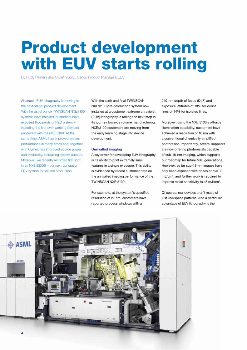
Product development with EUV starts rollingBy Rudy Peeters and Stuart Young, Senior Product Managers EUV
With the sixth and final TWINSCAN
NXE:3100 pre-production system now
installed at a customer, extreme ultraviolet
(EUV) lithography is taking the next step in
its journey towards volume manufacturing.
NXE:3100 customers are moving from
the early learning stage into device
development.
Unrivalled imaging
A key driver for developing EUV lithography
is its ability to print extremely small
features in a single exposure. This ability
is evidenced by recent customer data on
the unrivalled imaging performance of the
TWINSCAN NXE:3100.
For example, at the system’s specified
resolution of 27 nm, customers have
reported process windows with a
Abstract | EUV lithography is moving to
the next stage: product development.
With the last of our six TWINSCAN NXE:3100
systems now installed, customers have
exposed thousands of R&D wafers –
including the first ever working devices
produced with the NXE:3100. At the
same time, ASML has improved system
performance in many areas and, together
with Cymer, has improved source power
and availability, increasing system outputs.
Moreover, we recently recorded first light
in an NXE:3300B – our next-generation
EUV system for volume production.

5
ASML Images, 2012 Issue 1
possibility of imaging complex 2D patterns
at small feature sizes in a single exposure
without stringent design limitations. Again
customer data shows that this possibility
is a reality on the NXE:3100, with the
system’s imaging performance proven
for all relevant device applications.
Beyond imaging
ASML and its customers have also been
making important progress in other
key areas that are vital for making EUV
production ready. Dedicated chuck overlay
(DCO) below 2 nm (with practically no
difference in performance at the edge and
center of the wafer) has been reported by
multiple customers, albeit at a reduced
scan speed. This is well beyond the
system’s specified DCO of 4 nm, and work
to maintain this performance at full scan
speed is ongoing.
Matched machine overlay between the
NXE:3100 and the TWINSCAN NXT:1950i
has been pushed to 4.5 nm while on-
product overlay below 7 nm has been
achieved. Again, both these numbers are
well within specification. In addition, the
installed NXE:3100s have been exhibiting
good overlay stability over periods of
several months.
As a result of these developments,
customers are seeing the potential the
NXE:3100 offers for product development.
The majority of customers have started
exposing R&D wafers for device
development, and thousands of wafers have
now been exposed on NXE:3100 systems
worldwide. And recently, multiple customers
have created working devices using the
NXE:3100 to expose critical layers.
Source developments
Of course, source performance remains a
critical area of interest for EUV lithography.
Here too there have been recent encouraging
developments. At the end of 2011, ASML
and its source partner Cymer released
a source module upgrade that increased
source power and stability, tripling
the NXE:3100’s wafer output. Another
upgrade was implemented at the start
of 2012, further doubling the wafer output
capability to over 300 wafers per week.
Customers have created
working devices using
the NX:3100
These upgrades represent significant
increases in the number of wafers per
week that NXE:3100 systems can deliver.
However, while these system outputs
support the R&D work required to prepare
for high-volume manufacturing, they are
still below the levels needed for production
itself. Hence ASML and Cymer are
engaged in a concerted and collaborative
effort to accelerate source development.
Roadmap to the future
The TWINSCAN NXE:3100 is a pre-
production tool designed to let customers
learn about EUV lithography and carry out
process and product development in this
emerging technology. While there are still
developments to be made, this is a role
the NXE:3100 is now filling.
ASML’s roadmap to volume manufacturing
with EUV includes a number of generations
of production systems. The first of these
is the TWINSCAN NXE:3300B, an
NA = 0.33 scanner with specified resolution
of 22 nm. System assembly has begun at
our dedicated EUV facility in Veldhoven,
The Netherlands. The first fully assembled
system is now ready for integration
testing and we recently achieved first
light in an NXE:3300B. Coming soon
after the announcement of the first ever
working devices from an NXE:3100, this
development is further evidence of EUV
lithography’s progress.
Flash staggered contact layerBitline pitch = 44 nm (1:1.2)
CH pitch = 74.4 nm
Sub 16 nm node �SRAM Contact Hole
0.038µm2 bit cell-size, �hp 30/32 nm
16nm dense lines 27 nm Gate Layer Flash
Sub 16 nm node �SRAM metal-1
0.038µm2 bit cell-size, hp 30/32 nm
30 nm Brickwall DRAM
X=1.1nm y=0.7nm X=1.0nm y=0.9nm X=0.9nm y=1.0nm
X=1.0nm y=1.4nm X=1.0nm y=2.1nm X=0.7nm y=0.4nm
X=0.7nm y=0.9nm X=1.2nm y=1.3nm X=1.0nm y=1.2nm
System A
System B
System C
NXE: 3100 imaging performance proven for customer use cases
Dedicated chuck overlay (DCO) of <2 nm has be achieved on multiple NXE:3100 systems

6
Tomorrow’s CDU performance at today’s metrology effortBy Ton van Niftrik, Product Manager
The drive for feature shrink necessitates
a similar drive to improve on-product
critical dimension uniformity (CDU)
performance, to maintain yields and
profitability at new technology nodes.
Many factors contribute to your on-
product CDU budget, including the
mask, scanner, track and off-scanner
process steps such as etching.
Today’s lithography systems have the
flexibility to compensate for all these
Abstract | CDU Optimizer is a new system
enhancement product from ASML that
helps you achieve the on-product CDU
performance necessary for upcoming
technology nodes. By using dose correction
recipes to compensate for CDU fingerprints
arising throughout the semiconductor
manufacturing process, it can improve
on-product CDU by more than 30%. It is
designed for easy implementation in the fab,
and allows higher-resolution corrections for
future nodes at today’s metrology effort.
contributions. And ASML offers a range
of system enhancement products to
harness that flexibility, and improve
on-product CDU performance. What’s
more, we have a roadmap in place to
ensure new solutions become available
at the right time for your on-product CDU
performance to meet the requirements
of future technology nodes.
The latest product from this roadmap
is CDU Optimizer. Following on from the
0
1
2
3
4
5
2011 2012 2013 2014 2015 2016 2017 2018
CD
U 3
s (n
m)
Year of Production
DRAMFlashMPU
ITRS CDU roadmap

7
ASML Images, 2012 Issue 1
successful DoseMapper, CDU Optimizer
calculates and applies dose corrections
to compensate for intrafield, interfield
and wafer-to-wafer CDU fingerprints
arising anywhere in the semiconductor
manufacturing process. Compared to
DoseMapper, it offers significant CDU
performance improvements for the
same metrology effort.
More freedom to correct
As with DoseMapper, dose corrections
are calculated from production wafer
metrology data and applied to subsequent
wafers through the scanner’s Unicom XL
and Dosicom actuators. However, CDU
Optimizer offers much more freedom in
controlling these actuators, allowing more
precise corrections to be applied.
Improve on-product CDU
performance by over 30%
For example, CDU Optimizer can control
each of the 56 fingers in the Unicom
module individually to create completely
freeform Unicom profiles. It also relaxes
the Dosicom constraints to permit steeper
dose gradients. These two features
improve intrafield CDU in the slit and scan
directions respectively. CDU Optimizer
also allows a different Unicom profile
to be used for each field on a wafer,
reducing CD variations between fields.
In addition, CDU Optimizer lets you apply
different sets of corrections to different
wafers in the same lot. Such “wafer-level”
corrections can be used to compensate
for wafer-to-wafer variations caused, for
example, by processing wafers in different
chambers of the litho cell’s etcher.
Raw data
DoseMapper
(-/-50% in this improvement simulation
based on data)
slit position [mm] 0 10 20 -10 -20
Slit profile
DoseMapper 6 UNICOM groups
DoseMapper
(-/-60% in this improvement
simulation based on data)
CDU Optimizer UNICOM per field
0.5
0.4
0.3
0.2
0.1
0.0
-0.1
0.2
--0.3
-0.4
Correction based on the fingerprints
of etch chamber 1
Correction basedon the average
fingerprint of etch chamber 1 & 2
Correction based on individual
etch chamber fingerprints
35% 55%
Raw data
CD
U 3
s (n
m)
DoseMapper CDU Optimizer
Etch chamber 1Etch chamber 2
Etch chamber 1
Etch chamber 2
CDU Optimizer makes further CDU improvements over DoseMapper
Unicom per field shows best CD control
FreeForm Unicom shows best CD control

8
Reducing the metrology burden
Moving to new technology nodes and
delivering the CDU improvement that
this requires can have a huge impact on
your metrology burden. This is because
achieving better CDU usually means you
must measure more data points per critical
layer, while smaller feature sizes mean
there are more critical layers in a device.
space (S2) and the difference between
them (S1-S2) in a typical spacer process.
In this case, CDU Optimizer enabled a
30% reduction in the 3σ value for the
variation of S1-S2.
A perfect partnership
CDU Optimizer’s ability to determine
the right dose corrections and hence
improve on-product CDU depends
strongly on the quality of metrology data
available. This makes ASML’s YieldStar
metrology tool the perfect metrology
partner for CDU Optimizer.
YieldStar is extremely fast and precise.
Not only does it demonstrate almost
perfect correlation with CD-SEM results
(the current gold standard in fabs),
it has been shown to be significantly
more precise. This improves the ability to
determine process fingerprint, ultimately
resulting in lower CDU. At the same time,
YieldStar is much faster than CD-SEM,
enabling more measurements to be
performed in a production environment
which in turn allows better capture of
process variations (J. Lee et al, SPIE 2012).
Spacer balancing to enable
future nodes
Future technology nodes will employ an
increasing number of double or multiple
patterning layers. A popular choice for
implementing multiple pattering are the
so-called spacer techniques, where a layer
of spacer material is deposited onto the
patterned wafer and etched away so as
to increase the density of features on the
wafer. This introduces two separate feature
spacing parameters: one governed by the
lithography step and one by the spacer step.
To ensure end-product performance, these
two spaces should be as close to equal
as possible. But because they arise from
separate steps, this “spacer balancing”
can be difficult to achieve. However,
CDU Optimizer allows you to use dose
corrections to co-optimize lithography and
process fingerprints. This reduces both
the average difference between the two
spaces and its variation across the wafer –
improving yields and device performance.
For example, figure X shows the variation
in the lithography space (S1), the spacer
018
19
20
21
22
23
50 100 150 010
11
12
13
14
15
50 100 150 0
8
7
6
5
10
11
50 100 150
No dose correction for S1/S2 applied
3s = 2.7nm
S1 (litho) S2 (process) S1 - S2
3s = 1.8nm 3s = 4.0nm
3s = 2.4nm 3s = 1.3nm 3s = 2.6nm
018
19
20
21
22
23
50 100 150 010
11
12
13
14
15
50 100 150 0
8
9
9
7
6
5
10
11
50 100 150
Dose correction for S1/S2 applied
R2 = 0.88
S1-S2 Scat. (nm)
S1-
S2
SEM
(nm
)
-2 -1 0 1 2-3-4
Correlation plot
YieldStar Scatterometry to CD-SEM
correlation plot
Key metric in Spacer Technology, improved by more than 1nm

9
ASML Images, 2012 Issue 1
To some extent, YieldStar alone can help
alleviate this problem as its speed – less
than a second per measurement rather
than 2-3 seconds for CD-SEM – helps
reduce metrology cost-of-ownership.
However, even with this improved
metrology throughput, the current way
of working will soon lead to an unfeasible
metrology burden for future nodes.
Consequently, CDU Optimizer employs a
novel approach to dose recipe generation
that greatly reduces the amount of
metrology required, allowing manufacturers
to implement higher-resolution dose
corrections and CD metrology at today’s
cost. This approach separates product
fingerprints (arising from the reticle) and
process fingerprints (coming from etch
or bake steps for instance), enabling
redundant measurements to be identified
and eliminated.
To illustrate this, imagine a hypothetical
fab set up where two reticles are used
to produce the same product, and
wafers can be sent to either of two
etch chambers. In the traditional way of
working, the manufacturer would need to
perform intrafield and interfield metrology
on all four combinations. That means
8 sets of measurements are required.
With CDU Optimizer, the manufacturer
only needs to perform intrafield metrology
for each mask and interfield metrology for
each etch chamber – so just 4 sets of
measurements.
Implement higher-
resolution dose corrections
and CD metrology at
today’s cost
In a real foundry use case, this enables
huge metrology time savings of around
95%. For example, in a typical use
case involving 100 reticles and 5 etch
chambers, CDU optimizer could reduce
metrology time from 350 hours to just 17.
At the same time, the number of send-
ahead wafers is reduced from 500 to 104.
Improving fab economics
CDU Optimizer is designed for maximum
flexibility and cost-effectiveness in
implementation. It includes a tool for
optimizing metrology sampling schemes
and determining the most cost-efficient
solution metrology set-up. It also features
an improved graphical user interface and
allows several automation implementation
possibilities in the fab.
CDU Optimizer is a further example of
how ASML helps you address the drive for
feature shrink through a complete product
portfolio that integrates control, metrology
and computational functionality as well
as the scanner. This integrated offering
helps you to improve on-product CDU
performance by over 30% and enables
the transition to future technology nodes
while keeping overall fab yields and
profitability high.
Context DoseMapper CDU Optimizer
Send ahead wafer
Required measurements
Send ahead wafer
Required measurements
Mask 1, Etcher A Yes Yes
Mask 1, Etcher B Yes Yes
Mask 2, Etcher A Yes Yes
Mask 2, Etcher B Yes No
X Redundant measurement, reduction of metrology & send ahead time

10
Always top performance at full productivityBy Jan-Evert van de Wetering, Product Manager

11
ASML Images, 2012 Issue 1
Always top performance at full productivityBy Jan-Evert van de Wetering, Product Manager
Abstract | ASML’s BaseLiner scanner
option ensures stable overlay and focus
performance over long periods of time.
It allows TWINSCAN scanners to operate
within ATP specifications continuously
for a scanner time investment of a few
minutes every three days. With BaseLiner,
you can improve system productivity and
machine overlay matching while reducing
rework to improve your overall output of
good wafers. Moreover, BaseLiner can also
restore fingerprints, helping reduce work
in progress (WIP) qualification time after
machine interventions. BaseLiner turns
engineering time into productive time.

12
Traditional approaches to addressing
drift in volume manufacturing typically
involve re-calibrating the scanner either
after a given period of time or when it
has drifted beyond a pre-defined amount
away from its specified performance.
The frequency between re-calibrations
is a careful economic balance between
reducing yield losses due to drift and
minimizing scanner downtime.
ASML’s BaseLiner scanner option
offers a better way to tackle drift. It
allows TWINSCAN scanners to operate
continually within their ATP specifications
and requires just a few minutes of scanner
time every few days. BaseLiner ensures
overlay and focus stability, improves
scanner matching and increases system
productivity. In short, it turns engineering
time into an increased number of good
The extreme complexity of cutting-
edge lithography systems has made
“drift over time” – the gradual change
in a scanner’s performance over time
- a fact of life. At larger feature sizes,
manufacturing tolerances were bigger
and drift was easily manageable.
However, as features shrink and
tolerances become tighter, the potential
impact drift has on yield has grown.
Customers have
seen scanner
overlay-related
rework halve
Baseliner Server
Baseliner Wafers
Focus and Overlay measurements
YieldStarmetrology
Measure Overlay and FocusFingerprints Periodically
reference current
BaseLiner ‘Loop’ controls overlay and focus to a preferred fingerprint

13
ASML Images, 2012 Issue 1
wafers per month a fab can produce, even
when moving to next node. What’s more,
it significantly reduces the amount of time
engineers spend on re-calibration and
qualification of work in progress (WIP)
after a system intervention, freeing up
valuable man-hours for other tasks.
Speed and simplicity
BaseLiner is a software product that
uses an off-line metrology feedback loop
to keep TWINSCAN scanners performing
to a customer-defined baseline.
That baseline is established by exposing
reference wafers and measuring the
scanner’s overlay and focus fingerprints.
Then, by periodically exposing dedicated
BaseLiner wafers, any variations in
those fingerprints can be monitored
and corrections calculated to return
the scanner to its initial performance.
15.0
17.5
12.5
10.0
7.5
6.0
over
lay
X (n
m)
X overlay Chuck 2
9 nm�
(mean) + 3s/Wafer/Uncontrolled Absolute
(mean) + 3s/Wafer/Controlled Absolute
5.5 nm�
5 months
12
10
8
6
4
2
0
12
10
8
6
4
2
0
(nm) (nm)
1 month
4 nm
Overlay XT:1400F matched to NXT:1950i�(chuck 1, x)
2 nm
Upgrade TOP3�and set BaseLine
BaseLiner applied to XT:1400E improves 5-month overlay stability with a factor 2x
BaseLiner applied to XT:1400F with TOP3 matched to NXT: stable and well below 8 nm without overlay
maintenance time

14
The beauty of BaseLiner is that it allows
these periodic checks and corrections
to be carried out with the minimum of
scanner and engineer time. Fingerprints
can be determined by exposing just four
wafers (two per chuck), and these wafers
are measured in an off-line metrology
tool not the scanner itself. So the scanner
can be back producing wafers in just a
few minutes.
Once exposed, the in-resist focus and
overlay fingerprint for the BaseLiner
wafers can be measured using ASML’s
YieldStar 3-in-1 metrology system.
YieldStar is more precise than other
metrology systems, ensuring robust
BaseLiner performance. It is also
much faster, capable of measuring
four BaseLiner wafers in just two hours
compared to five hours for a typical
metrology tool. This means one YieldStar
system can handle the BaseLiner
metrology for a large number of systems
– and still have plenty of capacity for other
offline metrology tasks. For customers
planning ahead, for on-product focus
metrology and even more sophisticated
overlay improving applications, the
integrated YieldStar T-200 metrology will
smoothly take over, making BaseLiner
operation in HVM even easier.
The measured overlay and focus
fingerprints are fed from the YieldStar
metrology system into BaseLiner’s
calculation engine. This sophisticated
software engine compares the scanner’s
current fingerprints with the reference
fingerprint. In addition, because the
engine includes real scanner models,
it can accurately calculate the exposure
corrections required to return the
scanner’s performance back to the
baseline at the push of a button.
Matched-machine overlay to NXT:1950i of less than
8 nm possible on dry ArF scanners
15.0
12.5
10.0
7.5
nm
2 months
Matched�Overlay
Filtered overlay (99.7%)�NXT:1950i matched to 2DE wafer with BaseLiner
3.5 nm�no BaseLiner
2 nm�with BaseLiner
Focus�Uniformity
40
30
20
10
nm
2 months4 months
< 6 nm
No Baseliner With Baseline
Standard
BaseLiner controlled
Major upgrade
BaseLiner increases NXT long-term overlay stability with more than 1.5 nm
without overlay maintenance time
BaseLiner keeps NXT focus uniformity stable and well below 25 nm
without focus maintenance time
15
ASML Images, 2012 Issue 1
Improves scanner
productivity by
around 1.5%
The corrections are fed back to the
scanner via the fab automation system.
Running on a dedicated BaseLiner
server, the engine performs the whole
comparison and calculation process in
just three minutes – saving hours
of engineering time.
Flexibility in implementation
BaseLiner offers a lot of freedom for
customization in implementation and
delivery. Fingerprint measurements
can be performed at any frequency the
customer chooses, but to ensure target
performance is continuously maintained,
it is recommended that checks are carried
out every three days.
The correction calculation engine
requires a server (one per fab) supported
with a dedicated Lithography Computing
Platform which is easily scalable for
adding further computational lithography
tools or other wafer fab applications.
Delivering real results
Since its launch, BaseLiner has proven
extremely popular with ASML customers.
Almost all customers running TWINSCAN
NXT or latest generation immersion XT
systems opt for the BaseLiner scanner
stability option. And they have been
reporting back some impressive results.
Typically, BaseLiner improves scanner
productivity by around 1.5%. At the
same time, customers have seen
scanner overlay-related rework halve and
matched-machine overlay improvements
of around 40%. And this has been
achieved with a labor saving of multiple
full-time equivalents (FTEs). The end
result is that, when equipping a whole fab
with the BaseLiner-YieldStar combination,
many customers recover their investment
in just 4 months.
BaseLiner also works well on dry ArF tools.
Latest customer data has shown that
XT:1400F matched overlay towards
NXT:1950i can be kept well below 8 nm
and, with additional corrections per
exposure even below 6 nm. Not once,
but every day.
Continuous improvement
BaseLiner is part of ASML’s ongoing effort
to help customers optimize their on-product
performance and increase yields. As
such, ASML has a detailed roadmap
for expanding BaseLiner’s functionality
and extending its applicability beyond
TWINSCAN XT and NXT systems to the
emerging TWINSCAN NXE EUV platform.
At the end of 2011, ASML released a
BaseLiner functionality upgrade called
BaseLiner 1.5. This upgrade improves
matched machine overlay (MMO) right
across the fab by allowing all systems to be
matched to one “golden reference” wafer.
In essence, BaseLiner allows customers
to “copy” their existing golden reference
wafer as many times as they like without
having to invest in scanner time, typically
boosting productivity by a further 0.5%.
Again, most of the work is done in the
offline YieldStar tool.
To make these copies, BaseLiner
calculates the difference between the
golden reference wafer and a standard
BaseLiner wafer exposed on each
scanner. The BaseLiner wafer plus the set
of differences acts as a new copy of the
reference. Every scanner in the fab – from
i-line to EUV – can then be matched to this
golden reference, increasing fab efficiency
significantly. BaseLiner 1.5 makes fleet-
matching easy.
Many customers recover
their investment in just
4 months
High-volume manufacturing at small
feature lengths means optimizing on-
product performance while keeping
the economics under control through
maximum productivity and yield.
By ensuring scanners continuously
operate according to specifications,
BaseLiner reduces both production
stoppages and the amount of reworking
required, so fabs can produce more
good wafers per month.

16
TWINSCAN NXTa thoroughbred workhorseBy Robert Kazinczi, Director Product Management
17
ASML Images, 2012 Issue 1
Abstract | The TWINSCAN NXT:1950i was
first released in 2009, allowing customers
to start learning about this revolutionary
high-throughput, high-precision immersion
ArF system. It has now evolved into a
mature, high-output solution for volume
production at today’s smallest nodes.
In the coming years, the NXT will continue
evolving through platform improvements
and system enhancement packages
to support the industry’s migration to
2x nodes and beyond.
ASML’s TWINSCAN NXT:1950i immersion
ArF scanner was designed to be a
thoroughbred among lithography systems.
Its ambitious specifications aim to make
multiple patterning in the fab feasible –
both technically and economically.
Outputs above 4100
wafers per day
But in the three years since its launch,
the TWINSCAN NXT has evolved from the
“new kid on the block” into mature
solution for high-volume production.
The thoroughbred has become a
workhorse – albeit one that targets
the cutting-edge of semiconductor
manufacturing. What’s more, ASML
has a detailed roadmap in place for
continuing that evolution over the next
three years, enhancing performance
and output to support high-volume
manufacturing down to 1x nodes.
A mature performer
The first TWINSCAN NXT systems were
shipped in 2009, allowing customers to
start learning about the new platform at
an early stage. Since then, ASML has
released a number of upgrades to bring
the platform to a production-ready state.

18
As usual with ASML, the improvements
and options will be available as in-field
upgrades, allowing manufacturers to
re-use their current installed base for
future nodes, maximizing their return on
investment in the NXT and making the
transition to new nodes more affordable.
It will also provide greater flexibility in
managing the switch to extreme ultraviolet
(EUV) lithography by allowing fab refits
to be carried out in line with planned
investment cycles.
Key targets in extending the NXT for 1x
production include squeezing on-product
overlay to just 4 nm and the total focus
budget to 60 nm. The aim is to deliver
these performance improvements while
simultaneously increasing full-field
throughput to 250 wph.
At these incredibly small feature
sizes, defects become an increasingly
challenging issue. So an important part
of preparing the NXT for 1x nodes will be
maintaining or even improving defectivity
performance. Here the main focus is on
reducing so-called “big bubble” defects.
ASML is already developing platform
enhancements that should practically
eliminate big bubbles at full throughput and
significantly improve overall defect levels
beyond the 10 per wafer typical today.
These defectivity upgrades, and others
to support production at 1x nodes, will be
available to customers starting in 2013.
Supporting industry needs
In the three years since its launch, the
TWINSCAN NXT:1950i has become well
established across the industry. During
that time, the system has evolved from
an R&D tool for early learning to a mature
solution for high-volume production.
That evolution is set to continue,
enabling manufacturers to address 2x
and 1x nodes with multiple patterning
immersion ArF lithography and manage
a smooth transition to EUV. Throughout
that evolution, the TWINSCAN NXT will
combine cutting-edge imaging and overlay
with unrivalled throughput and excellent
reliability, making it both a thoroughbred
performer and real fab workhorse.
performance gains at the same or better
imaging, overlay or focus performance.
Indeed, during beta testing, systems
that had been upgraded with the PEP
NXT package performed better than
specification in all key areas including
3-day dedicated chuck overlay, MMO,
CDU, focus uniformity, 3-day focus
stability and defectivity. In particular,
the enhanced system set-up significantly
improved overlay performance towards
the edge of the wafer, enabling an
unfiltered full-wafer MMO of 5.5 nm
at 200 wph.
Increased productivity makes production
at 2x nodes using multiple patterning
strategies financially viable. Such
strategies put greater demand on the
on-product performance a litho cell
can deliver. Hence, over the course of
2012, ASML will be releasing a number
of system enhancement packages to
improve on-product overlay and imaging
Unfiltered full-wafer
MMO of 5.5 nm
at 200 wph
For overlay, options will include TOP
packages, GridAlign next-generation
alignment and an updated Overlay
Optimizer. Imaging options will include
a focus improvement package, BaseLiner
scanner stability (see page 10), CDU
Optimizer (see page 6) and a new version
of the AGILE (air gauge improved process
leveling) system. Together, these
enhancements push matched machine
overlay (MMO) to 4.5nm, on-product
overlay down to 6 nm, CDU to 1.5 nm
and total focus control to 80 nm.
Toward 1x nodes
Looking further ahead, ASML plans to
continue extending the NXT platform
to support production at 1x nodes.
Again, this evolution will be delivered
through a mix of improvements to the
baseline platform and optional system
enhancement packages.
In particular, service pack options
released in the last twelve months have
brought average availability up to 92%
for production systems. They have also
ensured systems consistently perform
according to customers’ expectations
– both under ATP conditions and on-
product. That means throughputs of
175 wafers per hour (wph) under ATP
conditions and 190 wph under full-field
conditions. ATP matched machine
overlay (MMO) is just 5.5 nm and critical
dimension uniformity is 2.5 nm, while
on-product overlay of better than 8 nm
is regularly achieved.
Those numbers have seen the NXT
become a popular choice for fabs in all
sectors of the semiconductor industry.
Some 120 systems have been shipped to
memory, logic and foundry customers, and
are performing according to specification
day in, day out. Outputs above 4100 wafers
per day have been achieved, and individual
NXT systems have already exposed more
than one million wafers.
Ongoing evolution for 2x nodes
The combination of thoroughbred
performance and workhorse production
has seen the TWINSCAN NXT become
well established for volume production
at today’s cutting-edge nodes. However
the NXT was always intended as a
multi-node system, and ASML has a
detailed roadmap to extend the system’s
performance in line with industry demand
for manufacturing at 2x nm nodes.
This roadmap includes both upgrades
to the baseline platform and optional
system enhancement packages.
A number of these planned option
packages – including productivity
upgrades, overlay improvements and
the FlexWave programmable wavefront
solution – were discussed in last
summer’s issue of Images. And the first
of them, the PEP NXT productivity
upgrade, has already started shipping.
The PEP NXT:1950i package increases
system productivity by 15-20%, making
full-field throughput of 230 wph possible.
Importantly, the upgrade enables these

19
ASML Images, 2012 Issue 1
0
2
4
6
8
1 2 3 4
YXLot (1.5,1.3)
Lot 1
wafer wafer wafer
Lot 2 Lot 3
Ove
rlay
(99.
7% ),
nm
Ove
rlay
(99.
7% ),
nm
Ove
rlay
(99.
7% ),
nm
0
2
4
6
8
1 2 3 4
YXLot (1.6,2.0)
0
2
4
6
8
1 2 3 4
YXLot (1.7,2.0)
1.5 nm
4.8 nm
2.0 nm 2.0 nm
Stable 2 nm full wafer overlay exposed at 230 wph dedicated chuck mode
Matched machine overlay improved to sub 5 nm full wafer
0
2.5
5
7.5
10
1 2 3
YXLot (4.6,4.8)
wafer
Ove
rlay
99.7
% u
nfilt
ered
[nm
]
NXT:1950i1H2012
0
1
2
3
4
5
6
NXT:1950i1H2011
Typical matching performance (machine to machine)
< Overlay Grid
NXT:1950i2H2011
7
Ove
rlay
99.7
% u
nfilt
ered
[nm
]
10 nm 99.7%x: 1.5 nmy: 1.3 nm
10 nm 99.7%x: 4.6 nmy: 4.8 nm
10 nm 99.7%x: 1.6 nmy: 2.0 nm
10 nm 99.7%x: 1.7 nmy: 2.0 nm
MMO

20
Linkou

21
ASML Images, 2012 Issue 1
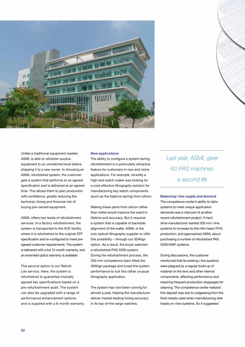
That’s why we established the 200 mm
competence center in 2009. Today, the
competence center comprises some
200 engineers based at the ASML
Center of Excellence (ACE) in Linkou,
Taiwan supported by a similar number
of colleagues in Europe and the US –
all dedicated to our PAS 5500
lithography platform.
Concentrating our smaller-wafer know-
how in this way creates a critical mass of
expertise covering system development,
manufacturing and customer support.
This in turn allows us to continue
offering a complete range of life-cycle
management services for PAS 5500
systems. These include expert service
support, refurbishing and reselling used
systems and developing new products
that improve performance or tailor
systems for new applications.
Second life
The continued importance of the 200
mm and below sector drives a strong
market for pre-owned systems. ASML is
active in this market through the 200 mm
competence center. Last year, ASML gave
some 60 PAS machines a second life
– 30 through direct fab-to-fab shipping
and 30 through refurbishment.
A bright future for ASML’s refurbished toolsBy Rob van Keulen, Director Mature Products & Services, and Steven van Heek, New Business Development & Marketing
Production on 300 mm wafers may now
be the mainstream, but the 200 mm and
smaller sector is still hugely important in
the semiconductor industry. Around 50%
of wafers processed globally are 200 mm
or smaller – accounting for about 25% of
chip production. These smaller wafer sizes
are particularly attractive for special
applications and smaller-volume markets.
Indeed, the sector is predicted to continue
growing over the long term in areas such
as MEMS, analog, LEDs, hard disks and
bio-electronics.
Ongoing commitment
to service and enhance
the installed base
Going back more than 25 years, ASML’s PAS
systems have always led the way in customer
value through a combination of performance
and productivity at wafers sizes ranging from
75 to 200 mm (3”-8”). As a result, the current
PAS installed base comprises some 2000
systems worldwide. And although ASML
no longer manufactures new PAS systems,
we are still committed to ensuring the
installed base delivers maximum value.
Abstract | Based at the ASML Center of
Excellence (ACE) in Linkou, Taiwan, ASML’s
200 mm competence center is a unique
resource for customers of the PAS 5500
platform. It provides a critical mass of
expertise, ensuring valuable knowledge
of this popular platform is retained in the
semiconductor industry. It offers expert
service support, pre-owned systems
refurbished to the highest standards, and
new products that improve performance
or tailor systems for new applications.
22
Unlike a traditional equipment reseller,
ASML is able to refurbish surplus
equipment to an unmatched level before
shipping it to a new owner. In choosing an
ASML refurbished system, the customer
gets a system that performs to an agreed
specification and is delivered at an agreed
time. This allows them to plan production
with confidence, greatly reducing the
technical, timing and financial risk of
buying pre-owned equipment.
ASML offers two levels of refurbishment
services. In a factory refurbishment, the
system is transported to the ACE facility
where it is refurbished to the original ATP
specification and re-configured to meet pre-
agreed customer requirements. The system
is delivered with a full 12 month warranty, and
an extended optics warranty is available.
The second option is our Refurb
Lite service. Here, the system is
refurbished to guarantee mutually
agreed key specifications based on a
pre-refurbishment audit. The system
can also be upgraded with a range of
performance enhancement options,
and is supplied with a 6-month warranty.
New applications
The ability to configure a system during
refurbishment is a particularly attractive
feature for customers in new and niche
applications. For example, recently a
high-end watch maker was looking for
a cost-effective lithography solution for
manufacturing key watch components
(such as the balance spring) from silicon.
Making these parts from silicon rather
than metal would improve the watch’s
lifetime and accuracy. But it requires
a system that is capable of backside
alignment of the wafer. ASML is the
only optical lithography supplier to offer
this possibility – through our 3DAlign
option. As a result, the buyer selected
a refurbished PAS 5500 system.
During the refurbishment process, the
200 mm competence team fitted the
3DAlign package and tuned the system
performance to suit this rather unusual
lithography application.
The system has now been running for
almost a year, helping the manufacturer
deliver market leading timing accuracy
in its top-of-the range watches.
Last year, ASML gave
60 PAS machines
a second life
Balancing i-line supply and demand
The competence center’s ability to tailor
systems to meet unique application
demands was a vital part of another
recent refurbishment project. A hard
drive manufacturer wanted 200 mm i-line
systems to increase its thin-film head (TFH)
production, and approached ASML about
purchasing a number of refurbished PAS
5500/450F systems.
During discussions, the customer
mentioned that its existing i-line systems
were plagued by a regular build up of
material on the lens and other internal
components, affecting performance and
requiring frequent production stoppages for
cleaning. The competence center realized
this deposit was due to outgassing from the
thick resists used when manufacturing disk
heads on i-line systems. So it suggested

23
ASML Images, 2012 Issue 1
systems in the field. Through its service
solutions, it tracks wear and tear on parts.
It also actively engages with the supply
chain to monitor, identify and solve spare
parts supply issues. This information
can help customers plan maintenance
programs, and is also important input for
our refurbishment projects. Moreover, the
competence center solves around 20 End
of Life issues per quarter for customers.
Ongoing commitment
ASML’s 200 mm competence center is a
unique resource for PAS 5500 customers.
By providing a focal point for our smaller-
wafer know-how, it ensures valuable
knowledge about the platform is retained
in the industry for customers to call on.
As a result, customers can be sure of the
best cost and value of ownership whether
they are looking to purchase pre-owned
systems or extend the profitability of their
existing equipment. The center is a sign
of ASML’s ongoing commitment to
service and enhancement of the installed
base for a platform that continues
to play an important role in today’s
semiconductor industry.
a significant undertaking, the PAS 5500’s
modular architecture helps keep delivery
times down. And the conversion means
customers have access to new i-line tools
on a planned timeline.
Systems refurbished
to meet unique application
demands
Extending productive lifetimes
Besides these “second life” services,
the competence center also brings
added value for customers who
already have an installed base of PAS
5500 systems. The center offers a full
range of service solutions, allowing
manufacturers to balance costs while
gaining maximum value. It also provides
extensive application and equipment
support such as productivity and yield
enhancement projects.
In addition, the competence center
helps extend the lifetime of all PAS 5500
adding an extraction hood, which it
designed and then fitted as part of the
refurbishment process. The extraction hood
works so well, it has now been fitted to the
customer’s other i-line tools.
This project also highlighted another way the
200 mm competence center adds value to
the used equipment market: by balancing
supply and demand for different system
types. As the original manufacturer of the
PAS 5500 systems, ASML is uniquely placed
to convert systems from one lithography
wavelength to another. Here the customer
was looking for a PAS 5500/450F. Indeed,
there is strong demand in many markets
for this top-of-the-range i-line system.
But only a very limited number of units
become available on the pre-owned market.
So ASML purchased a surplus PAS
5500/500 KrF system and converted
it to a PAS5500/450 i-line system. This
involves replacing the lens, light source
and associated components, while the
rest of the system underwent a standard
refurbishment plus customized adjustments
to prevent ESD damage to the TFH wafers.
Although conversion from KrF to i-line is

www.asml.com
Corporate Headquarters
De Run 6501
5504 DR Veldhoven
The Netherlands
Phone +31 40 268 30 00
United States
8555 South River Parkway
Tempe, AZ 85284 USA
Phone +1 480 383 4422
Asia
Suite 1702-3 17th Floor
100 Queen’s Road Central
Hong Kong, SAR
Phone +852 2295 1168