programmed data processor-l manual - gordon bellgordonbell.azurewebsites.net/digital/pdp 1 manual...
TRANSCRIPT

PROGRAMMED
DATA PROCESSOR-l
MANUAL
DIGITAL EQUIPMENT CORPORATION
Maynard l Massachusetts

Programmed Data Processor-l
Copyright 1961 by Digital Equipment Corporation

I. INTRODUCTION . . . . . . . . . . . . . . . . . . . . . . . . . . . 4
Central Processor Memory System Input-Output
II. PROGRAMMING PDP-1 . . . . . . . . . . . . . . . . . . 6
Number System Instruction Format Indirect Addressing Operating Speeds Manual Controls Instruction List
Ill. STANDARD AND OPTIONAL EQUIPMENT . . . . . . . . . . . . . . . . . . . .
Standard Equipment Optional Equipment
IV. PROGRAM LIBRARY . . . . . . . . . .
V. APPENDIX . . . . . . . . . . . . . . . . . . . . . .
Abbreviated Instruction List Numerical Instruction List Alphanumeric Codes
. . . .
. . . .
. . . .
. . . . . . . 22
....... 30
....... 32

I. INTRODUCTION
The Programmed Data Processor (PDP-1) is a high speed, solid state digital computer designed to operate with several types of input-output devices, with no internal machine changes. It is a single address, single instruction, stored program computer with powerful program features. Five-megacycle circuits, a magnetic core memory, and fully parallel processing make possible a compu- tation rate of 100,000 additions per second (about 2.5 times the speed of most large computers in use today, and more than 100 times the speed of magnetic drum computers). The PDP-1 is unusually versatile. It is easy to install, operate and maintain. Conventional IlO-volt power is used, neither air conditioning nor floor reinforce- ment is necessary, and preventive maintenance is provided for by built-in marginal checking circuits.
PDP-1 circuits are based on the designs of DEC’s highly success- ful and reliable System Modules. Flip-flops and most switches use saturating transistors. Primary active elements are Micro- Alloy and Micro-Alloy-Diffused transistors.
The entire computer occupies only 17 square feet of floor space. It consists of four equipment frames, one of which is used as the operating station.
CENTRAL PROCESSOR
The Central Processor contains the control, arithmetic and mem- ory addressing elements and the memory buffer register. The word length is 18 binary digits. Instructions are carried out in multiples of the memory cycle time of five microseconds. Add, subtract, deposit, and load, for example, are two-cycle instructions requiring 10 microseconds. Multiplication, by subroutine, requires 325 micro- seconds on the average. Program features include: single address instructions, multiple step indirect addressing and logical arith- metic commands. Console features include: flip-flop indicators grouped for convenient octal reading, six program flags for auto- matic setting and computer sensing and six sense switches for man- ual setting and computer sensing.
MEMORY SYSTEM
The coincident-current, magnetic core memory holds 4096 words of 18 bits each. Up to eight additional memory units of the same capacity may be readily added to the machine; a memory field switch instruction built into PDP-1 will then select the correct memory module. The read-rewrite time of the memory is five microseconds, the basic computer rate. Driving currents are auto- matically adjusted to compensate for temperature variations
4

A Standard DEC System Module used in PDP-1
between 50 and 110 degrees Fahrenheit. The core memory storage may be supplemented by up to 24 magnetic tape transports.
INPUT-OUTPUT PDP-1 is designed to operate a variety of input-output devices.
Standard equipment consists of a punched tape reader with a read speed of 400 lines per second, an alphanumeric typewriter for on-line operation in both input and output and a punched tape punch (alphanumeric or binary) with a speed of 63 lines per second. Optional external equipment includes: compatible mag- netic tape (75 inches per second, BCD or binary); 16-inch cathode ray tube for graphic or tabular displays; light pen input; line printer (150 or 600 lines per minute); punched cards (input and output at speeds of 100 cards per minute); and a real time clock. All in-out operations are performed through the In-Out Register or through High Speed Input-Output Channels.
Of particular interest is the ease with which new, and perhaps unusual, external equipment can be added to PDP-1. Space is pro- vided for additional gates to, and buffers from, the In-Out Register. The in-out system is sufficiently simple so that little control cir- cuitry is needed for additional devices. New input-output instruc- tions can be implemented easily at the Input-Output Instruction Control Panel.
The PDP-1 is also available with the optional Sequence Break System. This is a 16-channel automatic interrupt feature which permits concurrent operation of several in-out devices. A one- channel Sequence Break System is included in the standard PDP-1.
5
II. PROGRAMMING PDP-1
The Central Processor of PDP-1 contains the Control Element, the Memory Buffer Register, the Arithmetic Element, and the Memory Addressing Element. The Control Element governs the complete operation of the computer including memory timing, in- struction performance and the initiation of input-output commands. The Arithmetic Element, which includes the Accumulator and the In-Out Register, performs the arithmetic operations. The Memory Addressing Element, which includes the Program Counter and the Memory Address Register, performs address bookkeeping and modification.
The powerful program features of PDP-1 include: l Multiple step indirect addressing l Boolean operations l Twelve variations of arithmetic and logical shifting, operat-
ing on 18 or 36 bits l Fifteen conditional instructions (expandable by combining
to form the inclusive OR of the separate conditions) l Three different subroutine calling instructions l Combinable housekeeping instructions l Index and Index-Conditional instructions l Execute instruction l Load-immediate instructions
Six independent flip-flops, called “program flags,” are available for use as program switches or special in-out synchronizers. Two special instructions, Multiply Step and Divide Step, are included in the Instruction List. Multiply and divide subroutines using these instructions operate in about 325 and 440 microseconds respectively.
NUMBER SYSTEM
The PDP-1 is a “fixed point” machine using binary arithmetic. Negative numbers are represented as the l’s complement of the positive numbers. Bit 0 is the sign bit which is ZERO for positive numbers. Bits 1 to 17 are magnitude bits, with Bit 1 being the most significant and Bit 17 being the least significant.
The actual position of the binary point may be arbitrarily as- signed to best suit the problem in hand. Two common conventions in the placement of the binary point are:
The binary point is to the right of the least significant digit; thus, numbers represent integers. The binary point is to the right of the sign digit; thus, the numbers represent a fraction which lies between f 1.
6
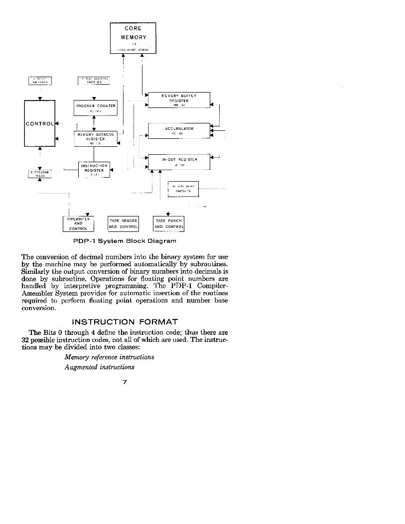
PDP-1 System Block Diagram
The conversion of decimal numbers into the binary system for use by the machine may be performed automatically by subroutines. Similarly the output conversion of binary numbers into decimals is done by subroutine. Operations for floating point numbers are handled by interpretive programming. The PDP-1 Compiler- Assembler System provides for automatic insertion of the routines required to perform floating point operations and number base conversion.
INSTRUCTION FORMAT The Bits 0 through 4 define the instruction code; thus there are
32 possible instruction codes, not all of which are used. The instruc- tions may be divided into two classes:
Memory reference instructions Augmented instructions
7

In the memory reference instructions, Bit 5 is the indirect address bit. The instruction memory address, Y, is in Bits 6 through 17. These digits are sufficient to address 4096 words of memory.
0’ INSTRUCTION w MEMORY ADDRESS, Y
of 0 z
I I I I I I I I I I I 0'1'213'4 5 6'7 '8 ~9'10'11~12'13'14~15'16'17
I I
PDP-1 Instruction Format
The augmented instructions use Bits 5 through 17, to specify variations of the basic instruction. For example, in the shift instruc- tion, Bit 5 specifies direction of shift, Bit 6 specifies the character of the shift (arithmetic or logical), Bits 7 and 8 enable the registers (01 = AC, 10 = IO, and 11 = both) and Bits 9 through 17 specify the number of steps.
INDIRECT ADDRESSING
A memory reference instruction which is to use an indirect ad- dress will have a ONE in Bit 5 of the instruction word. The original address, Y, of the instruction will not be used to locate the operand, jump location, etc., of the instruction, as is the normal case. Instead, it is used to locate a memory register whose contents in Bits 6 through 17 will be used as the address of the original instruction. Thus, Y is not the location of the operand but the location of the location of the operand. If the memory register containing the in- direct address also has a ONE in Bit 5, the indirect addressing pro- cedure is repeated and a third address is located. There is no limit to the number of times this process can be repeated.
OPERATING SPEEDS
Operating times of PDP-1 instructions are multiples of the mem- ory cycle of 5 microseconds. Two-cycle instructions refer twice to memory and thus require 10 microseconds for completion. Examples of this are add, subtract, deposit, load, etc. The jump, augmented and combined augmented instructions need only one call on memory and are performed in 5 microseconds.
In-Out Transfer instructions that do not include the optional wait function require 5 microseconds. If the in-out device requires a wait time for completion, the operating time depends upon the device being used.
8

Each step of indirect addressing requires an additional 5 micro- seconds.
MANUAL CONTROLS
The Console of PDP-1 has controls and indicators for the use of the operator. All computer flip-flops have indicator lights on the Console. These indicators are primarily for use when the machine has stopped or when the machine is being operated one step at a time. While the machine is running, the brightness of an indicator bears some relationship to the relative duty factor of that par- ticular flip-flop.
Three registers of toggle switches are available on the Console. These are the Data Field-Instruction Field-Address (18 bits), the Test Word (18 bits), and the Sense Switches (6 bits). The first two are primarily used in conjunction with the operating push buttons. The Sense Switches are present for manual intervention. The use of these switches is determined by the program.
Operating Push Buttons
Start The computer will start. The first instruction comes from the memory location indicated in the Field and Address Switches.
SbP
Continue
The computer will come to a halt at the com- pletion of the current memory cycle. The computer will resume operation starting at the state indicated by the lights.
Deposit
Read In
Examine The contents of the memory register indicated by the Field and Address Switches will be displayed in the Accumulator and the Memory Buffer lights. The word selected by the Test Word Switches will be put in the memory location indicated by the Field and Address Switches. The photoelectric punched tape reader will start operating in the Read-In mode.
Operating Toggle Switches
Power Single Step
Turns all power to the computer on and off. When the Single Step Switch is on, the com- puter will halt at the completion of each memory cycle. This switch is particularly use- ful in debugging programs. Repeated opera-
9
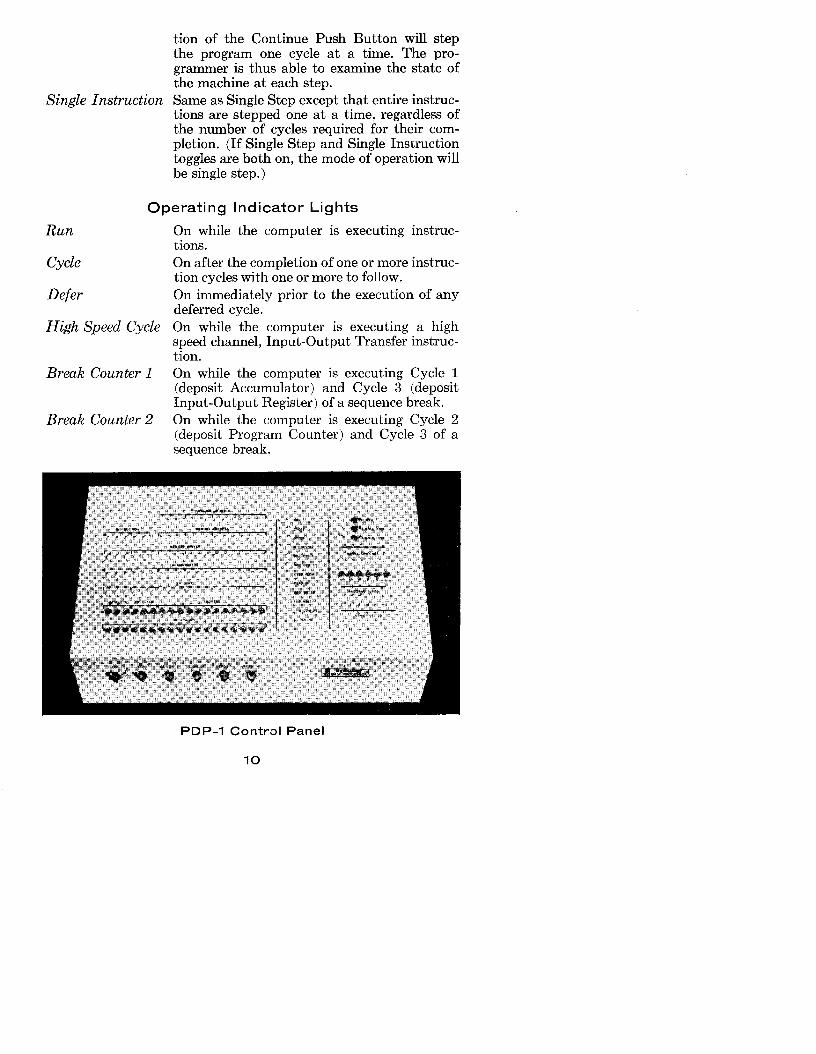
tion of the Continue Push Button will step the program one cycle at a time. The pro- grammer is thus able to examine the state of the machine at each step.
Single Instruction Same as Single Step except that entire instruc- tions are stepped one at a time, regardless of the number of cycles required for their com- pletion. (If Single Step and Single Instruction toggles are both on, the mode of operation will be single step.)
Operating Indicator Lights
Run
Cycle
Defer
High Speed Cycle
Break Counter 1
Break Counter 2
On while the computer is executing instruc- tions. On after the completion of one or more instruc- tion cycles with one or more to follow. On immediately prior to the execution of any deferred cycle. On while the computer is executing a high speed channel, Input-Output Transfer instruc- tion. On while the computer is executing Cycle 1 (deposit Accumulator) and Cycle 3 (deposit Input-Output Register) of a sequence break. On while the computer is executing Cycle 2 (deposit Program Counter) and Cycle 3 of a sequence break.
PDP-1 Control Panel

Overflow On if overflow has occurred. (Can only be turned off or cleared by executing the Skip on Zero Overflow instruction or pressing Start.)
Read In On while the computer is reading or trying to read punched tape in the Read-In mode.
Sequence Break On while the computer is using the Sequence Break System.
In-Out Halt On while the computer is executing a deferred Input-Output Transfer instruction.
In-Out Commands On while the computer is executing any Input- Output Transfer instruction.
In-Out Sync Used for maintenance purposes only.
Program Flags On after the computer has executed the Set Selected Program Flag instruction or an in-out device has been activated, indicating its readi- ness to be serviced. (Can only be turned off or cleared by executing the Clear Selected Pro- gram Flag instruction.)
Memory Field These indicate which memory field is currently in use.
Register Indicator Lights
Program Counter
Instruction
Memory Address
Memory Buffer
Accumulator
In-Out
Displays 12 bits which represent the address of the next instruction to be executed. Displays 5 bits which represent the basic operation code of the instruction being exe- cuted. Displays 12 bits which represent the address of the instruction being executed (after Cycle 1) or the address of the operand (after succeed- ing cycles). Displays 18 bits which represent the instruc- tion being executed (operation code and address part after Cycle 1) or the M-bit oper- and (after succeeding cycles). Displays 18 bits which represent the results of arithmetic and logical operations. Displays 18 bits which represent information just transferred in or out of the computer or the results of certain arithmetic and logical operations.
11

INSTRUCTION LIST
This list includes the title of the instruction, the normal execution time of the instruction, i.e., the time with no indirect address, the mnemonic code of the instruction, and the operation code number. In the following list, the contents of a register are indicated by C ( ). Thus C(Y) means the contents of memory at Address Y; C(AC) means the contents of the accumulator; C(I0) means the contents of the in-out register. An alphabetical and numerical listing of the instructions is contained on Pages 32 to 39.
Memory Reference Instructions
ARITHMETIC INSTRUCTIONS
Add (10 psec) add Y Operation Code 40 The new C(AC) are the sum of C(Y) and the original C (AC). The C(Y) are unchanged. The addition is performed with l’s complement arith- metic. If the sum exceeds the capacity of the Accumulator Register, the overflow flip-flop will be set (see Skip Group instructions).
Subtract (10 psec) sub Y Operation Code 42 The new C(AC) are the original C(AC) minus the C(Y). The C(Y) are unchanged. The subtraction is performed using l’s complement arith- metic. If the difference exceeds the capacity of the Accumulator, the over- flow flip-flop will be set (see Skip Group instructions).
Multiply Step (10 psec) mus Y Operation Code 54 If Bit 17 of the In-Out Register is a ONE, the C(Y) are added to C(AC). If IO Bit 17 is a ZERO, the addition does not take place. In either case, the C(AC) and C (IO) are shifted right one place. AC Bit 0 is made ZERO by this shift. This instruction is used in the multiply subroutine.
Divide Step (10 wet) dis Y Operation Code 56 The Accumulator and the In-Out Register are rotated left one place. IO Bit 17 receives the complement of AC Bit 0. If IO Bit 17 is ONE, the C(Y) are subtracted from C (AC). If IO Bit 17 is ZERO, C(Y) + 1 are added to C(AC). This instruction is used in the divide subroutine.
Index (10 psec) idx Y Operation Code 44 The C(Y) are replaced by C(Y) + 1. The C(Y) + 1 are left in the Ac- cumulator. The previous C(AC) are lost. Overflow is not indicated.
Index and Skip if Positive (10 psec) isp Y Operation Code 46 The C(Y) are replaced by C(Y) + 1. The C(Y) + 1 are left in the Ac- cumulator. The previous C(AC) are lost. If, after the addition, C(Y)
12
+ 1 are positive, the Program Counter is advanced one extra position and the next instruction in the sequence is skipped. Overflow is not indicated.
LOGICAL INSTRUCTIONS
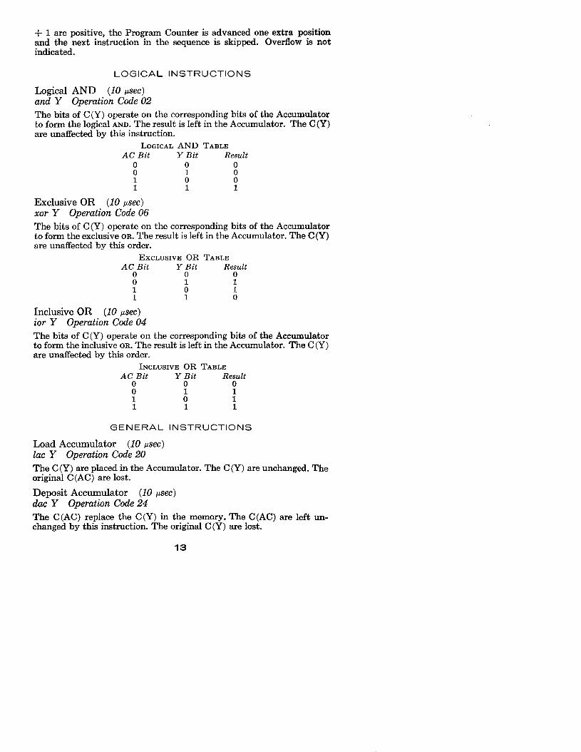
Logical AND (10 psec) and Y Operation Code 02 The bits of C(Y) operate on the corresponding bits of the Accumulator to form the logical AND. The result is left in the Accumulator. The C(Y) are unaffected by this instruction.
LOGICAL AND TABLE AC Bit Y Bit Result
0 0 0 0
: k : 1 1
Exclusive OR (10 psec) xor Y Operation Code 06 The bits of C(Y) operate on the corresponding bits of the Accumulator to form the exclusive OR. The result is left in the Accumulator. The C(Y) are unaffected by this order.
EXCLUSIVE OR TABLE
AcOBit Y Bit Result
0 0
Y A : 1 1 0
Inclusive OR (10 psec) ior Y Operation Code 04 The bits of C(Y) operate on the corresponding bits of the Accumulator to form the inclusive OR. The result is left in the Accumulator. The C(Y) are unaffected by this order.
INCLUSIVE OR TABLE AC Bit Y Bit Result
x 0 0
1 i 1' 1 1 1
GENERAL INSTRUCTIONS
Load Accumulator (10 psec) lac Y Operation Code 20 The C(Y) are placed in the Accumulator. The C(Y) are unchanged. The original C(AC) are lost.
Deposit Accumulator (10 psec) dac Y Operation Code 24 The C(AC) replace the C(Y) in the memory. The C(AC) are left un- changed by this instruction. The original C(Y) are lost.
13

Deposit Address’Part (IO psec) dap Y Operation Code 26 Bits 6 through 17 of the Accumulator replace the corresponding digits of memory register Y. C (AC) are unchanged as are the contents of Bits 0 through 5 of Y. The original contents of Bits 6 through 17 of Y are lost.
Deposit Instruction Part (10 ksec) dip Y Operation Code 30 Bits 0 through 5 of the Accumulator replace the corresponding digits of memory register Y. The Accumulator is unchanged as are Bits 6 through 17 of Y. The original contents of Bits 0 through 5 of Y are lost.
Load In-Out Register (10 psec) lio Y Operation Code 22 The C(Y) are placed in the In-Out Register. C(Y) are unchanged. The original C(I0) are lost.
Deposit In-Out Register (10 psec) dio Y Operation Code 32 The C (IO) replace the C (Y) in memory. The C (IO) are unaffected by this instruction. The original C(Y) are lost.
Deposit Zero in Memory (10 lsec) dzm Y Operation Code 34 Clears (sets equal to plus zero) the contents of register Y.
Execute (5 psec plus time of instruction executed) xct Y Operation Code 10 The instruction located in register Y is executed. The Program Counter remains unchanged (unless a jump or skip were executed). Execute may be indirectly addressed, and the instruction being executed may use in- direct addressing. An xct instruction may execute other xct commands.
Jump (5 crsec) jmp Y Operation Code 60 The Program Counter is reset to Address Y. The next instruction that will be executed will be taken from Memory Register Y. The original contents of the Program Counter are lost.
Jump and Save Program Counter (5 psec) jsp Y Operation Code 62
The contents of the Program Counter are transferred to the Accumulator. When the transfer takes place, the Program Counter holds the address of the instruction following the jsp. The Program Counter is then reset to Address Y. The next instruction that will be executed will be taken from Memory Register Y. The original C(AC) are lost.
Call Subroutine (10 psec) cal Y Operation Code 16 The address part of the instruction, Y, is ignored. The contents of the Accumulator are deposited in Memory Register 100. The contents of the
14

Program Counter (holding the address of the instruction following the ccl) are transferred to the Accumulator. The next instruction that will be executed is taken from Memory Register 101. This instruction requires that the indirect bit be ZERO. The instruction may be used as part of a master routine to call subroutines.
Jump and Deposit Accumulator (10 psec) jda Y Operation Code 17 The contents of the Accumulator are deposited in Memory Register Y. The contents of the Program Counter (holding the address of the instruc- tion following thejda) are transferred to the Accumulator. The next in- struction that will be executed is taken from Memory Register Y + 1. This instruction requires that the indirect bit be a ONE. The instruc- tion is equivalent to the instructions due Y, followed by jsp Y + 1.
Skip if Accumulator and Y differ (IO psec) sad Y Operation Code 50 The C(Y) are compared with the C(AC). If the two numbers are differ- ent, the Program Counter is indexed one extra position and the next in- struction in the sequence is skipped. The C(AC) and the C(Y) are un- affected by this operation.
Skip if Accumulator and Y are the same (10 ~sec) sas Y Operation Code 52 The C(Y) are compared with the C(AC). If the two numbers are identi- cal, the Program Counter is indexed one extra position and the next in- struction in the sequence is skipped. The C (AC) and C(Y) are unaffected by this operation.
Augmented Instructions Load Accumulator with N (5 psec) law N Operation Code 70 The number in the memory address bits of the instruction word is placed in the Accumulator. If the indirect address bit is ONE, the complement of N (- N) is put in the Accumulator.
Shift Group (5 E.csec) sft Operation Code 66 This group of instructions will rotate or shift the Accumulator and/or the In-Out Register. When the two registers operate combined, the In- Out Register is considered to be an 18-bit magnitude extension of the right end of the Accumulator.
Rotate is a non-arithmetic cyclic shift. That is, the two ends of the register are logically tied together and information is rotated as though the register were a ring.
Shift is an arithmetic operation and is, in effect, multiplication of the number in the register by 2 *N, where N is the number of shifts; plus is left and minus is right.
The number of shift or rotate steps to be performed (N) is indicated by the number of ONE'S in Bits 9 thru 17 of the instruction word. Thus, Rotate Accumulator Right nine times is 671777. A shift or rotate of one place can be indicated nine different ways. The usual convention is to use the right end of the instruction word (rar I = 671001).
15
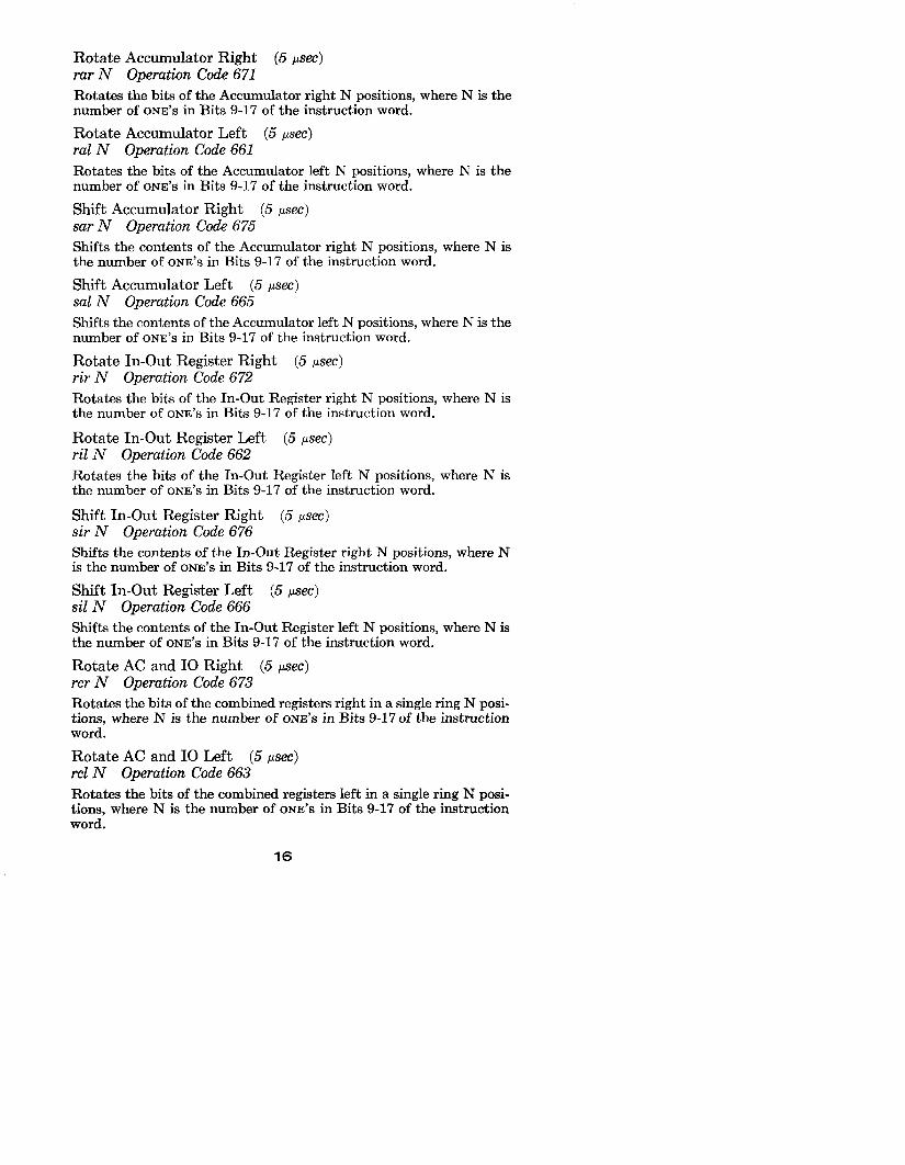
Rotate Accumulator Right (5 psec) rar N Operation Code 671 Rotates the bits of the Accumulator right N positions, where N is the number of ONE'S in Bits 9-17 of the instruction word.
Rotate Accumulator Left (5 psec) ral N Operation Code 661 Rotates the bits of the Accumulator left N positions, where N is the number of ONE'S in Bits 9-17 of the instruction word.
Shift Accumulator Right (5 Fsec) sar N Operation Code 675 Shifts the contents of the Accumulator right N positions, where N is the number of ONE'S in Bits 9-17 of the instruction word.
Shift Accumulator Left (5 psec) sal N Operation Code 665 Shifts the contents of the Accumulator left N positions, where N is the number of ONE'S in Bits 9-17 of the instruction word.
Rotate In-Out Register Right (5 psec) rir N Operation Code 672 Rotates the bits of the In-Out Register right N positions, where N is the number of ONE'S in Bits 9-17 of the instruction word.
Rotate In-Out Register Left (5 psec) ril N Operation Code 662 Rotates the bits of the In-Out Register left N positions, where N is the number of ONE'S in Bits 9-17 of the instruction word.
Shift In-Out Register Right (5 psec) sir N Operation Code 676 Shifts the contents of the In-Out Register right N positions, where N is the number of ONE'S in Bits 9-17 of the instruction word.
Shift In-Out Register Left (5 psec) sil N Operation Code 666 Shifts the contents of the In-Out Register left N positions, where N is the number of ONE'S in Bits 9-17 of the instruction word.
Rotate AC and IO Right (5 psec) rcr N Operation Code 673 Rotates the bits of the combined registers right in a single ring N posi- tions, where N is the number of ONE'S in Bits 9-17 of the instruction word.
Rotate AC and IO Left (5 psec) rcl N Operation Code 663 Rotates the bits of the combined registers left in a single ring N posi- tions, where N is the number of ONE'S in Bits 9-17 of the instruction word.
16

Shift AC and IO Right (5 psec) SW N Operation Code 677 Shifts the contents of the combined registers right N positions, where N is the number of ONE'S in Bits 9-17 of the instruction word.
Shift AC and IO Left (5 Met) scl N Operation Code 667 Shifts the contents of the combined registers left N positions, where N is the number of ONE'S in Bits 9-17 of the instruction word.
Skip Group (5 psec) skp Operation Code 64
This group of instructions senses the state of various flip-flops and switches in the machine. The address portion of the instruction selects the particular function to be sensed. All members of this group have the same operation code.
The instructions in the Skip Group may be combined to form the in- clusive OR of the separate skips. Thus, if Address 3000 is selected, the skip would occur if the overflow flip-flop equals ZERO or if the In-Out Register is positive. The combined instruction would still take 5 micro- seconds.
The intent of any skip instruction can be reversed by making Bit 5 (normally the Deferred Address Bit) equal to ONE. For example, the Skip on Zero Accumulator instruction, if deferred, becomes Do Not Skip on Zero Accumulator.
Skip on ZERO Accumulator (5 psec) sza Address 100 If the Accumulator is equal to plus ZERO (all bits are ZERO), the Pro- gram Counter is advanced one extra position and the next instruction in the sequence is skipped.
Skip on Plus Accumulator (5 psec) spa Address 200 If the sign bit of the Accumulator is ZERO, the Program Counter is ad- vanced one extra position and the next instruction in the sequence is skipped.
Skip on Minus Accumulator (5 psec) sma Address 400 If the sign bit of the Accumulator is ONE, the Program Counter is ad- vanced one extra position and the next instruction in the sequence is skipped.
Skip on ZERO Overflow (5 psec) szo Address 1000 If the overflow flip-flop is a ZERO, the Program Counter is advanced one extra position and the next instruction in the sequence will be skipped. The overflow flip-flop is cleared by the instruction. This flip-flop is set by an addition or subtraction that exceeds the capacity of the Accumu- lator. The overflow flip-flop is not cleared by arithmetic operations which do not cause an overflow. Thus, a whole series of arithmetic operations can be checked for correctness by a single szo. The overflow flip-flop is cleared by the “Start” Switch.
17

Skip on Plus In-Out Register (5 psec) spi Address 2000 If the sign digit of the In-Out Register is ZERO, the Program Counter is indexed one extra position and the next instruction in sequence is skipped.
Skip on ZERO Switch (5 psec) szs Addresses 10, 20. . . . .70 If the selected Sense Switch is ZERO, the Program Counter is advanced one extra position and the next instruction in the sequence will be skipped. Address 10 senses the position of Sense Switch 1, Address 20 Switch 2, etc. Address 70 senses all the switches. If 70 is selected all 6 switches must be ZERO to cause the skip.
Skip on ZERO Program Flag (5 psec) szf Addresses 0 to 7 inclusive If the selected program flag is a ZERO, the Program Counter is ad- vanced one extra position and the next instruction in the sequence will be skipped. Address 0 is no selection. Address 1 selects Program Flag 1, etc. Address 7 selects all program flags. All flags must be ZERO to cause the skip.
Operate Group (5 psec) opr Operation Code 76
This instruction group performs miscellaneous operations on various Central Processor Registers. The address portion of the instruction speci- fies the action to be performed.
The instructions in the Operate Group can be combined to give the union of the functions. The instruction opr 3200 will clear the AC, put TW to AC, and complement AC. If the number minus zero is interpreted as an instruction, the IO is cleared, AC gets the complement of the TW switches, all program flags are set and the computer halts.
Clear In-Out Register (5 psec) cli Address 4000 Clears (sets equal to plus zero) the In-Out Register.
Load Accumulator from Test Word (5 psec) lat Address 2000 Forms the inclusive OR of the C(AC) and the contents of the Test Word. This instruction is usually combined with Address 200 (Clear Accumulator), so that C (AC) will equal the contents of the Test Word Switches.
Complement Accumulator (5 psec) cma Address 1000 Complements (makes negative) the contents of the Accumulator.
Halt hlt Address 400 Stops the computer.
18

Clear Accumulator (5 psec) cla Address 200 Clears (sets equal to plus zero) the contents of the Accumulator.
Clear Selected Program Flag (5 wet) elf Address 01 to 07 inclusive Clears the selected program flag. Address 01 clears Program Flag 1, 02 clears Program Flag 2, etc. Address 07 clears all program flags.
Set Selected Program Flag (5 psec) stf Addresses 11 to 17 inclusive Sets the selected program flag. Address 11 sets Program Flag 1; 12 sets Program Flag 2, etc. Address 17 sets all program flags.
No Operation (5 psec) nop Address 0000 The state of the computer is unaffected by this operation, and the Program Counter continues in sequence.
In-Out Transfer Group (5 psec without in-out wait) iot Operation Code 72
The variations within this group of instructions perform all the in-out control and information transfer functions. If Bit 5 (normally the In- direct Address bit) is a ONE, the computer will halt and wait for the com- pletion pulse from the device activated. When this device delivers its completion, the computer will resume operation of the instruction se- quence.
An incidental fact which may be of importance in certain scientific or real time control applications is that the time origin of operations follow- ing an in-out completion pulse is identical with the time of that pulse.
Most in-out operations require a known minimum time before com- pletion. This time may be utilized for programming. The appropriate In-Out Transfer is given with no in-out wait (Bit 5 a ZERO and Bit 6 a ONE). The instruction sequence then continues. This sequence must include an iot instruction 730000 which performs nothing but the in-out wait, and the instruction must occur before the safe minimum time. A table of minimum times for all in-out devices is delivered with the computer: it lists minimum time before completion pulse and minimum In-Out Register free time.
Bit 6 determines whether a completion pulse will or will not be re- ceived from the in-out device. When it is different than Bit 5, a comple- tion pulse will be received. When it is the same as Bit 5, a completion pulse will not be received.
In addition to the control functions of Bits 5 and 6, Bits 7 through 11 are also used as control bits serving to extend greatly the power of the iot instructions. For example, Bits 12 through 17, which are used to desig- nate a class of input or output devices such as typewriters, may be further defined by Bits 7 through 11 as referring to Typewriter 1, 2, 3, etc., and whether or not the Sequence Break System is to be used.
19

CENTRAL PROCESSOR OPTIONS
STANDARD PDP-,
CENTRAL MACHINE
WlTH COMM”NlCATlON FOR PERIPHERAL OEYICES
AND OPTIONS
INPUT-OUTPUT OPTIONS NOTE
OUTER NUMBERS DENOTE OPTION TYPES
*ONLY ONE OPTION MAY BE CONNECTED FOR A MACHINE
PDP-1 System Configuration Diagram
20 21

III. STANDARD AND OPTIONAL EQUIPMENT
STANDARD EQUIPMENT
Punched Tape Reader The punched tape reader of the PDP-1 is a photoelectric device capable of reading 400 lines per second. Three lines form the standard B-bit word when reading binary punched eight-hole tape. Five, six, and seven- hole tape may also be read.
Read Punched Tape, Alphanumeric rpa Address 0001 In this mode, one line of tape is read for each In-Out Transfer. All eight holes of the line are read. The information is left in the right eight bits of the In-Out Register, the remainder of the register being left clear.
The code of the off-line tape preparation typewriter (Friden FIO-DEC Recorder-Reproducer) contains an odd parity bit. This bit may be checked by the read-in program. The FIO-DEC Code can then be converted to the concise six-bit code used by PDP-1 merely by drop- ping the eighth bit (parity). A list of characters and their FIO-DEC and Concise Codes is found on Pages 37 through 39.
High Speed Punched Tape Reader

Read Punched Tape, Binary rpb Address 0002 For each In-Out Transfer instruction, three lines of punched tape are read and assembled in the In-Out Register to form a full computer word. For a line to be recognized in this mode, the eighth hole must be punched; i.e., lines with no eighth hole will be skipped over. The seventh hole is ignored. The pattern of holes in the binary tape is ar- ranged so as to be easily interpreted visually in terms of machine instruction.
Read Reader Buffer rrb Address 0030 When operating in the Sequence Break Mode, the rpa and rpb in- structions operate as usual but do not transfer information from the reader buffer to the IO Register. To accomplish the transfer, these instructions must be followed by an rrb instruction.
Read-In Mode This is a special mode activated by the “Read-In” switch on the con- sole. It provides a means of entering programs which neither rely on programs in memory nor require a plug board. Pushing the “Read- In” switch starts the reader in the binary mode. The first group of three lines, and alternate succeeding groups of three lines, are inter- preted as ‘?Read-In” mode instructions. Even-numbered groups of three lines are data. The “Read-In” mode instructions must be either “deposit in-out” (die Y) or “jump” (jmp Y). If the instruction is dio Y, the next group of three binary lines will be stored in memory loca- tion Y and the reader continues moving. If the instruction is jmp Y, the “Read-In” mode is terminated, and the computer will commence operation at the address of the jump instruction.
Punched Tape Punch
The standard PDP-1 punched tape punch operates at a speed of 63 lines per second. It can operate in either the alphanumeric mode or the binary mode.
Punch Punched Tape, Alphanumeric ppa Address 0005 For each In-Out Transfer instruction one line of tape is punched. In- Out Register Bit 17 conditions Hole 1. Bit 16 conditions Hole 2, etc. Bit 10 conditions Hole 8.
Punch Punched Tape, Binary ppb Address 0006 For each In-Out Transfer instruction one line of tape is punched. In- Out Register Bit 5 conditions Hole 1. Bit 4 conditions Hole 2, etc. Bit 0 conditions Hole 6. Hole 7 is left blank. Hole 8 is always punched in this mode.
23

Alphanumeric Typewriter The typewriter will operate in the input mode or the output mode.
Type Out tyo Address 0003 For each In-Out Transfer instruction one character is typed. The character is specified by the right six bits of the In-Out Register.
Type In tyi Address 0004 This operation is completely asynchronous and is therefore handled differently than any of the preceding in-out operations. When a typewriter key is struck, Program Flag 1 is set. At the same time the code for the struck key is presented to gates connected to the right six bits of the In-Out Register. This information will remain at the gate for a relatively long time by virtue of the slow mechanical action. A program designed to accept typed-in data would periodically check the status of Program Flag 1. If at any time Program Flag 1 is found to be set, an In-Out Transfer instruction with Address 4 must be executed for information to be transferred. This In-Out Transfer should not use the optional in-out halt. The information contained in the typewriter’s coder is then read into the right six bits of the In-Out Register. The tyi instruction automatically clears the IO before trans- ferring the information. The tyi instruction is usually preceded by a Clear Selected Program Flag 1 instruction.
Sequence Break Mode
Two instructions are associated directly with the One-Channel Sequence Break System on the standard PDP-1.
Enter Sequence Break Mode esm Address 0055 This instruction turns on the Sequence Break System, allowing automatic interrupts to the main sequence to occur. The contents of the Sequence Break flip-flops are unaffected by this instruction.
Leave Sequence Break Mode lsm Address 0054 This instruction turns off the Sequence Break System, thus prevent- ing interrupts to the main sequence. Should interrupts occur while the System is off, the Sequence Break flip-flops will, nevertheless, continue to be set.
Miscellaneous
Check Status cks Address 0033 This instruction checks the status of various in-out devices and sets IO Bits 0 through 4 for subsequent program interrogation as follows:
24

IO Bit Positions If ONE
0 Displayed point sensed by light pen 1 Punched tape reader busy 2 3
Typewriter busy y Typewriter key stuck
4 Punched tape punch busy
OPTIONAL EQUIPMENT
Automatic Multiply and Divide (Type 10) This option replaces the Multiply Step and Divide Step instructions with the following instructions:
Multiply (14 to 25 psec) mu1 Y Operation Code 54 The product of C (AC) and C(Y) is formed in the AC and IO registers. The sign of the product is in the AC sign bit. IO Bit 17 also contains the sign of the product. The magnitude of the product is the 34-bit string from AC Bit 1 through IO Bit 16. The C(Y) are not affected by this instruction.
Divide (30 to 40 psec, except on overflow, 12 psec) div Y Operation Code 56 The dividend must be in the AC and IO registers in the form indicated in the instruction, Multiply. IO Bit 17 is ignored. The divisor is the C(Y). At the completion of the instruction, the C (AC) are the quotient and the C (IO) are the remainder. The sign of the remainder is the sign of the dividend. If an overflow were to occur, the division does not take place, the C(AC) and C(I0) are unchanged, and the overflow indicator is set. The C(Y) are not affected by this instruction.
Memory Module (Type 12) Each Memory Module consists of 4096 18-bit words. A maximum of eight modules may be connected to the PDP-1.
Memory Field Control (Type 13) This control allows for memory expansion up to 16,384 18-bit words (i.e., four 4096-word memory modules). Each memory module is defined as consisting of two 2048-word fields. A select memory instruc- tion, jump field according to the C(Y), jfd Y, selects any two fields to be connected to the PDP-1 and jumps to a specified location in one of the two fields.
A second instruction, change fields according to Y, cfd Y, replaces the contents of the two 3-bit field registers with Bits 6 through 11 of the cfd instruction. The Program Counter is unaffected and computation continues in sequence using the newly selected fields.
When High Speed Channel transfers are involved, the high speed ehannel specifies a 1Cbit address for one of 16,384 words.
25
Memory Field Control (Type 14) This control allows for memory expansion up to 32,768 18-bit words (i.e., eight 4096-word memory modules). Each memory module repre- sents either a 4096 word Instruction Field or a 4096 word Data Field. A select memory instruction, jump field according to the C(Y), jfd Y, selects any two fields (one Instruction Field and one Data Field) to be connected to the PDP-1 and jumps to a specified location in the newly selected Instruction Field. A second instruction, change data field according to Y, cdf Y, replaces the contents of the 3-bit Data Field Register with Bits 9 through 11 of the cdf instruction. The Program Counter and the Instruction Field Register are unaffected, and computation continues in sequence using the same Instruction Field. When High Speed Channel transfers are involved, the high speed channel specifies a l&bit address for one of 32,768 words.
High Speed Channel (Type 19) The High Speed Channel is used to transfer blocks of words between memory and an in-out device, usually a high speed device such as magnetic tape. Such a channel is installed with the Tape Control Unit Type 52 or may be installed separately for special applications. As many as three High Speed Channels may be added to the PDP-1. Each of these is automatically interrogated at the completion of each memory cycle on a priority basis. The priority is wired and fixed. The Sequence Break System has an over-all priority just below that of the lowest priority High Speed Channel. When wired to this channel, a device communicates directly with memory through the Memory Buffer Register, bypassing the IO Register. After proper initiation, data transfers proceed without disturbing the main program. If the channel has a word for or needs a word from the memory, the current program sequence pauses for one memory cycle in order to serve that channel, then continues.
Sequence Break System (Type 20) An optional in-out control is available for PDP-1. This control, termed the Sequence Break System, allows concurrent operation of several in-out devices and the main sequence. The system has, nominally, 16 automatic interrupt channels arranged in a priority chain. A break to a particular sequence may be initiated by the completion of an in-out device, the program or any external signal. If this se- quence has priority, the C(AC), C(IO), C(PC), and the contents of the memory field flip-flops (if present) are stored in adjacent fixed locations unique to that sequence. The Program Counter is reset to the address contained in a fourth fixed location. The program is now operating in the new sequence. This new sequence may be broken by a higher priority sequence. A typical program loop for handling an in-out sequence would contain three to five instructions, including the appropriate iot. These are followed by load AC and load IO from the fixed locations and an indirect jump to location of the previous C (PC). This last instruction terminates the sequence. The Sequence Break System provides PDP-1 with much of the power of a multiple sequence machine or of a computer having in-out synchronizers or automatic trunks.
26

Cathode Ray X-Y Point Plotter
Visual CRT Display (Type 30) The PDP-1 cathode ray tube display is useful for presentation of graphical or tabular data to the operator. For each Display instruction (730007), one point is displayed. The first 10 bits of the IO Register, Bits 0 through 9, are the Y coordinate of the point. Bits 0 through 9 of the Accumulator are the X coordinate of the point.
27

Information is displayed at a rate of 20,000 points per second, and the resolution is 1 part in 1024.
Cathode Ray Tube Display
Precision CRT Display (Type 31) The operation of this 5-inch cathode ray tube display is similar to that of the Type 30. The resolution is 1 part in 4096. It comes equipped with mounting bezel to accept a camera or a photomultiplier device.
Light Pen (Type 32) This accessory allows information to be “written” on the cathode ray tube. The pen detects displayed information, and the pen output sets a program flip-flop in the machine each time a pulse of light strikes the pen.
Card Punch Control (Type 40-523) This control allows for on-line operation of standard card punching equipment. It contains an go-bit buffer which is loaded from the IO Register, using an iot instruction for each card row punched. The control is for use with a 523 Summary Punch at speeds of 100 cards per minute.
Card Reader Control (Type 41-523) This control provides for on-line operation of standard card reading equipment. It allows the read brush outputs to be directed to the IO Register. The control is for use with a 523 Summary Punch at speeds of 100 cards per minute.
28
Tape Transport (Type 50) This transport is compatible with IBM tape formats with a recording density of 200 7-bit characters per inch and an inter-record gap of x inch. The transfer rate is 15,000 characters per second at a tape speed of 75 inches per second. The method of recording is non-return- to-zero. A maximum of 24 tape transports may be connected to the PDP-1.
Programmed Tape Control Unit (‘Type 51) This control transfers information between the computer and the tape one character at a time. All transfer operations, including timing, error checking and assembly of characters into computer words are performed by routines. The Type 51 allows a choice of tape format, including the standard IBM tape format described under Tape Transport (Type 50).
Automatic Tape Control Unit (Type 52)
This control automatically transfers information between the com- puter memory and the tape in variable-length blocks of characters. It allows computation to continue while the transfer is in process by using the High Speed Channel, which is part of the control unit. Special features include scatter-read and gather-write; automatic, bit-by-bit read-compare with core memory; automatic parity error detection while reading and writing; and rapid tape searching through its ability to skip a pre-selected number of blocks. Tape format is standard IBM as described under Tape Transport (Type 50).
Programmed Line Printer and Control (Type 61) This is an on-line printing station capable of operating at 150 lines per minute (120 columns per line with 64 characters per column). All transfer operations, formatting and control functions are under program control.
Automatic Line Printer and Control (Type 62) This is an on-line printing station capable of operating at 600 lines per minute (120 columns per line with 64 characters per column). A simple one-line buffer is used. The appropriate iot instruction is repeated to fill the buffer. The order to print is then given. Following the comple- tion of the line print, the printer returns a completion pulse and spaces the paper.
Real Time Clock
A special input register may be connected to operate as a real time clock. This is a counting register operated by a crystal controlled oscillator.
The state of this counter may be read at any time by the appropriate In-Out Transfer instruction. The computer stops only long enough to provide synchronization with the clock oscillator, then resumes opera- tion in phase with it.
29

IV. PROGRAM LIBRARY
The Basic Program Library for PDP-1 is designed to provide the nucleus of a growing system of programs and subroutines. Among the programs in use are:
DECAL
Digital Equipment Compiler, Assembler and Linking Loader is an integrated program for PDP-1 incorporating in one system all of the essential features of advanced compilers, assemblers and loaders. The outstanding features of DECAL are:
l Open-Ended Programming System. DECAL can be modified without a detailed understanding of its internal operation by means of a recursive definition facility based on a skeleton com- piler with a basic set of logical capabilities. The skeleton compiler can act as a bootstrap for implementing additional features or deleting or changing existing facilities.
l Efficient Use of Storage Capacity. All available memory space will be used before DECAL runs out of space. This is accom- plished by means of a single table that meets all of the storage needs of DECAL. When any feature of DECAL is removed, all of the associated space is again made available.
l Eficient Use of Time. DECAL processing takes full advantage of the speeds of the standard PDP-1 input-output equipment (400 lines per second reader and 63 lines per second punch).
l One Pass Compiler-Assembler. The symbolic tape (usually pre- pared off-line) is only read one time. It is not stored in memory. A relocatable tape ready for the linking loader is punched as the symbolic tape is read.
l Eficient Object Program. Since DECAL allows compiler and assembler statements to be freely intermixed at the discretion of the programmer, the object program can be as efficient as desired.
l Variable Length Symbols. Symbol lengths are not restrictive and can be hundreds of characters long if necessary.
l Program Integration and Relocation. At load time, individual routines and subroutines can be loaded in any order. All cross- referencing is done automatically, and the resulting program is arranged compactly starting at any specified origin. The names of subroutines required at run time and not yet loaded are listed on the typewriter so that they may be subsequently loaded.
l Use of ALGOL. DECAL includes that part of ALGOL which is compatible with the PDP-1 Computer. Compiler (algebraic)
30

and assembler statements can be written taking full advantage of the ALGOL reference language due to the unique character set used by the PDP-1.
a Recursively Defined Macro Instructions. Full use of such complex items as recursively defined macro instructions can be made when writing DECAL assembler statements.
l Use of Arbitrary Languages. Arbitrary reference languages can be defined and incorporated into DECAL to handle special problems.
l Use of Floating Point Systems. DECAL-compatible, single and double precision floating point systems can be incorporated.
l Generalized subscripting, indexing and address arithmetic facilities can be incorporated.
OTHER PROGRAMS
FRAP Assembly Program is a basic assembler designed to oper- ate with a very minimum amount of internal storage.
Standard Function Generator Subroutines for single precision fixed point arithmetic. These include: sine, cosine, arctangent, square root, exponential and logarithmic subroutines.
Single Precision Floating Point Package for arithmetic using an M-bit fraction and an H-bit exponent. The package includes standard function generator subroutines.
Double Precision Floating Point Package for arithmetic using a 36-bit fraction and an H-bit exponent. The package includes standard function generator subroutines.
Basic Double Precision Fixed Point Subroutines including addi- tion, subtraction, multiplication and division.
Utility Routine Package including a wide range of input-output subroutines and debugging aids.
31
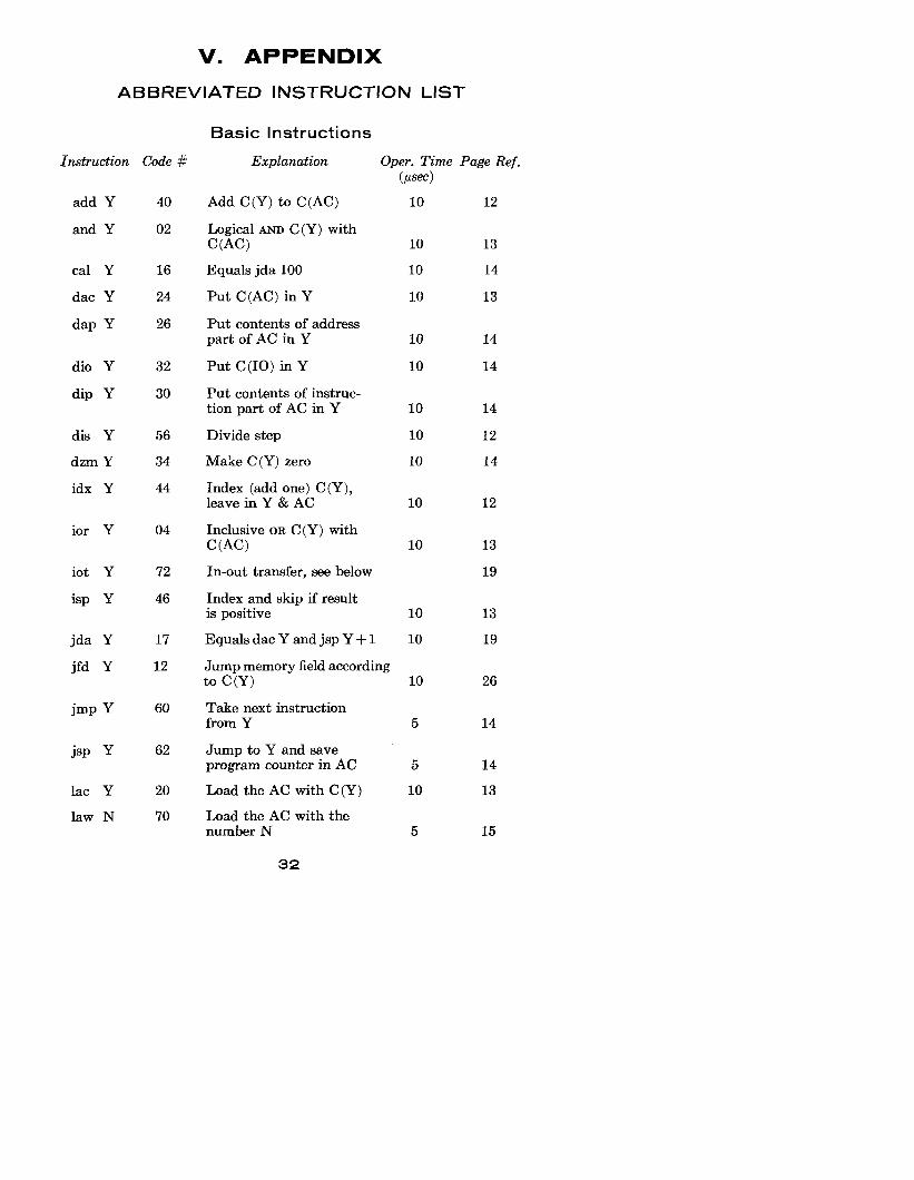
V. APPENDIX
ABBREVIATED INSTRUCTION LIST
Basic Instructions
Instruction Code # Explanation
add Y
and Y
40
02
cal Y 16
dac Y 24
dap Y 26
di0 Y 32
dip Y 30
dis Y 56
dzm Y 34
idx Y 44
Ada C(Y) to C(AC)
Logical AND C(Y) with COW
Equals jcla 100
Put C(AC) in Y
Put contents of address part of AC in Y
Put C(I0) in Y
Put contents of instruc- tion part of AC in Y
Divide step
Make C(Y) zero
Index (add one) C(Y), leave in Y & AC
ior Y 04 Inclusive OR C(Y) with C(AC)
iot Y 72
isp Y 46
jcla Y
jfd Y
17
12
jmp Y 60
jsp Y 62
lac Y
law N
20
70
In-out transfer, see below
Index and skip if result is positive 10
Equals dac Y and jsp Y + 1 10
Jump memory field according to C(Y) 10
Take next instruction from Y 5
Jump to Y and save program counter in AC 5
Load the AC with C(Y) 10
Load the AC with the number N 5
32
Oper. Time Page Ref. (wet)
10
10
10
10
10
10
10
10
10
10
10
12
13
14
13
14
14
14
12
14
12
13
19
13
19
26
14
14
13
15
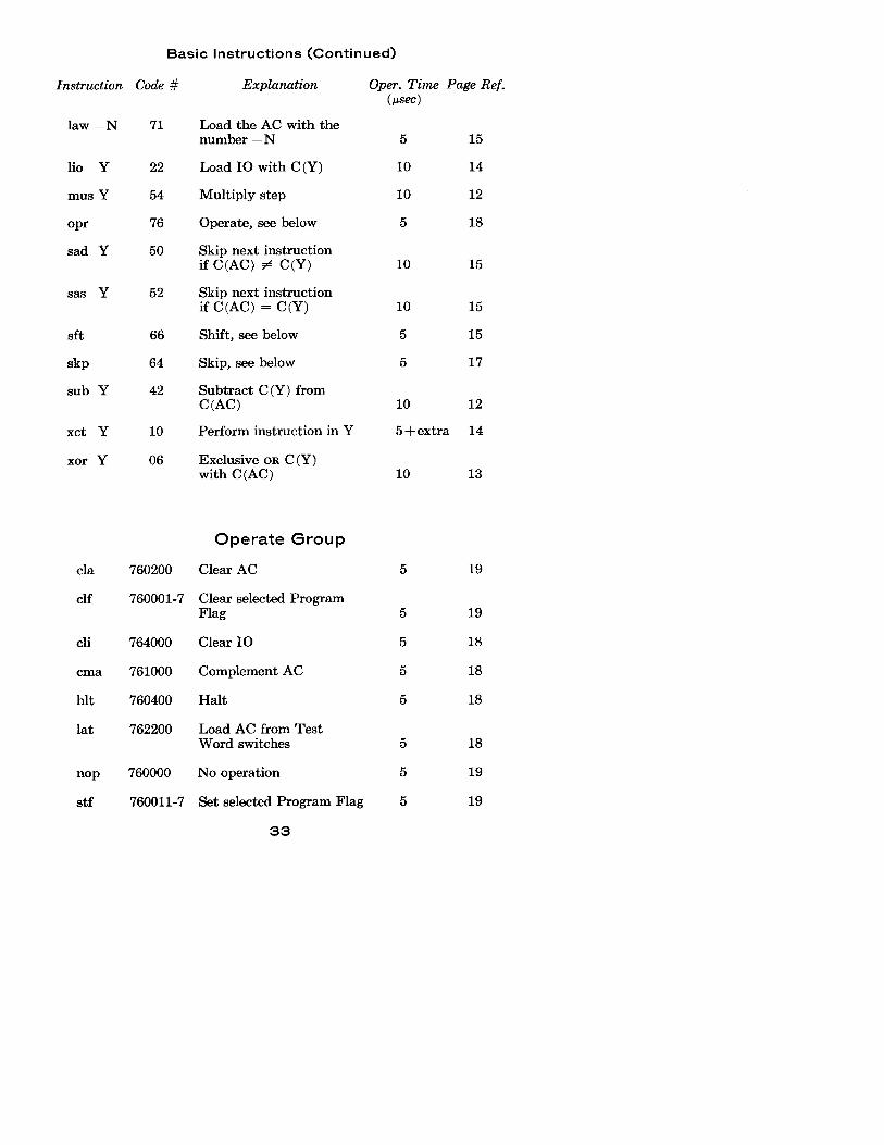
Basic Instructions (Continued)
Instruction Code # Explanation Oper. Time Page Ref.
law-N 71
ho Y 22
mus Y 54
opr 76
sad Y 50
sas Y 52
sft 66
skp 64
sub Y 42
xct Y 10
xor Y 06
cla 760200
elf 760001-7
cli 764060
cma 761000
hlt 760400
lat 762200
nw
stf
760000
760011-7
Load the AC with the number - N
Load IO with C(Y)
Multiply step
Operate, see below
Skip next instruction if C(AC) # C(Y)
Skip next instruction if C(AC) = C(Y)
Shift, see below
Skip, see below
Subtract C(Y) from CW)
Perform instruction in Y
Exclusive OR C(Y) with C(AC)
Operate Group
Clear AC
Clear selected Program Flag
Clear IO
Complement AC
Halt
Load AC from Test Word switches
No operation
Set selected Program Flag
5 15
10 14
10 12
5 18
10 15
10 15
5 15
5 17
10 12
5+extra 14
10 13
5 19
5 19
5 18
5 18
5 18
5 18
5 19
5 19
33
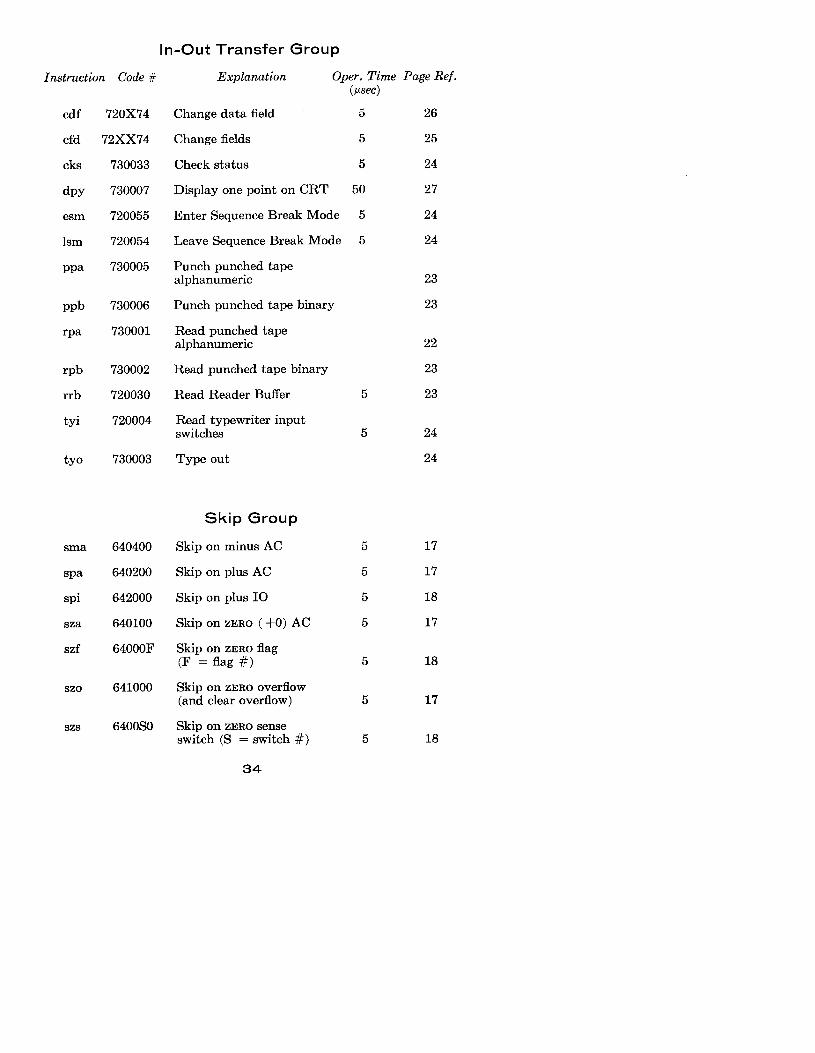
In-Out Transfer Group
Instruction Code # Explanation Oper. Time Page Ref.
cdf 720X74
cfd 72Xx74
CkS 730033
dpy 730007
esm 720055
lsm 720054
wa 730005
ppb 730006
w 730001
vb 730002
rrb 720030
tyi 720004
tY0 730003
sma 640400
spa 640200
spi 642000
sza 640100
szf 64000F
szo
szs
641000
6400S0
Change data field
Change fields
Check status
Display one point on CRT
Enter Sequence Break Mode
Leave Sequence Break Mode
Punch punched tape alphanumeric
Punch punched tape binary
Read punched tape alphanumeric
Read punched tape binary
Read Reader Buffer
Read typewriter input switches
Type out
Skip Group
Skip on minus AC
Skip on plus AC
Skip on plus IO
Skip on ZERO ( +0) AC
Skip on ZERO flag (F = flag #I
Skip on ZERO overflow (and clear overflow)
Skip on ZERO sense switch (S = switch #)
34
(wet)
5
5
5
50
5
5
26
25
24
27
24
24
23
23
22
23
23
24
24
17
17
18
17
18
17
18
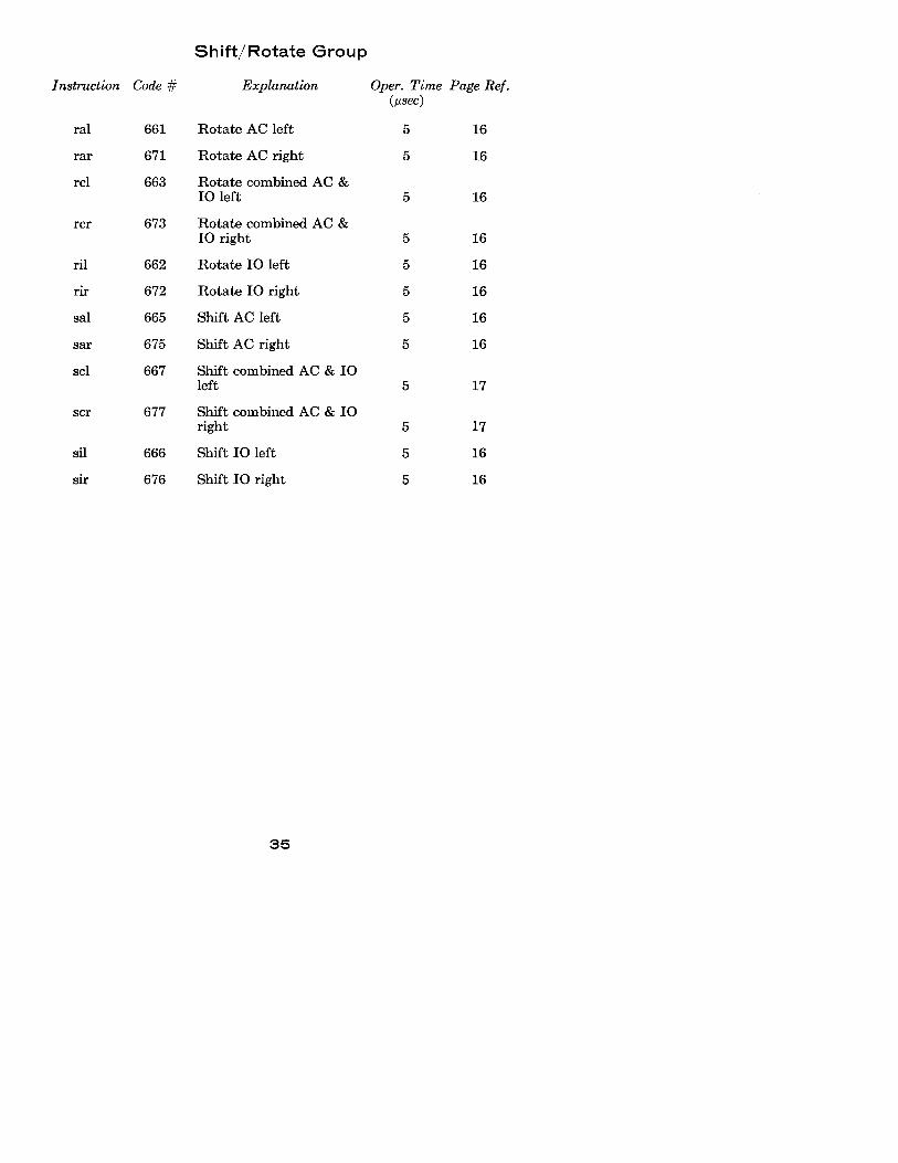
Shift/Rotate Group
Instruction Code #
ral 661
rar 671
rcl 663
rcr
ril 662
rir 672
Sal 665
sar 675
SC1 667
Sil
sir
673
677
666
676
Explanation
Rotate AC left
Rotate AC right
Rotate combined AC & IO left
Rotate combined AC & IO right
Rotate IO left
Rotate IO right
Shift AC left
Shift AC right
Shift combined AC & IO left
Shift combined AC & IO right
Shift IO left
Shift IO right
Oper. Time Page Ref. (met)
5 16
5 16
5 16
5 16
5 16
5 16
5 16
5 16
5 17
5 17
5 16
5 16
35

Code
00
02
04
06
10
12
14
16
17
20
22
24
26
30
32
34
36
NUMERICAL INSTRUCTION LIST
Instruction
*
and
ior
xor
xct
jfd
*
cal
jda
lac
lio
dac
dap
dip
dio
dzm
*
Code
40
42
44
46
50
52
54
56
60
62
64
66
70
71
72
74
76
Instruction
add
sub
idx
isP
sad
sas
mus
dis
jmp
jsp
sb
shift
law
law
iot
*
opr
* Spare code, computer will halt.
36

ALPHANUMERIC CODES
Character
a A
b B
c c
d D
e E
f F
g G
h H
i I
j J k K
1 L
mM
n N
0 0
P p
q Q
r R
8 s
t T
l.l u
v v
ww
x x
Y y
z z
FIO-DEC Code
61
62
263
64
265
266
67
70
271
241
242
43
244
45
46
247
250
51
222
23
224
25
26
227
230
31
Concise Code
61
62
63
64
65
66
67
70
71
41
42
43
44
45
46
47
50
51
22
23
24
25
26
27
30
31
37

Alphanumeric Codes (Continued)
Character
0 --f
1 I,
2 ’
3 -
4 3
5 v
6 A
7 <
8 >
9 7‘
( [
) 1 - I
- +
= > . x
I ?
Lower Case 272 72
Upper Case 274 74
Space 200 00
Backspace 75 75
Tab 236 36
(right arrow)
(double quotes)
(single quote)
(not)
(implies)
(or)
(and)
(less than)
(greater than)
(up arrow)
(non-spacing overstrike and vertical)
(minus and plus)
(non-spacing middle dot and underline)
(period and multiply)
FIO-DEC Concise Code Code
20 20
01 01
02 02
203 03
04 04
205 05
206 06
07 07
10 10
211 11
57 57
255 55
256 56
54 54
40 40
233 33
73
221
73
21
38

Alphanumeric Codes (Continued)
Character FIO-DEC Concise Code Code
Carriage Return 277 77
Tape Feed 00 00
Red * 35
Black * 34
Stop Code 13 -
Delete 100
*Used on type-out only, not on keyboard.
39
DEC TECHNICAL BULLETINS
NOTE: DEC digital circuit packages are being renamed “Modules.” As new bulletins are published, the two basic product lines will be referred to as “Laboratory Modules” instead of “Digital Test Equipment” and as “System Modules” rather than “System Building Blocks.”
DIGITAL MODULES (A-702) - short form catalog listing DEC’s complete product line.
DEC 10 Megacycle Building Blocks (A-710) -describes new 5000 Series Digital Test Equipment and 6000 Series System Building Blocks.
Expanded 100 Series DEC Digital Test Equipment (B-100) -de- scribes DEC’s 5 megacycle patchcord units.
New 3000 Series DEC Digital Test Equipment (B-3000) - describes DEC’s 500 kilocycle patchcord units.
Expanded 1000 Series DEC System Building Blocks (C-1OOOA) - describes DEC’s 5 megacycle plug-in units.
New 4000 Series DEC System Building Blocks (C-4000A)-describes DEC’s 500 kilocycle plug-in units.
DEC Basic Logic Kit (E-150) -describes a basic selection of DEC Digital Test Equipment and Accessories which can be used to perform a variety of logical operations.
DEC Programmed Data Processor (F-11A) -describes DEC’s PDP-1 high-speed, solid state, general purpose computer.
DEC Memory Tester Type 1512 (F-1512A) - describes DEC’s 1500 Series testers for coincident current core memories.
DEC Memory Tester Type 1514 (F-1514) -describes DEC’s 1500 Series testers for word address and coincident current core mem- ories.
DEC Automatic Memory Core Tester Type 2101 (F-2101)-describes DEC’s automatic tester for ferrite magnetic memory cores.
DEC Memory Exerciser Type 2201 (F-2201) -describes DEC’s exercisers for coincident current core memory systems.
Copies of the above bulletins are available on request from the DEC Sales Department, 146 Main Street, Maynard, Massachu- setts, or 8820 Sepulveda Boulevard, Los Angeles 45, California.
40