processor—consumer products i.mx 7ulp applications
TRANSCRIPT

i.MX 7ULP ApplicationsProcessor—Consumer ProductsThe i.MX 7ULP product family members are optimized for power-sensitive applications benefiting from NXP's HeterogeneousMulticore Processing (HMP) architecture. Achieving an efficientbalance between processing power and deterministic processingneeds, the i.MX 7ULP is an asymmetric processor consisting oftwo separate processing domains: an application domain and areal-time domain. The application domain is built around anARM® Cortex®-A7 processor with an ARM NEON™ SIMDengine and floating point unit (FPU) and is optimized for rich OSbased applications. The real-time domain is built around an ARMCortex-M4 processor (with FPU) optimized for lowest possibleleakage. Both domains are completely independent, withseparate power, clocking, and peripheral domains, but the busfabric of each domain is tightly integrated for efficientcommunication. The part is streamlined to minimize pin count, enabling small packages and simple systemintegration.
i.MX 7ULP features
Feature type Application processor domain Real-time processor domain
ARM Processor Cortex®-A7 Cortex®-M4
• Nominal (RUN) frequency: 500 MHz• Overdrive (HSRUN) frequency: 720
MHz• Very Low Power Run (VLPR)
frequency: 48 MHz
• Maximum frequency: 200 MHz• Very Low Power Run (VLPR)
frequency: 48 MHz
Optimized for lowest leakage current
32 KB instruction and data caches FPU
256 KB L2 cache MPU
NEON™ SIMD engine —
FPU —
On-chip memory 256 KB of RAM 256 KB of tightly coupled RAM allocated into32 KB switchable blocks
— 8 KB of OTP memory
External memoryinterfaces
16/32-bit LPDDR2/LPDDR3 interfacerunning at 380 MHz
Serial flash interface supporting x4 and x8IOs
eMMC 5.0 interface —
Security Secure boot Secure boot
Table continues on the next page...
MCIMX7U5DVP07SCMCIMX7U5DVK07SCMCIMX7U3DVK07SC
Plastic packages: BGA 14x14mm, 0.5mm pitch,and BGA 10 x 10 mm, 0.5 mm pitch
NXP Semiconductors IMX7ULPCECData Sheet: Technical Data Rev. 0, 06/2019
NXP reserves the right to change the production detail specifications as may berequired to permit improvements in the design of its products.

i.MX 7ULP features (continued)
Feature type Application processor domain Real-time processor domain
Signing and encrypt/decrypt engines(CAAM)
Encrypt/decrypt engines (LTC)
Simple tamper detection —
Serial peripherals Four I2C Fast mode plus Four I2C Fast mode plus
SD 3.0/MMC 5.0 FlexI/O
Four UARTs with flow control Four UARTs with flow control
Two LPSPI peripherals Two LPSPI peripherals
Timers Four 32-bit general-purpose timers withcapture and compare; one 64-bit timer
Four 32-bit general purpose-timers withcapture and compare; one 64-bit timer
Watchdog timer Watchdog timer
2 i.MX 7ULP Applications Processor—Consumer Products, Rev. 0, 06/2019
NXP Semiconductors

Application Domain
Real Time Domain
i.MX 7ULP
A7 Connectivity
Security
Secure JTAG
Internal Memory256K RAM
UART x 4
I2C x4
3.3V/1.8V GPIO
USB2.0 HOST(w/ HSIC)
Analog
2x 12 bit ADC
HAB – Secure Boot
Graphics
GC7000NanoULTRA
External Memory
MMC5.0/SDIO x 2
16/32-bit LPDDR2/3
PowerManager
SPI x 2
Arm Cortex -A7
NEON
Trust Zone
32KB I-cache 32KB D-cache
FPU
ETM
256KB L2 cache
Analog Comparators
External Memory
Quad SPI (OTFAD)
Timers
Watch Dog
32 bit Timer x4
System timers
Crypto / TRNG
FPUMPU
M4 ConnectivityUART x 4
I2C x4
3.3V/1.8V GPIOSPI x2
FlexIO
2x 12 -bit DAC
Internal Memory256K RAM
Timers
Watch Dog
32 bit Timer x4
System timers
Clock/Reset
Arm Cortex -- M4
DAP
DSP Extensions
USB2.0 OTG(w/ PHY)
8KB I/D - cache
MIPI DSI
Display
Secure Fuse FlexBUS
I2S x 2
eFuses / OTP
SEMA4 / Msg Unit
DMA
VIU
Camera
FlexIOGC320
Composition
SecurityuHAB – Secure Boot
Clock and Power Management System
SecureRTC
TamperDetection
Security – Batt Domain
KeyStorage
Crypto / TRNG
XRDCAccess and IPC
PLL/OSC
32K SecureMemory
Figure 1. i.MX 7ULP Block Diagram
The following table provides examples of orderable sample part numbers covered by this data sheet.
Ordering information
Part Number Options Cortex-A7
SpeedGrade
Cortex-M4
SpeedGrade
QualificationTier
JunctionTemperature
Range
Package
MCIMX7U5DVP07SC GPU-2D,GPU-3Dsupported
720 MHz 200 MHz Commercial(Consumer)
0 to +95 °C 14 mm x 14 mm, 0.5 mmpitch BGA, Package code"VP"
Table continues on the next page...
i.MX 7ULP Applications Processor—Consumer Products, Rev. 0, 06/2019 3
NXP Semiconductors

Ordering information (continued)
Part Number Options Cortex-A7
SpeedGrade
Cortex-M4
SpeedGrade
QualificationTier
JunctionTemperature
Range
Package
MCIMX7U5DVK07SC GPU-2D,GPU-3Dsupported
720 MHz 200 MHz Commercial(Consumer)
0 to +95 °C 10 mm x 10 mm, 0.5 mmpitch BGA, Package code"VK"
MCIMX7U3DVK07SC No GPU 720 MHz 200 MHz Commercial(Consumer)
0 to +95 °C 10 mm x 10 mm, 0.5 mmpitch BGA, Package code"VK"
The following figure describes the part number nomenclature so users can identify the characteristics of thespecific part number.
Figure 2. i.MX 7 Family Part Number Definition
Related Resources
Type Description
Reference Manual The i.MX 7ULP Applications Processor Reference Manual contains a comprehensive description ofthe structure and function (operation) of the SoC.
Data Sheet The Data Sheet includes electrical characteristics and signal connections.
Chip Errata The chip mask set errata provides additional or corrective information for a particular device maskset.
Package drawing Package dimensions are provided in Package information and contact assignments
4 i.MX 7ULP Applications Processor—Consumer Products, Rev. 0, 06/2019
NXP Semiconductors

i.MX 7ULP Applications Processor—Consumer Products, Rev. 0, 06/2019 5
NXP Semiconductors

Table of Contents
1 i.MX 7ULP modules list......................................................... 7
2 Clocking................................................................................ 21
2.1 Introduction.................................................................... 21
2.2 Clock distribution........................................................... 22
2.3 External clock sources...................................................23
2.4 Oscillators...................................................................... 23
2.5 Internal clock sources.................................................... 23
3 Application domain (implementing ARM Cortex-A7).............24
3.1 Memory system—application domain............................24
3.1.1 Internal memory (application domain)............... 24
3.1.2 Multi Mode DDR Controller (MMDC)................. 24
3.1.3 eMMC................................................................ 25
3.2 Peripherals—application domain................................... 25
3.2.1 Graphics processor human machine interfaces 25
3.2.2 Security—application domain............................ 25
3.2.3 Timers—application domain.............................. 27
3.2.4 Connectivity and communications—
applications domain...........................................27
4 Real-time domain (implementing ARM Cortex-M4).............. 27
4.1 Memory system—real-time domain............................... 28
4.1.1 Internal memory—real-time domain.................. 28
4.1.2 QuadSPI flash................................................... 28
4.2 Peripherals—real-time domain...................................... 28
4.2.1 Analog—real-time domain................................. 28
4.2.2 Connectivity and communications—real-time
domain...............................................................28
5 System control modules........................................................29
5.1 JTAG—system control...................................................29
5.2 JTAG device identification register................................ 29
5.3 Oscillators and PLLs......................................................29
5.3.1 System oscillator (SYS OSC)............................ 29
5.3.2 Real-Time Clock Oscillator (RTC OSC)............ 30
5.3.3 USB PLL............................................................30
5.3.4 Fixed Frequency PLL (Fixed-freq PLL)............. 30
5.3.5 Fractional-N PLL (FracN PLL)........................... 30
5.4 Power Management.......................................................30
5.4.1 Digital PMC........................................................31
5.4.2 Analog power management controller (Analog
PMC)................................................................. 31
6 System specifications............................................................31
6.1 Ratings...........................................................................31
6.1.1 Thermal handling ratings................................... 31
6.1.2 Moisture handling ratings.................................. 31
6.1.3 ESD handling ratings.........................................32
6.1.4 Absolute maximum ratings................................ 32
6.1.5 Recommended operating conditions—system.. 33
6.1.6 Fuse definition for speed grading...................... 37
6.1.7 Maximum supply currents..................................37
6.2 System clocks................................................................38
6.2.1 Clock modules................................................... 38
6.2.2 Core, platform, and system bus clock
frequency limitations..........................................41
6.2.3 Peripheral clock frequencies............................. 42
6.2.4 PLL PFD output................................................. 45
6.2.5 Audio tunable clock........................................... 46
6.3 Power sequencing—system.......................................... 47
6.3.1 Power-on sequencing........................................47
6.3.2 Power-off sequencing........................................48
6.4 Requirements for unused interfaces..............................48
6.5 Electrical Characteristics and Thermal Specifications... 49
6.5.1 AC electrical characteristics.............................. 49
6.5.2 Nonswitching electrical characteristics.............. 50
6.5.3 Switching electrical characteristics.................... 52
6.5.4 Debug and trace modules................................. 54
6.5.5 Thermal specifications.......................................57
7 Specifications—application domain...................................... 59
7.1 Peripheral operating requirements and behaviors.........59
7.1.1 DDR timing—application domain.......................59
7.1.2 Ultra-high-speed SD/SDIO/MMC host interface
(uSDHC) AC timing—application domain..........59
7.1.3 Flexbus switching specifications........................63
7.1.4 Display, Video, and Audio Interfaces.................66
7.1.5 Timer specifications—application domain......... 67
7.1.6 Connectivity and communications
specifications—application domain................... 67
8 Specifications—real-time domain..........................................76
8.1 Power sequencing—real-time domain...........................76
8.2 Peripheral operating requirements and behaviors—
real-time domain............................................................ 77
8.2.1 QuadSPI AC specifications............................... 77
8.2.2 Analog modules.................................................81
8.2.3 Timer specifications—real-time domain............ 89
8.2.4 Connectivity and communications
specifications—real-time domain.......................89
9 Package information and contact assignments.....................93
9.1 BGA, 14 x 14 mm, 0.5 mm pitch (VP suffix).................. 93
9.1.1 14 x 14 mm package case outline..................... 93
9.1.2 14 x 14 mm, 0.5 mm pitch, ball map..................95
9.1.3 14 x 14 mm power supply and functional
contact assignments..........................................97
9.2 BGA, 10 x 10 mm, 0.5 mm pitch (VK suffix).................. 105
9.2.1 10 x 10 mm package case outline..................... 105
9.2.2 10 x 10 mm, 0.5 mm pitch, ball map..................107
9.2.3 10 x 10 mm power supply and functional
contact assignments..........................................109
10 Revision History.................................................................... 117
6 i.MX 7ULP Applications Processor—Consumer Products, Rev. 0, 06/2019
NXP Semiconductors

1 i.MX 7ULP modules listThe i.MX 7ULP applications processor contains a variety of digital and analogmodules. The following table describes these modules in alphabetical order.
In the Domain column in this table:
• AD = Application Power Domain (primarily controlled by the Cortex-A7)• RT = Real-Time Power Domain (primarily controlled by the Cortex-M4)• VBAT = RTC/VBAT power domain Real-Time Domain• DGO = “always-on” DGO power domain• SYS = system-level functions that are implemented separately from the domains
listed above.
Table 1. i.MX 7ULP modules list
Block Name Block Mnemonic Subsystem PowerDomain
Brief description
AMBA NetworkInterconnectCrossbar
NIC0-1 DMA and Bus Fabrics AD The AMBA Network InterconnectCrossbar (NIC) is a highly configurableand high performance AMBA-compliantnetwork infrastructure which arbitratesbetween multiple AXI or AHB masters togrant access to internal or externalmemories or other slave devices. Itsupports connectivity between severalslave and master ports for parallelprocessing. It uses a hybrid round-robinarbitration scheme and containsfrequency converters, data widthconverters, bus protocol converter, andAXI channel buffers.
Analog PMC Analog PMC Power Management SYS The Analog PMC consists of voltage/current references, core logic supplyregulators, memory supply regulators,Back and Forward Biasing regulators,monitors and power switches, etc.There are two Analog PMC subsystemsin i.MX 7ULP, one associated with theM4 power domain and the other with theA7 power domain.
Analog-to-DigitalConverter
ADC0-1 Analog RT Analog-to-Digital Converter (ADC) is a12-bit resolution, successiveapproximation analog to digitalconverter. The ADC module supportsup to 16 single-ended external analoginputs. It outputs 12-bit, 10-bit, or 8-bitdigital signal in right-justified unsigned
Table continues on the next page...
i.MX 7ULP modules list
i.MX 7ULP Applications Processor—Consumer Products, Rev. 0, 06/2019 7
NXP Semiconductors

Table 1. i.MX 7ULP modules list (continued)
Block Name Block Mnemonic Subsystem PowerDomain
Brief description
format. The ADC can achieve 1microsecond conversion rate.
AsynchronousWakeup InterruptController
AWIC System Control RT The Asynchronous Wakeup InterruptController (AWIC) module is capable ofinterrupt detection and wake-up of aprocessor when it is in low power mode.
Bit ManipulationEngine
BME Multicore peripheralsand resource domaincontrol submodules
RT The Bit Manipulation Engine (BME)provides hardware support for atomicread-modify-write memory operations tothe peripheral address space. Thisarchitectural capability is also known as"decorated storage" as it defines amechanism for providing additionalsemantics for load and store operationsto memory-mapped peripherals beyondjust the reading and writing of datavalues to the addressed memorylocations.
Comparator CMP0-1 Analog DGO The (CMP) module provides a circuit forcomparing two analog input voltages.The comparator circuit is designed tooperate across the full range of thesupply voltage (rail to rail operation).
Cross Trigger Matrix CTM Debug RT Cross Trigger Matrix (CTM) is acomponent of the Embedded CrossTrigger (ECT), which is key in themulticore debug strategy. The CTMreceives signals from various sources(i.e. cores and peripherals) andpropagates or routes them to thedifferent debug resources of the SoC.Those debug resources can includetime stamping capability, real-timetrace, triggers and debug interrupts.
CryptographicAcceleration andAssurance
CAAM Security AD Cryptographic Acceleration andAssurance Module (CAAM) is amultifunction accelerator that supportsthe cryptographic functions common inmany security protocols. This includesAES128, AES256, DES, 3DES, SHA1,SHA224, SHA256, and a randomnumber generator with a true entropicseed. CAAM includes a DMA enginethat is descriptor based to reduceprocessor-accelerator interaction.Security feature clear keys andmemories when on-chip securitymonitor detects tampering. The SecureRAM is implemented and providessecure storage of sensitive information
Table continues on the next page...
i.MX 7ULP modules list
8 i.MX 7ULP Applications Processor—Consumer Products, Rev. 0, 06/2019
NXP Semiconductors

Table 1. i.MX 7ULP modules list (continued)
Block Name Block Mnemonic Subsystem PowerDomain
Brief description
both in on-chip RAM and in off-chip,nonvolatile memory. For details, see thei.MX 7ULP Security Reference Manual.
Cyclic RedundancyCheck
CRC Connectivity andCommunications
RT The Cyclic Redundancy Check (CRC)module is a hardware CRC generatorcircuit using 16/32-bit shift register. TheCRC module supports error detectionfor all single, double, odd, and mostmulti-bits errors, programmable initialseed value, and optional feature totranspose input data and CRC result viatranspose register.
Debug Access Port DAP Debug RT Debug Port Access (DAP) providesdebugger access to on-chip systemresources via the SWJ-DP port. TheDAP provides internal system access toA7 Debug Port, M4 Debug Port, SystemBus, JTAG controller, and SoC Controland Status. The DAP also enablessystem access to CoreSight debugsubsystem through the APBIC port.
Digital PMC Digital PMC Power Management SYS The Digital PMC module allows usersoftware to control power modes of thechip and to optimize power consumptionfor the level of functionality needed.There are two instances of Digital PMCon this device, one for each main powerdomain.
Digital-to-AnalogConverter
DAC0-1 Analog RT Digital-to-Analog Converter (DAC) is the12-bit resolution digital-to-analogconverters with programmablereference generator output. The outputof the DAC can be placed on anexternal pin or set as one of the inputsto the analog comparator or ADC. TheDAC is capable of achieving 1 msconversion rate for high-speed signalsand 2 ms conversion rate for low-speedsignals.
Direct MemoryAccess
DMA0-1 DMA and Bus Fabrics AD, RT Direct Memory Access (DMA) iscapable of performing complex datatransfers with minimal intervention froma host processor. Each DMA modulesupports 32 DMA channels. Thetransfer control descriptors for each ofthe 32 channels locate in systemmemory. DMA0 is in the real-timedomain. DMA1 is in the applicationdomain.
Table continues on the next page...
i.MX 7ULP modules list
i.MX 7ULP Applications Processor—Consumer Products, Rev. 0, 06/2019 9
NXP Semiconductors

Table 1. i.MX 7ULP modules list (continued)
Block Name Block Mnemonic Subsystem PowerDomain
Brief description
Direct MemoryAccess Multiplexer
DMAMUX0-1 DMA and Bus Fabrics AD, RT The Direct Memory Access Multiplexer(DMAMUX) module routes DMAsources, called slots, to any of thesupported DMA channels. DMAMUX0 isin the real-time domain. DMAMUX1 is inthe application domain.
Embedded TraceFIFO
ETF Debug RT The Embedded Trace FIFO (ETF)consists of a formatter, control, and thetrace RAM. It is a configuration of theTrace Memory Controller (TMC). TheETF will have a memory size of16Kbytes. The ETF and associatedmemory should be connected in thesystem such that it will retain theinformation though a warm or cold resetof the system. This is to allow for debuginformation to be retained for debuggingproblems that may arise and cause areset of the system.
Embedded TraceRouter
ETR Debug RT The ETR is a trace sink that redirectsthe trace stream onto the AXI bus toexternal storage. It can utilize a singlecontiguous region or a scatteredallocation of blocks for a circular buffer.Reading of the AXI based trace buffercan either be done directly over AXIfrom a normal bus master. The ETR is aconfiguration option of the TMC as isthe ETF.
Extended ResourceDomain Controller
XRDC Multicore Peripheralsand Resource DomainControl submodules
AD, RT The Extended Resource DomainController (XRDC) provides anintegrated, scalable architecturalframework for access control, systemmemory protection and peripheralisolation. It allows software to assignchip resources (like processor cores,non-core bus masters, memory regionsand slave peripherals) to processingdomains, to support enforcement ofrobust operational environments. TheXRDC implementation is distributedacross multiple submodules instantiatedthroughout the device.
External BusInterface
FlexBus Memories andMemory Controllers
AD The External Bus Interface (FlexBus)module provides external memoryexpansion and provides connection toexternal peripherals with a parallel,memory-mapped interface. The FlexBussupports asynchronous andsynchronous interface to external ROM,NOR flash, SRAM, PSRAM,
Table continues on the next page...
i.MX 7ULP modules list
10 i.MX 7ULP Applications Processor—Consumer Products, Rev. 0, 06/2019
NXP Semiconductors

Table 1. i.MX 7ULP modules list (continued)
Block Name Block Mnemonic Subsystem PowerDomain
Brief description
programmable logic devices and othermemory-mapped slave devices.
External WatchdogMonitor
EWM Timers RT The External Watchdog Monitor (EWM)module is designed to monitor externalcircuits, as well as the software flow.This provides a back-up mechanism tothe internal WDOG that can reset thesystem. The EWM differs from theinternal WDOG in that it does not resetthe system. The EWM, if allowed totime-out, provides an independenttrigger pin that when asserted resets orplaces an external circuit into a safemode.
Fast InternalReference Clock
FIRC Clock Sources andControl
SYS The Fast Internal Reference Clock(FIRC) module is an internal oscillatorthat can generate a reference clock inthe range from 48 MHz to 60 MHz. TheFIRC output clock is used as areference to the SCG module, and it isalso used as a clock option to most on-chip modules.
Fixed-frequency PLL Fixed-Freq PLL(PLL0)
Clock Sources andControl
SYS The Fixed-frequency PLL is the sameas the USB PLL. In addition to the mainclock output, this PLL also includes 4Phase Fractional Dividers (PFDs) thatcan generate other clock frequencies.There is one instance of the Fixed-freqPLL (PLL0) provides clocks for M4 coreand buses and peripherals in the Real-time domains.
Flexible Input/Output FLEXIO0-1 Connectivity andCommunications
AD, RT The Flexible Input/Output (FlexIO)module is capable of supporting a widerange of protocols including, but notlimited to: UART, I2C, SPI, I2S, camerainterface, display interface, PWMwaveform generation, etc. FlexIO0 is inthe real-time domain. FlexIO1 is in theapplication domain.
Fractional-N PLL Frac-N PLL(PLL1-3)
Clock Sources andControl
SYS The Fractional-N (Frac-N) PLL cangenerate an output clock of 528 MHzfrom a supported reference clock. Inaddition to the main clock output, thisPLL also includes up to 4 PhaseFractional Dividers (PFDs) that cangenerate other clock frequencies. ThisPLL also supports tunable clock foraudio applications.
GC320 CompositionProcessing Core
GPU-2D Multimedia AD Vivante GC320 is a CompositionProcessing Core (CPC) GPU. It
Table continues on the next page...
i.MX 7ULP modules list
i.MX 7ULP Applications Processor—Consumer Products, Rev. 0, 06/2019 11
NXP Semiconductors

Table 1. i.MX 7ULP modules list (continued)
Block Name Block Mnemonic Subsystem PowerDomain
Brief description
supports user interface rendering andperforms functions like blending,filtering, rotation, overlay, resizing,transparency, and other dynamiceffects.
GC7000 Nano UltraGraphic ProcessingUnit
GPU-3D Multimedia AD i.MX 7ULP integrates the VivanteGC7000 Nano Ultra Graphic ProcessingUnit (GPU-3D). supporting OpenGLES2.0/1.1, Desktop OpenGL 2.1,OpenVG1.1, and GLSL shadinglanguage support.
HardwareSemaphore
SEMA42_0 andSEMA42_1
Multicore Peripheralsand Resource DomainControl submodules
AD, RT The Hardware Semaphore (SEMA42)module provides the hardware supportneeded in multicore systems forimplementing semaphores and providea simple mechanism to achieve "lock/unlock" operations via a single writeaccess. SEMA42_0 is in the real-timedomain. SEMA42_1 is in the applicationdomain.
Input/OutputMultiplexingController
IOMUXC0-1 &IOMUXC_DDR
System Control AD, RT The Input/Output Multiplexing Controller(IOMUXC) enables the chip to shareone pad for multiple signals fromdifferent peripheral interfaces. This padsharing mechanism is done bymultiplexing the pad's input and outputsignals. The IOMUXC also controls thepads setting parameters and digital filterfunctions of the pad. In addition, theIOMUXC controls input multiplexinglogic for input signals multiplexed atmultiple locations. IOMUXC0 is in thereal-time domain. IOMUXC1 andIOMUXC_DDR are in the applicationdomain.
Internal ReferenceClock 1kHz
IRC1K Clock Sources andControl
SYS The Internal Reference Clock 1kHz(IRC1K) module is an internal oscillatorthat can generate a reference clock of1kHz. The IRC1K clock is enabled in allmodes of operation, including all lowpower modes.
Joint Test ActionGroup Controller
JTAGC Debug RT Joint Test Action Group Controller(JTAGC) provides the means to testchip functionality and connectivity whileremaining transparent to system logicwhen not in test mode. Testing isperformed via a boundary scantechnique, as defined in the IEEE1149.1-2001 standard.
Table continues on the next page...
i.MX 7ULP modules list
12 i.MX 7ULP Applications Processor—Consumer Products, Rev. 0, 06/2019
NXP Semiconductors

Table 1. i.MX 7ULP modules list (continued)
Block Name Block Mnemonic Subsystem PowerDomain
Brief description
LCD InterfaceController
LCDIF Multimedia AD The LCDIF is a general purpose displaycontroller used to drive a wide range ofdisplay devices varying in size andcapabilities. The LCDIF is used as abridge between the DSI controller andthe NIC0 crossbar.
Low-Leakage Wake-Up Unit
LLWU System Control DGO The Low-Leakage Wake-Up Unit(LLWU) module allows user to select upto 32 external pin sources and up to 8internal modules as a wakeup sourcefrom low leakage power modes.
Low Power Inter-Integrated Circuit
LPI2C0-7 Connectivity andCommunications
AD, RT The Low Power Inter-Integrated Circuit(LPI2C) module implements an efficientinterface to an I2C bus as a master. TheLPI2C can continue operating while theprocessor is in stop mode provided anappropriate peripheral clock is available.This module is designed for low CPUoverhead with DMA offloading of FIFOregister accesses. LPI2C0 - LPI2C3 arein the real-time domain. LPI2C4 -LPI2C7 are in the application domain.
Low Power PeriodicInterrupt Timer
LPIT0-1 Timers AD, RT Low Power Periodic Interrupt Timer(LPIT) is a multichannel timer modulethat can generate independent pre-trigger and trigger outputs. These timerchannels can operate individually or canbe chained together. The pre-triggerand trigger outputs can be used totrigger other modules on the device.The LPIT can also operate in low powermodes. LPIT0 is in the real-timedomain. LPIT1 is in the applicationdomain.
Low Power SerialPeripheral Interface
LPSPI0-3 Connectivity andCommunications
AD, RT The Low Power Serial PeripheralInterface (LPSPI) module implementsan efficient interface to an SPI bus as amaster and/or a slave. The LPSPI cancontinue operating while the processoris in stop mode if an appropriateperipheral clock is available. Thismodule is designed for low CPUoverhead with DMA offloading of FIFOregister accesses. LPSPI0 and LPSPI1are in the real-time domain. LPSPI2 andLPSPI3 are in the application domain.
Low-power TrustedCryptography
LTC Security RT Low-power Trusted Cryptography is anarchitecture that allows multiplecryptographic hardware acceleratorengines to be instantiated and share
Table continues on the next page...
i.MX 7ULP modules list
i.MX 7ULP Applications Processor—Consumer Products, Rev. 0, 06/2019 13
NXP Semiconductors

Table 1. i.MX 7ULP modules list (continued)
Block Name Block Mnemonic Subsystem PowerDomain
Brief description
common registers. This version of LTCsupports 128-bit AES. For details, seethe i.MX 7ULP Security ReferenceManual.
Low Power UniversalAsynchronousReceiver/Transmitter
LPUART0-7 Connectivity andCommunications
AD, RT The Low Power UniversalAsynchronous Receiver/Transmitter(LPUART) module providesasynchronous, serial communicationcapability with external devices.LPUART supports non-return-to-zero(NRZ) encoding format and IrDA-compatible infrared (low-speed) SIRformat. The LPUART can continueoperating while the processor is in stopmode if an appropriate peripheral clockis available. This module is designed forlow CPU overhead with DMA offloadingof FIFO register accesses. LPUART0 –LPUART3 are in the real-time domain.LPUART4 – LPUART7 are in theapplication domain.
Low Power Timer LPTMR0-1 Timers DGO The Low Power Timer (LPTMR) moduleis a 16-bit timer which operates as real-time interrupt or pulse accumulator. ThisLPTMR module can remain functionalwhen the chip is in low power modes,provided the reference clock to thistimer is active.
Memory-MappedCryptographicAcceleration Unit
MMCAU Security RT Memory-Mapped CryptographicAcceleration Unit (MMCAU) is anoptimized security accelerator thatsupports the cryptographic functionscommon in many security protocols.This includes DES, 3DES, AES, MD5,SHA-1, SHA-256 algorithms via simpleC calls to optimized security functions.
Messaging Unit MU Multicore Peripheralsand Resource DomainControl submodules
RT Messaging Unit (MU) is a sharedperipheral with a 32-bit IP bus interfaceand interrupt request signals to eachhost processor. The MU exposes a setof registers to each processor whichfacilitate inter-processor communicationvia 32-bit words, interrupts and flags.Interrupts may be independentlymasked by each processor to allowpolled-mode operation.
MIPI Display SerialInterface Controller
DSI Controller Multimedia AD The MIPI Display Serial InterfaceController (DSI Controller) isresponsible for serializing display datafrom the GPU. Data can come from
Table continues on the next page...
i.MX 7ULP modules list
14 i.MX 7ULP Applications Processor—Consumer Products, Rev. 0, 06/2019
NXP Semiconductors

Table 1. i.MX 7ULP modules list (continued)
Block Name Block Mnemonic Subsystem PowerDomain
Brief description
either the GPU or the processor/DMAcontroller.
MIPI Display SerialInterface PhysicalLayer
DSI PHY Multimedia AD The MIPI Display Serial InterfacePhysical Layer (DSI PHY) is a two-laneinterface that supports up to 1 Gbps ofdata on each lane. DSI PHY includes aPLL which output clock is dedicated DSIuses.
Multicore SystemMode Controller
MSMC System Control DGO Multicore System Mode Controller(MSMC) is responsible for sequencingthe system into and out of all low powerStop and Run modes. MSMC monitorsevents to trigger transitions betweenpower modes, while controlling thepower, clocks, and memories of thesystem to achieve the powerconsumption and functionality of thatmode.
Multi Mode DDRController
MMDC Memories andMemory Controllers
AD The Multi Mode DDR Controller(MMDC) is a configurable DDRcontroller that provides interface toLPDDR2 or LPDDR3 memory. TheMMDC consists of a core and PHY. Thecore is responsible for communicationwith the system through AXI interface,DDR commands generation, DDRcommand optimizations, and read/ writedata path. The PHY performs timingadjustment using special calibrationmechanisms to ensure data capturemargin at the supported clock rate.
On-The-Fly AESDecryption
OTFAD Security RT The On-The-Fly AES Decryption(OTFAD) module provides an advancedhardware implementation thatminimizes any incremental cycles oflatency introduced by the decryption inthe overall external memory accesstime. The OTFAD engine also includescomplete hardware support for astandard AES key unwrap mechanismto decrypt a key BLOB data instructioncontaining the parameters needed forup to 4 unique AES contexts.
Peripheral ClockControl
PCC0-3 Clock Sources andControl
AD, RT The Peripheral Clock Control (PCC)module is responsible for clockselection, optional division and clockgating mode for peripherals in theirrespected power domain. PCC0 andPCC1 are in the real-time domain.
Table continues on the next page...
i.MX 7ULP modules list
i.MX 7ULP Applications Processor—Consumer Products, Rev. 0, 06/2019 15
NXP Semiconductors

Table 1. i.MX 7ULP modules list (continued)
Block Name Block Mnemonic Subsystem PowerDomain
Brief description
PCC2 and PCC3 are in the applicationdomain.
Reset ModeController
RMC System Control DGO Reset Mode Controller (RMC)implements reset modes and resetfunctions of the chip.
On-Chip One-Time-ProgrammableController
OCOTP_CTRL System Control RT The On-Chip One-Time-ProgrammableController (OCOTP_CTRL) moduleprovides an interface for reading,programming and/or overridingidentification and control informationstored in on-chip fuse elements. Themodule supports electrically-programmable poly fuses. TheOCOTP_CTRL also provides a set ofvolatile software-accessible signalswhich can be used for software controlof hardware elements, not requiringnon-volatility.
Peripheral TriggerMultiplexing
TRGMUX0-1 System Control AD, RT Peripheral Trigger Multiplexing(TRGMUX) TRGMUX0 is in the real-time domain. TRGMUX1 is in theapplication domain.
Port Control PCTL_A-F System Control AD, RT The Port Control (PCTL) moduleprovides control for GPIO interruptfunction. GPIO interrupt can beconfigured independently for each pin inthe 32-bit port. There is one instance ofthe PCTL module for each port.PCTL_A and PCTL_B are in the real-time domain. PCTL_C - PCTL_F are inthe application domain.
Quad SerialPeripheral Interface
QSPI Memories andMemory Controllers
RT The Quad Serial Peripheral Interface(QSPI) module provides an interface tovarious types of serial flash memory.The QSPI interface allows one serialflash connection. It supports 1-bit, 4-bitand 8-bit SPI bus width.
Rapid General-Purpose Input andOutput
RGPIO2P0-1 System Control AD, RT The Rapid General-Purpose Input andOutput with 2 Ports (RGPIO2P) issimilar to the RGPIO module, except ithas an AHB-lite port, in addition to theIPS port, for faster access. RGPIO2P0is in the real-time domain. RGPIO2P1 isin the application domain.
Read-only memoryController
ROMCP0/1 Memories andMemory Controllers
AD, RT A ROM controller and boot ROM arepresent in for both the A7 and M4 CPUcores. ROMCP0 and a 64 kB ROM arein the real-time domain. ROMCP1 and a96 kB ROM are in the applicationdomain.
Table continues on the next page...
i.MX 7ULP modules list
16 i.MX 7ULP Applications Processor—Consumer Products, Rev. 0, 06/2019
NXP Semiconductors

Table 1. i.MX 7ULP modules list (continued)
Block Name Block Mnemonic Subsystem PowerDomain
Brief description
Real Time ClockOscillator
RTC OSC Clock Sources andControl
VBAT The Real Time Clock Oscillator (RTCOSC) module provides the clock sourcefor the Real-Time Clock module. TheRTC OSC module, in conjunction withan external crystal, generates a 32.678kHz reference clock for the RTC.
Single Wire Output SWO Debug RT Single Wire Output (SWO) is a tracedata drain that acts as bridge betweenthe on-chip trace data to a data streamthat is captured by the Trace PortAnalyzer. It is a TPIU-like device thatsupports a limited subset of the fullTPIU functionality for a simple debugsolution.
Secure JTAGController
SJC Debug RT The Secure JTAG Controller (SJC) is anauthenticated debug module thatimplements a challenge/responsemechanism using a standardcryptographic algorithm. This allowspost production silicon debug withoutcompromising security requirements.The SJC is connected in parallel withthe JTAGC module, but it is only usedfor authenticated debug.
Secure Non-VolatileStorage
SNVS Security VBAT The Secure Non-Volatile Storage(SNVS) module is designed to safelyhold security-related data such ascryptographic key, time counter,monotonic counter, and generalpurpose security information. A part ofthe SNVS module belongs to the VBATdomain that has its own dedicatedpower supply which is always on. Thisenables SNVS to keep this data validand continue to increment the timecounter when the power goes down inthe rest of the SoC. SNVS includes theReal-Time Clock (RTC) module, whichprovides 64-bit monotonic counter withroll-over protection, 32-bit secondscounter with roll-over protection and 32-bit alarm.
Slow InternalReference Clock
SIRC Clock Sources andControl
SYS The Slow Internal Reference Clock(SIRC) module is an internal oscillatorthat can generate a reference clock of16 MHz. The SIRC output clock is usedas a reference to the SCG module, andit is also used as a clock option to moston-chip modules.
Table continues on the next page...
i.MX 7ULP modules list
i.MX 7ULP Applications Processor—Consumer Products, Rev. 0, 06/2019 17
NXP Semiconductors

Table 1. i.MX 7ULP modules list (continued)
Block Name Block Mnemonic Subsystem PowerDomain
Brief description
Synchronous AudioInterface
SAI0-1 Multimedia RT The Synchronous Audio Interface (SAI)module implements full-duplex serialinterfaces with frame synchronizationsuch as I2S, AC97, and CODEC/DSPinterfaces.
System ClockGeneration
SCG0-1 Clock Sources andControl
AD, RT The System Clock Generation (SCG)module is responsible for clockgeneration and distribution across thisdevice. Functions performed by theSCG include: clock reference selection,generation of clock used to deriveprocessor, system, peripheral bus andexternal memory interface clocks;source selection for peripheral clocks;and, control of power saving clockgating mode. SCG0 is in the real-timedomain. SCG1 is in the applicationdomain.
System IntegrationModule
SIM System Control AD, RT The System Integration Module (SIM)provides system control and chipconfiguration registers. The SIMincludes the TSTMR module.
System Oscillator SYS OSC Clock Sources andControl
SYS The System Oscillator (SYS OSC)module is a crystal oscillator. The SYSOSC, in conjunction with an externalcrystal or resonator, generates areference clock for this device. It alsooptionally supports an external inputclock provided to EXTAL signal directly.
Tightly-CoupledMemory
TCM Memories andMemory Controllers
RT Tightly Coupled Memory (TCM) RAM.This RAM is tightly integrated to the M4processor. M4 accesses this memorywith zero wait-state. There is abackdoor port that allows M4 DMA andother bus masters in the SoC to accessthis memory.
Timer/Pulse WidthModulation
LPTPM0-7 Timers AD, RT The Timer/Pulse Width ModulationModule (TPM) is a multichannel timermodule that supports input capture,output compare, and the generation ofPWM signals. The counter, compareand capture registers are clocked by anasynchronous clock that can remainenabled in low power modes. LPTPM0– LPTPM3 are in the real-time domain.LPTPM4 – LPTPM7 are in theapplication domain.
TimeStampComponents
TimeStampComponents
Debug RT The timestamp components generateand distribute a consistent timestamp
Table continues on the next page...
i.MX 7ULP modules list
18 i.MX 7ULP Applications Processor—Consumer Products, Rev. 0, 06/2019
NXP Semiconductors

Table 1. i.MX 7ULP modules list (continued)
Block Name Block Mnemonic Subsystem PowerDomain
Brief description
value for multiple processors and otherblocks in a SoC.
Timestamp timer TSTMR Timers AD, RT The TSTMR module is a free runningincrementing counter that starts runningafter system reset de-assertion and canbe read at any time by the software fordetermining the software ticks. TheTSTMR is a 64-bit clock cycle counter.It runs off the 1 MHz clock and resetson every system reset. The counter onlystops when the clock to the TSTMR isdisabled.
Trace Funnel FUNL Debug RT The Trace Funnel (FUNL) is used whenthere is more than one trace source.The Trace Funnel combines multipletrace streams onto a single ATB bus.The Trace Funnel includes an arbiterthat determines the priority of the ATBinputs.
Trace Port InterfaceUnit
TPIU Debug RT Trace Port Interface Unit (TPIU) acts asa bridge between on-chip trace data, IDdistinguishable, and a TPA. It receivesATB trace data and sends it off chip viaARM’s standard trace interface. TheTPIU includes ATB interface, APBinterface, Formatter, AsynchronousFIFO, Register bank, Trace outserializer, and a pattern generator.
Trace Replicator Replicator Debug RT The Trace Replicator (Replicator)enables two trace sinks (TPIU andTMC) to be wired together and receiveATB trace data from the same tracesource. It takes incoming data from asingle source and replicates it to twomaster ports.
True RandomNumber Generator
TRNG Security RT The True Random Number Generator(TRNG) module is to generate highquality, cryptographically secure,random data. The TRNG module iscapable of generating its own entropyusing an integrated ring oscillator. Inaddition, the module’s NIST certifiablePseudo-Random Number Generator(PRNG) provides acceleratedprocessing of pseudo-random data.
ultra Secured DigitalHost Controller
uSDHC0/1 Memories andMemory Controllers
AD The ultra Secured Digital HostController (uSDHC) provides theinterface between the host system andSD, SDIO or eMMC cards. The uSDHCacts as a bridge, passing host bus
Table continues on the next page...
i.MX 7ULP modules list
i.MX 7ULP Applications Processor—Consumer Products, Rev. 0, 06/2019 19
NXP Semiconductors

Table 1. i.MX 7ULP modules list (continued)
Block Name Block Mnemonic Subsystem PowerDomain
Brief description
transactions to the cards by sendingcommands and performing dataaccesses to/from the cards or devices.It handles SD, SDIO and eMMCprotocol at transmission level.
Universal Serial BusHigh-Speed InterChip Physical Layer
HSIC-PHY Connectivity andCommunications
AD USB High-Speed Inter Chip PhysicalLayer (HSIC-PHY) is a complete digitalIP designed to implement USB 2.0HSIC connectivity interface.
Universal Serial BusOn-The-Go
USB-OTG Connectivity andCommunications
AD The Universal System Bus On-The-Go(USB-OTG) module is a USB 2.0-compliant implementation. The registersand data structures of this USBcontroller are based on the EnhancedHost Controller Interface Specificationfor Universal Serial Bus (EHCI). Thismodule can act as a host, a device oran On-The-Go negotiable host/deviceon the USB bus.
Universal Serial BusPhase Locked Loop
USB PLL Clock Sources andControl
AD USB Phase Locked Loop (USB PLL) isembedded in the USB transceiver block.This PLL allows an exact 480 MHz to begenerated from a supported referenceclock of 24 MHz. The output of this PLLis primarily used for PLL operation. TheUSB PLL clock is also made availableas a clock source for other peripheralsin the SoC.
Universal Serial BusPhysical Layer
USB-PHY Connectivity andCommunications
AD The Universal System Bus PhysicalLayer (USB-PHY) implements USBphysical layer connecting to USB host/device systems at low-speed, full-speed, and high-speed. USB-PHYprovides a standard UTMI interface forconnection to the USB-OTG controller.
Video Input Unit VIU Multimedia AD The Video Input Unit (VIU) provides aparallel interface for digital video. TheVIU accepts various types of digitalvideo input on its parallel interface,decodes it and optionally performsprocesses such as down-scaling,horizontal up-scaling, brightness andcontrast adjustment, pixel formatconversion, deinterlacing and horizontalmirroring. The resultant video stream isthen stored to system memory forsubsequent post-processing anddisplay.
Wakeup Unit WKPU System Control AD Wakeup Unit (WKPU) module iscapable of interrupt detection and wake-
Table continues on the next page...
i.MX 7ULP modules list
20 i.MX 7ULP Applications Processor—Consumer Products, Rev. 0, 06/2019
NXP Semiconductors

Table 1. i.MX 7ULP modules list (continued)
Block Name Block Mnemonic Subsystem PowerDomain
Brief description
up of the Cortex-A processor when it isin low power mode.
Watchdog Timer WDOG0-2 Timers AD, RT The Watchdog Timer (WDOG) modulekeeps a watch on the systemfunctioning and resets it in case of itsfailure. Reasons for failure include run-away software code and the stoppageof the system clock that in a safetycritical system can lead to seriousconsequences. In such cases, theWDOG brings the system into a safestate of operation. The WDOG monitorsthe operation of the system byexpecting periodic communication fromthe software, generally known asservicing or refreshing the WDOG. Ifthis periodic refreshing does not occur,the WDOG resets the system. WDOG0is in the real-time domain. WDOG1 andWDOG2 are in the application domain.
XRDC Manager MGR Multicore Peripheralsand Resource DomainControl submodules
RT The XRDC Manager (MGR) submodulecoordinates all programming modelreads and writes.
XRDC MasterDomain AssignmentController
MDAC Multicore Peripheralsand Resource DomainControl submodules
AD, RT The XRDC Master Domain AssignmentController (MDAC) submodule handlesresource assignments and generation ofthe domain identifiers.
XRDC MemoryRegion Controller
MRC Multicore Peripheralsand Resource DomainControl submodules
AD, RT The XRDC Memory Region Controller(MRC) submodule implements theaccess controls for slave memoriesbased on the pre-programmed regiondescriptor registers.
XRDC PeripheralAccess Controller
PAC Multicore Peripheralsand Resource DomainControl submodules
AD, RT The XRDC Peripheral Access Controller(PAC) implements the access controlsfor slave peripherals based on the pre-programmed domain access controlregisters.
2 Clocking
Clocking
i.MX 7ULP Applications Processor—Consumer Products, Rev. 0, 06/2019 21
NXP Semiconductors
2.1 Introduction
This section details the clock sources, distribution and management within the i.MX7ULP. These functions are under joint control of the System Clock Generation (SCG)modules, Peripheral Clock Control (PCC) modules, and Core Mode Controller (CMC)blocks.
NOTEReferences in this chapter to “Core 0” or “Processor A”correspond to the Cortex M4 core. References in this chapterto “Core 1” or “Processor B” correspond to the Cortex A7core.
The clocking scheme provides clear separation between M4 domain and A7 domain.Except for a few clock sources shared between two domains, such as the SystemOscillator clock, the Slow IRC (SIRC), and the Fast IRC clock (FIRC), clock sourcesand clock management are separated and contained within each domain.
M4 clock management consists of SCG0, PCC0, PCC1, and CMC0 modules.
A7 clock management consists of SCG1, PCC2, PCC3, and CMC1 modules.
2.2 Clock distributionThe SCG modules generate and distribute clocks on the device. SCG functions include:
• clock reference selection• generation of clock used to derive processor, system, peripheral bus and external
memory interface clocks• source selection for peripheral clocks• control of power-saving clock-gating mode
PCC modules control clock selection, optional division and clock gating mode forperipherals.
NOTE• To bypass system oscillator and directly apply clock from
pin, SCG_SOSCCFG[EREFS] should be set to 0. Thedirect clock should be applied on the EXTAL pin.
• For using oscillator reference,SCG_SOSCCSR[SOSCEN] andSCG_SOSCCFG[EREFS] should both be set to 1.
Clocking
22 i.MX 7ULP Applications Processor—Consumer Products, Rev. 0, 06/2019
NXP Semiconductors

2.3 External clock sourcesIn normal functional mode, this device operates off two primary external referenceclocks: System oscillator clock (SOSC) and RTC oscillator clock (ROSC):
• System oscillator clock is a high frequency reference clock with a frequency inthe range of 16 MHz to 32 MHz. This clock is used as a reference clock to the on-chip PLLs which generate all the required high frequency clocks.
• RTC oscillator clock is the 32.768 kHz constant frequency, real-time clock.
2.4 Oscillators
The system oscillator, in conjunction with an external crystal or resonator, generates areference clock for the device. The system oscillator module supports 16-32 MHzcrystals or resonators. It also provides the option for an external input clock toEXTAL signal directly.
The RTC oscillator is in the VBAT domain. The RTC oscillator module, inconjunction with an external crystal, generates a 32.768 kHz real-time reference clockfor the RTC and will always be enabled and supplying clock to SRTC. This is thedefault clock source.
2.5 Internal clock sourcesThis device is capable of generating these internal reference clocks:
• The FIRC is the fast IRC clock with nominal frequency in the range from 48 to 60MHz. In addition, the FIRC provides a clock selection option for peripherals.
• The SIRC is the slow IRC clock with nominal frequency of 16 MHz. The SIRCprovides a clock selection option for peripherals.
• The IRC1K generates 1 kHz clock that is enabled in all modes of operation,including all low power modes.
• The RTC OSC has the capability to provide nominal 32 kHz (not recommendedfor accurate clock and normal operation) IRC in absence of the external OSCreference clock if the VBAT domain is enabled.
NOTEThe internal oscillator is automatically multiplexed in theclocking system when the system detects a loss of clock.The internal oscillator will provide clocks to the same on-
Clocking
i.MX 7ULP Applications Processor—Consumer Products, Rev. 0, 06/2019 23
NXP Semiconductors

chip modules as the external 32 kHz oscillator. The internaloscillator is not precise relative to a crystal. While it willprovide a clock to the system, it generally will not be preciseenough for long-term time keeping. The internal oscillator isanticipated to be useful for quicker start-up times andtampering prevention, but should not be used as the exclusivesource for the 32 kHz clocks. An external 32 kHz clocksource must be used for production systems.
3 Application domain (implementing ARM Cortex-A7)The application domain is built around an ARM Cortex-A7 processor optimized to runnominally at 500 MHz, supported by a 32 KB L1 instruction and data cache, a large L2cache, and an LPDDR2/LPDDR3 memory interface. The Cortex-A7 processor is ahigh-performance low-power processor that implements the ARMv7-A architecture. Ituses the generic interrupt controller (GIC), generic 64-bit OS timer, FPU and the ARMNEON SIMD engine. Additionally, all the optional debug features are included.
3.1 Memory system—application domain
3.1.1 Internal memory (application domain)
3.1.2 Multi Mode DDR Controller (MMDC)
The Multi Mode DDR Controller is a dedicated interface to LPDDR2/LPDDR3SDRAM.
The i.MX 7ULP MMDC is compatible with the following JEDEC-compliant memorytypes:
• LPDDR2 SDRAM compliant to JESD209-2F LPDDR2 JEDEC standard releasedJune, 2013
• LPDDR3 SDRAM compliant to JESD209-3C JEDEC standard released August,2015
Application domain (implementing ARM Cortex-A7)
24 i.MX 7ULP Applications Processor—Consumer Products, Rev. 0, 06/2019
NXP Semiconductors

MMDC operation with the standards stated above is contingent upon the board DDRdesign adherence to the DDR design and layout requirements stated in the HardwareDevelopment Guide for the i.MX 7ULP Applications Processor (IMX7ULPHDG).
The table below shows the supported LPDDR2/LPDDR3 configurations:
Table 2. i.MX 7ULP supported LPDDR2/LPDDR3 configurations
Parameter LPDDR2 LPDDR3
Clock frequency up to 380 MHz
Bus width x16/x32
Channel Single
Chip select Up to two
3.1.3 eMMC
eMMC is a managed NAND device.
See Ultra-high-speed SD/SDIO/MMC host interface (uSDHC) AC timing—application domain.
3.2 Peripherals—application domain
3.2.1 Graphics processor human machine interfacesThe i.MX 7ULP Application Domain implements the following graphics processorhuman machine interfaces:
• 3D graphics processing unit (GPU-3D)• 2D graphics processing unit (GPU-2D)• MIPI Display Serial Interface Controller (MIPI DSI)• Video Interface Unit (VIU)
See the i.MX 7ULP modules list for more details.
3.2.2 Security—application domain
Application domain (implementing ARM Cortex-A7)
i.MX 7ULP Applications Processor—Consumer Products, Rev. 0, 06/2019 25
NXP Semiconductors

3.2.2.1 True Random Number Generator (TRNG)
The TRNG module is used to generate high quality, cryptographically secure, randomdata. The TRNG module is capable of generating its own entropy using an integratedring oscillator. In addition, the module’s Pseudo-Random Number Generator (PRNG)provides accelerated processing of pseudo-random data.
3.2.2.2 Real-Time Clock (RTC)
The RTC module provides 64-bit monotonic counter with roll-over protection, 32-bitseconds counter with roll-over protection and 32-bit alarm. This timer module isextremely low power that allows it to operate on a backup power supply when the mainpower supply is cut off. The RTC remains functional in all low power modes and cangenerate an interrupt to exit any low power mode.
3.2.2.3 High Assurance Boot (HAB)
The High Assurance Boot (HAB) component of the ROM protects against the potentialthreat of attackers modifying areas of code or data in programmable memory to make itbehave in an incorrect manner. The HAB also prevents attempts to gain access tofeatures which should not be available.
The integration of the HAB feature with the ROM code ensures that the chip does notenter an operational state if the existing hardware security blocks have detected acondition that may be a security threat or areas of memory deemed to be important havebeen modified. The HAB uses RSA digital signatures to enforce these policies.
SN
VS
CAAM
Core Processor HA
B
RO
M
Flash
RAM
Figure 3. Secure Boot Components
Application domain (implementing ARM Cortex-A7)
26 i.MX 7ULP Applications Processor—Consumer Products, Rev. 0, 06/2019
NXP Semiconductors

NOTENXP provides a reference Code Signing Tool (CST) for keygeneration, certificate generation and code signing for usewith the HAB library. The CST can be found by searchingfor "IMX_CST_TOOL" at http://www.nxp.com.
NOTEFor further details on making use of the secure boot featureusing HAB, contact your local NXP representative.
3.2.3 Timers—application domainThe i.MX 7ULP Application Domain implements the following timers:
• Low Power Periodic Interrupt Timer (LPIT)• Timer/PWM Module (LPTPM)• Low Power Timer (LPTMR)• External Watchdog Monitor (EWM)• Time stamp timer module (TSTMR)• WDOG (Watchdog Timer)
See i.MX 7ULP modules list for more details.
3.2.4 Connectivity and communications—applications domainThe i.MX 7ULP Application Domain implements the following connectivity andcommunications peripherals:
• Secure Digital (SD) Interface via the uSDHC• Low Power Universal Asynchronous Receiver/Transmitter (LPUART)• Low Power Inter-Integrated Circuit (LPI2C)• Low Power Serial Peripheral Interface (LPSPI)• Universal System Bus On-The-Go (USB-OTG)• USB High-Speed Inter-Chip Physical Layer (HSIC-PHY)
See i.MX 7ULP modules list for more details.
4 Real-time domain (implementing ARM Cortex-M4)The real-time domain is built around an ARM Cortex-M4 processor that contains afloating-point unit and is optimized for lowest possible leakage.
Real-time domain (implementing ARM Cortex-M4)
i.MX 7ULP Applications Processor—Consumer Products, Rev. 0, 06/2019 27
NXP Semiconductors

4.1 Memory system—real-time domain
4.1.1 Internal memory—real-time domain
The real-time domain contains 256 kB of SRAM organized in sub-blocks of 32 kBeach. Each sub-block can be power-gated under software control to optimize powerconsumption.
4.1.2 QuadSPI flash
The Quad Serial Peripheral Interface (QSPI) module provides an interface to varioustypes of serial flash memory. It allows one serial flash connection and supports 1-bit, 4-bit and 8-bit SPI bus width.
4.2 Peripherals—real-time domain
4.2.1 Analog—real-time domainThe i.MX 7ULP Real-Time Domain implements the following analog peripherals:
• 12-bit Analog to Digital Converter• 12-bit Digital to Analog Converter• Comparators
See i.MX 7ULP modules list for more details.
4.2.2 Connectivity and communications—real-time domainThe i.MX 7ULP Real-Time Domain implements the following connectivity andcommunications peripherals:
• Low Power Universal Asynchronous Receiver/Transmitter (LPUART)• Low Power Inter-Integrated Circuit (LPI2C)• Low Power Serial Peripheral Interface (LPSPI)• Rapid General-Purpose Input and Output with 2 Ports (RGPIO2P)• Flexible Input/Output (FlexIO)
See the i.MX 7ULP modules list for more details.
Real-time domain (implementing ARM Cortex-M4)
28 i.MX 7ULP Applications Processor—Consumer Products, Rev. 0, 06/2019
NXP Semiconductors

5 System control modules
5.1 JTAG—system control
Joint Test Action Group Controller (JTAGC) provides the means to test chipfunctionality and connectivity while remaining transparent to system logic when notin test mode. Testing is performed via a boundary scan technique, as defined in theIEEE 1149.1-2001 standard.
5.2 JTAG device identification register
The device identification register (JTAG ID) allows the revision number and partnumber to be read through the TAP. See the device identification register section ofthe i.MX 7ULP Applications Processor Reference Manual for details. This tableshows the Part Identification Number (PIN) and the Part Revision Number (PRN) foreach i.MX 7ULP silicon revision.
Table 3. JTAG device identification register information
Silicon Revision Part Identification Number (PIN) Part Revision Number (PRN)
A0 10'b0011100001 4’b0000
B0 10'b0011100001 4’b0001
B1 10'b0011100001 4’b0010
The contents of the JTAD ID register are also mirrored in a SIM register calledJTAG_ID_REG (address 0x410A_308C).
5.3 Oscillators and PLLs
5.3.1 System oscillator (SYS OSC)
The system oscillator (SYS OSC) is a crystal oscillator. The SYS OSC, in conjunctionwith an external crystal or resonator, generates a reference clock for this chip. It alsoprovides the option for an external input clock to EXTAL signal directly.
System control modules
i.MX 7ULP Applications Processor—Consumer Products, Rev. 0, 06/2019 29
NXP Semiconductors

5.3.2 Real-Time Clock Oscillator (RTC OSC)
The RTC OSC module provides the clock source for the Real-Time Clock module. TheRTC OSC module, in conjunction with an external crystal, generates a 32.678 kHzreference clock for the RTC.
5.3.3 USB PLL
The USB PLL is embedded in the USB transceiver block. This PLL allows an exact 480MHz to be generated from a supported reference clock of 24 MHz. The output of thisPLL is primarily used for USB operations. The USB PLL clock is also made availableas a clock source for other peripherals in the SoC.
5.3.4 Fixed Frequency PLL (Fixed-freq PLL)
In addition to the main clock output, this PLL also includes 4 Phase Fractional Dividers(PFDs) that can generate other clock frequencies. There is one instance of the Fixed-freq PLL (PLL0), which provides clocks for the M4 core, buses, and peripherals in thereal-time domain.
5.3.5 Fractional-N PLL (FracN PLL)
The Fractional-N (Frac-N) PLL can generate an output clock 528 MHz from asupported reference clock. In addition to the main clock output, this PLL also includesup to four Phase Fractional Dividers (PFDs) that can generate other clock frequencies.This PLL also supports a tunable clock for audio applications.
5.4 Power ManagementThe i.MX 7ULP implements multiple options minimizing application powerconsumption:
• On-chip power management including regulators, drivers and switches for flexiblepower supplies, efficient power consumption and short wake up time
• Multiple power domains and ultra-low power modes allow flexible power saving• Voltage and frequency scaling in dynamic operating modes
System control modules
30 i.MX 7ULP Applications Processor—Consumer Products, Rev. 0, 06/2019
NXP Semiconductors

• Software-controlled clock gating for cores and peripherals• Dynamic Process Monitor (DPM)
5.4.1 Digital PMC
The digital PMC module allows user software to control power modes and of the chipand to optimize power consumption for the level of functionality needed. There aretwo instances of digital PMC on this chip, one for each main power domain.
5.4.2 Analog power management controller (Analog PMC)
The Analog PMC consists of voltage/current references, core logic supply regulators,memory supply regulators, back and forward biasing regulators, monitors and powerswitches, etc. There are two Analog PMC subsystems, one associated with the M4power domain and the other with the A7 power domain.
6 System specifications
6.1 Ratings
6.1.1 Thermal handling ratings
Symbol Description Min. Max. Unit Notes
TSTG Storage temperature -55 150 °C 1
TSDR Solder temperature, lead-free — 260 °C 2
1. Determined according to JEDEC Standard JESD22-A103, High Temperature Storage Life.2. Determined according to IPC/JEDEC Standard J-STD-020, Moisture/Reflow Sensitivity Classification for Nonhermetic
Solid State Surface Mount Devices.
System specifications
i.MX 7ULP Applications Processor—Consumer Products, Rev. 0, 06/2019 31
NXP Semiconductors

6.1.2 Moisture handling ratings
Symbol Description Min. Max. Unit Notes
MSL Moisture sensitivity level — 3 — 1
1. Determined according to IPC/JEDEC Standard J-STD-020, Moisture/Reflow Sensitivity Classification for NonhermeticSolid State Surface Mount Devices.
6.1.3 ESD handling ratings
Symbol Description Min. Max. Unit Notes
VHBM Electrostatic discharge voltage, human body model -1000 +1000 V 1
VCDM Electrostatic discharge voltage, charged-devicemodel
-250 +250 V 2
1. Determined according to JEDEC Standard JESD22-A114, Electrostatic Discharge (ESD) Sensitivity Testing HumanBody Model (HBM).
2. Determined according to JEDEC Standard JESD22-C101, Field-Induced Charged-Device Model Test Method forElectrostatic-Discharge-Withstand Thresholds of Microelectronic Components.
6.1.4 Absolute maximum ratings
CAUTIONStresses beyond those listed under this table may causepermanent damage to the device. These are stress ratings only.Functional operation of the device at these or any otherconditions beyond those indicated under “recommendedoperating conditions” is not implied. Exposure to absolute-maximum-rated conditions for extended periods may affectdevice reliability.
Table 4. Absolute maximum ratings
Parameter Description Symbol Min Max Unit
SNVS domain LDO supply input VDD_VBAT42 -0.3 4.25 V
M4/A7 PMC and PMC IO supply input VDD_PMC18 -0.3 1.98 V
1.8V IO supply reference and A7 supply reference input VDD18_IOREF -0.3 1.98 V
M4 domain LDO and internal memory LDO supply input VDD_PMC18_DIG0 -0.3 1.98 V
M4 domain core and logic supply input VDD_DIG0 -0.3 1.155 V
A7 domain core and logic supply inputs VDD_PMC12_DIG1 -0.3 1.65 V
VDD_PMC11_DIG1_CAP1 -0.3 1.155 V
Table continues on the next page...
System specifications
32 i.MX 7ULP Applications Processor—Consumer Products, Rev. 0, 06/2019
NXP Semiconductors

Table 4. Absolute maximum ratings (continued)
Parameter Description Symbol Min Max Unit
VDD_DIG1 -0.3 1.155 V
GPIO Port A supply input VDD_PTA -0.3 3.96 V
GPIO Port B supply input VDD_PTB -0.3 1.98 V
GPIO Port C supply input VDD_PTC -0.3 3.96 V
GPIO Port D supply input VDD_PTD -0.3 3.96 V
GPIO Port E supply input VDD_PTE -0.3 3.96 V
GPIO Port F supply input VDD_PTF -0.3 3.96 V
HSIC supply input VDD_HSIC -0.3 1.98 V
HSIC 1.8V pre-driver supply input VDD18_HSIC -0.3 1.98 V
DDR I/O supply input VDD_DDR -0.3 1.98 V
DDR 1.8V pre-driver supply input VDD18_DDR -0.3 1.98 V
MIPI DSI 1.1V supply input VDD_DSI11 -0.3 1.155 V
MIPI DSI 1.8V supply input VDD_DSI18 -0.3 1.98 V
USB PHY 3.3V supply input VDD_USB33 -0.3 3.6 V
USB PHY 1.8V supply input VDD_USB18 -0.3 1.98 V
USB0 VBUS detection USB0_VBUS -0.3 5.6 V
PLL analog supply input VDD_PLL18 -0.3 1.98 V
ADC high reference supply input VREFH_ANA18 -0.3 1.98 V
ADC analog and IO 1.8V supply input VDD_ANA18 -0.3 1.98 V
ADC analog and IO 3.3V supply input VDD_ANA33 -0.3 3.96 V
1. When used as an input in LDO Bypass Mode
6.1.5 Recommended operating conditions—system
NOTEAll supply inputs shown represent the voltage at the packageball.
Table 5. Recommended operating conditions
Symbol Description Conditions Min Typ Max Units
SNVS (Always On) Domain Supply Voltage Requirements
VDD_VBAT42 SNVS domain LDO supplyinput
— 2.4 3.0 4.2 V
VDD_VBAT18_CAP SNVS domain LDO output — — 1.8 — V
Real Time Domain (M4 domain) Supply Voltage Requirements (LDO-Enabled Mode only supported)
VDD_PMC181 M4/A7 PMC and PMC IOsupply input
— 1.71 1.8 1.89 V
Table continues on the next page...
System specifications
i.MX 7ULP Applications Processor—Consumer Products, Rev. 0, 06/2019 33
NXP Semiconductors

Table 5. Recommended operating conditions (continued)
Symbol Description Conditions Min Typ Max Units
VDD18_IOREF1 1.8V IO supply referenceand A7 supply referenceinput
— 1.71 1.8 1.89 V
VDD_PMC18_DIG02 M4 domain LDO and internalmemory LDO supply input
HSRUN mode notsupported
1.14 1.2 1.89 V
HSRUN modesupported
1.2 1.8 1.89 V
VDD_PMC11_DIG0_CAP3, 4 M4 domain LDO supplyoutput
— 0.65 — 1.1 V
Real Time Domain (M4 domain) PMC 0 Register Configuration Requirements
PMC0_HSRUN[COREREGVL]
PMC0 HSRUN mode LDOconfiguration requirements
HSRUN modeFBB=0.3 V
— 101010b(1.05 V)
— —
PMC0_RUN [COREREGVL] PMC0 RUN mode LDOconfiguration requirements
RUN mode No bias — 011100b(0.90 V)
— —
PMC0_VLPR[COREREGVL]
PMC0 VLPR mode LDOconfiguration requirements
VLPR mode — 011100b(0.90 V)
— —
PMC0_STOP[COREREGVL]
PMC0 STOP mode LDOconfiguration requirements
STOP mode — 011100b(0.90 V)
— —
PMC0_VLPS[COREREGVL]
PMC0 VLPS mode LDOconfiguration requirements
VLPS mode — 011100b(0.90 V)
— —
PMC0_LLS [COREREGVL] PMC0 LLS mode LDOconfiguration requirements
LLS mode — 001101b(0.73V)
— —
RDIG0 External board routingimpedance fromVDD_PMC11_DIG0_CAP toVDD_DIG0
— — — 50 mΩ
Application Domain (A7 domain) supply voltage requirements for LDO Bypass mode5
VDD_PMC12_DIG1
VDD_PMC11_DIG1_CAP
VDD_DIG1
A7 domain core and logicsupply inputs
HSRUN mode; FBB= 0.3V6
1.09 — 1.15 V
RUN mode; No Bias 1.00 — 1.15 V
VLPR mode 0.87 — 1.15 V
WAIT mode 1.00 — 1.15 V
STOP mode (CA7halted andperipherals runningat full rated speed)
1.00 — 1.15 V
STOP mode (CA7halted andperipherals runningat VLPR speeds)
0.87 — 1.15 V
VLPS mode7 0.73 — 1.15 V
LLS Mode 0.73 — 1.15 V
VLLS Mode8 0.73 — 1.15 V
Application Domain (A7 domain) PMC1 register configuration requirements for LDO Enabled mode9
Table continues on the next page...
System specifications
34 i.MX 7ULP Applications Processor—Consumer Products, Rev. 0, 06/2019
NXP Semiconductors

Table 5. Recommended operating conditions (continued)
Symbol Description Conditions Min Typ Max Units
VDD_PMC12_DIG1 A7 domain LDO and internalmemory LDO supply input
— 1.14 1.2 1.32 V
VDD_PMC11_DIG1_CAP10 A7 domain LDO supplyoutput
— 0.65 — 1.15 V
PMC1_RUN[LDOVL] PMC1 RUN mode LDOconfiguration requirements
RUN mode; No Bias — 100011b(0.95V)
— V
PMC1_VLPR[LDOVL] PMC1 VLPR mode LDOconfiguration requirements
VLPR mode — 011110b(0.90V)
— V
PMC1_STOP[LDOVL] PMC1 STOP mode LDOconfiguration requirements
STOP mode (CA7halted andperipherals runningat full rated speed)
— 100011b(0.95V)
— V
PMC1_STOP[LDOVL] PMC1 STOP mode LDOconfiguration requirements
STOP mode (CA7halted andperipherals runningat VLPR speeds)
— 011110b(0.90V)
— V
PMC1_VLPS[LDOVL] PMC1 VLPS mode LDOconfiguration requirements
VLPS mode — 011110b(0.90V)
— V
PMC1_LLS[LDOVL] PMC1 LLS mode LDOconfiguration requirements
LLS Mode — 001011b(0.71V)
— V
RDIG1 External board routingimpedance fromVDD_PMC11_DIG1_CAP toVDD_DIG1
— — — 50 mΩ
GPIO Supplies11
VDD_PTA12, 13 GPIO Port A supply input — 1.71 1.8 or 3.3 3.6 V
VDD_PTB1 GPIO Port B supply input — 1.71 1.8 1.89 V
VDD_PTC GPIO Port C supply input — 1.71 1.8 or 3.3 3.6 V
VDD_PTD GPIO Port D supply input — 1.71 1.8 or 3.3 3.6 V
VDD_PTE GPIO Port E supply input — 1.71 1.8 or 3.3 3.6 V
VDD_PTF14 GPIO Port F supply input — 1.71 1.8 or 3.3 3.6 V
Peripheral/Interface Supplies
VDD_HSIC HSIC 1.2V supply input — 1.14 1.2 1.32 V
VDD18_HSIC HSIC 1.8V pre-driver supplyinput
— 1.71 1.8 1.89 V
VDD_DDR15 DDR I/O supply input — 1.14 1.2 1.26 V
VDD18_DDR DDR 1.8V pre-driver supplyinput
— 1.71 1.8 1.89 V
VDD_DSI1116 MIPI DSI 1.1V supply input — 0.8 1.1 1.155 V
VDD_DSI18 MIPI DSI 1.8V supply input — 1.71 1.8 1.89 V
VDD_USB33 USB PHY 3.3V supply input — 3.0 3.3 3.6 V
VDD_USB18 USB PHY 1.8V supply input — 1.71 1.8 1.89 V
Table continues on the next page...
System specifications
i.MX 7ULP Applications Processor—Consumer Products, Rev. 0, 06/2019 35
NXP Semiconductors

Table 5. Recommended operating conditions (continued)
Symbol Description Conditions Min Typ Max Units
USB0_VBUS USB0 VBUS detection — 4.017
or3.0, 18
5.0 5.5 V
Analog Supplies
VDD_PLL18 PLL analog supply input — 1.71 1.8 1.89 V
VREFH_ANA18 ADC high reference supplyinput
— 1.71 1.8 1.89 V
VREFL_ANA ADC low reference supplyinput
— 0 0 0 V
VDD_ANA18 ADC analog and IO 1.8Vsupply input
— 1.71 1.8 1.89 V
VDD_ANA33 ADC analog and IO 3.3Vsupply input
— 1.71 1.8 or 3.3 3.6 V
1. VDD_PMC18, VDD18_IOREF and VDD_PTB are connected internally and, as such, must be driven from the samesource.
2. If VDD_PMC18_DIG0 is operated at 1.8 V, it should be tied to VDD_PMC18 at the board level.3. Note that the M4 LDO is always enabled, and the VDD_PMC11_DIG0_CAP is internally regulated. There is no LDO
bypass option. VDD_PMC0_DIG0_CAP is connected to VDD_DIG0 at the board-level. The voltage observed atVDD_PMC18_DIG0_CAP differs from the from the programmed voltage on the internal LDO because the sense pointfor the LDO is on-chip.
4. The table rows under the heading "Real Time Domain (M4 domain) PMC 0 Register Configuration Requirements" definethe required voltage operating points for each operation mode. The register configurations shown must be used.
5. Note that the A7 LDO can be operated in LDO-enabled mode or LDO-bypass mode. In LDO-bypass mode, the internalLDO is disabled and the voltage supply for the internal logic in the A7 domain is provided externally toVDD_PMC12_DIG1, VDD_PMC11_DIG1_CAP, and VDD_DIG1.
6. A7 domain HSRUN is limited to 10% of the total power-on time of the A7 domain internally. This includes all powermodes except VLLS mode and BAT mode in which the A7 domain is internally power-gated.
7. To minimize power consumption in VLPS mode, configure PMC1 register bit SRAMCTRL[SRAM_STDY] to RETENTIONmode.
8. In VLLS mode, VDD_DIG1 is internally power gated to the application domain logic. VDD_DIG1 must remain powered ifthe following supplies are powered: VDD_USB18, VDD_USB33, VDD_DSI18 and VDD_DSI11. If the USB and DSIsupplies are not used/powered, VDD_DIG1 can be turned off at the board level.
9. Note that the A7 LDO can be operated in LDO-enabled mode or LDO-bypass mode. In LDO-enabled mode, the voltagesupply to the internal logic in the A7 domain is regulated by the internal LDO.
10. When using LDO-enabled mode, the voltage at the associated *_CAP ball differs from the programmed voltagebecause the sense point for the LDO is on-chip.
11. To achieve minimum power consumption, VDD_PTA, VDD_PTB, VDD_PTC, VDD_PTE, and VDD_PTF must remainpowered in all modes except BAT mode.
12. VDD_PTA must be powered during a power-on reset (POR) for the SMC0 Mode register (MR) BOOTCFG field toproperly latch the boot configuration from the PTA signals (GPIO Boot mode).
13. VDD_ANA33 must be shorted to VDD_PTA at the board level.14. VDD_PTF must be powered during a power-on reset (POR) for the SMC1 Mode register (MR) BOOTCFG field to
properly latch the boot configuration from the PTF signals (GPIO Boot mode). VDD_PTF must also remain poweredduring all A7 power modes except for BAT mode.
15. VDD_DDR must remain powered while VDD18_DDR is powered.16. If the MIPI DSI is used, VDD_DSI11 must be connected to VDD_DIG1 at board level. If MIPI DSI is not used,
VDD_DSI11 can be connected to ground through a 10KΩ resistor.17. The 7ULP USB PHY provides two options for reporting VBUS valid back to the USB controller:
• A programmable internal VBUS_VALID comparator (the default option), or• An alternate VBUS_VALID_3V detector that will report VBUS valid for voltages above 3 V
System specifications
36 i.MX 7ULP Applications Processor—Consumer Products, Rev. 0, 06/2019
NXP Semiconductors

USBPHY_USB1_VBUS_DETECTn[VBUSVALID_SEL] selects which option is used. If the VBUS_VALID comparator isused, USBPHY_USB1_VBUS_DETECTn[VBUSVALID_THRESH] determines the threshold voltage for a valid VBUS.The programmable range is 4.0V to 4.4V (default).
18. The 7ULP USB PHY provides two options for reporting VBUS valid back to the USB controller:• A programmable internal VBUS_VALID comparator (the default option), or• An alternate VBUS_VALID_3V detector that will report VBUS valid for voltages above 3 V.
USBPHY_USB1_VBUS_DETECTn[VBUSVALID_SEL] selects which option is used. If the VBUS_VALID_3V detectoris used, the detector voltage is not programmable.
6.1.6 Fuse definition for speed grading
The i.MX 7ULP provides SPEED_GRADING fuses that software can use to indicatethe rated CA7 operating speed maximum of the part.
Table 6. Fuse definition for speed grading
SPEED_GRADING fuses value Maximum CA7 operating frequency
0101 500 MHz
0111 720 MHz
6.1.7 Maximum supply currents
This table represents the estimated maximum current on the power supply rails andshould be used for power supply selection. The data below is based on designsimulation as well as measured data. Note that some of the data in the table is basedon internal companion regulator limits and not actual use cases. Maximum currentsare higher by far than the average power consumption of typical use cases.
Table 7. Maximum supply currents
Power rail Conditions Maximum currents Unit
VDD_VBAT42 4.2 V 23 µA
VDD_PLL18 1.8 V 8 mA
VDD18_IOREF + VDD_PMC18 +VDD_PTB1
1.8 V Use Maximum IO equation 2 + 10 mA
VDD18_DDR + VDD18_HSIC 1.8 V 15 mA
VDD_ANA18 + VREFH_ANA18 1.8 V 16 µA
VDD_DSI18 1.8 V 0.6 mA
VDD_USB18 1.8 V
High speed mode
27 mA
VDD_PMC18_DIG0 1.8 V, CM4 200 MHz 60 mA
Table continues on the next page...
System specifications
i.MX 7ULP Applications Processor—Consumer Products, Rev. 0, 06/2019 37
NXP Semiconductors

Table 7. Maximum supply currents (continued)
Power rail Conditions Maximum currents Unit
VDD_PMC12_DIG1 + VDD_DIG1 +VDD_DSI11
1.15 V
CA7 LDO Bypass Mode
CA7 500 MHz
350 mA
1.15 V
CA7 LDO Bypass Mode
CA7 720 MHz
504 mA
VDD_PMC12_DIG1 1.2 V
CA7 LDO Enabled Mode
CA7 500 MHz
350 mA
1.2 V
CA7 LDO Enabled Mode
CA7 720 MHz
504 mA
VDD_PTA 1.8 V or 3.3 V Use Maximum IO equation2 mA
VDD_PTC 1.8 V or 3.3 V Use Maximum IO equation2 mA
VDD_PTD 1.8 V or 3.3 V Use Maximum IO equation2 mA
VDD_PTE 1.8 V or 3.3 V Use Maximum IO equation2 mA
VDD_PTF 1.8 V or 3.3 V Use Maximum IO equation2 mA
VDD_DDR 1.2 V Use Maximum IO equation2 mA
VDD_HSIC 1.2 V Use Maximum IO equation2 mA
VDD_ANA33 3.3 V 3 µA
VDD_USB33 3.3 V
Full speed mode
28 mA
1. VDD_PMC18, VDD18_IOREF and VDD_PTB are connected internally and, as such, must be driven from the samesource.
2. General equation for estimated, maximum power consumption of an I/O power supply: Imax = N × C × V × (0.5 × F)
Where:
N = Number of I/O pins supplied by the power line
C = Equivalent external capacitive load
V = I/O voltage
(0.5 x F) = Data change rate
In this equation, Imax is in amps, C in farads, V in volts, and F in hertz.
6.2 System clocks
6.2.1 Clock modules
System specifications
38 i.MX 7ULP Applications Processor—Consumer Products, Rev. 0, 06/2019
NXP Semiconductors

6.2.1.1 Fast IRC (FIRC) specificationsTable 8. FIRC specifications with 48 MHz internal reference frequency
Symbol Description Min. Typ. Max. Unit Notes
firc48m Internal reference frequency — 48 — MHz
Δfirc48m_ol_lv Open loop total deviation of IRC48M frequency-1.5 — 1.5 %firc48m
Jcyc_irc48m Period Jitter (RMS) — 35 150 ps
tirc48mst Startup time — 2 3 μs 1
1. FIRC startup time is defined as the time between clock enablement and clock availability for system use.
Table 9. FIRC specifications with 60 MHz internal reference frequency
Symbol Description Min. Typ. Max. Unit Notes
firc60m Internal reference frequency — 60 — MHz
Δfirc60m_ol_lv Open loop total deviation of IRC60M frequency-1.5 — 1.5 %firc60m
Jcyc_irc60m Period Jitter (RMS) — 35 150 ps
tirc60mst Startup time — 2 3 μs 1
1. FIRC startup time is defined as the time between clock enablement and clock availability for system use.
6.2.1.2 Slow IRC (SIRC) specificationsTable 10. Slow IRC (SIRC) specifications
Symbol Description Min Typ Max Unit
firc16m Internal reference frequency 15.52 16 16.48 MHz
Δfirc16m_ol_lv Open loop total deviation of IRC16M frequency at lowvoltage (VDD=1.71V-1.89V) over temperature
-3% 3% %firc16m_ol_lv
6.2.1.3 Oscillator electrical specifications
6.2.1.3.1 Oscillator DC electrical specificationsTable 11. Oscillator DC electrical specifications
Symbol Description Min. Typ. Max. Unit Notes
Cx EXTAL load capacitance — — — 1
Cy XTAL load capacitance — — — 1
RF Feedback resistor — low-power mode(HGO=0)
— — — MΩ 1, 2
Table continues on the next page...
System specifications
i.MX 7ULP Applications Processor—Consumer Products, Rev. 0, 06/2019 39
NXP Semiconductors

Table 11. Oscillator DC electrical specifications (continued)
Symbol Description Min. Typ. Max. Unit Notes
Feedback resistor — high-gain mode(HGO=1)
— 1 — MΩ
RS Series resistor — low-power mode (HGO=0) — 0 — Ω
Series resistor — high-gain mode (HGO=1)
Vpp3 Peak-to-peak amplitude of oscillation
(oscillator mode) — high-frequency, low-power mode (HGO=0)
— 0.8 — V
Peak-to-peak amplitude of oscillation(oscillator mode) — high-frequency, high-gain mode (HGO=1)
0.75 xVDD_PMC18
0.8 xVDD_PMC18
— V
1. See crystal or resonator manufacturer's recommendation2. When low power mode is selected, RF is integrated and must not be attached externally.3. The EXTAL and XTAL pins should only be connected to required oscillator components and must not be connected to
any other devices.
6.2.1.3.2 System oscillator frequency specificationsTable 12. System oscillator frequency specifications
Symbol Description Min. Typ. Max. Unit Notes
fosc_lo Oscillator crystal or resonator frequency — low-frequency mode (SCG_C2[RANGE]=00)
4 — 32 MHz
tdc_extal Input clock duty cycle (external clock mode) 40 50 60 %
6.2.1.4 32 kHz oscillator electrical specifications
6.2.1.4.1 32 kHz oscillator DC electrical specificationsTable 13. 32kHz oscillator DC electrical specifications
Symbol Description Min. Typ. Max. Unit
RF Internal feedback resistor — 100 — MΩ
Cpara Parasitical capacitance of EXTAL32 andXTAL32
— 1.5 2.0 pF
Vpp1 Peak-to-peak amplitude of oscillation — 0.6 — V
1. When a crystal is being used with the 32 kHz oscillator, the EXTAL32 and XTAL32 pins should only be connected torequired oscillator components and must not be connected to any other devices.
System specifications
40 i.MX 7ULP Applications Processor—Consumer Products, Rev. 0, 06/2019
NXP Semiconductors

6.2.1.4.2 32 kHz oscillator frequency specificationsTable 14. 32 kHz oscillator frequency specifications
Symbol Description Min. Typ. Max. Unit Notes
fosc_lo Oscillator crystal — 32.768 — kHz
tstart Crystal start-up time — 500 — ms 1
vec_extal32Externally provided input clockamplitude
700 — VDD_VBAT18_CAP mV 2, 3
1. Proper PC board layout procedures must be followed to achieve specifications.2. This specification is for an externally supplied clock driven to EXTAL32 and does not apply to any other clock input.
The oscillator remains enabled and XTAL32 must be left unconnected.3. The parameter specified is a peak-to-peak value and VIH and VIL specifications do not apply. The voltage of the
applied clock must be within the range of VSS to VDD_VBAT18_CAP.
6.2.2 Core, platform, and system bus clock frequency limitationsThe clock ratio restrictions among the core, platform and IP bus clocks are listed asfollows:
• A7 core clock frequency is higher than A7 platform clock frequency.• Clock ratio must be integers between A7 fast platform (NIC0) and A7 slow
platform (NIC1).
NOTEUse A7 SPLL for core clock and A7 APLL forDDR/NIC clocks.
• Clock ratio must be integers between A7 slow platform and A7 system IP bus.• Clock ratio must be integers between M4 core/platform and M4 system IP bus.• M4 slow clock must be slower and an integer division of M4 system IP bus.• A7 Slow platform (NIC1) clock frequency should be higher than A7 System IP
bus clock (NIC1_BUS clock).
The following tables show examples of various allowable clock frequencies for thecores, platforms, system bus, and DDR in different operating modes.
NOTEThe frequencies stated in these tables are typicalconfiguration and maximum frequencies in a particularmode. However, since there are multiple clock dividers,different clock ratios can be achieved.
System specifications
i.MX 7ULP Applications Processor—Consumer Products, Rev. 0, 06/2019 41
NXP Semiconductors

Table 15. Maximum A7 system clock frequencies1
Configuration A7 Core(MHz)
NIC0 (MHz)2 GPU-3D/GPU-2D (MHz)
DDR (MHz)2 NIC1 (MHz) A7 System IPBus (MHz)
eMMC
RUN 500 380 400 380 190 95 HS200mode
HSRUN 720 400 400 (GPU-2D)/650 (GPU-3D)
400 200 100 HS400mode
VLPR 48 48 Not operational Notoperational(DDR in self-refreshmode)
48 24 Only 24MHzcompliantcards
1. The maximum operating frequency of a given clock must also observe the clock ratio restrictions described in thissection
2. NIC0 and DDR are derived from the same clock.
NOTE
DGO peripherals on the M4 core use the cm4.divslow_clk,configured by SCG_xCCR[DIVSLOW] in all the modes, withthe maximum frequency of 25 MHz.
.
Table 16. Maximum M4 system clock frequencies1
Configuration M4 Core/ Platform(MHz)
Platform (MHz) M4 System IP Bus(MHz)
Slow clock (MHz)
RUN 120 120 60 20
HSRUN 200 200 100 25
VLPR 48 48 24 24
1. The maximum operating frequency of a given clock must also observe the clock ratio restrictions described in thissection
System specifications
42 i.MX 7ULP Applications Processor—Consumer Products, Rev. 0, 06/2019
NXP Semiconductors

6.2.3 Peripheral clock frequencies
The following table lists peripheral clock frequencies and the indication of platformand IP bus clocks. Some peripherals have a local clock generator that can furtherdivide the clock, as required, for the desired serial rate.
Table 17. Peripheral clock frequencies
Module A7 FastPlatform
Clk
A7 SlowPlatform
Clk
A7 SystemIP Bus Clk
M4Platform
Clk
M4 SystemIP Bus Clk
PeripheralClock (MHz)
Notes
AIPS-Lite -- -- -- Yes Yes --
AHB-PBridge
-- Yes Yes -- -- --
AXBS -- -- -- Yes Yes --
NIC0 Yes -- -- -- --
NIC1 -- Yes -- -- -- --
AXI RAMC0 Yes -- -- -- -- --
AXI RAMC1 -- Yes -- -- -- --
AHB RAMC -- -- -- Yes -- --
A7 ROMC -- Yes Yes -- -- --
M4 ROMC -- -- -- Yes Yes --
MMDC Yes -- Yes -- -- 400
200
FlexBus -- Yes Yes -- -- 66.71
QSPI -- -- -- Yes Yes 200, 100
320, 160, 80
108
DTR w/ DQS
DTR w/oDQS
STR
DMA1 -- Yes Yes -- -- --
DMA0 -- -- -- Yes Yes --
GPU-3D Yes Yes -- -- -- 800, 400
400, 200
GPU-2D -- Yes -- -- -- 800, 400
400, 200
LPUART0-3 -- -- -- -- Yes 60
LPUART4-7 -- -- Yes -- -- 60
LPSPI0-1 -- -- -- -- Yes 60
LPSPI2-3 -- -- Yes -- -- 100
LPI2C0-3 -- -- -- -- Yes 60
LPI2C4-7 -- -- Yes -- -- 60
USBControllers
-- Yes Yes -- -- 60 Exact
Table continues on the next page...
System specifications
i.MX 7ULP Applications Processor—Consumer Products, Rev. 0, 06/2019 43
NXP Semiconductors

Table 17. Peripheral clock frequencies (continued)
Module A7 FastPlatform
Clk
A7 SlowPlatform
Clk
A7 SystemIP Bus Clk
M4Platform
Clk
M4 SystemIP Bus Clk
PeripheralClock (MHz)
Notes
USB PHY -- -- Yes -- -- 480 Exact
USB HSIC -- -- Yes -- -- 480 Exact
uSDHC -- Yes Yes -- -- 50
52
104
200
Supportinternal clock
divider
RGPIO2P0 -- -- -- -- Yes --
RGPIO2P1 -- -- Yes -- -- --
FlexIO0 -- -- -- -- Yes 80
FlexIO1 -- -- Yes -- -- 80
LPIT0 -- -- -- -- Yes 60
LPIT1 -- -- Yes -- -- 60
TPM0-3 -- -- -- -- Yes 60
TPM4-7 -- -- Yes -- -- 60
LPTMR -- -- -- -- Yes 30
EWM -- -- -- -- Yes --
DSI -- Yes Yes -- -- 500
LCDIF -- Yes Yes -- -- --
VIU -- Yes Yes -- -- 66.7 2
SAI0-1 -- -- -- -- Yes 50
CAAM3 -- Yes Yes -- -- --
SNVS -- -- -- -- Yes 32.678 (kHz) Exact forreal-time
clock
CRC -- -- -- -- Yes --
TRNG -- -- -- -- Yes --
LTC3 -- -- -- -- Yes --
JTAG -- -- -- -- Yes --
XRDC -- -- -- -- Yes --
SEM42 -- -- -- -- Yes --
MU -- -- Yes -- Yes --
WDOG0 -- -- -- -- Yes --
WDOG1 -- -- Yes -- -- --
WDOG2(SecureWDOG)
-- -- Yes -- -- --
ADC0-1 -- -- -- -- Yes 25
DAC -- -- -- -- Yes --
Table continues on the next page...
System specifications
44 i.MX 7ULP Applications Processor—Consumer Products, Rev. 0, 06/2019
NXP Semiconductors

Table 17. Peripheral clock frequencies (continued)
Module A7 FastPlatform
Clk
A7 SlowPlatform
Clk
A7 SystemIP Bus Clk
M4Platform
Clk
M4 SystemIP Bus Clk
PeripheralClock (MHz)
Notes
CMP0-1 -- -- -- -- Yes --
TPIU/SWO -- -- -- -- -- 100
1. Flexbus clock frequency is generated using SCG1_NICCCR[NIC1_DIVEXT] and SCG1_NICCSR[NIC1_DIVEXT]fields through the CLKOUT pin
2. This is the value of pix_clk and not the ipg_clk3. See i.MX 7ULP Security Reference Manual for complete chapter
6.2.4 PLL PFD output
All PLLs on i.MX 7ULP either have VCO base frequency of 480 MHz or 528 MHz.The following tables show all the possible combination of PFD output supported for24 MHz input clock.
PFD Output = 18/N x FVCO where N = 12 to 35.
Table 18. PLL PFD output frequencies 1
PLL VCO (MHz) FRAC (N) PFD Output (MHz)
480 12 720
480 13 664
480 14 617.142
480 15 576
480 16 540
480 17 508.235
480 18 480
480 19 454.736
480 20 432
480 21 411.428
480 22 392.727
480 23 375.652
480 24 254.117
480 25 345.6
480 26 332.307
480 27 320
480 28 308.571
480 29 297.931
Table continues on the next page...
System specifications
i.MX 7ULP Applications Processor—Consumer Products, Rev. 0, 06/2019 45
NXP Semiconductors

Table 18. PLL PFD output frequencies 1 (continued)
PLL VCO (MHz) FRAC (N) PFD Output (MHz)
480 30 288
480 31 278.709
480 32 270
480 33 261.818
480 34 254.117
480 35 246.857
1. This table indicates the maximum frequency achievable by different PFD configurations; typical frequencies will limit thePFD Frac values to be programmed
PLL VCO (MHz) FRAC (N) PFD Output (MHz)
528 12 792
528 13 731.07
528 14 678.8
528 15 633.6
528 16 594
528 17 559.0588235
528 18 528
528 19 500.2105263
528 20 475.2
528 21 452.5714286
528 22 432
528 23 413.217
528 24 396
528 25 380.16
528 26 365.538
528 27 352
528 28 339.428
528 29 327.724
528 30 316.8
528 31 306.580
528 32 297
528 33 288
528 34 279.529
528 35 271.5
System specifications
46 i.MX 7ULP Applications Processor—Consumer Products, Rev. 0, 06/2019
NXP Semiconductors

6.2.5 Audio tunable clock
For audio applications where the data stream is coming from a remote source, thedevice has to locally tune a clock signal to match the remote system clock. TheAuxiliary PLL, which provides the clock for master audio, has synchronization logicto support on-the-fly configuration changes. This allows the device to generate atunable clock for audio stream. The clock from one of the Auxiliary PLLs (PLL1) canbe divided by the post-dividers in analog and also the dividers in SCG module. Thedivided tunable clock generated should meet the following requirement:
• Output center frequency of 12.288 MHz or 11.2896 MHz• Tunable range of ± 1000 ppm• Tunable resolution of 1 ppm• Settling time of < 100 μsec• RMS TIE jitter (long-term jitter) < 100 psec• Frequency update must be smooth with no glitches
6.3 Power sequencing—system
6.3.1 Power-on sequencing
The power-on sequencing requirements for the device are described in this section.
VDD_VBAT42 must be powered and stable before all other supplies begin to rampup.
The real-time domain supplies must be powered and stable before RESET0_B isdeasserted. The real-time domain supplies listed below may be powered on in anyorder except for those indicating specific sequencing requirements.
• VDD_PMC18_DIG0 and VDD_PMC18 must be powered on together, orVDD_PMC18 must be powered on first followed by VDD_PMC18_DIG0
• VDD_PLL_18• VDD_PTA• VDD_PTB• VDD18_IOREF• VREFH_ANA18• VREFL_ANA• VDD_ANA18• VDD_ANA33
System specifications
i.MX 7ULP Applications Processor—Consumer Products, Rev. 0, 06/2019 47
NXP Semiconductors

The application domain supplies must be powered on and stable before the A7 coreexits reset. The M4 core controls the release of the A7 from reset. The applicationdomain supplies listed below may be powered on in any order except for thoseindicating specific sequencing requirements.
• VDD_PMC12_DIG1• VDD_PMC11_DIG1_CAP (if using A7 LDO bypass mode)• VDD_DIG1 (if using A7 LDO bypass mode)• VDD_PTC• VDD_PTD and VDD18_IOREF must be powered together, or VDD18_IOREF
powered on first followed by VDD_PTD• VDD_PTE• VDD_PTF• VDD18_DDR• DDR_VREF0, DDR_VREF1• VDD_HSIC• VDD18_HSIC• VDD_DSI11• VDD_DSI18• VDD_USB33• VDD_USB18• VDD_DDR must be powered and stable before the A7 core exits reset.
The application domain supplies must not be powered when the real-time supplies areoff.
In A7 LDO bypass mode, VDD_USB18 and VDD_DSI18 should not be powered whenVDD_DIG1 is not powered, or additional leakage current will occur.
See Table 19 for interfaces that are not used.
6.3.2 Power-off sequencing
The i.MX 7ULP has no power-off sequencing requirements.
6.4 Requirements for unused interfaces
This table shows the required connections for unused interfaces.
System specifications
48 i.MX 7ULP Applications Processor—Consumer Products, Rev. 0, 06/2019
NXP Semiconductors

Table 19. Required connections for unused interfaces
Module Supply Name Description Recommendations if module is unused
ADC VREFH_ANA18 High Reference supply for ADC 10 kΩ resistor to ground
VREFL_ANA Low Reference supply for ADC 10 kΩ resistor to ground
VDD_ANA18 1.8 V supply for ADC Analog andIO segment
10 kΩ resistor to ground
VDD_ANA33 3.3 V supply for ADC Analog andIO segment
10 kΩ resistor to ground
DAC DAC0_OUT DAC0 output Leave unconnected
DAC1_OUT DAC1 output Leave unconnected
MIPI DSI VDD_DSI11 MIPI 1.1 V supply 10 kΩ resistor to ground
VDD_DSI18 MIPI 1.8 V supply 10 kΩ resistor to ground
DSI_CLK_N MIPI Negative Clock Signal Leave unconnected
DSI_CLK_P MIPI Positive Clock Signal Leave unconnected
DSI_DATA0_N MIPI Negative Data0 Signal Leave unconnected
DSI_DATA0_P MIPI Positive Data0 Signal Leave unconnected
DSI_DATA1_N MIPI Negative Data1 Signal Leave unconnected
DSI_DATA1_P MIPI Positive Data1 Signal Leave unconnected
Port D Signals VDD_PTD Port D supply 10 kΩ resistor to ground
USB0 VDD_USB33 USB0 PHY 3.3 V supply 10 kΩ resistor to ground
VDD_USB18 USB0 PHY 1.8 V supply 10 kΩ resistor to ground
USB0_DM USB D- Analog Data Signal onthe USB Bus
Leave unconnected
USB0_DP USB D+ Analog Data Signal onthe USB Bus
Leave unconnected
USB0_VBUS_DETECT USB0 VBUS Detect 10 kΩ resistor to ground
6.5 Electrical Characteristics and Thermal Specifications
6.5.1 AC electrical characteristics
Unless otherwise specified, propagation delays are measured from the 50% to the 50%point, and rise and fall times are measured at the 20% and 80% points, as shown in thefollowing figure.
System specifications
i.MX 7ULP Applications Processor—Consumer Products, Rev. 0, 06/2019 49
NXP Semiconductors

80%
20%50%
VIL
Input Signal
VIH
Fall Time
HighLow
Rise Time
Midpoint1
The midpoint is VIL + (VIH - VIL) / 2
Figure 4. Input signal measurement reference
All digital I/O switching characteristics, unless otherwise specified, assume all outputsignals:
• have CL=30pF loads,• are slew rate disabled, and• are normal drive strength
6.5.2 Nonswitching electrical characteristics
6.5.2.1 GPIO DC Electrical RequirementsTable 20. GPIO DC Electrical Requirements
Symbol Parameter Condition Min Typ Max Unit
Vtol Fail-safe I/O tolerancewhen pad supply is off(PTA, PTB, PTC, PTEand PTF)
VDD_PTx=0 3.6 V
Itol I/O current when padsupply is off
VDD_PTx=0 or floating 1 µA
Vih Input High VDD_PTx= 1.72 - 1.95 V 0.7*VDD_PTx V
VDD_PTx = 2.7 - 3.6 V 0.7*VDD_PTx V
Vil Input Low VDD_PTx = 1.72 - 1.95 V -0.3 0.3*VDD_PTx V
VDD_PTx = 2.7 - 3.6 V -0.3 0.7 V
DeltaV Input Hysterisis VDD_PTx = 1.72 - 1.95 V 0.15 V
VDD_PTx = 2.7 - 3.6 V 0.15 V
Iih High level inputcurrent
VDD_PTx = 1.72 - 1.95 V -1 0.5 1 µA
VDD_PTx = 2.7 - 3.6 V -1 0.5 1 µA
Iil Low level inputcurrent
VDD_PTx = 1.72 - 1.95 V
Vin = VSS
-1 1 µA
VDD_PTx = 2.7 - 3.6 V -1 1 µA
Table continues on the next page...
System specifications
50 i.MX 7ULP Applications Processor—Consumer Products, Rev. 0, 06/2019
NXP Semiconductors

Table 20. GPIO DC Electrical Requirements (continued)
Symbol Parameter Condition Min Typ Max Unit
Vin = VSS
Voh (Low Drive) High Level OutputVoltage
VDD_PTx = 1.72 - 1.95 V
Ioh = -2.9mA
0.8*VDD_PTx V
VDD_PTx = 2.7 - 3.6 V
Ioh = -4mA
0.8*VDD_PTx V
Voh (High Drive) High Level OutputVoltage
VDD_PTx = 1.72 - 1.95 V
Ioh = -5.8mA
0.8*VDD_PTx V
VDD_PTx = 2.7 - 3.6 V
Ioh = -8mA
0.8*VDD_PTx V
Vol (Low Drive) Low Level OutputVoltage
VDD_PTx = 1.72 - 1.95 V
Ioh = 2.9mA
0.2*VDD_PTx V
VDD_PTx = 2.7 - 3.6 V
Ioh = 4mA
0.2*VDD_PTx V
Vol (High Drive) Low Level OutputVoltage
VDD_PTx = 1.72 - 1.95 V
Ioh = 5.8mA
0.2*VDD_PTx V
VDD_PTx = 2.7 - 3.6 V
Ioh = 8mA
0.2*VDD_PTx V
Ioz Output Hi-Z current -5 5 µA
6.5.2.1.1 GPIO Pull-up and Pull-Down ResistanceTable 21. Failsafe GPIO (FSGPIO) pull-up and pull-down resistance (PTA, PTB, PTC, PTE
and PTF)
Symbol Parameter Min Max Unit
R Pull up Pull-up resistance 25 50 kΩ
R Pull down Pulldown resistance 25 50 kΩ
Table 22. Standard GPIO (STGPIO) pull-up and pull-down resistance (PTD)
Symbol Parameter Min Max Unit
R Pull up Pull-up resistance, high voltage range (2.7 V – 3.6 V) 10 100 kΩ
Pull-up resistance, Low voltage range (1.71 V – 1.89 V) 20 50 kΩ
R Pull down Pull-down resistance, High voltage range (2.7 V – 3.6 V) 10 100 kΩ
Pull-down resistance, Low voltage range (1.71 V – 1.89 V) 20 50 kΩ
System specifications
i.MX 7ULP Applications Processor—Consumer Products, Rev. 0, 06/2019 51
NXP Semiconductors

6.5.2.2 Capacitance attributes
See the device IBIS model for pin capacitance values for the package being used.
6.5.3 Switching electrical characteristics
6.5.3.1 General switching timing specifications
These general purpose specifications apply to all signals configured for GPIO, UART,and timer functions.
Table 23. General switching timing specifications
Symbol Parameter Min Typ Max Unit Notes
tw_GPIO_sync GPIO pin interrupt pulse width (Digital Filterdisabled) — Synchronous path
1.5 Bus clockcycles
1
tw_RESET_async External RESET and NMI pin interrupt pulse width— Asynchronous path
30 ns 2
tw_GPIO_async GPIO pin interrupt pulse width — Asynchronouspath
30 ns 2
1. The greater synchronous and asynchronous timing must be met.2. This is the shortest pulse that is guaranteed to be recognized.
6.5.3.2 GPIO rise and fall timesTable 24. FSGPIO rise and fall time (PTA, PTB, PTC, PTE, and PTF)
Symbol Parameter Condition Min Typ Max Unit Notes
τrf transitiontime
Continuous VoltageRange Normal
VDD_PTx = 2.7–3.6 V
CL = 25pF Slow SlewRate
8.3 ns 1
Standard SlewRate
3.4 ns
τrf transitiontime
Continuous VoltageRange Derated
VDD_PTx = 1.98–2.7V
CL = 25pF Slow SlewRate
7.3 ns
Standard SlewRate
0.9 ns
τrf transitiontime
Continuous VoltageRange Derated
VDD_PTx = 1.71–1.98V
CL = 25pF Slow SlewRate
5.4 ns
Standard SlewRate
0.8 ns
τrf transitiontime
High Voltage Range
VDD_PTx = 3–3.6 V
CL = 25pF Slow SlewRate
8.3 ns
Standard SlewRate
3.4 ns
Table continues on the next page...
System specifications
52 i.MX 7ULP Applications Processor—Consumer Products, Rev. 0, 06/2019
NXP Semiconductors

Table 24. FSGPIO rise and fall time (PTA, PTB, PTC, PTE, and PTF) (continued)
Symbol Parameter Condition Min Typ Max Unit Notes
τrf transitiontime
Low Voltage Range
VDD_PTx = 1.71–1.98 V
CL = 25pF Slow SlewRate
5.5 ns
Standard SlewRate
0.7 ns
1. VDD1P8 = 1.8V
Table 25. STGPIO rise and fall time (PTD)
Symbol Parameter Condition Min Typ Max Unit Notes
τrf transitiontime
High Voltage Range
VDD_PTx = 3–3.6 Volts
CL = 25pF Slow Slew Rate 12.0 ns 1
Standard SlewRate
4.1 ns
τrf transitiontime
Low Voltage Range
VDD_PTx = 1.71–1.98Volts
CL = 25pF Slow Slew Rate 7.4 ns
Standard SlewRate
0.8 ns
1. VDD1P8 = 1.8V
6.5.3.3 GPIO output buffer maximum frequencyTable 26. GPIO output buffer maximum frequency
Symbol Parameter Condition Min Max Unit
Mfreq (low drive low slew) MaximumFrequency
VDD_PTx = 1.65 - 1.95 V, CL = 5pf — 120 MHz
VDD_PTx = 1.65 - 1.95 V, CL = 10pf — 100 MHz
VDD_PTx = 1.65 - 1.95 V, CL = 40pf — 50 MHz
VDD_PTx = 2.7 - 3.6 V, CL = 5pf — 115 MHz
VDD_PTx = 2.7 - 3.6 V, CL = 10pf — 95 MHz
VDD_PTx = 2.7 - 3.6 V, CL = 40pf — 40 MHz
Mfreq (low drive high slew) MaximumFrequency
VDD_PTx = 1.65 - 1.95 V, CL = 5pf — 185 MHz
VDD_PTx = 1.65 - 1.95 V, CL = 10pf — 145 MHz
VDD_PTx = 1.65 - 1.95 V, CL = 40pf — 50 MHz
VDD_PTx = 2.7 - 3.6 V, CL = 5pf — 170 MHz
VDD_PTx = 2.7 - 3.6 V, CL = 10pf — 130 MHz
VDD_PTx = 2.7 - 3.6 V, CL = 40pf — 40 MHz
Mfreq (high drive low slew) MaximumFrequency
VDD_PTx = 1.65 - 1.95 V, CL = 5pf — 140 MHz
VDD_PTx = 1.65 - 1.95 V, CL = 10pf — 125 MHz
VDD_PTx = 1.65 - 1.95 V, CL = 40pf — 85 MHz
VDD_PTx = 2.7 - 3.6 V, CL = 5pf — 130 MHz
VDD_PTx = 2.7 - 3.6 V, CL = 10pf — 115 MHz
VDD_PTx = 2.7 - 3.6 V, CL = 40pf — 70 MHz
Table continues on the next page...
System specifications
i.MX 7ULP Applications Processor—Consumer Products, Rev. 0, 06/2019 53
NXP Semiconductors

Table 26. GPIO output buffer maximum frequency (continued)
Symbol Parameter Condition Min Max Unit
Mfreq (high drive high slew) MaximumFrequency
VDD_PTx = 1.65 - 1.95 V, CL = 5pf — 235 MHz
VDD_PTx = 1.65 - 1.95 V, CL = 10pf — 200 MHz
VDD_PTx = 1.65 - 1.95 V, CL = 40pf — 100 MHz
VDD_PTx = 2.7 - 3.6 V, CL = 5pf — 215 MHz
VDD_PTx = 2.7 - 3.6 V, CL = 10pf — 185 MHz
VDD_PTx = 2.7 - 3.6 V, CL = 40pf — 80 MHz
6.5.4 Debug and trace modules
6.5.4.1 JTAG timing specificationsTable 27. JTAG timing specifications
Symbol Parameter Min Max Min—VLPRmode
Max—VLPRmode
Unit
J1 TCLK frequency of operation
• Boundary Scan 0 10 0 10 MHz
• JTAG 0 25 0 10 MHz
J2 TCLK cycle period 1000/J1 — 1000/J1 — ns
J3 TCLK clock pulse width
• Boundary Scan 50 — 50 — ns
• JTAG 20 — 20 — ns
J4 TCLK rise and fall times — 3 — 3 ns
J5 Boundary scan input data setup time to TCLKrise
20 — 20 — ns
J6 Boundary scan input data hold time after TCLKrise
5 — 5 — ns
J7 TCLK low to boundary scan output data valid — 28 — 28 ns
J8 TCLK low to boundary scan output high-Z — 25 — 25 ns
J9 TMS, TDI input data setup time to TCLK rise 10.5 — 19 — ns
J10 TMS, TDI input data hold time after TCLK rise 2.5 — 2 — ns
J11 TCLK low to TDO data valid — 19 — 19 ns
J12 TCLK low to TDO high-Z 2 — 2 — ns
J13 TRST assert time 100 — 100 — ns
J14 TRST setup time (negation) to TCLK high 8 — 8 — ns
System specifications
54 i.MX 7ULP Applications Processor—Consumer Products, Rev. 0, 06/2019
NXP Semiconductors

J2J3 J3
J4 J4
TCLK (input)
Figure 5. Test clock input timing
J7
J8
J7
J5 J6
Input data valid
Output data valid
Output data valid
TCLK
Data inputs
Data outputs
Data outputs
Data outputs
Figure 6. Boundary scan (JTAG) timing
System specifications
i.MX 7ULP Applications Processor—Consumer Products, Rev. 0, 06/2019 55
NXP Semiconductors

J11
J12
J11
J9 J10
Input data valid
Output data valid
Output data valid
TCLK
TDI/TMS
TDO
TDO
TDO
Figure 7. Test Access Port timing
J14
J13
TCLK
TRST
Figure 8. TRST timing
6.5.4.2 Serial Wire Debug (SWD) timing specificationsTable 28. SWD timing specificaions
Symbol Description Min Max Min—VLPRmode
Max—VLPRmode
Unit
J1 SWD_CLK frequency of operation0 25 0 10 MHz
J2 SWD_CLK cycle period 1000/J1 — 1000/J1 — ns
J3 SWD_CLK clock pulse width20 — 20 — ns
J4 SWD_CLK rise and fall times — 3 — 3 ns
J9 SWD_DIO input data setup time to SWD_CLKrise
10 — 19 — ns
Table continues on the next page...
System specifications
56 i.MX 7ULP Applications Processor—Consumer Products, Rev. 0, 06/2019
NXP Semiconductors

Table 28. SWD timing specificaions (continued)
Symbol Description Min Max Min—VLPRmode
Max—VLPRmode
Unit
J10 SWD_DIO input data hold time after SWD_CLKrise
0 — 0 — ns
J11 SWD_CLK high to SWD_DIO data valid — 37 — 37 ns
J12 SWD_CLK high to SWD_DIO high-Z 2 — 2 — ns
J2
J3 J3
J4 J4
SWD_CLK (input)
Figure 9. SWD clock input timing
J11
J12
J11
J9 J10
Input data valid
Output data valid
Output data valid
SWD_CLK
SWD_DIO
SWD_DIO
SWD_DIO
SWD_DIO
Figure 10. SWD data timing
6.5.5 Thermal specifications
System specifications
i.MX 7ULP Applications Processor—Consumer Products, Rev. 0, 06/2019 57
NXP Semiconductors

6.5.5.1 Thermal operating requirementsTable 29. Thermal operating requirements
Symbol Parameter Min. Typ Max. Unit
TJ Die junction temperature—Commercial 0 – 95 °C
6.5.5.2 Thermal attributes
NOTEPer JEDEC JESD51-2, the intent of thermal resistancemeasurements is solely for a thermal performance comparisonof one package to another in a standardized environment. Thismethodology is not meant to and does not predict theperformance of a package in an application-specificenvironment.
Table 30. Thermal resistance data
Rating Test Conditions Symbol 14x14 mm(VK) Package
Value
10x10 mm (VP)Package Value
Unit Notes
Junction to AmbientNatural Convection
Single-layer board(1S)
RθJA 49.5 71.2 °C/W 1,2
Junction to AmbientNatural Convection
Four-layer board(2s2p)
RθJA 30.7 41.4 °C/W 1,2,3
Junction to Ambient (@200 ft/min)
Single-layer board(1S)
RθJMA 38.6 56.4 °C/W 1,3
Junction to Ambient (@200 ft/min)
Four-layer board(2s2p)
RθJMA 26.0 36.7 °C/W 1,3
Junction to Board RθJB 15.6 24.2 °C/W 4
Junction to Case RθJC 11.7 11.4 °C/W 5
Junction to PackageTop
Natural Convection ΨJT 0.4 0.2 °C/W 6
Junction to PackageBottom
Natural Convection ΨJB 10.1 17.4 °C/W 7
1. Junction temperature is a function of die size, on-chip power dissipation, package thermal resistance, mounting site(board) temperature, ambient temperature, air flow, power dissipation of the other components on the board, and boardthermal resistance.
2. Per SEMI G38-87 and JEDEC JESD51-2 with the single layer board horizontal.3. Per JEDEC JESD51-6 with the board horizontal.4. Thermal resistance between the die and the printed circuit board per JEDEC JESD51-8. Board temperature is measured
on the top surface of the board near the package.5. Thermal resistance between the die and the case top surface as measured by the cold plate method (MIL SPEC-883).6. Thermal characterization parameter indicating the temperature difference between package top and the junction
temperature per JEDEC JESD51-2. When Greek letters are not available, the thermal characterization parameter iswritten as ΨJT.
System specifications
58 i.MX 7ULP Applications Processor—Consumer Products, Rev. 0, 06/2019
NXP Semiconductors

7. Thermal resistance between the die and the central solder balls on the bottom of the package based on simulation.
7 Specifications—application domain
7.1 Peripheral operating requirements and behaviors
7.1.1 DDR timing—application domain
See Multi Mode DDR Controller (MMDC).
7.1.2 Ultra-high-speed SD/SDIO/MMC host interface (uSDHC) ACtiming—application domain
This section describes the electrical information of the uSDHC, which includessupport for eMMC and SD (Secure Digital) interfaces.
eMMC is designed to be compliant with the eMMC specification 5.0 and supports thefollowing modes:
• Backward Compatibility mode (MMC)• High Speed mode• HS200• HS400
The SD (Secure Digital) interface is designed to be compliant with the SD 3.0specification and supports the following operating modes:
• SDR12• SDR25• SDR50• SDR104• DDR50
7.1.2.1 SD/eMMC4.3 (single data rate) AC timing
The following figure shows the AC timing of SD/eMMC4.3, and the table lists theSD/eMMC4.3 timing characteristics.
Specifications—application domain
i.MX 7ULP Applications Processor—Consumer Products, Rev. 0, 06/2019 59
NXP Semiconductors

Figure 11. SD/eMMC4.3 AC timing
Table 31. SD/eMMC4.3 AC parameters
ID Parameter Symbols Min Max Unit
Card Input Clock
SD1 Clock Frequency (Low Speed) fPP1 0 400 kHz
Clock Frequency (SD/SDIO FullSpeed/High Speed)
fPP2 0 25/50 MHz
Clock Frequency (MMC FullSpeed/High Speed)
fPP3 0 20/52 MHz
Clock Frequency (IdentificationMode)
fOD 100 400 kHz
SD2 Clock Low Time tWL 7 — ns
SD3 Clock High Time tWH 7 — ns
SD4 Clock Rise Time tTLH — 3 ns
SD5 Clock Fall Time tTHL — 3 ns
uSDHC Output/Card Inputs SD_CMD, SDx_DATAx (Reference to CLK)
SD6 uSDHC Output Delay tOD -3.3 3.6 ns
uSDHC Input/Card Outputs SD_CMD, SDx_DATAx (Reference to CLK)
SD7 uSDHC Input Setup Time tISU 7.5 — ns
SD8 uSDHC Input Hold Time4 tIH 1.0 — ns
1. In Low-Speed mode, card clock must be lower than 400 kHz, voltage ranges from 2.7 to 3.6 V.2. In Normal (Full) -Speed mode for SD/SDIO card, clock frequency can be any value between 0–25 MHz. In High-speed
mode, clock frequency can be any value between 0–50 MHz.3. In Normal (Full) -Speed mode for MMC card, clock frequency can be any value between 0–20 MHz. In High-speed
mode, clock frequency can be any value between 0–52 MHz.
Specifications—application domain
60 i.MX 7ULP Applications Processor—Consumer Products, Rev. 0, 06/2019
NXP Semiconductors

4. To satisfy hold timing, the delay difference between clock input and cmd/data input must not exceed 2 ns.
7.1.2.2 eMMC4.4/4.41 (dual data rate) AC timing
The following figure shows the timing of eMMC4.4/4.41, and the table lists theeMMC4.4/4.41 timing characteristics. Note that only DATA is sampled on both edgesof the clock (not applicable to CMD).
Figure 12. eMMC4.4/4.41 timing
Table 32. eMMC4.4/4.41 interface timing specifications
ID Parameter Symbols Min Max Unit
Card Input Clock
SD1 Clock Frequency (eMMC4.4/4.41DDR)
fPP 0 52 MHz
SD1 Clock Frequency (SD3.0 DDR) fPP 0 50 MHz
uSDHC Output / Card Inputs SD_CMD, SDx_DATAx (Reference to CLK)
SD2 uSDHC Output Delay tOD -3.3 3.6 ns
uSDHC Input / Card Outputs SD_CMD, SDx_DATAx (Reference to CLK)
SD3 uSDHC Input Setup Time tISU 7.3 — ns
SD4 uSDHC Input Hold Time tIH 1.0 — ns
Specifications—application domain
i.MX 7ULP Applications Processor—Consumer Products, Rev. 0, 06/2019 61
NXP Semiconductors

7.1.2.3 HS400 AC timing—eMMC5.0 only
The following figure depicts the timing of HS400, and the subsequent table lists theHS400 timing characteristics. Be aware that only data is sampled on both edges of theclock (not applicable to CMD). The CMD input/output timing for HS400 mode is thesame as CMD input/output timing for SDR104 mode. Check parameters SD5, SD6, andSD7 in Table 34 for CMD input/output timing for HS400 mode.
SD7
SD1
SD5 SD5
SD6
SCK
Output from
Strobe
Input from
uSDHC to eMMC
eMMC to uSDHC
DAT0 DAT1
DAT7...
DAT0 DAT1
DAT7...
SD4SD4
SD3SD2
Figure 13. HS400 timing
Table 33. HS400 timing specifications
ID Parameter Symbols Min Max Unit
Card Input clock
SD1 Clock Frequency fPP 0 192 MHz
SD2 Clock Low Time tCL 0.46 × tCLK 0.54 × tCLK ns
SD3 Clock High Time tCH 0.46 × tCLK 0.54 × tCLK ns
uSDHC Output/Card inputs DAT (Reference to SCK)
SD4 Output Skew from Data of Edge ofSCK
tOSkew1 0.45 — ns
SD5 Output Skew from Edge of SCK toData
tOSkew2 0.45 — ns
uSDHC input/Card Outputs DAT (Reference to Strobe)
SD6 uSDHC input skew tRQ — 0.45 ns
SD7 uSDHC hold skew tRQH — 0.45 ns
7.1.2.4 SDR50/SDR104 AC timing
The following figure shows the timing of SDR50/SDR104, and the table lists theSDR50/SDR104 timing characteristics.
Specifications—application domain
62 i.MX 7ULP Applications Processor—Consumer Products, Rev. 0, 06/2019
NXP Semiconductors

Figure 14. SDR50/SDR104 timing
Table 34. SDR50/SDR104 interface timing specification
ID Parameter Symbols Min Max Unit
Card Input Clock
SD1 Clock Frequency Period tCLK 4.8 — ns
SD2 Clock Low Time tCL 0.46*tCLK 0.54*CLK ns
SD3 Clock High Time tCH 0.46*tCLK 0.54*tCLK ns
uSDHC Output/Card Inputs SD_CMD, SDx_DATAx in SDR50 (Reference to CLK)
SD4 uSDHC Output Delay tOD -3 1 ns
uSDHC Output/Card Inputs SD_CMD, SDx_DATAx in SDR104 (Reference to CLK)
SD5 uSDHC Output Delay tOD -1.6 0.74 ns
uSDHC Input/Card Outputs SD_CMD, SDx_DATAx in SDR50 (Reference to CLK)
SD6 uSDHC Input Setup Time tISU 2.5 — ns
SD7 uSDHC Input Hold Time tIH 1.5 — ns
uSDHC Input/Card Outputs SD_CMD, SDx_DATAx in SDR104 (Reference to CLK)1
SD8 Card Output Data Window tODW 0.5*tCLK — ns
1. Data window in SDR100 mode is variable.
7.1.2.5 Bus operation condition for 3.3 V and 1.8 V signaling
Signaling level of SD/eMMC4.3 and eMMC4.4/4.41 modes is 3.3 V. Signaling levelof SDR104/SDR50 mode is 1.8 V.
Specifications—application domain
i.MX 7ULP Applications Processor—Consumer Products, Rev. 0, 06/2019 63
NXP Semiconductors

7.1.3 Flexbus switching specifications
All processor bus timings are synchronous; input setup/hold and output delay are givenin respect to the rising edge of a reference clock, FB_CLK. The FB_CLK frequencymay be the same as the internal system bus frequency or an integer divider of thatfrequency.
The following timing parameters indicate when data is latched or driven onto theexternal bus, relative to the Flexbus output clock (FB_CLK). All other timingrelationships can be derived from these values.
Table 35. Flexbus switching specifications
Num Parameter Min. Max. Unit Notes
Frequency of operation• HSRUN mode• Normal RUN mode
—66
66
MHz
FB1 Clock period• HSRUN mode• Normal RUN mode
15.0
15.0
— ns
FB2 Address, data, and control output valid — 13.0 ns 1
FB3 Address, data, and control output hold 1.0 — ns 1
FB4 Data input setup 8.5 — ns 2
FB5 Data input hold 0.0 — ns 2
1. Specification is valid for all FB_AD[31:0], FB_BE, FB_CSn_B, FB_OE_B, FB_RW_B, FB_TBST_B, FB_TSIZ[1:0],FB_ALE, and FB_TS_B.
2. Specification is valid for all FB_AD[31:0].
Specifications—application domain
64 i.MX 7ULP Applications Processor—Consumer Products, Rev. 0, 06/2019
NXP Semiconductors

Address
Address Data
TSIZ
AA=1
AA=0
AA=1
AA=0
FB3FB5
FB4
FB4
FB5
FB1
FB_CLK
FB_A[Y]
FB_D[X]
FB_RW
FB_TS
FB_ALE
FB_CSn
FB_OEn
FB_BEn
FB_TA
FB_TSIZ[1:0]
FB2
Read Timing Parameters
elec
tric
als_
read
.svg
S0 S1 S2 S3 S0
S0 S1 S2 S3 S0
Figure 15. FlexBus read timing diagram
NOTEThe Transfer Acknowledge Signal (FB_TA) is hard-wired inthe design of i.MX 7ULP, so this signal is not available.
Specifications—application domain
i.MX 7ULP Applications Processor—Consumer Products, Rev. 0, 06/2019 65
NXP Semiconductors

Address
Address Data
TSIZ
AA=1
AA=0
AA=1
AA=0
FB1
FB3
FB4
FB5
FB2FB_CLK
FB_A[Y]
FB_D[X]
FB_RW
FB_TS
FB_ALE
FB_CSn
FB_OEn
FB_BEn
FB_TA
FB_TSIZ[1:0]
Write Timing Parameters
elec
tric
als_
writ
e.sv
g
Figure 16. FlexBus write timing diagram
NOTEThe Transfer Acknowledge Signal (FB_TA) is hard-wired inthe design of i.MX 7ULP, so this signal is not available.
7.1.4 Display, Video, and Audio Interfaces
Specifications—application domain
66 i.MX 7ULP Applications Processor—Consumer Products, Rev. 0, 06/2019
NXP Semiconductors

7.1.4.1 MIPI DSI timing—application domain
The i.MX 7ULP conforms to the MIPI D-PHY electrical specifications MIPI DSIVersion 1.01 and D-PHY specification Rev. 1.0 (and also DPI version 2.0, DBIversion 2.0, DSC version 1.0a at protocol layer) for MIPI display port x2 lanes.
7.1.4.2 Video Input Unit timing
This section provides the timing parameters of the Video Input Unit (VIU) interface.
tHOtSU
VIU_PCLK
VIU_D[23:0]
Figure 17. VIU Timing Parameters
Table 36. VIU Timing Parameters
Symbol Characteristic Min Max Unit
fPIX_CK VIU pixel clock frequency _ 66.7 MHz
tDSU VIU data setup time 9.0 _ ns
tDHD VIU data hold time 1 _ ns
7.1.5 Timer specifications—application domain
See General switching timing specifications for EWM, LPTMR, and TPM.
7.1.6 Connectivity and communications specifications—application domain
Specifications—application domain
i.MX 7ULP Applications Processor—Consumer Products, Rev. 0, 06/2019 67
NXP Semiconductors

7.1.6.1 LPUART
See General switching timing specifications.
7.1.6.2 Inter-Integrated Circuit Interface (I2C) timingTable 37. I 2C timing (Standard, Fast, and Fast Plus modes)
Parameter Symbol Standard Mode Fast Mode Fast-mode Plus Unit
Min Max Min Max Min Max
SCL Clock Frequency fSCL 0 100 0 400 0 1000 kHz
Hold time (repeated) STARTcondition. After this period, thefirst clock pulse is generated.
tHD; STA 4 — 0.6 — 0.26 — µs
LOW period of the SCL clock tLOW 4.7 — 1.3 — 0.5 — µs
HIGH period of the SCL clock tHIGH 4 — 0.6 — 0.26 — µs
Set-up time for a repeatedSTART condition
tSU; STA 4.7 — 0.6 — 0.26 — µs
Data hold time for I2C busdevices
tHD; DAT 01 3.452 03 0.91 0 — µs
Data set-up time tSU; DAT 2504 — 1002, 5 — 50 — ns
Rise time of SDA and SCLsignals
tr — 1000 20+0.1Cb
6300 20
+0.1Cb7
120 ns
Fall time of SDA and SCLsignals
tf — 300 20+0.1Cb
5300 20
+0.1Cb5
120 ns
Set-up time for STOP condition tSU; STO 4 — 0.6 — 0.26 — µs
Bus free time between STOPand START condition
tBUF 4.7 — 1.3 — 0.5 — µs
Pulse width of spikes that mustbe suppressed by the input filter
tSP N/A N/A 0 50 0 50 ns
1. The master mode I2C deasserts ACK of an address byte simultaneously with the falling edge of SCL. If no slavesacknowledge this address byte, then a negative hold time can result, depending on the edge rates of the SDA and SCLlines.
2. The maximum tHD; DAT must be met only if the device does not stretch the LOW period (tLOW) of the SCL signal.3. Input signal Slew = 10 ns and Output Load = 50 pF4. Set-up time in slave-transmitter mode is 1 IPBus clock period, if the TX FIFO is empty.5. A Fast mode I2C bus device can be used in a Standard mode I2C bus system, but the requirement tSU; DAT ≥ 250 ns
must then be met. This is automatically the case if the device does not stretch the LOW period of the SCL signal. If sucha device does stretch the LOW period of the SCL signal, then it must output the next data bit to the SDA line trmax + tSU;
DAT = 1000 + 250 = 1250 ns (according to the Standard mode I2C bus specification) before the SCL line is released.6. Cb = total capacitance of the one bus line in pF.7. Cb = total capacitance of the one bus line in pF.
Specifications—application domain
68 i.MX 7ULP Applications Processor—Consumer Products, Rev. 0, 06/2019
NXP Semiconductors

SDA
HD; STAtHD; DAT
tLOW
tSU; DAT
tHIGHtSU; STA
SR P SS
tHD; STA tSP
tSU; STO
tBUFtf trtf
tr
SCL
t
Figure 18. Timing definition for standard, fast, and fast plus devices on the I2C bus
Table 38. I 2C timing (High speed mode)
Parameter Symbol Minimum Maximum Unit
SCLH Clock Frequency fSCLH 0 3.4 MHz
Hold time (repeated) START condition. After thisperiod, the first clock pulse is generated.
tHD; STA 160 — ns
LOW period of the SCLH clock tLOW 160 — ns
HIGH period of the SCLH clock tHIGH 60 — ns
Set-up time for a repeated START condition tSU; STA 160 — ns
Data hold time for I2C bus devices tHD; DAT 0 70 ns
Data set-up time tSU; DAT 10 — ns
Rise time of SCLH signal trCL 10 40 ns
Rise time of SCLH signal after a repeated STARTcondition and after an acknowledge bit
trCL1 10 80 ns
Fall time of SCLH signal tfCL 10 40 ns
Rise time of SDAH signal trDA 10 80 ns
Fall time of SDAH signal tfDA 10 80 ns
Set-up time for STOP condition tSU; STO 160 — ns
Pulse width of spikes that must be suppressed bythe input filter
tSP 0 10 ns
7.1.6.3 Low Power Serial Peripheral Interface (LPSPI) switchingspecifications—application domain
The Low Power Serial Peripheral Interface (LPSPI) provides a synchronous serial buswith master and slave operations. Many of the transfer attributes are programmable.The following tables provide timing characteristics for classic LPSPI timing modes.See the LPSPI chapter of the chip reference manual for information about themodified transfer formats used for communicating with slower peripheral devices.
Specifications—application domain
i.MX 7ULP Applications Processor—Consumer Products, Rev. 0, 06/2019 69
NXP Semiconductors

All timing is shown with respect to 20% VDD and 80% VDD thresholds, unless noted, aswell as input signal transitions of 3 ns and a 30 pF maximum load on all LPSPI pins.
Table 39. LPSPI master mode switching specifications
Num. Symbol Description Min Max Unit Note
1 fop Frequency of operation: MHz 1
LPSPI0-1 fperiph/2048 30
LPSPI2-3 fperiph/2048 50
2 tSPSCK SPSCK period: ns 2
LPSPI0-1 33.33 2048 x tperiph
LPSPI2-3 16.67 2048 x tperiph
3 tLead Enable lead time 1/2 — tSPSCK —
4 tLag Enable lag time 1/2 — tSPSCK —
5 tWSPSCK Clock (SPSCK) high or low time (tSPSCK/2) - 2 (tSPSCK/2) + 2 ns —
6 tSU Data setup time (inputs): — ns —
LPSPI0-1 16.0
LPSPI2-3 11.6
7 tHI Data hold time (inputs) 0 — ns —
8 tv Data valid (after SPSCK edge): — ns —
LPSPI0-1 17.2
LPSPI2-3 10.0
9 tHO Data hold time (outputs) -0.7 — ns —
1. Max frequency is also limited to fperiph/2, where fperiph is programmable for each LPSPIn module2. tperiph = 1/fperiph
Specifications—application domain
70 i.MX 7ULP Applications Processor—Consumer Products, Rev. 0, 06/2019
NXP Semiconductors

(OUTPUT)
2
8
6 7
MSB IN2 LSB IN
MSB OUT2 LSB OUT
9
5
5
3
(CPOL=0)
411
1110
10SPSCK
SPSCK(CPOL=1)
2. LSBF = 0. For LSBF = 1, bit order is LSB, bit 1, ..., bit 6, MSB.1. If configured as an output.
SS1
(OUTPUT)
(OUTPUT)
MOSI(OUTPUT)
MISO(INPUT) BIT 6 . . . 1
BIT 6 . . . 1
Figure 19. LPSPI master mode timing (CPHA = 0)
<<CLASSIFICATION>> <<NDA MESSAGE>>
38
2
6 7
MSB IN2
BIT 6 . . . 1 MASTER MSB OUT2 MASTER LSB OUT
55
8
10 11
PORT DATA PORT DATA
3 10 11 4
1.If configured as output 2. LSBF = 0. For LSBF = 1, bit order is LSB, bit 1, ..., bit 6, MSB.
9
(OUTPUT)
(CPOL=0)SPSCK
SPSCK(CPOL=1)
SS1
(OUTPUT)
(OUTPUT)
MOSI(OUTPUT)
MISO(INPUT) LSB INBIT 6 . . . 1
Figure 20. LPSPI master mode timing (CPHA = 1)
Table 40. LPSPI slave mode switching specifications
Num. Symbol Description Min Max Unit Note
1 fop Frequency of operation: MHz 1
LPSPI0-1 0 15
LPSPI2-3 0 25
Table continues on the next page...
Specifications—application domain
i.MX 7ULP Applications Processor—Consumer Products, Rev. 0, 06/2019 71
NXP Semiconductors

Table 40. LPSPI slave mode switching specifications(continued)
Num. Symbol Description Min Max Unit Note
2 tSPSCK SPSCK period: ns —
LPSPI0-1 66.6 —
LPSPI2-3 40 —
3 tSS2SPSCK SPI_SS valid to SPI_SPSCK delay 1 — tperiph 2
4 tSPSCK2SS SPI_SPSCK to SPI_SS invalid delay 1 — tperiph 2
5 tWSPSCK Clock (SPSCK) high or low time (tSPSCK/2) - 2 (tSPSCK/2) + 2 ns —
6 tSU Data setup time (inputs): ns —
LPSPI0-1 9 —
LPSPI2-3 4.2 —
7 tHI Data hold time (inputs): ns —
LPSPI0-1 6 —
LPSPI2-3 3.9 —
8 tSPSCK2DV SPI_SPSCK to SPI_MISO data valid (outputdata valid):
ns —
LPSPI0-1 — 20.0
LPSPI2-3 — 15.5
9 tSPSCK2DH SPI_SPSCK to SPI_MISO data invalid (outputdata hold):
ns —
LPSPI0-1 2.0 —
LPSPI2-3 2.0 —
10 tSS2DRV SPI_SS active to SPI_MISO driven 18.1 — ns —
11 tSS2HIZ SPI_SS inactive to SPI_MISO not driven 18 — ns —
1. Max frequency is also limited to fperiph/4, where fperiph is programmable for each LPSPIn module2. tperiph = 1/fperiph
Specifications—application domain
72 i.MX 7ULP Applications Processor—Consumer Products, Rev. 0, 06/2019
NXP Semiconductors

2
10
6 7
MSB IN
BIT 6 . . . 1 SLAVE MSB SLAVE LSB OUT
11
553
8
4
13
NOTE: Not defined
12
12
11
SEE NOTE
13
9
see note
(INPUT)
(CPOL=0)SPSCK
SPSCK(CPOL=1)
SS
(INPUT)
(INPUT)
MOSI(INPUT)
MISO(OUTPUT)
LSB INBIT 6 . . . 1
Figure 21. LPSPI slave mode timing (CPHA = 0)
2
6 7
MSB IN
BIT 6 . . . 1 MSB OUT SLAVE LSB OUT
55
10
12 13
3 12 134
SLAVE
8
9see note
(INPUT)
(CPOL=0)SPSCK
SPSCK(CPOL=1)
SS
(INPUT)
(INPUT)
MOSI(INPUT)
MISO(OUTPUT)
NOTE: Not defined
11
LSB INBIT 6 . . . 1
Figure 22. LPSPI slave mode timing (CPHA = 1)
7.1.6.4 USB Full Speed Transceiver and High Speed PHY specifications
This section describes the High Speed USB PHY parameters. The high speed PHY iscapable of full and low speed signaling as well.
The USB PHY meets the electrical compliance requirements defined in the UniversalSerial Bus Revision 2.0 Specification with the amendments below.
Specifications—application domain
i.MX 7ULP Applications Processor—Consumer Products, Rev. 0, 06/2019 73
NXP Semiconductors

• USB ENGINEERING CHANGE NOTICE• Title: 5V Short Circuit Withstand Requirement Change• Applies to: Universal Serial Bus Specification, Revision 2.0
• Errata for USB Revision 2.0 April 27, 2000 as of 12/7/2000• USB ENGINEERING CHANGE NOTICE
• Title: Pull-up/Pull-down resistors• Applies to: Universal Serial Bus Specification, Revision 2.0
• USB ENGINEERING CHANGE NOTICE• Title: Suspend Current Limit Changes• Applies to: Universal Serial Bus Specification, Revision 2.0
• On-The-Go and Embedded Host Supplement to the USB Revision 2.0 Specification• Revision 2.0 plus errata and ecn June 4, 2010
• Battery Charging Specification (available from USB-IF)• Revision 1.2, December 7, 2010
USB0_VBUS pin is a detector function which is 5v tolerant and complies with theabove specifications without needing any external voltage division components.
7.1.6.5 USB HSIC timings
This section describes the electrical information of the USB HSIC port.
NOTEHSIC is a DDR signal. The following timing specificationsare for both rising and falling edges.
7.1.6.5.1 USB HSIC transmit timing
Figure 23. USB HSIC transmit waveform
Table 41. USB HSIC transmit parameters
Name Parameter Min Max Unit Comment
Tstrobe strobe period 4.166 4.167 ns —
Table continues on the next page...
Specifications—application domain
74 i.MX 7ULP Applications Processor—Consumer Products, Rev. 0, 06/2019
NXP Semiconductors

Table 41. USB HSIC transmit parameters (continued)
Name Parameter Min Max Unit Comment
Todelay data output delay time 0 4.1 ns Measured at 50% point
Tslew strobe/data rising/falling time 1.2 — V/ns Average of 30% and70% voltage levels
7.1.6.5.2 USB HSIC receive timing
Figure 24. USB HSIC receive waveform
Table 42. USB HSIC receive parameters
Name Parameter Min Max Unit Comment
Tstrobe strobe period 4.166 4.167 ns —
Thold data hold time 0.3 — ns Measured at 50% point
Tsetup data setup time 0.367 — ns Measured at 50% point
Tslew strobe/data rising/falling time 1.2 — V/ns Average of 30% and 70%voltage levels
7.1.6.6 Parallel interface (ULPI interface)
Electrical characteristics and timing parameters for the parallel interface are presentedin the subsequent sections. The following table lists the parallel interface signaldefinitions.
Table 43. USB signal definitions—Parallel (ULPI) interface
Name Direction Signal description
USB_CLK In Interface clock. All interface signals are synchronous toclock.
USB_DAT[7:0] I/O Bidirectional data bus, driven low by the link during Idle.Bus ownership is determined by Direction.
USB_DIR In Direction. Controls the direction of the Data bus.
Table continues on the next page...
Specifications—application domain
i.MX 7ULP Applications Processor—Consumer Products, Rev. 0, 06/2019 75
NXP Semiconductors

Table 43. USB signal definitions—Parallel (ULPI) interface(continued)
Name Direction Signal description
USB_STP Out Stop. The link asserts this signal for 1 clock cycle to stopthe data stream currently on the bus.
USB_NXT In Next. The PHY asserts this signal to throttle the data.
The following figure shows the USB transmit/receive timing diagram in parallel mode.
Figure 25. USB Transmit and Receive timing diagram—Parallel (ULPI) mode
The following table lists the USB Transmit and Receive timing parameters in Parallel(ULPI) mode.
Table 44. USB Transmit and Receive Timing Parameters—Parallel (ULPI) Mode
ID Parameter Min Max Unit Conditions/reference signal
US15 Setup time (DIR and NXT in, DAT in) 6.0 — ns 14 pF
US16 Hold time (DIR and NXT in, DAT in) 0 — ns 14 pF
US17 Output delay time (STP out, DAT out) 0 9.0 ns 14 pF
8 Specifications—real-time domain
Specifications—real-time domain
76 i.MX 7ULP Applications Processor—Consumer Products, Rev. 0, 06/2019
NXP Semiconductors

8.1 Power sequencing—real-time domain
See Power sequencing—system.
8.2 Peripheral operating requirements and behaviors—real-time domain
8.2.1 QuadSPI AC specifications• All data is based on a negative edge data launch from the device and a positive
edge data capture, as shown in the timing diagrams in this section.• Measurements are with a load of 10 pF on output pins. Input slew: 2 ns• Timings assume a setting of 0x0004_000x for QuadSPI _SMPR register (see the
reference manual for details).
SDR mode
1 2 3
Tck
Tcss Tcsh
Tis Tih
Clock
SFCK
CS
Data in
Figure 26. QuadSPI input timing (SDR mode) diagram
NOTE• The timing values below are with default settings for
sampling registers like QuadSPI_SMPR.• A negative time indicates the actual capture edge inside
the device is earlier than clock appearing at pad.• Frequency calculator guidelines (Max read frequency)
for any frequency: SCR > (Flash access time)max +(Tis)max
Specifications—real-time domain
i.MX 7ULP Applications Processor—Consumer Products, Rev. 0, 06/2019 77
NXP Semiconductors

• All board delays need to be added appropriately• Input hold time being negative does not have any
implication or max achievable frequency
Table 45. QuadSPI input timing (SDR mode) specifications
Symbol Parameter Value Unit
Min Max
Tis Setup time for incoming data 6 — ns
Tih Hold time requirement for incoming data 1 — ns
1 2 3
Toh
Tov
Tck
Tcss Tcsh
Clock
SFCK
CS
Data out
Figure 27. QuadSPI output timing (SDR mode) diagram
Table 46. QuadSPI output timing (SDR mode) specifications
Symbol Parameter Value Unit
Min Max
Tov Output Data Valid — 2 ns
Toh Output Data Hold 3 — ns
Tck SCK clock period — 99 MHz
Tcss Chip select output setup time 5 — ns
Tcsh Chip select output hold time 5 — ns
NOTEFor any frequency, setup and hold specifications of thememory should be met.
DDR Mode
Specifications—real-time domain
78 i.MX 7ULP Applications Processor—Consumer Products, Rev. 0, 06/2019
NXP Semiconductors

1 2 3
Tck
Tcss Tcsh
Tis Tih
Clock
SFCK
CS
Data in
Figure 28. QuadSPI input timing (DDR mode) diagram
NOTE• Parameters assume a load of 10 pf• The parameters are for setting of hold condition in
register QuadSPI_SMPR[DDRSMP]• Read frequency calculations should be: SCK/2 > (flash
access time) + Setup (Tis) - (edge number) x SCK/4
Table 47. QuadSPI input timing (DDR mode) specifications
Symbol Parameter Value Unit
Min Max
Tis Setup time for incoming data 6 — ns
Tih Hold time requirement for incoming data 1 — ns
1 2 3
Tck
Tcss Tcsh
Tov
Toh
Clock
SFCK
CS
Data out
Figure 29. QuadSPI output timing (DDR mode) diagram
Specifications—real-time domain
i.MX 7ULP Applications Processor—Consumer Products, Rev. 0, 06/2019 79
NXP Semiconductors

Table 48. QuadSPI output timing (DDR mode) specifications
Symbol Parameter Value Unit
Min Max
Tov Output Data Valid - 1.75 ns
Toh Output Data Hold 2 - ns
Tck SCK clock period - 60 MHz
Tcss Chip select output setup time 2.7 - Clk(sck)
Tcsh Chip select output hold time 5.62 - Clk(sck)
Hyperflash mode
TsMIN
QSPI_SCLK
DI[7:0]
ThMIN
Figure 30. QuadSPI input timing (Hyperflash mode) diagram
Table 49. QuadSPI input timing (Hyperflash mode) specifications
Symbol Parameter Value Unit
Min Max
TsMIN Setup time for incoming data 6 - ns
ThMIN Hold time requirement for incoming data 1 - ns
Specifications—real-time domain
80 i.MX 7ULP Applications Processor—Consumer Products, Rev. 0, 06/2019
NXP Semiconductors

QSPI_SCLK
QSPI_SCLK_B
THO
TDVO
TclkSKMAX
TclkSKMIN
Output Invalid Data
Figure 31. QuadSPI output timing (Hyperflash mode) diagram
Table 50. QuadSPI output timing (Hyperflash mode) specifications
Symbol Characteristic Min Max Unit
TdvMAX Output Data Valid 4.3 ns
Tho Output Data Hold 1.3 ns
TclkSKMAX Ck to DQS skew max CK/2 + 0.8 ns
TclkSKMIN Ck to DQS skew min -(CK/2 + 1.2) ns
Tck CK clock period 70 MHz
NOTEMaximum QSPI clock frequency = 70 MHz.
8.2.2 Analog modules
8.2.2.1 12-bit ADC electrical specifications
All ADC channels meet the 12-bit single-ended accuracy specifications.
Table 51. ADC Electrical Specifications (VREFH=VDD_ANA_18 and VADINmax≤VREFH)
Symbol Description Min Typ Max Unit Notes
VADIN Input voltage VREFL VREFH V
CADIN Input capacitance 4.5 pF
RADIN Input resistance 500 Ω
Table continues on the next page...
Specifications—real-time domain
i.MX 7ULP Applications Processor—Consumer Products, Rev. 0, 06/2019 81
NXP Semiconductors

Table 51. ADC Electrical Specifications (VREFH=VDD_ANA_18 and VADINmax≤VREFH)(continued)
Symbol Description Min Typ Max Unit Notes
RAS Analog source resistance 5 KΩ 1
fADCK ADC Conversion clock frequency 8 66 MHz
Csample Sample cycles 3.5 131.5 2
Ccompare Fixed compare cycles 17.5 cycles
Cconversion Conversion cycles Cconversion= Csample +Ccompare
cycles
TUE Total unadjusted Error -14 to -2 LSB 3
DNL Differential nonlinearity ±1.2 LSB 3,4
INL Integral nonlinearity ±1.2 LSB 3,4
ENOB Effective number of bits 5
Single-ended mode
Avg = 1 10.5
Avg = 2 10.8
Avg = 16 11.4
Differential mode
Avg = 1 11.4
Avg = 2 —
Avg = 16 —
SINAD Signal to noise plus distortion SINAD=6.02 x ENOB + 1.76 dB
EFS Full-scale error -4 LSB 3
EZS Zero-scale error 0.05 LSB 3
Iin_ext_leak External channel leakage current 30 500 nA
EIL Input leakage error RAS * Iin mV
1. This resistance is external to the SoC. To achieve the best results, the analog source resistance must be kept as low aspossible. The results in this data sheet were derived from a system that had < 15 Ω analog source resistance. TheRAS/CAS time constant should be kept to < 1 ns.
2. See Sample time vs. RAS.3. 1 LSB = (VREFH - VREFL)/2N, N=124. ADC conversion clock at max frequency and using linear histogram.5. Input data used for test was 1 kHz sine wave.
Table 52. ADC electrical specifications (VREFH=1.68 V andVADINmax≤VDD_PTAmax)1
Symbol Description Min Typ2 Max Unit Notes
VADIN Input voltage—Port A
VREFL VDD_PTAmax V
Input voltage—Port B
VDD_PTBmax
Table continues on the next page...
Specifications—real-time domain
82 i.MX 7ULP Applications Processor—Consumer Products, Rev. 0, 06/2019
NXP Semiconductors

Table 52. ADC electrical specifications (VREFH=1.68 V and VADINmax≤VDD_PTAmax)1(continued)
Symbol Description Min Typ2 Max Unit Notes
CADIN Inputcapacitance
4.5 pF
RADIN Input resistance 1 KΩ
RAS Analog sourceresistance
5 KΩ 3
fADCK ADC conversionclock frequency
8 66 MHz
Csample Sample cycles 3.5 131.5 4
Ccompare Fixed comparecycles
17.5 Cycles
Cconversion Conversioncycles
Cconversion= Csample + Ccompare Cycles
TUE Totalunadjusted error
-14 to -2 LSB 5
DNL Differentialnonlinearity
±1.2 LSB 5,6
INL Integralnonlinearity
±1.2 LSB 5,6
ENOB Effective Number of Bits 7
Single-ended mode
Avg = 1 10.3
Avg = 2 10.6
Avg = 16 11.3
Differential mode
Avg = 1 11.2
Avg = 2 —
Avg = 16 —
SINAD Signal to noiseplus distortion
SINAD=6.02 x ENOB + 1.76 dB
EFS Full-scale error -4 LSB 5
EZS Zero-scale error 0.05 LSB 5
Iin_ext_leak Externalchannel leakagecurrent
30 500 nA
EIL Input leakageerror
RAS * Iin mV
1. Values in this table are based on design simulations.2. Typical values assume VDD_ANA_18 = 1.8 V, Temp = 25 °C, fACLK = Max, unless otherwise stated. Typical values
are for reference only, and are not tested in production.3. This resistance is external to the SoC. To achieve the best results, the analog source resistance must be kept as low
as possible. The results in this data sheet were derived from a system that had < 15 Ω analog source resistance. TheRAS/CAS time constant should be kept to < 1 ns.
4. See Sample time vs. RAS.
Specifications—real-time domain
i.MX 7ULP Applications Processor—Consumer Products, Rev. 0, 06/2019 83
NXP Semiconductors

5. 1 LSB = (VREFH - VREFL)/2N, N=126. ADC conversion clock at max frequency and using linear histogram.7. Input data used for test was 1 kHz sine wave.
Table 53. ADC electrical specifications (1V≤VREFH<VDD_ANA18MIN andVADINMAX≤VREFH)1
Symbol Description Min Typ2 Max Unit Notes
VADIN Input voltage VREFL VREFH V
CADIN Inputcapacitance
4.5 pF
RADIN Inputresistance
500 Ω
RAS Analog sourceresistance
5 KΩ 3
fADCK ADCconversionclockfrequency
8 44 MHz
Csample Samplecycles
3.5 131.5 4
Ccompare Fixedcomparecycles
17.5 Cycles
Cconversion Conversioncycles
Cconversion= Csample + Ccompare Cycles
TUE Totalunadjustederror
-14 to -2 LSB 5
DNL Differentialnonlinearity
±1.2 LSB 5,6
INL Integralnonlinearity
±1.2 LSB 5,6
ENOB Effective number of bits 7
Single-ended mode
Avg = 1 9.8
Avg = 2 10.2
Avg = 16 11.1
Differential mode
Avg = 1 10.7
Avg = 2 —
Avg = 16 —
SINAD Signal tonoise plusdistortion
SINAD=6.02 x ENOB + 1.76 dB
EFS Full-scaleerror
-4 LSB 5
Table continues on the next page...
Specifications—real-time domain
84 i.MX 7ULP Applications Processor—Consumer Products, Rev. 0, 06/2019
NXP Semiconductors

Table 53. ADC electrical specifications (1V≤VREFH<VDD_ANA18MIN andVADINMAX≤VREFH)1 (continued)
Symbol Description Min Typ2 Max Unit Notes
EZS Zero-scaleerror
0.05 LSB 5
Iin_ext_leak Externalchannelleakagecurrent
30 500 nA
EIL Input leakageerror
RAS * Iin mV
1. Values in this table are based on design simulations.2. Typical values assume VDD_ANA_18 = 1.8 V, Temp = 25 °C, fACLK = Max, unless otherwise stated. Typical values
are for reference only, and are not tested in production.3. This resistance is external to the SoC. To achieve the best results, the analog source resistance must be kept as low
as possible. The results in this data sheet were derived from a system that had < 15 Ω analog source resistance. TheRAS/CAS time constant should be kept to < 1 ns.
4. See Sample time vs. RAS.5. 1 LSB = (VREFH - VREFL)/2N, N=126. ADC conversion clock at max frequency and using linear histogram.7. Input data used for test was 1 kHz sine wave.
The following figure shows a plot of the ADC sample time versus RAS.
Figure 32. Sample time vs. RAS
Specifications—real-time domain
i.MX 7ULP Applications Processor—Consumer Products, Rev. 0, 06/2019 85
NXP Semiconductors

8.2.2.1.1 12-bit ADC operating conditions
RAS
VAS CAS
ZAS
VADIN
ZADIN
RADIN
RADIN
RADIN
RADIN
CADIN
Pad leakage
INPUT PIN
INPUT PIN
INPUT PIN
SIMPLIFIEDINPUT PIN EQUIVALENT
CIRCUITSIMPLIFIED
CHANNEL SELECTCIRCUIT ADC SAR
ENGINE
Figure 33. ADC input impedance equivalency diagram
8.2.2.2 12-bit DAC electrical characteristics
8.2.2.2.1 12-bit DAC operating requirementsTable 54. 12-bit DAC operating conditions
Symbol Description Min Typ Max Unit Notes
CL Output load capacitance — 50 100 pF 1
IL Output load current — — 1 mA 2
1. The DAC output can drive R and C loading. The user should consider both DC and dynamic application requirements.50pF CL provides the best dynamic performance, while 100pF provides the best DC performance.
2. Sink or source current ability.
Table 55. DAC characteristics
Symbol Description Test Conditions Min Typ Max Units Notes
VDACOUTL DAC low level outputvoltage
VREFH_ANA18 selected,Rload=18k, Cload=50pF
VSS — 0.15 V 1
VDACOUTH DAC high level outputvoltage
VDD_ANA18-0.15
— VDD_ANA18
Table continues on the next page...
Specifications—real-time domain
86 i.MX 7ULP Applications Processor—Consumer Products, Rev. 0, 06/2019
NXP Semiconductors

Table 55. DAC characteristics (continued)
Symbol Description Test Conditions Min Typ Max Units Notes
DNL Differential non-linearity error
Code 100h → F00h best fit curve — ±0.5 ±1 LSB —
INL Integral non-linearityerror
Code 100h → F00h best fit curve — ±1 — 2
— ±2 — 3
EO Offset error Code 100h — ±0.6 — %FSR —
TEO Offset errortemperature coefficient
Code 100h — ±30 — µV/°C —
EG Gain error Code F00h — ±0.4 — %FSR —
TEG Gain error temperaturecoefficient
Code F00h — 10 — ppm ofFSR/°C
—
TFS_LS Full scale setting timein Low Speed mode
Code → F00h or F00h → 100h @ZTC current
— 5 — µs 4
Code 100h → F00h or F00h →100h @ PTAT current
— 5 —
TFS_MS Full scale setting timein Middle Speed mode
Code 100h → F00h or F00h →100h @ ZTC current
— 1 —
Code 100h → F00h or F00h →100h @ PTAT current
— 1 —
TFS_HS Full scale setting timein High Speed mode
Code 100h → F00h or F00h →100h @ ZTC current
— 0.5 —
Code 100h → F00h or F00h →100h @ PTAT current
— 0.5 —
TCC_LS Code to code settingtime in Low Speedmode
Code 7F7h → 807h or 807h →7F7h @ ZTC current
— 1 —
Code 7F7h → 807h or 807h →7F7h @ PTAT current
— 1 —
TCC_MS Code to code settingtime in Middle Speedmode
Code 7F7h → 807h or 807h →7F7h @ ZTC current
— 0.5 —
Code 7F7h → 807h or 807h →7F7h @ PTAT current
— 0.5 —
TCC_HS Code to code settingtime in High Speedmode
Code 7F7h → 807h or 807h →7F7h @ ZTC current
— 0.3 —
Code 7F7h → 807h or 807h →7F7h @ PTAT current
— 0.3 —
SR_LS Slew rate in LowSpeed mode
Code 100h → F00h or F00h →100h @ ZTC current
— 0.24 — V/µs 5
Code 100h → F00h or F00h →100h @ PTAT current
— 0.24 —
SR_MS Slew rate in MiddleSpeed mode
Code 100h → F00h or F00h →100h @ ZTC current
— 1.2 —
Code 100h → F00h or F00h →100h @ PTAT current
— 1.2 —
SR_HS Slew rate in HighSpeed mode
Code 100h → F00h or F00h →100h @ ZTC current
— 2.4 —
Table continues on the next page...
Specifications—real-time domain
i.MX 7ULP Applications Processor—Consumer Products, Rev. 0, 06/2019 87
NXP Semiconductors

Table 55. DAC characteristics (continued)
Symbol Description Test Conditions Min Typ Max Units Notes
Code 100h →F00h or F00h →100h @ PTAT current
— 2.4 —
PSRR Power supply rejectionratio
Code 800h,ΔVDD_ANA18=100mV,VREFH_ANA12 selected
— 70 — dB 6
Glitch Glitch energy Code 100h → F00h → 100h — 30 — nV-s —
Code 7FFh → 800h → 7FFh — 30 —
CT Channel to channelcrosstalk
— — — -80 dB 7
ROP Output resistance Code 100h → F00h andRload=18kΩ
— 200 — Ω 8
1. It is recommended to operate the DAC in the output voltage range between 0.15 V and (VDD_ANA18 - 0.15 V) for bestaccuracy. Linearity of the output voltage outside this range will be affected as current load increases.
2. When VREFH_ANA18 is selected as the reference (DAC_CR[DACRFS]=1b).3. When the internal 1.2 V source is selected as the reference (DAC_CR[DACRFS]=1b).4. The DAC output remains within ±0.5 LSB of the final measured value for digital input code change. Noise on the power
supply can cause this performance to degrade to ±1 LSB. This parameter represents both rising edge and falling edgesettling time.
5. Time for the DAC output to transition from 10% to 90% signal amplitude (rising edge or falling edge).6. PSRR=20*log∆VDD_ANA18 /∆VDAC_OUT7. If two DACs are used and sharing the same VREFH.8. Based on design simulation.
8.2.2.3 CMP electrical specificationsTable 56. CMP Operating Conditions
Symbol Description Min Typ Max Unit
VREFH_EXT External reference voltage 1 — 1.98 V
VREFH_INT1 Internal reference voltage — 1.3 — V
1. This is an internally generated voltage reference generated by PMC0.
Table 57. CMP Characteristics
Symbol Description Condition Min Typ Max Unit
VAIN Analog input voltage 0 VDD_PTx, 1 V
VAIO Analog input offsetvoltage
20 mV
VH Analog comparatorhysteresis
Hysctrl[1:0]=00 5 mV
Hysctrl[1:0]=01 10 mV
Hysctrl[1:0]=10 20 mV
Hysctrl[1:0]=11 30 mV
Table continues on the next page...
Specifications—real-time domain
88 i.MX 7ULP Applications Processor—Consumer Products, Rev. 0, 06/2019
NXP Semiconductors

Table 57. CMP Characteristics (continued)
Symbol Description Condition Min Typ Max Unit
TDHS Propagation delay,high-speed mode
Nominal supply 50 ns
TDHS Propagation delay,low-speed mode
5 µs
Analog comparatorinitialization delay
20 µs
INL 8B DAC integral non-linearity
-1 1 LSB
DNL 8B DAC differentialnon-linearity
-1 1 LSB
1. The maximum input voltage for CMP analog inputs associated with Port A (PTA) is VDD_PTA. The maximum inputvoltage for CMP analog inputs associated with Port B (PTB) is VDD_PTB.
8.2.3 Timer specifications—real-time domain
See General switching timing specifications.
8.2.4 Connectivity and communications specifications—real-timedomain
8.2.4.1 LPUART
See General switching timing specifications.
8.2.4.2 Inter-Integrated Circuit Interface (I2C) timing—real-time domain
See Inter-Integrated Circuit Interface (I2C) timing.
8.2.4.3 LPSPI switching specifications—real-time domain
See Low Power Serial Peripheral Interface (LPSPI) switching specifications—application domain.
8.2.4.4 I2S/SAI switching specifications
This section provides the AC timing for the I2S/SAI module in master mode (clocksare driven) and slave mode (clocks are input). All timing is given for noninvertedserial clock polarity (TCR2[BCP] is 0, RCR2[BCP] is 0) and a noninverted frame
Specifications—real-time domain
i.MX 7ULP Applications Processor—Consumer Products, Rev. 0, 06/2019 89
NXP Semiconductors

sync (TCR4[FSP] is 0, RCR4[FSP] is 0). If the polarity of the clock and/or the framesync have been inverted, all the timing remains valid by inverting the bit clock signal(BCLK) and/or the frame sync (FS) signal shown in the following figures.
Table 58. I2S/SAI master mode timing
Num. Parameter Min Max Unit
S1 I2S_MCLK cycle time 20 — ns
S2 I2S_MCLK (as an input) pulse width high/low 45% 55% MCLK period
S3 I2S_TX_BCLK/I2S_RX_BCLK cycle time (output) 40 — ns
S4 I2S_TX_BCLK/I2S_RX_BCLK pulse width high/low 45% 55% BCLK period
S5 I2S_TX_BCLK/I2S_RX_BCLK to I2S_TX_FS/I2S_RX_FSoutput valid
— 7.5 ns
S6 I2S_TX_BCLK/I2S_RX_BCLK to I2S_TX_FS/I2S_RX_FSoutput invalid
0 — ns
S7 I2S_TX_BCLK to I2S_TXD valid — 15.9 ns
S8 I2S_TX_BCLK to I2S_TXD invalid 1 — ns
S9 I2S_RXD/I2S_RX_FS input setup before I2S_RX_BCLK 21.3 — ns
S10 I2S_RXD/I2S_RX_FS input hold after I2S_RX_BCLK 0 — ns
S1 S2 S2
S3
S4S4
S5
S9
S7
S9 S10
S7
S8
S6
S10
S8
I2S_MCLK (output)
I2S_TX_BCLK/ I2S_RX_BCLK (output)
I2S_TX_FS/ I2S_RX_FS (output)
I2S_TX_FS/ I2S_RX_FS (input)
I2S_TXD
I2S_RXD
Figure 34. I2S/SAI timing — master modes
Table 59. I2S/SAI slave mode timing
Num. Parameter Min Max Unit
S11 I2S_TX_BCLK/I2S_RX_BCLK cycle time (input) 40 — ns
S12 I2S_TX_BCLK/I2S_RX_BCLK pulse width high/low (input) 45% 55% MCLK period
Table continues on the next page...
Specifications—real-time domain
90 i.MX 7ULP Applications Processor—Consumer Products, Rev. 0, 06/2019
NXP Semiconductors

Table 59. I2S/SAI slave mode timing (continued)
Num. Parameter Min Max Unit
S13 I2S_TX_FS/I2S_RX_FS input setup before I2S_TX_BCLK/I2S_RX_BCLK
13 — ns
S14 I2S_TX_FS/I2S_RX_FS input hold after I2S_TX_BCLK/I2S_RX_BCLK
1 — ns
S15 I2S_TX_BCLK to I2S_TXD/I2S_TX_FS output valid — 22.8 ns
S16 I2S_TX_BCLK to I2S_TXD/I2S_TX_FS output invalid 1 — ns
S17 I2S_RXD setup before I2S_RX_BCLK 12 — ns
S18 I2S_RXD hold after I2S_RX_BCLK 1 — ns
S19 I2S_TX_FS input assertion to I2S_TXD output valid1 — 17.0 ns
1. Applies to first bit in each frame and only if the TCR4[FSE] bit is clear
S15
S13
S15
S17 S18
S15
S16
S16
S14
S16
S11
S12S12
I2S_TX_BCLK/ I2S_RX_BCLK (input)
I2S_TX_FS/ I2S_RX_FS (output)
I2S_TXD
I2S_RXD
I2S_TX_FS/ I2S_RX_FS (input) S19
Figure 35. I2S/SAI timing — slave modes
8.2.4.5 VLPR, VLPW, and VLPS mode performance
This section provides the operating performance for the device in VLPR, VLPW, andVLPS modes.
Table 60. I2S/SAI master mode timing in VLPR, VLPW, and VLPS modes
Num. Parameter Min Max Unit
S1 I2S_MCLK cycle time 60 — ns
S2 I2S_MCLK pulse width high/low 45% 55% MCLK period
S3 I2S_TX_BCLK/I2S_RX_BCLK cycle time (output) 100 — ns
S4 I2S_TX_BCLK/I2S_RX_BCLK pulse width high/low 45% 55% BCLK period
S5 I2S_TX_BCLK/I2S_RX_BCLK to I2S_TX_FS/I2S_RX_FSoutput valid
— 15 ns
Table continues on the next page...
Specifications—real-time domain
i.MX 7ULP Applications Processor—Consumer Products, Rev. 0, 06/2019 91
NXP Semiconductors

Table 60. I2S/SAI master mode timing in VLPR, VLPW, and VLPS modes (continued)
Num. Parameter Min Max Unit
S6 I2S_TX_BCLK/I2S_RX_BCLK to I2S_TX_FS/I2S_RX_FSoutput invalid
0 — ns
S7 I2S_TX_BCLK to I2S_TXD valid — 25 ns
S8 I2S_TX_BCLK to I2S_TXD invalid 0 — ns
S9 I2S_RXD/I2S_RX_FS input setup before I2S_RX_BCLK 25 — ns
S10 I2S_RXD/I2S_RX_FS input hold after I2S_RX_BCLK 0 — ns
S1 S2 S2
S3
S4S4
S5
S9
S7
S9 S10
S7
S8
S6
S10
S8
I2S_MCLK (output)
I2S_TX_BCLK/ I2S_RX_BCLK (output)
I2S_TX_FS/ I2S_RX_FS (output)
I2S_TX_FS/ I2S_RX_FS (input)
I2S_TXD
I2S_RXD
Figure 36. I2S/SAI timing — master modes
Table 61. I2S/SAI slave mode timing in VLPR, VLPW, and VLPS modes
Num. Parameter Min Max Unit
S11 I2S_TX_BCLK/I2S_RX_BCLK cycle time (input) 100 — ns
S12 I2S_TX_BCLK/I2S_RX_BCLK pulse width high/low (input) 45% 55% MCLK period
S13 I2S_TX_FS/I2S_RX_FS input setup before I2S_TX_BCLK/I2S_RX_BCLK
30 — ns
S14 I2S_TX_FS/I2S_RX_FS input hold after I2S_TX_BCLK/I2S_RX_BCLK
2 — ns
S15 I2S_TX_BCLK to I2S_TXD/I2S_TX_FS output valid — 40 ns
S16 I2S_TX_BCLK to I2S_TXD/I2S_TX_FS output invalid 1 — ns
S17 I2S_RXD setup before I2S_RX_BCLK 30 — ns
S18 I2S_RXD hold after I2S_RX_BCLK 5 — ns
S19 I2S_TX_FS input assertion to I2S_TXD output valid1 — 27 ns
1. Applies to first bit in each frame and only if the TCR4[FSE] bit is clear
Specifications—real-time domain
92 i.MX 7ULP Applications Processor—Consumer Products, Rev. 0, 06/2019
NXP Semiconductors

S15
S13
S15
S17 S18
S15
S16
S16
S14
S16
S11
S12S12
I2S_TX_BCLK/ I2S_RX_BCLK (input)
I2S_TX_FS/ I2S_RX_FS (output)
I2S_TXD
I2S_RXD
I2S_TX_FS/ I2S_RX_FS (input) S19
Figure 37. I2S/SAI timing — slave modes
8.2.4.6 FlexIO specifications—real-time domain
See General switching timing specifications
9 Package information and contact assignmentsThis section contains package information and contact assignments for the followingpackages:
• BGA 14 x 14 mm, 0.5 mm pitch (VP suffix)• BGA 10 x 10 mm, 0.5 mm pitch (VK suffix)
9.1 BGA, 14 x 14 mm, 0.5 mm pitch (VP suffix)This section includes the following information for the 14 x 14 mm, 0.5 mm pitchpackage:
• Case outline• Ball map• Contact assignments
9.1.1 14 x 14 mm package case outline
The following figure shows the top, bottom, and side views of the 14 × 14 mm BGApackage.
Package information and contact assignments
i.MX 7ULP Applications Processor—Consumer Products, Rev. 0, 06/2019 93
NXP Semiconductors

Figure 38. 14 x 14 mm case outline
Package information and contact assignments
94 i.MX 7ULP Applications Processor—Consumer Products, Rev. 0, 06/2019
NXP Semiconductors

Figure 39. Notes on 14 x 14 mm case outline
9.1.2 14 x 14 mm, 0.5 mm pitch, ball map
The following page shows the 14 × 14 mm, 0.5 mm pitch, ball map.
Package information and contact assignments
i.MX 7ULP Applications Processor—Consumer Products, Rev. 0, 06/2019 95
NXP Semiconductors

1 2 3 4 5 6 7 8 9 10 11 12 13 14 15 16 17 18 19 20 21 22 23 24 25 26 27
A VSS PTF6 VDD18_HSIC PTE15 PTE11 PTE5 PTE1 PTC12 PTC8 PTD11 PTD7 PTD4 PTD0 DDR_DQ16 VSS A
B PTF5 PTF1 PTF2 VSS PTE14 PTE13 PTE12 PTE4 PTE3 PTE2 PTC11 PTC10 PTC9 PTD10 PTD9 PTD8 PTD3 PTD2 PTD1 DDR_DQ18 DDR_DQ17 B
C PTF3 VSS VSS VSS VSS VSS VSS VSS VSS VSS VSS VSS VSS DDR_DQ19 C
D PTF9 PTF0 VSS HSIC_DATA HSIC_STROBE VDD_HSIC PTE10 PTE6 VDD_PTE PTE0 PTC13 VDD_PTC PTC6 PTC5 PTC0 VDD_PTD PTD5 PTD6 DDR_DQ22 VSS DDR_DQ20 DDR_DQ21 D
E PTF4 PTE7 VDD_PTE PTC19 PTC14 VDD_PTC PTC1 VDD_PTD VSS DDR_DQ23 E
F PTF8 PTF7 VSS VDD_PTF VSS PTE8 PTC18 PTC15 PTC4 PTC2 VSS VSS VDD18_DDR VSS DDR_DQS2_B DDR_DQS2 F
G VDD_PTF PTF10 PTF11 PTE9 PTC17 PTC16 PTC7 PTC3 VSS DDR_DQM2 G
H PTF16 PTF17 VSS PTF15 PTF14 PTF13 PTF12 VSS VSS VDD_DDR DDR_VREF0 DDR_DQ2 VSS DDR_DQ0 DDR_DQ1 H
J PTF18 VDD_DDR DDR_CA4 DDR_CA3 DDR_DQ3 J
K RESET1_B PTF19 VSS VSS VSS VDD_DIG1 VDD_DIG1 VDD_DIG1 VSS VDD_DIG1 VDD_DIG1 VDD_DIG1 VSS DDR_DQ4 VSS DDR_DQ6 DDR_DQ5 K
L DSI_DATA1_N VSS VDD_DSI11 VDD18_IOREF VDD_DIG1 VSS VSS VSS VDD_DIG1 VSS VSS VSS VDD_DIG1 DDR_DQ7 L
M DSI_CLK_P DSI_CLK_N VSS DSI_DATA1_P VDD_DSI18 VSS VSS VDD_DIG1 VSS VSS VSS VDD_DIG1 VSS VDD_DDR DDR_CA2 DDR_DQM0 VSS DDR_DQS0 DDR_DQS0_B M
N VSS VDD_DIG1 VSS VSS VSS VDD_DIG1 VDD_DDR DDR_CA1 DDR_CA0 DDR_CS1_B N
P DSI_DATA0_P DSI_DATA0_N VSS VSS VSS VDD_DIG1 VSS VSS VSS VSS VSS VDD_DIG1 VSS DDR_CKE1 VSS DDR_CKE0 DDR_CS0_B P
R VSS VDD_USB33 VSS VDD_USB18 VDD_DIG1 VSS VSS VSS VDD_DIG1 DDR_CLK0 R
T USB0_DP USB0_DM VSSUSB0_VBUS_DETEC
TVDD_VBAT42 VDD_VBAT18_CAP VSS
VDD_PMC11_DIG1
_CAPVSS VSS VSS VDD_DIG1 VDD_DDR DDR_CA6 DDR_CA5 DDR_DQS1_B VSS DDR_CLK0_B DDR_DQM1 T
U VSSVDD_PMC11_DIG1
_CAPVSS VSS VSS
VDD_PMC11_DIG0
_CAPVSS VSS VSS VDD_DIG1 VSS VDD_DDR DDR_CA7 DDR_DQS1 U
V PMIC_ON_REQ STANDBY_REQ VSS_ANA TAMPER VSS VDD_PMC18_DIG0 VDD_PMC18_DIG0 VDD_PMC18_DIG0 VSSVDD_PMC11_DIG0
_CAPVDD_DIG0 VDD_DIG0 VSS DDR_DQ8 VSS DDR_DQ10 DDR_DQ9 V
W EXTAL32 VSS VSS VDD_PLL18 DDR_DQ11 W
Y VSS ONOFF VSS XTAL32 VSS VSS VSS VSS VDD_DDR DDR_CA9 DDR_VREF1 DDR_DQ15 DDR_DQ14 DDR_DQ12 DDR_DQ13 Y
AA XTAL0 TESTCLK_N VDD_PTB VDD_ANA33 VDD_PTA VSS VDD_PTA DDR_ODT DDR_CA8 DDR_DQM3 AA
AB VSS EXTAL0 VDD_PMC18 VDD_PMC12_DIG1 PTB11 TESTCLK_P VDD_ANA18 VREFL_ANA PTA6 PTA8 PTA19 PTA21 VSS VSS DDR_DQS3 DDR_DQS3_B AB
AC VDD_PMC12_DIG1 PTB10 PTB12 RESET0_b VREFH_ANA18 PTA5 PTA9 PTA18 PTA22 DDR_DQ24 AC
AD VSS VSS VSS VSS VDD_PTB PTB9 PTB13 PTB19 DAC0_OUT VSS_ADC_ANA PTA7 PTA4 PTA10 PTA11 PTA17 PTA23 PTA20 PTA29 PTA30 VSS DDR_DQ27 DDR_DQ26 AD
AE VSS PTB2 PTB3 VSS VSS VSS DAC1_OUT PTA0 VSS VSS VSS VSS VSS DDR_DQ30 AE
AF VSS PTB1 PTB5 PTB6 PTB7 PTB15 PTB16 PTB17 VSS_ADC_ANA PTA1 PTA3 PTA13 PTA14 PTA15 PTA24 PTA26 PTA27 PTA31 DDR_DQ31 DDR_DQ25 DDR_DQ28 AF
AG VSS PTB0 PTB4 PTB8 PTB14 PTB18 VSS_ADC_ANA PTA2 PTA12 PTA16 PTA25 PTA28 DDR_ZQ0 DDR_DQ29 VSS AG
1 2 3 4 5 6 7 8 9 10 11 12 13 14 15 16 17 18 19 20 21 22 23 24 25 26 27
i.MX 7ULP Applications Processor—Consumer Products, Rev. 0, 06/201996
NXP Semiconductors
Package information and contact assignments
14 x 14 mm, 0.5 mm pitch, ballmap

9.1.3 14 x 14 mm power supply and functional contactassignments
The following table shows the power supply contact assignments for the 14 × 14 mmpackage.
Table 62. 14 x 14 mm power supply contact assignments
Supply Name 14x14 mm VP Package BallPosition
Remarks
DDR_ODT AA22 DDR on-die termination
DDR_VREF0 H23 DDR voltage reference input. Connect to a voltagesource that is 50% of VDD_DDR.
DDR_VREF1 Y23 DDR voltage reference input. Connect to a voltagesource that is 50% of VDD_DDR.
DDR_ZQ0 AG24 Connect DDR_ZQ0 to an external 240Ω 1% resistorto Vss. This is a reference used during DDR outputbuffer driver calibration.
TESTCLK_N AA8 Test function for NXP use only. This output mustremain unconnected.
TESTCLK_P AB8 Test function for NXP use only. This output mustremain unconnected.
USB0_VBUS T4 USB0 VBUS detection
VDD_ANA18 AB11 ADC analog and IO 1.8V supply input
VDD_ANA33 AA12 ADC analog and IO 3.3V supply input
VDD_DDR H22, J21, M22, N21, T21, U22, Y21 DDR I/O supply input
VDD_DIG0 V16, V17 M4 domain core and logic supply input
VDD_DIG1 K11, K12, K13, K15, K16, K17, L10,L14, L18, M10, M18, N10, N18,P11, P17, R10, R18, T18, U18
A7 domain core and logic supply input
VDD_DSI11 L6 MIPI DSI 1.1V supply input
VDD_DSI18 M5 MIPI DSI 1.8V supply input
VDD_HSIC D6 HSIC 1.2V supply input
VDD_PLL18 W7 PLL analog supply input
VDD_PMC11_DIG0_CAP U14, V15 M4 domain LDO supply output
VDD_PMC11_DIG1_CAP T10, U10 A7 domain LDO supply output
VDD_PMC12_DIG1 AB4, AC4 A7 domain LDO and internal memory LDO supplyinput
VDD_PMC18 AB3 M4/A7 PMC and PMC IO supply input
VDD_PMC18_DIG0 V11, V12, V13 M4 domain LDO and internal memory LDO supplyinput
VDD_PTA AA15, AA19 GPIO Port A supply input
VDD_PTB AA11, AD6 GPIO Port B supply input
Table continues on the next page...
Package information and contact assignments
i.MX 7ULP Applications Processor—Consumer Products, Rev. 0, 06/2019 97
NXP Semiconductors

Table 62. 14 x 14 mm power supply contact assignments (continued)
Supply Name 14x14 mm VP Package BallPosition
Remarks
VDD_PTC D14, E16 GPIO Port C supply input
VDD_PTD D20, E20 GPIO Port D supply input
VDD_PTE D10, E9 GPIO Port E supply input
VDD_PTF F4, G4 GPIO Port F supply input
VDD_USB18 R7 USB PHY 1.8V supply input
VDD_USB33 R5 USB PHY 3.3V supply input
VDD_VBAT18_CAP T6 SNVS domain LDO output
VDD_VBAT42 T5 SNVS domain LDO supply input
VDD18_DDR F24 DDR 1.8V pre-driver supply input
VDD18_HSIC A4 HSIC 1.8V supply input
VDD18_IOREF L7 1.8V IO supply reference and A7 supply referenceinput
VREFH_ANA18 AC12 ADC high reference supply input
VREFL_ANA AB12 ADC low reference supply input
VSS A1, A27, B4, C4, C6, C8, C10, C12,C14, C16, C18, C20, C22, C24,C25, D3, D25, E21, F3, F8, F20,F21, F25, G20, H3, H8, H20, H25,K3, K4, K10, K14, K18, K25L5, L11,L12, L13, L15, L16, L17, M3, M6,M7, M11, M14, M17, M21, M25, N2,N11, N14, N17, P3, P4, P10, P12,P13, P14, P15, P16, P18, P25, R4,R7, R11, R14, R17, T3, T7, T11, T4,T17, T25, U2, U11, U12, U13, U15,U16, U17, U21, V3, V10, V14, V18,V25, W5, W6, Y1, Y3, Y5, Y6, Y20,AA16, AB1, AB24, AB25, AD1, AD2,AD3, AD4, AD25, AE2, AE6, AE8,AE10, AE16, AE18, AE20, AE22,AE24, AF1, AG1, AG27
Ground
VSS_ADC_ANA AD12, AF12, AG12 ADC analog ground
The following table shows functional contact assignments for the 14 x 14 mm package.
Table 63. 14 x 14 mm functional contact assignments
Ball Name 14 x 14 mmVP Package
BallPosition
PowerGroup
Signal Type1, 2
DefaultMUX_
MODE1
DefaultFunction1
StateDuringReset3
State AfterReset1, 3
DAC0_OUT AD11 VDD_ANA18 Analog - DAC0_OUT - -
DAC1_OUT AD12 VDD_ANA18 Analog - DAC1_OUT - -
Table continues on the next page...
Package information and contact assignments
98 i.MX 7ULP Applications Processor—Consumer Products, Rev. 0, 06/2019
NXP Semiconductors
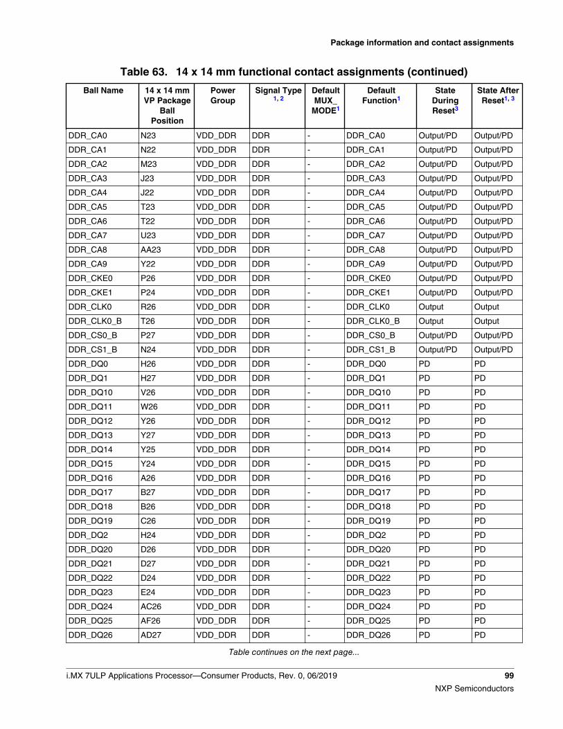
Table 63. 14 x 14 mm functional contact assignments (continued)
Ball Name 14 x 14 mmVP Package
BallPosition
PowerGroup
Signal Type1, 2
DefaultMUX_
MODE1
DefaultFunction1
StateDuringReset3
State AfterReset1, 3
DDR_CA0 N23 VDD_DDR DDR - DDR_CA0 Output/PD Output/PD
DDR_CA1 N22 VDD_DDR DDR - DDR_CA1 Output/PD Output/PD
DDR_CA2 M23 VDD_DDR DDR - DDR_CA2 Output/PD Output/PD
DDR_CA3 J23 VDD_DDR DDR - DDR_CA3 Output/PD Output/PD
DDR_CA4 J22 VDD_DDR DDR - DDR_CA4 Output/PD Output/PD
DDR_CA5 T23 VDD_DDR DDR - DDR_CA5 Output/PD Output/PD
DDR_CA6 T22 VDD_DDR DDR - DDR_CA6 Output/PD Output/PD
DDR_CA7 U23 VDD_DDR DDR - DDR_CA7 Output/PD Output/PD
DDR_CA8 AA23 VDD_DDR DDR - DDR_CA8 Output/PD Output/PD
DDR_CA9 Y22 VDD_DDR DDR - DDR_CA9 Output/PD Output/PD
DDR_CKE0 P26 VDD_DDR DDR - DDR_CKE0 Output/PD Output/PD
DDR_CKE1 P24 VDD_DDR DDR - DDR_CKE1 Output/PD Output/PD
DDR_CLK0 R26 VDD_DDR DDR - DDR_CLK0 Output Output
DDR_CLK0_B T26 VDD_DDR DDR - DDR_CLK0_B Output Output
DDR_CS0_B P27 VDD_DDR DDR - DDR_CS0_B Output/PD Output/PD
DDR_CS1_B N24 VDD_DDR DDR - DDR_CS1_B Output/PD Output/PD
DDR_DQ0 H26 VDD_DDR DDR - DDR_DQ0 PD PD
DDR_DQ1 H27 VDD_DDR DDR - DDR_DQ1 PD PD
DDR_DQ10 V26 VDD_DDR DDR - DDR_DQ10 PD PD
DDR_DQ11 W26 VDD_DDR DDR - DDR_DQ11 PD PD
DDR_DQ12 Y26 VDD_DDR DDR - DDR_DQ12 PD PD
DDR_DQ13 Y27 VDD_DDR DDR - DDR_DQ13 PD PD
DDR_DQ14 Y25 VDD_DDR DDR - DDR_DQ14 PD PD
DDR_DQ15 Y24 VDD_DDR DDR - DDR_DQ15 PD PD
DDR_DQ16 A26 VDD_DDR DDR - DDR_DQ16 PD PD
DDR_DQ17 B27 VDD_DDR DDR - DDR_DQ17 PD PD
DDR_DQ18 B26 VDD_DDR DDR - DDR_DQ18 PD PD
DDR_DQ19 C26 VDD_DDR DDR - DDR_DQ19 PD PD
DDR_DQ2 H24 VDD_DDR DDR - DDR_DQ2 PD PD
DDR_DQ20 D26 VDD_DDR DDR - DDR_DQ20 PD PD
DDR_DQ21 D27 VDD_DDR DDR - DDR_DQ21 PD PD
DDR_DQ22 D24 VDD_DDR DDR - DDR_DQ22 PD PD
DDR_DQ23 E24 VDD_DDR DDR - DDR_DQ23 PD PD
DDR_DQ24 AC26 VDD_DDR DDR - DDR_DQ24 PD PD
DDR_DQ25 AF26 VDD_DDR DDR - DDR_DQ25 PD PD
DDR_DQ26 AD27 VDD_DDR DDR - DDR_DQ26 PD PD
Table continues on the next page...
Package information and contact assignments
i.MX 7ULP Applications Processor—Consumer Products, Rev. 0, 06/2019 99
NXP Semiconductors

Table 63. 14 x 14 mm functional contact assignments (continued)
Ball Name 14 x 14 mmVP Package
BallPosition
PowerGroup
Signal Type1, 2
DefaultMUX_
MODE1
DefaultFunction1
StateDuringReset3
State AfterReset1, 3
DDR_DQ27 AD26 VDD_DDR DDR - DDR_DQ27 PD PD
DDR_DQ28 AF27 VDD_DDR DDR - DDR_DQ28 PD PD
DDR_DQ29 AG26 VDD_DDR DDR - DDR_DQ29 PD PD
DDR_DQ3 J24 VDD_DDR DDR - DDR_DQ3 PD PD
DDR_DQ30 AE25 VDD_DDR DDR - DDR_DQ30 PD PD
DDR_DQ31 AF25 VDD_DDR DDR - DDR_DQ31 PD PD
DDR_DQ4 K24 VDD_DDR DDR - DDR_DQ4 PD PD
DDR_DQ5 K27 VDD_DDR DDR - DDR_DQ5 PD PD
DDR_DQ6 K26 VDD_DDR DDR - DDR_DQ6 PD PD
DDR_DQ7 L26 VDD_DDR DDR - DDR_DQ7 PD PD
DDR_DQ8 V24 VDD_DDR DDR - DDR_DQ8 PD PD
DDR_DQ9 V27 VDD_DDR DDR - DDR_DQ9 PD PD
DDR_DQM0 M24 VDD_DDR DDR - DDR_DQM0 Output/PD Output/PD
DDR_DQM1 T27 VDD_DDR DDR - DDR_DQM1 Output/PD Output/PD
DDR_DQM2 G26 VDD_DDR DDR - DDR_DQM2 Output/PD Output/PD
DDR_DQM3 AA24 VDD_DDR DDR - DDR_DQM3 Output/PD Output/PD
DDR_DQS0 M26 VDD_DDR DDR - DDR_DQS0 Hi-Z Hi-Z
DDR_DQS0_B M27 VDD_DDR DDR - DDR_DQS0_B Hi-Z Hi-Z
DDR_DQS1 U24 VDD_DDR DDR - DDR_DQS1 Hi-Z Hi-Z
DDR_DQS1_B T24 VDD_DDR DDR - DDR_DQS1_B Hi-Z Hi-Z
DDR_DQS2 F27 VDD_DDR DDR - DDR_DQS2 Hi-Z Hi-Z
DDR_DQS2_B F26 VDD_DDR DDR - DDR_DQS2_B Hi-Z Hi-Z
DDR_DQS3 AB26 VDD_DDR DDR - DDR_DQS3 Hi-Z Hi-Z
DDR_DQS3_B AB27 VDD_DDR DDR - DDR_DQS3_B Hi-Z Hi-Z
DSI_CLK_N M2 VDD_DSI18 MIPI DSIPHY
- DSI_CLK_N - -
DSI_CLK_P M1 VDD_DSI18 MIPI DSIPHY
- DSI_CLK_P - -
DSI_DATA0_N P2 VDD_DSI18 MIPI DSIPHY
- DSI_DATA0_N - -
DSI_DATA0_P P1 VDD_DSI18 MIPI DSIPHY
- DSI_DATA0_P - -
DSI_DATA1_N L4 VDD_DSI18 MIPI DSIPHY
- DSI_DATA1_N - -
DSI_DATA1_P M4 VDD_DSI18 MIPI DSIPHY
- DSI_DATA1_P - -
EXTAL AB2 VDD_PMC18 Analog - EXTAL - -
Table continues on the next page...
Package information and contact assignments
100 i.MX 7ULP Applications Processor—Consumer Products, Rev. 0, 06/2019
NXP Semiconductors

Table 63. 14 x 14 mm functional contact assignments (continued)
Ball Name 14 x 14 mmVP Package
BallPosition
PowerGroup
Signal Type1, 2
DefaultMUX_
MODE1
DefaultFunction1
StateDuringReset3
State AfterReset1, 3
EXTAL32 W4 VDD_VBAT18_CAP
Analog - EXTAL32 - -
HSIC_DATA D4 VDD_HSIC DDR - HSIC_DATA Input/PD Input/PD
HSIC_STROBE D5 VDD_HSIC DDR - HSIC_STROBE Input/PD Input/PD
ONOFF Y2 VDD_VBAT18_CAP
SNVS - ONOFF Input/PU Input/PU
PMIC_ON_REQ V1 VDD_VBAT18_CAP
SNVS - PMIC_ON_REQ Output/High Output/High
PTA0 AE14 VDD_PTA FSGPIO 0000b CMP0_IN1_3V Input Hi-Z
PTA1 AF13 VDD_PTA FSGPIO 0000b CMP0_IN2_3V Input Hi-Z
PTA2 AG14 VDD_PTA FSGPIO 0000b CMP1_IN2_3V Input Hi-Z
PTA3 AF14 VDD_PTA FSGPIO 0000b CMP1_IN4_3V Input Hi-Z
PTA4 AD15 VDD_PTA FSGPIO 0000b ADC1_CH3A Input Hi-Z
PTA5 AC15 VDD_PTA FSGPIO 0000b ADC1_CH3B Input Hi-Z
PTA6 AB15 VDD_PTA FSGPIO 0000b ADC1_CH4A/5A/6A/7A/8A
Input Hi-Z
PTA7 AD14 VDD_PTA FSGPIO 0000b ADC1_CH4B/5B/6B/7B/8B
Input Hi-Z
PTA8 AB16 VDD_PTA FSGPIO 0000b ADC1_CH4A/5A/6A/7A/8A
Input Hi-Z
PTA9 AC16 VDD_PTA FSGPIO 0000b ADC1_CH4B/5B/6B/7B/8B
Input Hi-Z
PTA10 AD16 VDD_PTA FSGPIO 0000b ADC1_CH4A/5A/6A/7A/8A
Input Hi-Z
PTA11 AD18 VDD_PTA FSGPIO 0000b ADC1_CH4B/5B/6B/7B/8B
Input Hi-Z
PTA12 AG16 VDD_PTA FSGPIO 0000b ADC1_CH4A/5A/6A/7A/8A
Input Hi-Z
PTA13 AF16 VDD_PTA FSGPIO 0000b ADC1_CH4B/5B/6B/7B/8B
Input Hi-Z
PTA14 AF17 VDD_PTA FSGPIO 0000b ADC1_CH4A/5A/6A/7A/8A
Input Hi-Z
PTA15 AF18 VDD_PTA FSGPIO 0000b ADC1_CH4B/5B/6B/7B/8B
Input Hi-Z
PTA16 AG18 VDD_PTA FSGPIO 0000b CMP1_IN5_3V Hi-Z Hi-Z
PTA17 AD19 VDD_PTA FSGPIO 0000b CMP1_IN6_3V Hi-Z Hi-Z
PTA18 AC19 VDD_PTA FSGPIO 0000b CMP1_IN1_3V Hi-Z Hi-Z
PTA19 AB19 VDD_PTA FSGPIO 0000b CMP1_IN3_3V Hi-Z Hi-Z
PTA20 AD22 VDD_PTA FSGPIO 0000b ADC0_CH8A/9A/10A
Hi-Z Hi-Z
Table continues on the next page...
Package information and contact assignments
i.MX 7ULP Applications Processor—Consumer Products, Rev. 0, 06/2019 101
NXP Semiconductors

Table 63. 14 x 14 mm functional contact assignments (continued)
Ball Name 14 x 14 mmVP Package
BallPosition
PowerGroup
Signal Type1, 2
DefaultMUX_
MODE1
DefaultFunction1
StateDuringReset3
State AfterReset1, 3
PTA21 AB20 VDD_PTA FSGPIO 0000b ADC0_CH8B/9B/10B
Hi-Z Hi-Z
PTA22 AC20 VDD_PTA FSGPIO 0000b ADC0_CH8A/9A/10A
Hi-Z Hi-Z
PTA23 AD20 VDD_PTA FSGPIO 0000b ADC0_CH8B/9B/10B
Hi-Z Hi-Z
PTA24 AF20 VDD_PTA FSGPIO 0000b ADC0_CH8A/9A/10A
Hi-Z Hi-Z
PTA25 AG20 VDD_PTA FSGPIO 0000b ADC0_CH8B/9B/10B
Hi-Z Hi-Z
PTA26 AF21 VDD_PTA FSGPIO 1010b JTAG_TMS/SWD_DIO
Input/PU Input/PU
PTA27 AF22 VDD_PTA FSGPIO 1010b JTAG_TDO Hi-Z Hi-Z
PTA28 AG22 VDD_PTA FSGPIO 1010b JTAG_TDI Input/PU Input/PU
PTA29 AD23 VDD_PTA FSGPIO 1010b JTAG_TCLK/SWD_CLK
Input/PD Input/PD
PTA30 AD24 VDD_PTA FSGPIO 1010b JTAG_TRST_B Input/PU Input/PU
PTA31 AF24 VDD_PTA FSGPIO 0000b ADC0_CH1B Hi-Z Hi-Z
PTB0 AG2 VDD_PTB FSGPIO 0000b ADC0_CH0A Hi-Z Hi-Z
PTB1 AF2 VDD_PTB FSGPIO 0000b ADC0_CH0B Hi-Z Hi-Z
PTB2 AE3 VDD_PTB FSGPIO 0000b ADC0_CH4A/5A/6A
Hi-Z Hi-Z
PTB3 AE4 VDD_PTB FSGPIO 0000b ADC0_CH4B/5B/6B
Hi-Z Hi-Z
PTB4 AG4 VDD_PTB FSGPIO 0000b BT_MODE0 Input/PD PD
PTB5 AF4 VDD_PTB FSGPIO 0000b BT_MODE1 Input/PD PD
PTB6 AF5 VDD_PTB FSGPIO 0000b ADC1_CH1A Hi-Z Hi-Z
PTB7 AF6 VDD_PTB FSGPIO 0000b ADC1_CH1B Hi-Z Hi-Z
PTB8 AG6 VDD_PTB FSGPIO 0000b ADC0_CH14A/CMP0_IN0
Hi-Z Hi-Z
PTB9 AD7 VDD_PTB FSGPIO 0000b ADC0_CH14B/CMP0_IN2
Hi-Z Hi-Z
PTB10 AC7 VDD_PTB FSGPIO 0000b CMP0_IN1 Hi-Z Hi-Z
PTB11 AB7 VDD_PTB FSGPIO 0000b CMP0_IN3 Hi-Z Hi-Z
PTB12 AC8 VDD_PTB FSGPIO 0000b ADC1_CH13A/CMP1_IN0
Hi-Z Hi-Z
PTB13 AD8 VDD_PTB FSGPIO 0000b ADC1_CH13B/CMP1_IN1
Hi-Z Hi-Z
PTB14 AG8 VDD_PTB FSGPIO 0000b ADC1_CH2A Hi-Z Hi-Z
PTB15 AF8 VDD_PTB FSGPIO 0000b ADC1_CH2B Hi-Z Hi-Z
Table continues on the next page...
Package information and contact assignments
102 i.MX 7ULP Applications Processor—Consumer Products, Rev. 0, 06/2019
NXP Semiconductors

Table 63. 14 x 14 mm functional contact assignments (continued)
Ball Name 14 x 14 mmVP Package
BallPosition
PowerGroup
Signal Type1, 2
DefaultMUX_
MODE1
DefaultFunction1
StateDuringReset3
State AfterReset1, 3
PTB16 AF9 VDD_PTB FSGPIO 0000b ADC0_CH4A/5A/6A
Hi-Z Hi-Z
PTB17 AF10 VDD_PTB FSGPIO 0000b ADC0_CH4B/5B/6B
Hi-Z Hi-Z
PTB18 AG10 VDD_PTB FSGPIO 0000b ADC0_CH4A/5A/6A
Hi-Z Hi-Z
PTB19 AD10 VDD_PTB FSGPIO 0000b ADC0_CH4B/5B/6B
Hi-Z Hi-Z
PTC0 D18 VDD_PTC FSGPIO 0000b - Hi-Z Hi-Z
PTC1 E17 VDD_PTC FSGPIO 0000b - Hi-Z Hi-Z
PTC2 F17 VDD_PTC FSGPIO 0000b - Hi-Z Hi-Z
PTC3 G17 VDD_PTC FSGPIO 0000b - Hi-Z Hi-Z
PTC4 F16 VDD_PTC FSGPIO 0000b - Hi-Z Hi-Z
PTC5 D17 VDD_PTC FSGPIO 0000b - Hi-Z Hi-Z
PTC6 D16 VDD_PTC FSGPIO 0000b - Hi-Z Hi-Z
PTC7 G16 VDD_PTC FSGPIO 0000b - Hi-Z Hi-Z
PTC8 A16 VDD_PTC FSGPIO 0000b - Hi-Z Hi-Z
PTC9 B16 VDD_PTC FSGPIO 0000b - Hi-Z Hi-Z
PTC10 B15 VDD_PTC FSGPIO 0000b - Hi-Z Hi-Z
PTC11 B14 VDD_PTC FSGPIO 0000b - Hi-Z Hi-Z
PTC12 A14 VDD_PTC FSGPIO 0000b - Hi-Z Hi-Z
PTC13 D13 VDD_PTC FSGPIO 0000b - Hi-Z Hi-Z
PTC14 E13 VDD_PTC FSGPIO 0000b - Hi-Z Hi-Z
PTC15 F13 VDD_PTC FSGPIO 0000b - Hi-Z Hi-Z
PTC16 G13 VDD_PTC FSGPIO 0000b - Hi-Z Hi-Z
PTC17 G12 VDD_PTC FSGPIO 0000b - Hi-Z Hi-Z
PTC18 F12 VDD_PTC FSGPIO 0000b - Hi-Z Hi-Z
PTC19 E12 VDD_PTC FSGPIO 0000b - Hi-Z Hi-Z
PTD0 A24 VDD_PTD STGPIO 0000b - Hi-Z Hi-Z
PTD1 B24 VDD_PTD STGPIO 0000b - Hi-Z Hi-Z
PTD2 B23 VDD_PTD STGPIO 0000b - Hi-Z Hi-Z
PTD3 B22 VDD_PTD STGPIO 0000b - Hi-Z Hi-Z
PTD4 A22 VDD_PTD STGPIO 0000b - Hi-Z Hi-Z
PTD5 B21 VDD_PTD STGPIO 0000b - Hi-Z Hi-Z
PTD6 B22 VDD_PTD STGPIO 0000b - Hi-Z Hi-Z
PTD7 A20 VDD_PTD STGPIO 0000b - Hi-Z Hi-Z
PTD8 B20 VDD_PTD STGPIO 0000b - Hi-Z Hi-Z
Table continues on the next page...
Package information and contact assignments
i.MX 7ULP Applications Processor—Consumer Products, Rev. 0, 06/2019 103
NXP Semiconductors

Table 63. 14 x 14 mm functional contact assignments (continued)
Ball Name 14 x 14 mmVP Package
BallPosition
PowerGroup
Signal Type1, 2
DefaultMUX_
MODE1
DefaultFunction1
StateDuringReset3
State AfterReset1, 3
PTD9 B19 VDD_PTD STGPIO 0000b - Hi-Z Hi-Z
PTD10 B18 VDD_PTD STGPIO 0000b - Hi-Z Hi-Z
PTD11 A18 VDD_PTD STGPIO 0000b - Hi-Z Hi-Z
PTE0 D12 VDD_PTE FSGPIO 0000b - Hi-Z Hi-Z
PTE1 A12 VDD_PTE FSGPIO 0000b - Hi-Z Hi-Z
PTE2 B12 VDD_PTE FSGPIO 0000b - Hi-Z Hi-Z
PTE3 B11 VDD_PTE FSGPIO 0000b - Hi-Z Hi-Z
PTE4 B10 VDD_PTE FSGPIO 0000b - Hi-Z Hi-Z
PTE5 A10 VDD_PTE FSGPIO 0000b - Hi-Z Hi-Z
PTE6 D9 VDD_PTE FSGPIO 0000b - Hi-Z Hi-Z
PTE7 E8 VDD_PTE FSGPIO 0000b - Hi-Z Hi-Z
PTE8 F9 VDD_PTE FSGPIO 0000b - Hi-Z Hi-Z
PTE9 G9 VDD_PTE FSGPIO 0000b - Hi-Z Hi-Z
PTE10 D8 VDD_PTE FSGPIO 0000b - Hi-Z Hi-Z
PTE11 A8 VDD_PTE FSGPIO 0000b - Hi-Z Hi-Z
PTE12 B8 VDD_PTE FSGPIO 0000b - Hi-Z Hi-Z
PTE13 B7 VDD_PTE FSGPIO 0000b - Hi-Z Hi-Z
PTE14 B6 VDD_PTE FSGPIO 0000b - Hi-Z Hi-Z
PTE15 A6 VDD_PTE FSGPIO 0000b - Hi-Z Hi-Z
PTF0 D2 VDD_PTF FSGPIO 0000b - Input Hi-Z
PTF1 B2 VDD_PTF FSGPIO 0000b - Input Hi-Z
PTF2 B3 VDD_PTF FSGPIO 0000b - Input Hi-Z
PTF3 C3 VDD_PTF FSGPIO 0000b - Input Hi-Z
PTF4 E2 VDD_PTF FSGPIO 0000b - Input Hi-Z
PTF5 B1 VDD_PTF FSGPIO 0000b - Input Hi-Z
PTF6 A2 VDD_PTF FSGPIO 0000b - Input Hi-Z
PTF7 F2 VDD_PTF FSGPIO 0000b - Input Hi-Z
PTF8 F1 VDD_PTF FSGPIO 0000b - Input Hi-Z
PTF9 D1 VDD_PTF FSGPIO 0000b - Input Hi-Z
PTF10 G5 VDD_PTF FSGPIO 0000b - Input Hi-Z
PTF11 G6 VDD_PTF FSGPIO 0000b - Input Hi-Z
PTF12 H7 VDD_PTF FSGPIO 0000b - Input Hi-Z
PTF13 H6 VDD_PTF FSGPIO 0000b - Input Hi-Z
PTF14 H5 VDD_PTF FSGPIO 0000b - Input Hi-Z
PTF15 H4 VDD_PTF FSGPIO 0000b - Input Hi-Z
PTF16 H1 VDD_PTF FSGPIO 0000b - Hi-Z Hi-Z
Table continues on the next page...
Package information and contact assignments
104 i.MX 7ULP Applications Processor—Consumer Products, Rev. 0, 06/2019
NXP Semiconductors

Table 63. 14 x 14 mm functional contact assignments (continued)
Ball Name 14 x 14 mmVP Package
BallPosition
PowerGroup
Signal Type1, 2
DefaultMUX_
MODE1
DefaultFunction1
StateDuringReset3
State AfterReset1, 3
PTF17 H2 VDD_PTF FSGPIO 0000b - Hi-Z Hi-Z
PTF18 J2 VDD_PTF FSGPIO 0000b - Hi-Z Hi-Z
PTF19 K2 VDD_PTF FSGPIO 0000b - Hi-Z Hi-Z
RESET0_B AC11 VDD_PTB RESET - RESET0_B Output/OD Input/PU
RESET1_B K1 VDD_PTF RESET - RESET1_B Output/OD Input/PU
STANDBY_REQ V2 VDD_VBAT18_CAP
SNVS - STANDBY_REQ Output/Low Output/Low
TAMPER V4 VDD_VBAT18_CAP
SNVS - TAMPER Hi-Z4 Input
TESTCLK_N AA8 VDD_PTB - - TESTCLK_N - -
TESTCLK_P AB8 VDD_PTB - - TESTCLK_P - -
USB0_DM T2 VDD_USB33 USB PHY - USB0_DM - -
USB0_DP T1 VDD_USB33 USB PHY - USB0_DP - -
USB0_VBUS_DETECT
T4 VDD_USB33 USB PHY - USB0_VBUS_DETECT
- -
XTAL AA2 VDD_PMC18 Analog - XTAL - -
XTAL32 Y4 VDD_VBAT18_CAP
Analog - XTAL32 - -
1. The state immediately after RESET and before ROM firmware or software has executed.2. FSGPIO = Failsafe GPIOs; STGPIO - Standard GPIOs3. PD = internal pull-down enabled; PU = internal pull-up enabled; OD = open-drain4. TAMPER is Hi-Z during VBAT domain POR and an input otherwise.
9.2 BGA, 10 x 10 mm, 0.5 mm pitch (VK suffix)This section includes the following information for the 10 x 10 mm, 0.5 mm pitchpackage (VK suffix):
• Case outline• Ball map• Contact assignments
9.2.1 10 x 10 mm package case outline
The following figure shows the top, bottom, and side views of the 10 × 10 mm BGApackage.
Package information and contact assignments
i.MX 7ULP Applications Processor—Consumer Products, Rev. 0, 06/2019 105
NXP Semiconductors

Figure 40. 10 x 10 mm case outline
Package information and contact assignments
106 i.MX 7ULP Applications Processor—Consumer Products, Rev. 0, 06/2019
NXP Semiconductors

Figure 41. Notes on 10 x 10 mm case outline
9.2.2 10 x 10 mm, 0.5 mm pitch, ball map
The following page shows the 10 × 10 mm, 0.5 mm pitch, ball map.
Package information and contact assignments
i.MX 7ULP Applications Processor—Consumer Products, Rev. 0, 06/2019 107
NXP Semiconductors

1 2 3 4 5 6 7 8 9 10 11 12 13 14 15 16 17 18 19
A VSS HSIC_DATA HSIC_STROBE VDD18_HSIC PTE6 PTE5 PTE3 PTE1 PTC18 PTC14 PTC13 PTC8 PTC7 PTD5 PTD0 PTD1 VSS DDR_DQ19 VSS A
B PTF2 VSS PTF6 VSS PTE15 PTE7 PTE11 PTE12 PTC19 PTC12 PTC11 PTC9 PTC6 PTD4 PTD2 VSS DDR_DQ16 VSS DDR_DQ22 B
C PTF9 PTF7 PTF1 PTF0 PTF5 PTE14 PTE10 VDD_PTE PTE0 VDD_PTC VSS PTC5 PTC1 PTD7 VDD_PTD DDR_DQ17 DDR_DQ18 DDR_DQ20 DDR_DQS2 C
D PTF14 PTF13 PTF10 PTF12 VSS VDD_HSIC VSS VDD_PTE PTC16 VDD_PTC VSS PTC2 PTD10 PTD9 VDD_PTD DDR_DQ1 DDR_DQ0 DDR_DQ23 DDR_DQS2_B D
E PTF17 PTF16 VSS VDD_PTF PTF11 PTF3 PTE8 PTE13 PTE4 PTC15 PTC10 PTC0 PTD6 PTD3 VSS DDR_DQ7 DDR_DQ5 DDR_DQM2 DDR_VREF0 E
F DSI_DATA1_N PTF18 PTF8 VDD_PTF PTF4 PTF19 VDD18_IOREF PTE9 PTE2 PTC17 PTC4 PTC3 PTD11 PTD8 VSS VDD18_DDR DDR_DQ21 DDR_DQ4 DDR_DQ3 F
G DSI_DATA1_P VSS PTF15 RESET1_B VDD_PTF VSS VDD_DIG1 VDD_DIG1 VDD_DIG1 VDD_DIG1 VDD_DIG1 VDD_DIG1 VDD_DIG1 VSS VDD_DDR DDR_DQ2 DDR_DQ6 DDR_CA4 DDR_DQS0 G
H DSI_CLK_P DSI_CLK_N VSS VDD_DSI18 VSS VSS VDD_DIG1 VSS VSS VSS VSS VSS VDD_DIG1 VSS VDD_DDR DDR_CS1_B DDR_CA3 DDR_DQM0 DDR_DQS0_B H
J DSI_DATA0_P DSI_DATA0_N VSS VDD_DSI11 VSS VSS VDD_DIG1 VSS VSS VSS VSS VSS VDD_DIG1 VSS VDD_DDR DDR_CA2 DDR_CKE1 DDR_CA1 DDR_CA0 J
K USB0_DP VDD_USB18 VDD_USB33 USB0_VBUS_DETECT
VDD_VBAT18_CAP VSS VSS VSS VSS VSS VSS VSS VDD_DIG1 VSS VDD_DDR DDR_CKE0 VSS DDR_CS0_B DDR_CLK0 K
L USB0_DM VSS VDD_VBAT42 VSS VSS VSS VSS VSS VSS VSS VSS VSS VDD_DIG1 VSS VDD_DDR DDR_CA8 DDR_CA5 DDR_CA6 DDR_CLK0_B L
M VSS VSS VSS STANDBY_REQ TAMPER VSS VSS VDD_PMC18_DIG0
VSS VSS VSS VSS VDD_DIG1 VSS VDD_DDR DDR_DQ9 DDR_CA7 DDR_DQM1 DDR_DQS1_B M
N EXTAL32 PMIC_ON_REQ ONOFF VSS VDD_PLL18 VDD_PTB PTB4VDD_PMC18_DI
G0VDD_PMC18_DI
G0VSS VDD_PMC11_DI
G0_CAPVDD_DIG0 VDD_DIG1 VSS VDD_DDR DDR_CA9 DDR_ODT DDR_DQ8 DDR_DQS1 N
P XTAL32 VSS_ANA VSS VDD_PMC18VDD_PMC11_DI
G1_CAPPTB9 VDD_ANA33 VDD_ANA18 PTA4 VSS VDD_PMC11_DI
G0_CAPVDD_DIG0 VSS VSS VDD_DDR DDR_DQ25 VSS DDR_DQ11 DDR_DQ12 P
R VSS VSS VDD_PMC12_DIG1
VDD_PMC12_DIG1
VDD_PMC11_DIG1_CAP
PTB11 PTB13 PTB16 PTA7 VDD_PTA VDD_PTA PTA12 PTA16 PTA30 DDR_DQ31 DDR_DQ29 DDR_DQ10 DDR_DQ15 DDR_VREF1 R
T XTAL0 VSS PTB2 PTB3 PTB10 PTB12 PTB5 PTB15 PTA0 PTA6 PTA8 PTA14 PTA18 PTA21 PTA31 DDR_DQ13 DDR_DQ14 DDR_DQM3 DDR_DQS3_B T
U EXTAL0 VSS VSS PTB0 VSS PTB6 PTB17 VSS_ADC_ANA PTA9 VSS PTA10 PTA17 VSS PTA19 PTA29 PTA27 DDR_DQ30 DDR_DQ26 DDR_DQS3 U
V VSS VSS PTB1 TESTCLK_P PTB7 PTB18 DAC0_OUT DAC1_OUT PTA1 PTA3 PTA5 PTA15 PTA11 PTA24 PTA20 PTA26 DDR_ZQ0 VSS DDR_DQ24 V
W VSS PTB8 PTB14 TESTCLK_N PTB19 RESET0_B VSS_ADC_ANA VREFH_ANA18 VREFL_ANA VSS_ADC_ANA PTA2 PTA13 PTA25 PTA23 PTA22 PTA28 DDR_DQ28 DDR_DQ27 VSS W
1 2 3 4 5 6 7 8 9 10 11 12 13 14 15 16 17 18 19
Package information and contact assignments
108
NXP Semiconductors
i.MX 7ULP Applications Processor—Consumer Products, Rev. 0, 06/2019
10 x 10 mm, 0.5 mm pitch, ball map

9.2.3 10 x 10 mm power supply and functional contactassignments
The following table shows the power supply contact assignments for the 10 × 10 mmpackage.
Table 64. 10 x 10 mm power supply contact assignments
Supply Name 10x10 mm VK Package BallPosition
Remarks
DDR_ODT N17 DDR on-die termination
DDR_VREF0 E19 DDR voltage reference input. Connect to a voltagesource that is 50% of VDD_DDR.
DDR_VREF1 R19 DDR voltage reference input. Connect to a voltagesource that is 50% of VDD_DDR.
DDR_ZQ0 V17 Connect DDR_ZQ0 to an external 240Ω 1% resistorto Vss.This is a reference used during DDR outputbuffer driver calibration.
TESTCLK_N W4 Test function for NXP use only. This output mustremain unconnected.
TESTCLK_P V4 Test function for NXP use only. This output mustremain unconnected.
USB0_VBUS K4 USB0 VBUS detection
VDD_ANA18 P8 ADC analog and IO 1.8V supply input
VDD_ANA33 P7 ADC analog and IO 3.3V supply input
VDD_DDR G15, H15, J15, K15, L15, M15, N15,P15
DDR I/O supply input
VDD_DIG0 N12, P12 M4 domain core and logic supply input
VDD_DIG1 G7, G8, G9, G10, G11, G12, G13,H7, H13, J7, J13, K13, L13, M13,N13
A7 domain core and logic supply input
VDD_DSI11 J4 MIPI DSI 1.1V supply input
VDD_DSI18 H4 MIPI DSI 1.8V supply input
VDD_HSIC D6 HSIC 1.2V supply input
VDD_PLL18 N5 PLL analog supply input
VDD_PMC11_DIG0_CAP N11, P11 M4 domain LDO supply output
VDD_PMC11_DIG1_CAP P5, R5 A7 domain LDO supply output
VDD_PMC12_DIG1 R3, R4 A7 domain LDO and internal memory LDO supplyinput
VDD_PMC18 P4 M4/A7 PMC and PMC IO supply input
VDD_PMC18_DIG0 M8, N8, N9 M4 domain LDO and internal memory LDO supplyinput
VDD_PTA R10, R11 GPIO Port A supply input
Table continues on the next page...
Package information and contact assignments
i.MX 7ULP Applications Processor—Consumer Products, Rev. 0, 06/2019 109
NXP Semiconductors

Table 64. 10 x 10 mm power supply contact assignments (continued)
Supply Name 10x10 mm VK Package BallPosition
Remarks
VDD_PTB N6 GPIO Port B supply input
VDD_PTC C10, D10 GPIO Port C supply input
VDD_PTD C15, D15 GPIO Port D supply input
VDD_PTE C8, D8 GPIO Port E supply input
VDD_PTF E4, F4, G5 GPIO Port F supply input
VDD_USB18 K2 USB PHY 1.8V supply input
VDD_USB33 K3 USB PHY 3.3V supply input
VDD_VBAT18_CAP K5 SNVS domain LDO output
VDD_VBAT42 L3 SNVS domain LDO supply input
VDD18_DDR F16 DDR 1.8V pre-driver supply input
VDD18_HSIC A4 HSIC 1.8V supply input
VDD18_IOREF F7 1.8V IO supply reference and A7 supply referenceinput
VREFH_ANA18 W8 ADC high reference supply input
VREFL_ANA W9 ADC low reference supply input
VSS A1, A17, A19, B2, B4, B16, B18,C11, D5, D7, D11, E3, E15, F15,G2, G14, H3, H5, H6, H8, H9, H10,H11, H12, H14, J3, J5, J6, J8, J9,J10, J11, J12, J14, K6, K7, K8, K9,K10, K11, K12, K14, K17, L2, L4,L5, L6, L7, L8, L9, L10, L11, L12,L14, M1, M2, M3, M6, M7, M9, M10,M11, M12, M14, N4, N10, N14, P2,P3, P10, P13, P14, P17, R1, R2,T2, U2, U3, U5, U10, U13V1, V2,V18, W1, W19
Ground
VSS_ADC_ANA U8, W7, W10 ADC analog ground
The following table shows functional contact assignments for the 10 x 10 mm package.
Table 65. 10 x 10 mm functional contact assignments
Ball Name 10 x 10 mmVK Package
BallPosition
PowerGroup
Signal Type1, 2
DefaultMUX_
MODE1
DefaultFunction1
StateDuringReset3
State AfterReset1, 3
DAC0_OUT V7 VDD_ANA18 Analog - DAC0_OUT - -
DAC1_OUT V8 VDD_ANA18 Analog - DAC1_OUT - -
DDR_CA0 J19 VDD_DDR DDR - DDR_CA0 Output/PD Output/PD
DDR_CA1 J18 VDD_DDR DDR - DDR_CA1 Output/PD Output/PD
DDR_CA2 J16 VDD_DDR DDR - DDR_CA2 Output/PD Output/PD
Table continues on the next page...
Package information and contact assignments
110 i.MX 7ULP Applications Processor—Consumer Products, Rev. 0, 06/2019
NXP Semiconductors

Table 65. 10 x 10 mm functional contact assignments (continued)
Ball Name 10 x 10 mmVK Package
BallPosition
PowerGroup
Signal Type1, 2
DefaultMUX_
MODE1
DefaultFunction1
StateDuringReset3
State AfterReset1, 3
DDR_CA3 H17 VDD_DDR DDR - DDR_CA3 Output/PD Output/PD
DDR_CA4 G18 VDD_DDR DDR - DDR_CA4 Output/PD Output/PD
DDR_CA5 L17 VDD_DDR DDR - DDR_CA5 Output/PD Output/PD
DDR_CA6 L18 VDD_DDR DDR - DDR_CA6 Output/PD Output/PD
DDR_CA7 M17 VDD_DDR DDR - DDR_CA7 Output/PD Output/PD
DDR_CA8 L16 VDD_DDR DDR - DDR_CA8 Output/PD Output/PD
DDR_CA9 N16 VDD_DDR DDR - DDR_CA9 Output/PD Output/PD
DDR_CKE0 K16 VDD_DDR DDR - DDR_CKE0 Output/PD Output/PD
DDR_CKE1 J17 VDD_DDR DDR - DDR_CKE1 Output/PD Output/PD
DDR_CLK0 K19 VDD_DDR DDR - DDR_CLK0 Output Output
DDR_CLK0_B L19 VDD_DDR DDR - DDR_CLK0_B Output Output
DDR_CS0_B K18 VDD_DDR DDR - DDR_CS0_B Output/PD Output/PD
DDR_CS1_B H16 VDD_DDR DDR - DDR_CS1_B Output/PD Output/PD
DDR_DQ0 D17 VDD_DDR DDR - DDR_DQ0 PD PD
DDR_DQ1 D16 VDD_DDR DDR - DDR_DQ1 PD PD
DDR_DQ10 R17 VDD_DDR DDR - DDR_DQ10 PD PD
DDR_DQ11 P18 VDD_DDR DDR - DDR_DQ11 PD PD
DDR_DQ12 P19 VDD_DDR DDR - DDR_DQ12 PD PD
DDR_DQ13 T16 VDD_DDR DDR - DDR_DQ13 PD PD
DDR_DQ14 T17 VDD_DDR DDR - DDR_DQ14 PD PD
DDR_DQ15 R18 VDD_DDR DDR - DDR_DQ15 PD PD
DDR_DQ16 B17 VDD_DDR DDR - DDR_DQ16 PD PD
DDR_DQ17 C16 VDD_DDR DDR - DDR_DQ17 PD PD
DDR_DQ18 C17 VDD_DDR DDR - DDR_DQ18 PD PD
DDR_DQ19 A18 VDD_DDR DDR - DDR_DQ19 PD PD
DDR_DQ2 G16 VDD_DDR DDR - DDR_DQ2 PD PD
DDR_DQ20 C18 VDD_DDR DDR - DDR_DQ20 PD PD
DDR_DQ21 F17 VDD_DDR DDR - DDR_DQ21 PD PD
DDR_DQ22 B19 VDD_DDR DDR - DDR_DQ22 PD PD
DDR_DQ23 D18 VDD_DDR DDR - DDR_DQ23 PD PD
DDR_DQ24 V19 VDD_DDR DDR - DDR_DQ24 PD PD
DDR_DQ25 P16 VDD_DDR DDR - DDR_DQ25 PD PD
DDR_DQ26 U18 VDD_DDR DDR - DDR_DQ26 PD PD
DDR_DQ27 W18 VDD_DDR DDR - DDR_DQ27 PD PD
DDR_DQ28 W17 VDD_DDR DDR - DDR_DQ28 PD PD
DDR_DQ29 R16 VDD_DDR DDR - DDR_DQ29 PD PD
Table continues on the next page...
Package information and contact assignments
i.MX 7ULP Applications Processor—Consumer Products, Rev. 0, 06/2019 111
NXP Semiconductors

Table 65. 10 x 10 mm functional contact assignments (continued)
Ball Name 10 x 10 mmVK Package
BallPosition
PowerGroup
Signal Type1, 2
DefaultMUX_
MODE1
DefaultFunction1
StateDuringReset3
State AfterReset1, 3
DDR_DQ3 F19 VDD_DDR DDR - DDR_DQ3 PD PD
DDR_DQ30 U17 VDD_DDR DDR - DDR_DQ30 PD PD
DDR_DQ31 R15 VDD_DDR DDR - DDR_DQ31 PD PD
DDR_DQ4 F18 VDD_DDR DDR - DDR_DQ4 PD PD
DDR_DQ5 E17 VDD_DDR DDR - DDR_DQ5 PD PD
DDR_DQ6 G17 VDD_DDR DDR - DDR_DQ6 PD PD
DDR_DQ7 E16 VDD_DDR DDR - DDR_DQ7 PD PD
DDR_DQ8 N18 VDD_DDR DDR - DDR_DQ8 PD PD
DDR_DQ9 M16 VDD_DDR DDR - DDR_DQ9 PD PD
DDR_DQM0 H18 VDD_DDR DDR - DDR_DQM0 Output/PD Output/PD
DDR_DQM1 M18 VDD_DDR DDR - DDR_DQM1 Output/PD Output/PD
DDR_DQM2 E18 VDD_DDR DDR - DDR_DQM2 Output/PD Output/PD
DDR_DQM3 T18 VDD_DDR DDR - DDR_DQM3 Output/PD Output/PD
DDR_DQS0 G19 VDD_DDR DDR - DDR_DQS0 Hi-Z Hi-Z
DDR_DQS0_B H19 VDD_DDR DDR - DDR_DQS0_B Hi-Z Hi-Z
DDR_DQS1 N19 VDD_DDR DDR - DDR_DQS1 Hi-Z Hi-Z
DDR_DQS1_B M19 VDD_DDR DDR - DDR_DQS1_B Hi-Z Hi-Z
DDR_DQS2 C19 VDD_DDR DDR - DDR_DQS2 Hi-Z Hi-Z
DDR_DQS2_B D19 VDD_DDR DDR - DDR_DQS2_B Hi-Z Hi-Z
DDR_DQS3 U19 VDD_DDR DDR - DDR_DQS3 Hi-Z Hi-Z
DDR_DQS3_B T19 VDD_DDR DDR - DDR_DQS3_B Hi-Z Hi-Z
DSI_CLK_N H2 VDD_DSI18 MIPI DSIPHY
- DSI_CLK_N - -
DSI_CLK_P H1 VDD_DSI18 MIPI DSIPHY
- DSI_CLK_P - -
DSI_DATA0_N J2 VDD_DSI18 MIPI DSIPHY
- DSI_DATA0_N - -
DSI_DATA0_P J1 VDD_DSI18 MIPI DSIPHY
- DSI_DATA0_P - -
DSI_DATA1_N F1 VDD_DSI18 MIPI DSIPHY
- DSI_DATA1_N - -
DSI_DATA1_P G1 VDD_DSI18 MIPI DSIPHY
- DSI_DATA1_P - -
EXTAL U1 VDD_PMC18 Analog - EXTAL - -
EXTAL32 N1 VDD_VBAT18_CAP
Analog - EXTAL32 - -
HSIC_DATA A2 VDD_HSIC DDR - HSIC_DATA Input/PD Input/PD
HSIC_STROBE A3 VDD_HSIC DDR - HSIC_STROBE Input/PD Input/PD
Table continues on the next page...
Package information and contact assignments
112 i.MX 7ULP Applications Processor—Consumer Products, Rev. 0, 06/2019
NXP Semiconductors

Table 65. 10 x 10 mm functional contact assignments (continued)
Ball Name 10 x 10 mmVK Package
BallPosition
PowerGroup
Signal Type1, 2
DefaultMUX_
MODE1
DefaultFunction1
StateDuringReset3
State AfterReset1, 3
ONOFF N3 VDD_VBAT18_CAP
SNVS - ONOFF Input/PU Input/PU
PMIC_ON_REQ M4 VDD_VBAT18_CAP
SNVS - PMIC_ON_REQ Output/High Output/High
PTA0 T9 VDD_PTA FSGPIO 0000b CMP0_IN1_3V Input Hi-Z
PTA1 V9 VDD_PTA FSGPIO 0000b CMP0_IN2_3V Input Hi-Z
PTA2 W11 VDD_PTA FSGPIO 0000b CMP1_IN2_3V Input Hi-Z
PTA3 V10 VDD_PTA FSGPIO 0000b CMP1_IN4_3V Input Hi-Z
PTA4 P9 VDD_PTA FSGPIO 0000b ADC1_CH3A Input Hi-Z
PTA5 V11 VDD_PTA FSGPIO 0000b ADC1_CH3B Input Hi-Z
PTA6 T10 VDD_PTA FSGPIO 0000b ADC1_CH4A/5A/6A/7A/8A
Input Hi-Z
PTA7 R9 VDD_PTA FSGPIO 0000b ADC1_CH4B/5B/6B/7B/8B
Input Hi-Z
PTA8 T11 VDD_PTA FSGPIO 0000b ADC1_CH4A/5A/6A/7A/8A
Input Hi-Z
PTA9 U9 VDD_PTA FSGPIO 0000b ADC1_CH4B/5B/6B/7B/8B
Input Hi-Z
PTA10 U11 VDD_PTA FSGPIO 0000b ADC1_CH4A/5A/6A/7A/8A
Input Hi-Z
PTA11 V13 VDD_PTA FSGPIO 0000b ADC1_CH4B/5B/6B/7B/8B
Input Hi-Z
PTA12 R12 VDD_PTA FSGPIO 0000b ADC1_CH4A/5A/6A/7A/8A
Input Hi-Z
PTA13 W12 VDD_PTA FSGPIO 0000b ADC1_CH4B/5B/6B/7B/8B
Input Hi-Z
PTA14 T12 VDD_PTA FSGPIO 0000b ADC1_CH4A/5A/6A/7A/8A
Input Hi-Z
PTA15 V12 VDD_PTA FSGPIO 0000b ADC1_CH4B/5B/6B/7B/8B
Input Hi-Z
PTA16 R13 VDD_PTA FSGPIO 0000b CMP1_IN5_3V Hi-Z Hi-Z
PTA17 U12 VDD_PTA FSGPIO 0000b CMP1_IN6_3V Hi-Z Hi-Z
PTA18 T13 VDD_PTA FSGPIO 0000b CMP1_IN1_3V Hi-Z Hi-Z
PTA19 U14 VDD_PTA FSGPIO 0000b CMP1_IN3_3V Hi-Z Hi-Z
PTA20 V15 VDD_PTA FSGPIO 0000b ADC0_CH8A/9A/10A
Hi-Z Hi-Z
PTA21 T14 VDD_PTA FSGPIO 0000b ADC0_CH8B/9B/10B
Hi-Z Hi-Z
PTA22 W15 VDD_PTA FSGPIO 0000b ADC0_CH8A/9A/10A
Hi-Z Hi-Z
Table continues on the next page...
Package information and contact assignments
i.MX 7ULP Applications Processor—Consumer Products, Rev. 0, 06/2019 113
NXP Semiconductors

Table 65. 10 x 10 mm functional contact assignments (continued)
Ball Name 10 x 10 mmVK Package
BallPosition
PowerGroup
Signal Type1, 2
DefaultMUX_
MODE1
DefaultFunction1
StateDuringReset3
State AfterReset1, 3
PTA23 W14 VDD_PTA FSGPIO 0000b ADC0_CH8B/9B/10B
Hi-Z Hi-Z
PTA24 V14 VDD_PTA FSGPIO 0000b ADC0_CH8A/9A/10A
Hi-Z Hi-Z
PTA25 W13 VDD_PTA FSGPIO 0000b ADC0_CH8B/9B/10B
Hi-Z Hi-Z
PTA26 V16 VDD_PTA FSGPIO 1010b JTAG_TMS/SWD_DIO
Input/PU Input/PU
PTA27 U16 VDD_PTA FSGPIO 1010b JTAG_TDO Hi-Z Hi-Z
PTA28 W16 VDD_PTA FSGPIO 1010b JTAG_TDI Input/PU Input/PU
PTA29 U15 VDD_PTA FSGPIO 1010b JTAG_TCLK/SWD_CLK
Input/PD Input/PD
PTA30 R14 VDD_PTA FSGPIO 1010b JTAG_TRST_B Input/PU Input/PU
PTA31 T15 VDD_PTA FSGPIO 0000b ADC0_CH1B Hi-Z Hi-Z
PTB0 U4 VDD_PTB FSGPIO 0000b ADC0_CH0A Hi-Z Hi-Z
PTB1 V3 VDD_PTB FSGPIO 0000b ADC0_CH0B Hi-Z Hi-Z
PTB2 T3 VDD_PTB FSGPIO 0000b ADC0_CH4A/5A/6A
Hi-Z Hi-Z
PTB3 T4 VDD_PTB FSGPIO 0000b ADC0_CH4B/5B/6B
Hi-Z Hi-Z
PTB4 N7 VDD_PTB FSGPIO 0000b BT_MODE0 Input/PD PD
PTB5 T7 VDD_PTB FSGPIO 0000b BT_MODE1 Input/PD PD
PTB6 U6 VDD_PTB FSGPIO 0000b ADC1_CH1A Hi-Z Hi-Z
PTB7 V5 VDD_PTB FSGPIO 0000b ADC1_CH1B Hi-Z Hi-Z
PTB8 W2 VDD_PTB FSGPIO 0000b ADC0_CH14A/CMP0_IN0
Hi-Z Hi-Z
PTB9 P6 VDD_PTB FSGPIO 0000b ADC0_CH14B/CMP0_IN2
Hi-Z Hi-Z
PTB10 T5 VDD_PTB FSGPIO 0000b CMP0_IN1 Hi-Z Hi-Z
PTB11 R6 VDD_PTB FSGPIO 0000b CMP0_IN3 Hi-Z Hi-Z
PTB12 T6 VDD_PTB FSGPIO 0000b ADC1_CH13A/CMP1_IN0
Hi-Z Hi-Z
PTB13 R7 VDD_PTB FSGPIO 0000b ADC1_CH13B/CMP1_IN1
Hi-Z Hi-Z
PTB14 W3 VDD_PTB FSGPIO 0000b ADC1_CH2A Hi-Z Hi-Z
PTB15 T8 VDD_PTB FSGPIO 0000b ADC1_CH2B Hi-Z Hi-Z
PTB16 R8 VDD_PTB FSGPIO 0000b ADC0_CH4A/5A/6A
Hi-Z Hi-Z
PTB17 U7 VDD_PTB FSGPIO 0000b ADC0_CH4B/5B/6B
Hi-Z Hi-Z
Table continues on the next page...
Package information and contact assignments
114 i.MX 7ULP Applications Processor—Consumer Products, Rev. 0, 06/2019
NXP Semiconductors

Table 65. 10 x 10 mm functional contact assignments (continued)
Ball Name 10 x 10 mmVK Package
BallPosition
PowerGroup
Signal Type1, 2
DefaultMUX_
MODE1
DefaultFunction1
StateDuringReset3
State AfterReset1, 3
PTB18 V6 VDD_PTB FSGPIO 0000b ADC0_CH4A/5A/6A
Hi-Z Hi-Z
PTB19 W5 VDD_PTB FSGPIO 0000b ADC0_CH4B/5B/6B
Hi-Z Hi-Z
PTC0 E12 VDD_PTC FSGPIO 0000b - Hi-Z Hi-Z
PTC1 C13 VDD_PTC FSGPIO 0000b - Hi-Z Hi-Z
PTC2 D12 VDD_PTC FSGPIO 0000b - Hi-Z Hi-Z
PTC3 F12 VDD_PTC FSGPIO 0000b - Hi-Z Hi-Z
PTC4 F11 VDD_PTC FSGPIO 0000b - Hi-Z Hi-Z
PTC5 C12 VDD_PTC FSGPIO 0000b - Hi-Z Hi-Z
PTC6 B13 VDD_PTC FSGPIO 0000b - Hi-Z Hi-Z
PTC7 A13 VDD_PTC FSGPIO 0000b - Hi-Z Hi-Z
PTC8 A12 VDD_PTC FSGPIO 0000b - Hi-Z Hi-Z
PTC9 B12 VDD_PTC FSGPIO 0000b - Hi-Z Hi-Z
PTC10 E11 VDD_PTC FSGPIO 0000b - Hi-Z Hi-Z
PTC11 B11 VDD_PTC FSGPIO 0000b - Hi-Z Hi-Z
PTC12 B10 VDD_PTC FSGPIO 0000b - Hi-Z Hi-Z
PTC13 A11 VDD_PTC FSGPIO 0000b - Hi-Z Hi-Z
PTC14 A10 VDD_PTC FSGPIO 0000b - Hi-Z Hi-Z
PTC15 D10 VDD_PTC FSGPIO 0000b - Hi-Z Hi-Z
PTC16 D9 VDD_PTC FSGPIO 0000b - Hi-Z Hi-Z
PTC17 F10 VDD_PTC FSGPIO 0000b - Hi-Z Hi-Z
PTC18 A9 VDD_PTC FSGPIO 0000b - Hi-Z Hi-Z
PTC19 B9 VDD_PTC FSGPIO 0000b - Hi-Z Hi-Z
PTD0 A15 VDD_PTD STGPIO 0000b - Hi-Z Hi-Z
PTD1 A16 VDD_PTD STGPIO 0000b - Hi-Z Hi-Z
PTD2 B15 VDD_PTD STGPIO 0000b - Hi-Z Hi-Z
PTD3 E14 VDD_PTD STGPIO 0000b - Hi-Z Hi-Z
PTD4 B14 VDD_PTD STGPIO 0000b - Hi-Z Hi-Z
PTD5 A14 VDD_PTD STGPIO 0000b - Hi-Z Hi-Z
PTD6 E13 VDD_PTD STGPIO 0000b - Hi-Z Hi-Z
PTD7 C14 VDD_PTD STGPIO 0000b - Hi-Z Hi-Z
PTD8 F14 VDD_PTD STGPIO 0000b - Hi-Z Hi-Z
PTD9 D14 VDD_PTD STGPIO 0000b - Hi-Z Hi-Z
PTD10 D13 VDD_PTD STGPIO 0000b - Hi-Z Hi-Z
PTD11 F13 VDD_PTD STGPIO 0000b - Hi-Z Hi-Z
Table continues on the next page...
Package information and contact assignments
i.MX 7ULP Applications Processor—Consumer Products, Rev. 0, 06/2019 115
NXP Semiconductors
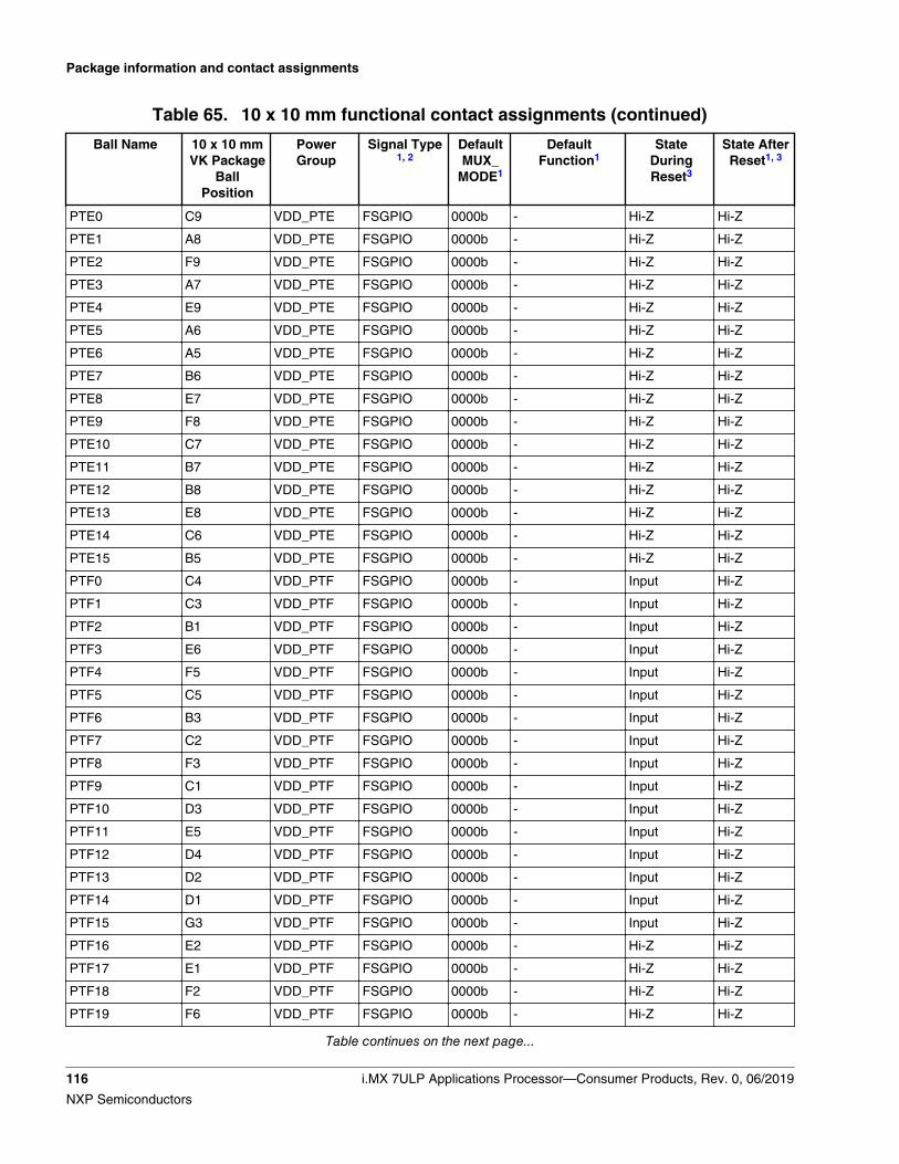
Table 65. 10 x 10 mm functional contact assignments (continued)
Ball Name 10 x 10 mmVK Package
BallPosition
PowerGroup
Signal Type1, 2
DefaultMUX_
MODE1
DefaultFunction1
StateDuringReset3
State AfterReset1, 3
PTE0 C9 VDD_PTE FSGPIO 0000b - Hi-Z Hi-Z
PTE1 A8 VDD_PTE FSGPIO 0000b - Hi-Z Hi-Z
PTE2 F9 VDD_PTE FSGPIO 0000b - Hi-Z Hi-Z
PTE3 A7 VDD_PTE FSGPIO 0000b - Hi-Z Hi-Z
PTE4 E9 VDD_PTE FSGPIO 0000b - Hi-Z Hi-Z
PTE5 A6 VDD_PTE FSGPIO 0000b - Hi-Z Hi-Z
PTE6 A5 VDD_PTE FSGPIO 0000b - Hi-Z Hi-Z
PTE7 B6 VDD_PTE FSGPIO 0000b - Hi-Z Hi-Z
PTE8 E7 VDD_PTE FSGPIO 0000b - Hi-Z Hi-Z
PTE9 F8 VDD_PTE FSGPIO 0000b - Hi-Z Hi-Z
PTE10 C7 VDD_PTE FSGPIO 0000b - Hi-Z Hi-Z
PTE11 B7 VDD_PTE FSGPIO 0000b - Hi-Z Hi-Z
PTE12 B8 VDD_PTE FSGPIO 0000b - Hi-Z Hi-Z
PTE13 E8 VDD_PTE FSGPIO 0000b - Hi-Z Hi-Z
PTE14 C6 VDD_PTE FSGPIO 0000b - Hi-Z Hi-Z
PTE15 B5 VDD_PTE FSGPIO 0000b - Hi-Z Hi-Z
PTF0 C4 VDD_PTF FSGPIO 0000b - Input Hi-Z
PTF1 C3 VDD_PTF FSGPIO 0000b - Input Hi-Z
PTF2 B1 VDD_PTF FSGPIO 0000b - Input Hi-Z
PTF3 E6 VDD_PTF FSGPIO 0000b - Input Hi-Z
PTF4 F5 VDD_PTF FSGPIO 0000b - Input Hi-Z
PTF5 C5 VDD_PTF FSGPIO 0000b - Input Hi-Z
PTF6 B3 VDD_PTF FSGPIO 0000b - Input Hi-Z
PTF7 C2 VDD_PTF FSGPIO 0000b - Input Hi-Z
PTF8 F3 VDD_PTF FSGPIO 0000b - Input Hi-Z
PTF9 C1 VDD_PTF FSGPIO 0000b - Input Hi-Z
PTF10 D3 VDD_PTF FSGPIO 0000b - Input Hi-Z
PTF11 E5 VDD_PTF FSGPIO 0000b - Input Hi-Z
PTF12 D4 VDD_PTF FSGPIO 0000b - Input Hi-Z
PTF13 D2 VDD_PTF FSGPIO 0000b - Input Hi-Z
PTF14 D1 VDD_PTF FSGPIO 0000b - Input Hi-Z
PTF15 G3 VDD_PTF FSGPIO 0000b - Input Hi-Z
PTF16 E2 VDD_PTF FSGPIO 0000b - Hi-Z Hi-Z
PTF17 E1 VDD_PTF FSGPIO 0000b - Hi-Z Hi-Z
PTF18 F2 VDD_PTF FSGPIO 0000b - Hi-Z Hi-Z
PTF19 F6 VDD_PTF FSGPIO 0000b - Hi-Z Hi-Z
Table continues on the next page...
Package information and contact assignments
116 i.MX 7ULP Applications Processor—Consumer Products, Rev. 0, 06/2019
NXP Semiconductors

Table 65. 10 x 10 mm functional contact assignments (continued)
Ball Name 10 x 10 mmVK Package
BallPosition
PowerGroup
Signal Type1, 2
DefaultMUX_
MODE1
DefaultFunction1
StateDuringReset3
State AfterReset1, 3
RESET0_B W6 VDD_PTB RESET - RESET0_B Output/OD Input/PU
RESET1_B G4 VDD_PTF RESET - RESET1_B Output/OD Input/PU
STANDBY_REQ M4 VDD_VBAT18_CAP
SNVS - STANDBY_REQ Output/Low Output/Low
TAMPER M5 VDD_VBAT18_CAP
SNVS - TAMPER Hi-Z4 Input
TESTCLK_N W4 VDD_PTB - - TESTCLK_N - -
TESTCLK_P V4 VDD_PTB - - TESTCLK_P - -
USB0_DM L1 VDD_USB33 USB PHY - USB0_DM - -
USB0_DP K1 VDD_USB33 USB PHY - USB0_DP - -
USB0_VBUS_DETECT
K4 VDD_USB33 USB PHY - USB0_VBUS_DETECT
- -
XTAL T1 VDD_PMC18 Analog - XTAL - -
XTAL32 P1 VDD_VBAT18_CAP
Analog - XTAL32 - -
1. The state immediately after RESET and before ROM firmware or software has executed.2. FSGPIO = Failsafe GPIOs; STGPIO - Standard GPIOs3. PD = internal pull-down enabled; PU = internal pull-up enabled; OD = open-drain4. TAMPER is Hi-Z during VBAT domain POR and an input otherwise.
10 Revision HistoryThe following table provides a revision history for this document.
Table 66. Revision History
Rev. No. Date Substantial Changes
0 06/2019 Initial public release
Revision History
i.MX 7ULP Applications Processor—Consumer Products, Rev. 0, 06/2019 117
NXP Semiconductors

How to Reach Us:
Home Page:nxp.com
Web Support:nxp.com/support
Information in this document is provided solely to enable system and software implementers to use
NXP products. There are no express or implied copyright licenses granted hereunder to design or
fabricate any integrated circuits based on the information in this document. NXP reserves the right to
make changes without further notice to any products herein.
NXP makes no warranty, representation, or guarantee regarding the suitability of its products for any
particular purpose, nor does NXP assume any liability arising out of the application or use of any
product or circuit, and specifically disclaims any and all liability, including without limitation
consequential or incidental damages. “Typical” parameters that may be provided in NXP data sheets
and/or specifications can and do vary in different applications, and actual performance may vary over
time. All operating parameters, including “typicals,” must be validated for each customer application
by customerʼs technical experts. NXP does not convey any license under its patent rights nor the
rights of others. NXP sells products pursuant to standard terms and conditions of sale, which can be
found at the following address: nxp.com/SalesTermsandConditions.
While NXP has implemented advanced security features, all products may be subject to unidentified
vulnerabilities. Customers are responsible for the design and operation of their applications and
products to reduce the effect of these vulnerabilities on customer's applications and products, and
NXP accepts no liability for any vulnerability that is discovered. Customers should implement
appropriate design and operating safeguards to minimize the risks associated with their applications
and products.
NXP, the NXP logo, NXP SECURE CONNECTIONS FOR A SMARTER WORLD, COOLFLUX,
EMBRACE, GREENCHIP, HITAG, I2C BUS, ICODE, JCOP, LIFE VIBES, MIFARE, MIFARE
CLASSIC, MIFARE DESFire, MIFARE PLUS, MIFARE FLEX, MANTIS, MIFARE ULTRALIGHT,
MIFARE4MOBILE, MIGLO, NTAG, ROADLINK, SMARTLX, SMARTMX, STARPLUG, TOPFET,
TRENCHMOS, UCODE, Freescale, the Freescale logo, AltiVec, C-5, CodeTEST, CodeWarrior,
ColdFire, ColdFire+, C-Ware, the Energy Efficient Solutions logo, Kinetis, Layerscape, MagniV,
mobileGT, PEG, PowerQUICC, Processor Expert, QorIQ, QorIQ Qonverge, Ready Play, SafeAssure,
the SafeAssure logo, StarCore, Symphony, VortiQa, Vybrid, Airfast, BeeKit, BeeStack, CoreNet,
Flexis, MXC, Platform in a Package, QUICC Engine, SMARTMOS, Tower, TurboLink, and UMEMS
are trademarks of NXP B.V. All other product or service names are the property of their respective
owners. AMBA, Arm, Arm7, Arm7TDMI, Arm9, Arm11, Artisan, big.LITTLE, Cordio, CoreLink,
CoreSight, Cortex, DesignStart, DynamIQ, Jazelle, Keil, Mali, Mbed, Mbed Enabled, NEON, POP,
RealView, SecurCore, Socrates, Thumb, TrustZone, ULINK, ULINK2, ULINK-ME, ULINK-PLUS,
ULINKpro, μVision, Versatile are trademarks or registered trademarks of Arm Limited (or its
subsidiaries) in the US and/or elsewhere. The related technology may be protected by any or all of
patents, copyrights, designs and trade secrets. All rights reserved. Oracle and Java are registered
trademarks of Oracle and/or its affiliates. The Power Architecture and Power.org word marks and the
Power and Power.org logos and related marks are trademarks and service marks licensed by
Power.org.
© 2019 NXP B.V.
Document Number IMX7ULPCECRevision 0, 06/2019