process-structure-property relationship and its impact … · abstract−microelectronics device...
TRANSCRIPT

JOURNAL OF SEMICONDUCTOR TECHNOLOGY AND SCIENCE, VOL.3, NO. 3, SEPTEMBER, 2003
107
Manuscript received August 1, 2003; revised August 27, 2003. Institute of Microelectronics, 11 Science Park Rd., Science park II,
Singapore 117685, Rep. of Singapore. TEL: 65-6770-537, FAX: 65-6774-5747 Email: [email protected]
Process-Structure-Property Relationship and its Impact on Microelectronics Device Reliability and Failure
Mechanism
Chih Hang TUNG
Abstract−Microelectronics device performance
and its reliability are directly related to and controlled by its constituent materials and their microstructure. Specific processes used to form and shape the materials microstructure need to be controlled in order to achieve the ultimate device performance. Examples of front-end and back-end ULSI processes, packaging process, and novel optical storage materials are given to illustrate such process-structure-property-reliability relationship. As more novel materials are introduced to meet the new requirements for device shrinkage, such under-standing is indispensable for future generation process development and reliability assessment.
Index Terms−Reliability, ESD Electronigration
Leadframe, CD-RW
I. INTRODUCTION
The majority of microelectronics device failures can
be eventually traced back to the materials used unable to
sustain the stresses applied, being electrical stress,
mechanical stress, thermal stress, or environmental stress.
When the materials unable to withstand the stresses, the
system free energy and entropy fluctuate and the
materials microstructure alters, either suddenly and
causes immediately materials property changes and leads
to device malfunction, or slowly and progressively leads
to function degradation and eventually device failure.
Well known example for the former case is gate
dielectric breakdown, where charge built-up in gate
dielectric leads to a sudden increase in gate leakage
current, induces gate oxide rupture and physical damages
to the gate oxide, substrate channel, and gate electrodes.
Example for the later case is electromigration with
gradual resistivity increment and eventually leads to the
final metal line open. In both cases, materials
microstructure undergoes detectable changes and can be
captured by failure analysis. These changes are noted as
“failure mechanisms” in a failure analysis.
Apparently the materials used to build up the device
plays an important role in deciding not just the device
functionality but also the device reliability. The
processes, which used to grow and form the materials to
its desired shape, size, and microstructure in the device,
are in turn deciding the materials property. This process-
structure-property-reliability relationship is the key in
understanding the microelectronics process related
reliability issues.
In this article, a few examples in different areas are
presented to illustrate the process related reliability
issues. Reliability degradation associated with specific
process or materials will be emphasized.
II. ESD IMPLANTATION AND ESD FAILURES
Gate oxide edge, usually is the location with strong
electrical field and low conduction resistivity (when
overlapped with s/d junction), is the place where most

CHIH HANG TUNG : PROCESS-STRUCTURE-PROPERTY RELATIONSHIP AND ITS IMPACT ON MICROELECTRONICS…
108
Fig. 1. ESD discharge damages at the polygate edge. The
discharge occurred at exactly between the polygate and the
active area, leaving a damage mark on Si substrate as shown
here.
Fig. 2. Plan view TEM shows ESD implantation induced mask
edge defect. Poly gate is preserved for easy identification of the
location of mask edge defects. The mask edge defects acted as
a dislocation source and pumped out extended dislocations.
gate oxide hard breakdown occurred [1, 2]. Fig 1 shows
an ESD discharge induced gate oxide edge break down.
Both SEM and TEM plan view images showed the
breakdown occurred exactly at the edge of polygate and
the active area (on the drain side only). The damage
spots are multiple in locations, creating small cut marks
on Si substrate. The well known approach is to improve
the breakdown voltage by extra ion implantation on the
active area edge. This is usually called ESD implantation.
However, extra implantation introduced extra lattice
defects. ESD implantation can cause severe mask edge
defects (MED), which then evolves into extended
dislocations in subsequent process steps. Fig 2 shows
ESD implantation induced mask edge defects that have
evolved into extended dislocations. The dislocation lines
can introduce junction leakage or to the least, greatly
reduce the device capability to sustain ESD surge stress.
This is an example of process induced defects, which
greatly degrades the device reliability.
III. CU ELECTROMIGRATION AND
MICROSTRUCTURE
Cu metallization is a well accepted alternative to
conventional Al metallization for technology nodes
beyond 180nm. The adhesion and texture of Cu
demonstrate a strong dependence on barrier materials [3].
The adhesion of barrier to the underlying dielectric can
depend on out-gassing of moisture and other organic
species from the dielectric surface during barrier
deposition [4]. Interface adhesion has been proven to be
the key in the success of Cu technology in a wafer
fabrication. The critical interfaces include SiN/Cu, Cu/Ta
(or TaN), and Ta/dielectrics. Fig 3(a) shows a worst case
with improper process conditions where total dela-
mination occurs at the Cu/TaN interface.
Ta or TaN barrier needs to sustain Cu attack at various
aggressive process conditions. To improve its capability
as a diffusion barrier, double layered Ta with one
crystalline and one amorphous layer is created, as shown
in Fig 3(b). The advantage of such a dual barrier has
been proven. However, in a dual damascene process with
high aspect ratio vertical VIA side wall, double-layered
barrier may not be easily achievable, Fig 3(c). More than
often the sidewall Ta barrier quality is poor. This is

JOURNAL OF SEMICONDUCTOR TECHNOLOGY AND SCIENCE, VOL.3, NO. 3, SEPTEMBER, 2003
109
Fig. 3. (a) Cu metallization total lift off from the Ta barrier
metal due to improper Ta/Cu interface cleanliness. (b) TaN
barrier layer formed different microstructures in different
locations. Crystalline phase is observed in horizontal film near
Cu, location A. Amorphous phase observed in horizontal film
near oxide, location B. (c) Amorphous columnar, and porous,
on the contact side wall, location C.
clearly demonstrated in Fig 4. Poor step coverage Cu
barrier metal can leads to Cu spiking into Si substrate
and junction leakage. The importance of interfaces in Cu
technology cannot be overly emphasized. It has been
demonstrated that Cu electromigration depends strongly
on the SiN/Cu and Cu/Ta interfaces properties [5, 6].
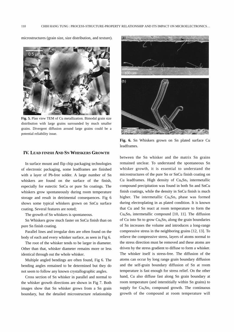
Cu film, in as electroplated condition, was found to
have extremely fine grain structure. However, the grain
size was found to grow to more than 1 µm in diameter
over time, even at room temperature [7]. Such
microstructure evolution was accompanied by sheet
resistivity decrement, film internal stress relaxation, and
volume shrinkage. Unfortunately, the grain growth
within Cu film proceeds concurrently with recrysta-
llization, a process that leads to the bimodal grain size
distribution, where large grains are surrounded by much
smaller grains and there are twin peaks in the grain size
distribution. Grain growth is typically a separate process
followed by recrystallization, or secondary grain growth,
where some of the strain free grains grow at the expense
of other grains. In the case of plated Cu thin films, the
Fig. 4. TaN barrier layer formed different microstructures in
different locations, (a). Crystalline phase is observed in
horizontal film near Cu, location A. Amorphous phase
observed in horizontal film near oxide, location B. And
amorphous columnar on the contact side wall, location C. A
weak spot is observed at the contact bottom corner and Cu seep
through into Si, as indicated, (b).
recrystallization process appears to occur simultaneously
with normal grain growth and both of them are
happening at room temperature. Fig 5 shows a typical Cu
film plan view microstructure. Large grains surrounded
by much smaller grains is detrimental in terms of electric
and stress induced migration since diffusion divergence
near the large grains will lead to early failure of the
metallization. A solution to such a problem is to add
impurities into Cu film. Impurities in Cu matrix will act
as grain boundary pining centers during grain growth
and slow down or totally stop the recrystallization from
happening [8].
The Cu metallization process condition and its
subsequent thermal history are the key to achieve robust
interfaces (among Cu, dielectrics, barrier metal) and Cu
CHIH HANG TUNG : PROCESS-STRUCTURE-PROPERTY RELATIONSHIP AND ITS IMPACT ON MICROELECTRONICS…
110
microstructures (grain size, size distribution, and texture).
Fig. 5. Plan view TEM of Cu metallization. Bimodal grain size
distribution with large grains surrounded by much smaller
grains. Divergent diffusion around large grains could be a
potential reliability issue.
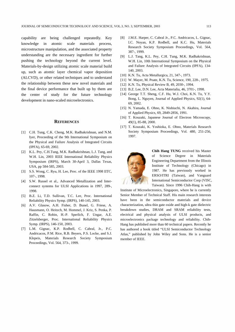
IV. LEAD FINISH AND SN WHISKERS GROWTH
In surface mount and flip chip packaging technologies
of electronic packaging, some leadframes are finished
with a layer of Pb-free solder. A large number of Sn
whiskers are found on the surface of the finish,
especially for eutectic SnCu or pure Sn coatings. The
whiskers grow spontaneously during room temperature
storage and result in detrimental consequences. Fig 6
shows some typical whiskers grown on SnCu surface
coating. Several features are noted;
The growth of Sn whiskers is spontaneous.
Sn Whiskers grow much faster on SnCu finish than on
pure Sn finish coating.
Parallel lines and irregular dots are often found on the
body of each and every whisker surface, as seen in Fig 6.
The root of the whisker tends to be larger in diameter.
Other than that, whisker diameter remains more or less
identical through out the whole whisker.
Multiple angled bendings are often found, Fig 6. The
bending angles remained to be determined but they do
not seem to follow any known crystallographic angles.
Cross section of Sn whisker in parallel and normal to
the whisker growth directions are shown in Fig 7. Both
images show that Sn whisker grows from a Sn grain
boundary, but the detailed microstructure relationship
Fig. 6. Sn Whiskers grown on Sn plated surface Cu
leadframes.
between the Sn whisker and the matrix Sn grains
remained unclear. To understand the spontaneous Sn
whisker growth, it is essential to understand the
microstructures of the pure Sn or SnCu finish coating on
Cu leadframes. High density of Cu6Sn5 intermetallic
compound precipitation was found in both Sn and SnCu
finish coatings, while the density in SnCu finish is much
higher. The intermetallic Cu6Sn5 phase was formed
during electroplating in as plated condition. It is known
that Cu and Sn react at room temperature to form the
Cu6Sn5 intermetallic compound [10, 11]. The diffusion
of Cu into Sn to grow Cu6Sn5 along the grain boundaries
of Sn increases the volume and introduces a long-range
compressive stress in the neighboring grains [12, 13]. To
relieve the compressive stress, layers of atoms normal to
the stress direction must be removed and these atoms are
driven by the stress gradient to diffuse to form a whisker.
The whisker itself is stress-free. The diffusion of the
atoms can occur by long range grain boundary diffusion
and the self-grain boundary diffusion of Sn at room
temperature is fast enough for stress relief. On the other
hand, Cu also diffuse fast along Sn grain boundary at
room temperature (and interstitially within Sn grains) to
supply for Cu6Sn5 compound growth. The continuous
growth of the compound at room temperature will

JOURNAL OF SEMICONDUCTOR TECHNOLOGY AND SCIENCE, VOL.3, NO. 3, SEPTEMBER, 2003
111
Fig. 7. Cross section TEM image on the Whisker root (a) along
parallel to whisker grow direction showing the whisker
initiates from a Sn grain boundary, as indicated.(b) along
normal to whisker grow direction.
maintain the compressive stress in the Sn matrix, hence,
Sn whisker growth on Cu leadframe is a spontaneous
phenomenon [14].
The problem can thus be resolved by properly control
the surface coating layer residue stress. It has been
shown that proper finish coating residue stress
management, by controlling the coating process and its
subsequent heat treatment, can effectively remove the Sn
whisker issue.
V. CD-RW MATERIALS MICROSTRUCTURE AND
ITS RELIABILITY
Phase-change optical disk (or CD-rewritable, CD-RW)
is one of the next generation high-density memory media.
Figure 7 Cross section TEM image on the Whisker root
(a) along parallel to whisker grow direction showing the
whisker initiates from a Sn grain boundary, as
indicated.(b) along normal to whisker grow direction.
The information stored is removable and rewritable
with high density and capacity and in average, in a much
lower unit cost than the magnetic media. It is light-
weighted and relatively reliable and insensitive to the
Fig. 8. (a) Cross section TEM image of phase-change optical
disk. The zig-zag morphology are the tracks structures for data
storage with pitch width 740 nm. Data are stored as marks on
both grove and land tracks. (b) Close up of the laminated
structure shows details of each one of the layers, as marked.
environment. In order to compete with its magnetic
media counterparts, however, it is essential to have the
optical disk capable of rewriting the information for
more than a million times without deteriorate the basic
materials and structures.
The basic operation principle for the phase-change
optical disk is quite straightforward. A thin
polycrystalline film is used as the information storage
base materials. The most popular materials are Ge-Sb-Te
ternary alloy or Ag-In-Sb-Te alloy [15]. The material
itself deflects laser photons differently when it is
amorphous compared to when it becomes crystalline
phase, and thus when laser beam hits the materials, the
detector can pick up different signal in amorphous area
and in crystalline area. To make it works properly, a very
thin Ge-Sb-Te alloy, for example 30 nm, is sandwiched
between amorphous ZnS-SiO2 layers [16, 17]. A thick Al
metallization is usually coated on one side of this
lamination to serve as a mirror for light reflection
purpose. The base Ge-Sb-Te material is crystalline, but
when hit by a strong laser, it transform into amorphous
locally and this serve as a single digit information (0 and
1, as amorphous or crystalline or vice versa). The laser

CHIH HANG TUNG : PROCESS-STRUCTURE-PROPERTY RELATIONSHIP AND ITS IMPACT ON MICROELECTRONICS…
112
beams used for read and write information are of
different wave length and energy in such a way that only
the writing laser can induce phase transition but not the
reading laser. As mentioned before, one million times of
information re-write simply means the materials need to
go through one million times of crystalline-amorphous
transition without apparent deterioration of the materials
itself. It is thus, very important to design and control the
quality of the lamination, the thermal dissipation, thin
film deposition quality, interface roughness, and overall
mechanical integrity. Detailed study on the micros-
tructure and phase transformation of the metallurgical
system is of crucial importance in order to understand
the reliability and other related issues.
A typical cross section on such a CD-RW is shown in
Figs 8 and 9. The basic lamination is Al metal thickness
about 90 nm, a ZnS-SiO2 layer around 10 nm, the Ge-
Sb-Te alloy film around 30 nm, and another thicker ZnS-
SiO2 around 65 nm are laminated together.
Polycarbonate is the external substrate material on both
sides of the lamination, and using UV resin for bonding
the whole structure together. The zig-zag pattern
observed in the cross section as seen in Fig 8 is the
“tracks” which define the information read/write
resolution. Typical track pitch is around 0.75 µm for
current CD-RW and can be smaller if blue laser (shorter
wavelength) is used to increase the spatial resolution. As
mentioned, Al film serves as a mirror to reflect the
incoming laser beam back to the detector. It is thus very
critical to have a smooth mirror surface. The Al to ZnS-
SiO2 interface needs to be very smooth, as seen in Fig 8.
It is not important as to how thick the Al is as long as it
reflects the laser photons properly. In fact, non-
homogeneous Al film thickness, as shown in Fig 9 as an
example, is often found locally in most CD-RW disks.
The Ge-Sb-Te alloy film is the layer that possesses the
information storage function. The film is kept very thin
to facilitate the phase transformation reaction. Also
important is the grain size, as it has two important
functions;
Finer grain size of Ge-Sb-Te alloy gives rise to higher
reflectivity and thus distinct itself from amorphous phase
promptly.
Finer grain size of Ge-Sb-Te also facilitates the phase
transition back-and-forth between crystalline and
amorphous phases.
Fig. 9. Cross section TEM of the laminated layers. Large Al
thickness variation can be observed, as indicated. This,
however, does not affect the function of the optical disk since it
is used only as a reflection mirror.
It is thus more desirable to have a nanocrystalline Ge-
Sb-Te alloy film within the CD-RW disks. The alloy is in
a multi-phase equilibrium region with low temperature
eutectic reaction. That is one of the reasons why it is
capable of transforming back-and-forth between
crystalline and amorphous phases swiftly. Microstructure,
in this case, determines the CD-RW performance and its
capability to swiftly transform back-and-forth between
crystalline and amorphous phases for thousands of times
without degradation. How the Ge-Sb-Te thin film
microstructure looks like and how it reacts to laser
ablashion, are the dominant reliability measurement
parameters for CD-RW.
VI. CONCLUSIONS
A few examples are given to illustrate the relationship
among process, structure/property, and reliability of the
microelectronics devices and materials. The examples
cover ULSI front-end-of-line (FEOL) process, back-end-
of-line (BEOL) process, advanced packaging process, as
well as novel CD-RW materials. Alteration in the
materials microstructures, either abruptly or gradually,
inevitably leads to device performance degradation and
eventually leads to device failure.
Our ability to manipulate the materials microstructure
down to the sub-100nm scale is the key to the success of
today’s microelectronics miniaturization. When ULSI
technology is pushed toward atomic scale, such
JOURNAL OF SEMICONDUCTOR TECHNOLOGY AND SCIENCE, VOL.3, NO. 3, SEPTEMBER, 2003
113
capability are being challenged repeatedly. Key
knowledge in atomic scale materials process,
microstructure manipulation, and the associated property
understanding are the necessary ingredient for further
pushing the technology beyond the current level.
Materials-by-design utilizing atomic scale material build
up, such as atomic layer chemical vapor deposition
(ALCVD), or other related techniques and to understand
the relationship between these new novel materials and
the final device performance that built up by them are
the center of study for the future technology
development in nano-scaled microelectronics.
REFERENCES
[1] C.H. Tung, C.K. Cheng, M.K. Radhakrishnan, and N.M. Iyer, Proceeding of the 9th International Symposium on the Physical and Failure Analysis of Integrated Circuits (IPFA), 65-69, 2002.
[2] K.L. Pey, C.H.Tung, M.K. Radhakrishnan, L.J. Tang, and W.H. Lin, 2003 IEEE International Reliability Physics Symposium (IRPS), March 30-April 3, Dallas Texas, USA, pp 584-585, 2003.
[3] S.S. Wong, C. Ryu, H. Lee, Proc. of the IEEE 1998 IITC, 107-, 1998.
[4] S.W. Russel et al., Advanced Metallization and Inter-connect systems for ULSI Applications in 1997, 289-, 1998.
[5] B.Z. Li, T.D. Sullivan, T.C. Lee, Proc. International Reliability Physics Symp. (IRPS), 140-145, 2003.
[6] A.V. Glasow, A.H. Fisher, D. Bunel, G. Friese, A. Hausmann, O. Heitzch, M. Hommel, J. Kriz, S. Penka, P. Raffin, C. Robin, H.-P. Sperlich, F. Ungar, A.E. Zitzelsberger, Proc. International Reliability Physics Symp. (IRPS), 146-150, 2003.
[7] L.M. Gignac, K.P. Rodbell, C. Cabral, Jr., P.C. Andricacos, P.M. Rice, R.B. Beyers, P.S. Locke, and S.J. Klepeis, Materials Research Society Symposium Proceedings, Vol. 564, 373-, 1999.
[8] J.M.E. Harper, C. Cabral Jr., P.C. Andricacos, L. Gignac, I.C. Noyan, K.P. Rodbell, and K.C. Hu, Materials Research Society Symposium Proceedings, Vol. 564, 387-, 1999.
[9] L.J. Tang, K.L. Pey, C.H. Tung, M.K. Radhakrishnan, W.H. Lin, 10th International Symposium on the Physical and Failure Analysis of Integrated Circuits (IPFA), 134-140, 2003.
[10] K.N. Tu, Acta Metallurgica, 21, 347-, 1973. [11] W. Mayer, M. Poate, K.N. Tu, Science, 190, 228-, 1975. [12] K.N. Tu, Physical Review B, 49, 2030-, 1994. [13] B.Z. Lee, D.N. Lee, Acta Materialia, 46, 3701-, 1998. [14] George T.T. Sheng, C.F. Hu, W.J. Choi, K.N. Tu, Y.Y.
Bong, L. Nguyen, Journal of Applied Physics, 92(1), 64-69, 2002.
[15] N. Yamada, E. Ohno, K. Nishiuchi, N. Akahira, Journal of Applied Physics, 69, 2849-2856, 1991.
[16] T. Kouzaki, Japanese Journal of Electron Microscopy, 49(1), 85-88, 2000.
[17] T. Kouzaki, K. Yoshioka, E. Ohno, Materials Research Society Symposium Proceedings, Vol. 480, 251-256, 1997.
Chih Hang TUNG received his Master of Science Degree in Materials Engineering Department from the Illinois Institute of Technology (Chicago) in 1987. He has previously worked in ERSO/ITRI (Taiwan), and Vanguard International Semiconductor Corp (VISC, Taiwan). Since 1996 Chih-Hang is with
Institute of Microelectronics, Singapore, where he is currently Senior Member of Technical Staff. His main research interests have been in the semiconductor materials and device characterization, ultra thin gate oxide and high-k gate dielectric breakdown studies, DRAM and SRAM reliability tests, electrical and physical analysis of ULSI products, and microelectronics package technology and reliability. Chih-Hang has published more than 60 technical papers. Recently he has authored a book titled “ULSI Semiconductor Technology Atlas,” published by John Wiley and Sons. He is a senior member of IEEE.