power gating
TRANSCRIPT

POWER GATINGW A T MAHESH DANANJAYA

STATIC POWER REDUCTION
• In the past few decades dynamic power is the major concern of design
engineers due to fastening the system clock and frequency.
• But prevailing technology revolution with advanced fabrication techniques with
technologies such as photolithography, the device or technology scaling is
happening with an exponential growth.
• Thus semiconductor devices scale down and leakages are becoming
paramount important for the overall power consumption.
• Therefore VLSI power architecture predicts that static power (Leakage Power)
will become a dominant component of the power architecture and most
researches are carrying through to support that concept.
• Power gating are effectively mitigating leakage losses and becomes a major
static power reduction technique.
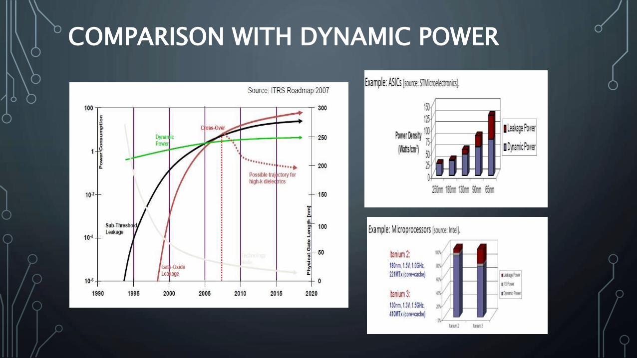
COMPARISON WITH DYNAMIC POWER

POWER GATING
• The basic strategy of power gating is to establish two power modes, Active Mode,
Low Power Mode and switch between these power modes where necessary
• Establishment of two power modes is a pragmatic remedy for accurate switch
between these modes at the appropriate time and in the appropriate manner to
maximize power saving while minimizing the impact on the performance
• Therefore switching and controlling process is also complex
• Due to power gating implementations there may be three modes of operations
• Active Mode
• Sleep (Low power mode)
• Wake Up

SLEEP TRANSISTORS
• Head Sleep Transistor Foot Sleep Transistor

SWITCH SIZING
• Smaller Switches: Smaller area, large resistance and
good leakage reduction
• Bigger Switches: Larger area, smaller resistance and
relatively low leakage reduction

SWITCH PLACING ARCHITECTURE
• Switch in Cell: Switch transistor in each standard cell.
Area overhead is a disadvantage and physical design
easiness of EDA is an advantage

SWITCH PLACING ARCHITECTURE
• Grid of Switches: Switches placed in an array across
the power gated block. 3 rails routed through the logic
block (Power, GND and Virtual).

SWITCH PLACING ARCHITECTURE
• Ring of Switches: Used primarily for legacy design
where the physical design of the block may not be
disturbed.

SIGNAL ISOLATION
• Powering Down the region will not result in crowbar
current in many inputs of powered up blocks.
• None of the floating outputs of the power-down block
will result in spurious behavior in the power-up
blocks. Clams will add some delays to the propagation
paths.

POWER GATING MODES
• Fine Grained Power Gating
• Process of adding a sleep transistor to every cell is called a
fine-grained power gating
• Coarse Grained Power Gating
• Implementation of grid style sleep transistor, to stack of
logic cell, which drive cell locally through shared virtual
power network, is known as coarse grain power gating
• Ring Based
• Power gates (Switches) are places around the perimeter of
the module that is being switched off as a ring
• Column Based
• Power gates are inserted within the module with the cells
abutted to each other in the form of columns

CONTROLLING MECHANISM
• Non-State Preserving Power Gating
• Cut-off (CO)
• Multi-Threshold (MTCMOS
• Boosted-Gate (BGMOS)
• Super Cut-off (SCCMOS)
• State Preserving Power Gating
• Variable Threshold (VTMOS)
• Zigzag Cut Off (ZZCO)
• Zero Delay Ripple Turn On (ZZRTO)
• State Preserving use some retention registers to store states.

STATE RETENTION TECHNIQUES
• When power gating taking place we have to retain some critical state
content (FSM State)
• Software Based Register Read and Write
• Scan Based approach based on using scan chains to store state
off chip
• Retention Registers
RETENTION REGISTERS
• When power gating taking place we have to retain some critical register content (FSM
State).
• Saving and restoring state quickly and efficiently is the faster and power efficient
method to get the block fully functional after power up.
• There can be various methods for state retention.
• DSP Unit: data flow driven DSP unit can start from reset on new data input.
• Cache Processor: This mechanism is good for large residual state retention.
SYNCHRONOUS & ASYNCRONOUS LOGIC POWER GATING
• Clock gating for dynamic power reduction which reduce the power consumption of
idle section of synchronous circuits
• Asynchronous circuits has a inherent strength of data driven capability and active
while performing useful tasks
• Asynchronous circuits implement the equivalent of a fine grain power gating network
• Power gating can be efficiently implemented in Pipelined flows

EDA POWER GATING
Design power gating library cells
Determine which blocks to power gate
Determine state retention mechanism
Determine Rush Current Control Scheme
Design power gating controller
Power gating aware synthesis
Determine floor plan
power gating aware placement
clock tree synthesis
Route
Verify virtual rail electrical characteristics
verify timing