power and delay optimization using power gating
DESCRIPTION
a 6TSRAM has been optimied using power gating techniqueTRANSCRIPT
Dissertation Part II Presentation
Yield Optimization in VLSI Circuits using Power Gating
in
Partial Fulfillment of Degree of Master of Technology (M. Tech.) Semester IVby
Swati S. Kumar(2012PUSETMVLX01587)
(Session 2013-14)
Under supervision ofMr. Gaurav Soni
Assistant Professor
Department of Computer EngineeringSchool of Engineering & Technology
Poornima UniversityIS-2027 to 2031, Ramchandrapura, Sitapura Extension, Jaipur-303905 (Raj.)

Contents
• Introduction•Problem statement• Power Gating • Circuit Implementation• 6TSRAM using Power Gating• Results and Discussions• Conclusion • Future Work• References

Introduction
Moore’s law− transistor count will get 2X in 18 months− get ten fold in every seven years
Fig 1: CMOS Technology Roadmap

Problem statement Increase in Power Dissipation with Technology ScalingIncrease in Leakage Power will slow down speed
P6Pentium ® proc
486
3862868086
80858080
80084004
0.1
1
10
1971 1974 1978 1985 1992 2000Year
Po
wer
(W
atts
)
Fig2: Power increases with decrease in VDD

ObjectiveTo Increase the yield by minimizing the power dissipation and delay.
To predict the performance of the circuits with importance in digital circuits.
To implement the circuit through HSPICE using proposed technique
Formulate the results to achieve the primary aim.

Power Gating
Switch the power OFF to the FU when not needed
Achieved by using a suitably sized header or footer transistor
Popular technique to reduce FU power
Fig 3: Power Gating Technique

Proposed Circuit: 6TSRAM
SRAM- Static Random Access Memory
Fig 4: 6TSRAM Cell
Inverter Inverter
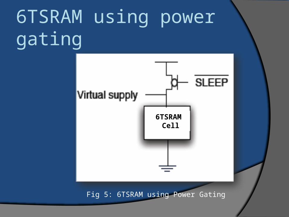
6TSRAM using power gating
6TSRAM Cell
Fig 5: 6TSRAM using Power Gating

Results and Discussions
Without Power Gating With Power Gating
In 32nm technology,Average power of 6TSRAM without using power gating.
( avg_power ) = 4.0940E+18

Results
In 32nm technology,6TSRAM using Power Gating Technique
Average Power( avg_power )= 2.2842E+17

Conclusion
•Power dissipation and delay increment is the critical issue
in VLSI circuits.
•6TSRAM is an important component in electronic circuits
like sensors and cache memory.
•Power Gating is an effective technique to increase yield.
•In 6TSRAM power dissipation has achieved significant
reduction with increase in speed.
•Noise margin need to be reduced in the circuits.

Future WorkPower gating will be applied over larger circuit to achieve the aim in final dissertation.
Noise and area should be reduced to achieve more yield in the circuits.
More attention need to pay over technology scaling.

References

THANKS !!!