portfolio of staff exchange training at astron 2
TRANSCRIPT

Project „Building on Advanced LOFAR Technology for Innovation,
Collaboration, and Sustainability” (Nr. 692257 – BALTICS)
Portfolio of Staff Exchange Training at ASTRON 2
16/12/2016 BALTICS 1
CONTENTS Introduction
BALTICS concept background Objectives Work plan
Measurements of the antennas 1.1 Brief description 1.2. Measurement setup 1.3. S11 measurements 1.4. Directivity measurements
Measurements of the mixer 2.1. Mixer prototype board Nr. 1 2.2. Mixer prototype board Nr. 1 measurement setup 2.3. Mixer prototype board Nr. 1 Vset voltage investigation 2.4. Mixer prototype board Nr. 2 2.5. Mixer prototype board Nr. 2 measurement setup 2.6. Balun test board
Measurements of the SAAM one channel Measurement of the upper signal generator signal power over the spectra Measurement of the system response to weak signal fSGIB=2.4 GHz (-30 dBm, A) Measurement of the system response to signal fSGIB=2.4 GHz (-20 dBm, B) Measurement of the system response to mirror channel signal fSGIB=2.3 GHz (-20 dBm, C) Measurement of the system response to intermodulating signals (-20 dBm, D) Measurement of the filtered system response to signal fSGIB=2.4 GHz (-20 dBm, G) Mixing products measurement (no IF filter) at fSGIB=2.5 GHz (-20 dBm, I) Measurement of the filtered system response to signal fSGIB=2.5 GHz (-20 dBm, H) Measurement of the complete system at fSGIB=1.8 GHz (-20 dBm, J) Measurement of the complete system at fSGIB=1.14 GHz (-20 dBm, K) Measurement of the complete system at fSGIB=0.9 GHz (-20 dBm, L) Measurement of the complete system at fSGIB=1550..3450 MHz (-20 dBm, O) Measurement of the complete system at fSGIB=175..550 MHz (-20 dBm, S)
16/12/2016 BALTICS 2

Introduction
BALTICS concept background
During one-month Staff Exchange Training at ASTRON (in further text – internship) two secondments from VIRAC staff (in further text – apprentices) are introduced to the actual LOFAR hardware, the ASTRON laboratories and further in-depth training through hands-on experience. During this visit, the VIRAC staff is introduced to a wider group of experts at ASTRON such building on a solid network of contacts after returning to Latvia.
Objectives
During this internship the main aim for apprentices is to develop their competences and knowledge in the area of the RFI mainly making measurements of the Small Antenna Array Module (SAAM) building blocks and the complete system. To observe influence of the SAAM building block components on the system, some blocks were designed taking into account final system parameters. Comparison and analysis of the real block implementation parameters and planned block parameters were planned as apprentices knowledge rising instrumentary. In addition, field measurements of the RFI around LOFAR core are planned using equipment from RFI measuring equipment manufacturers and parts made during the internship.
Work plan
The work plan of internship was organised according to the limited amount of practice time. Thus throughout the internship a work meeting with work supervisors from ASTRON once per week was organised where the results of work done in last week were presented and the work plans for next week were discussed. Most of the time apprentices were working independently receiving guidance, instructions and assistance from supervisors whenever necessary.
The main tasks in the work plan of this internship are: ● Measurements of the developed antenna prototypes parameters; ● Measurements of the mixer board parameters; ● Measurements of the complete SAAM system 1 channel up to digital downconverter; ● Preparation of report – Portfolio of Staff Exchange Training at ASTRON 1.
Following chapters describe each task in more detail.
16/12/2016 BALTICS 3

1. Measurements of the antennas
1.1 Brief description
Five different antenna prototypes were made using planar technology. Patch type topology is used for those antennas. Three antennas can be classified as single antennas but two as arrays, see figure 1.1 to 1.5 (two independent antennas for each type).
Fig. 1.1 (type 1) Fig. 1.2 (type 2) Fig. 1.3 (type 3)
Type 1 and type 2 antennas are fed from board bottom side, while type 3 antenna from the board edge (two contact areas in each side of the microstrip line originally was for connector soldering). Patch arrays 2x2 and 4x4 are shown in figures 1.4 and 1.5 respectively.
CST (Computer Simulation Technology) electromagnetic simulation software was used for antenna modeling. In each iteration, output parameters were analyzed and geometric was changed to tune the antenna, reaching the best result. Interesting impedance bandwidth is 1.40 to 1.50 GHz band. Every single antenna and even array antennas are made for linear polarisation. S11 parameter or reflection coefficient was measured for each single antenna and for every antenna of both arrays. Directivity measurements were done only for single antennas (that is manual work and takes a lot of work hours). A more detailed description about measurement setup are introduced in Measurement Setup section.
Fig. 1.4 (type 4) Fig. 1.5 (type 5)
16/12/2016 BALTICS 4

1.2. Measurement setup
Anechoic chamber was used for S11 and directivity measurements, avoiding from RFI and other undesirable signals, what can cause errors in measurements. See figure 1.6 and 1.7. As test equipment network analyzer Agilent Technologies E5071C (ENA Series, 100 kHz - 4.5 GHz; Keysight Calibration 9-Apr-2015) was used; 1601 measurement points, frequency range from 1 GHz - 4.5 GHz. During antenna array S11 and S21 measurements, two coaxial cables were used with appropriate two port calibration for network analyzer before starting measurements.
Figure 1.6. Figure 1.7.
1.3. S11 measurements
Time taking operation was 4x4 array S11 measurements including S21 too. In this case S21 can be called as isolation - between two antennas in array. So for statistic analyze data need to be stored; in total 120 combinations was measured. Every time coming into chamber coaxial cable and 50 ohm load was necessary to change for next measurement combination. In figures 1.8 to 1.15 S11 practical measurements for single antennas and appropriate simulation results are shown. Blue solid curve shows practical measurement but dashed black line simulation result.
16/12/2016 BALTICS 5

Fig. 1.8. S11 measurement vs CST results. Antenna type 1, prototype 01.
Fig. 1.9. S11 measurement vs CST results. Antenna type 1, prototype 01.
As it seen measured resonant frequency in both figures above conforms to simulation results, only with worse reflection coefficient. It means that RF feed point location along the same axis ( where the feed point is now ) need to be changed improving practical results. Short conclusion is that measurements are reliably. See fig. 1.10. and 1.11. for antenna type 2 results.
16/12/2016 BALTICS 6

Fig. 1.10. S11 measurement vs CST results. Antenna type 2, prototype 03.
Fig. 1.11. S11 measurement vs CST results. Antenna type 2, prototype 04.
Difference between previous case and with this one, is that practical measurement
results are better than simulation; at resonant frequency 1.47 GHz S11 is -40.56 dB, but simulation -31.60 dB.
Figures 1.12 and 1.13 corresponds to antenna type 3. As we can see there is some slight shift in resonant frequency between practical measurements and simulation (it can be caused by two contact areas, which actually weren’t use ).
16/12/2016 BALTICS 7

Fig. 1.11. S11 measurement vs CST results. Antenna type 3, prototype 05.
Fig. 1.13. S11 measurement vs CST results. Antenna type 3, prototype 06.
In summary measurements are good enough to recognize them as plausible (fits in
measurement errors) and obtaining more trust to electromagnetic simulation software. For 2x2 array S11 measurements and also S21 (isolation as mentioned previously)
was done. Taking in account polarisations six combinations between four antennas on one substrate in this case is possible. Four combinations corresponds to cross-polarisation but two for co-polarisation (according to fig. 1.4):
● 07-1 & 07-2 → cross-polarisation; ● 07-1 & 07-3 → co-polarisation; ● 07-1 & 07-4 → cross-polarisation;
16/12/2016 BALTICS 8

● 07-2 & 07-3 → cross-polarisation; ● 07-2 & 07-4 → co-polarisation; ● 07-3 & 07-3 → cross-polarisation.
In brief resume S11 and S22 measurements can be use for reflection coefficient analysis, but S21 and S12 for isolation. Thereby 12 measurements in each case can be used for data averaging. See Fig. 1.14.
Fig. 1.14. Averaging data from S11 and S22 measurements.
For graph in Fig. 1.14 six measurements of S11 and six of S22, so in total 12 measurements were used. For comparison between co and cross polarisations of S11 and S22 data sets 8 measurements can be used for data averaging in cross-polarisation case, but only for in co-polarisation case. See fig. 1.15.
Curves (blue and green) in fig. 1.15. left side are not straight as they need to be due to measurement errors caused by standing waves in coaxial cable, when accidentally cable was physically affected with hulking doors of the anechoic chamber. There is almost no difference between resonant frequencies in co and cross polarisation cases, but reflection coefficients differs. Worst in co-polarisation case due to bigger impact of polarisation itself. Isolation graph is shown in figure 1.16. Isolation level at resonant frequency is below -38 dB or 1.58*10^-4. It can be argued that influence is small enough to do not be worried about it.
16/12/2016 BALTICS 9

Figure 1.15. Averaging data from S11 and S22 measurements.
Fig. 1.16. Averaging data from S11 and S22 measurements.
1.4. Directivity measurements
Antenna directivity measurements were done only for single antenna type 1 prototypes 01 and 02 (see fig. 1.1). The same as 4x4 array S11 measurements was time taking, directivity measurements was too. First of all it is manual work. Secondly for every single step in change of angle for rotation platform in anechoic chamber, there is need to go in chamber, after that come out, save results and so on. Chosen angle steep was 15 degrees, so 24 measurements for one full rotation cycle. Used measurement equipment remains the
16/12/2016 BALTICS 10

same as for S11 measurements - Agilent Technologies E5071C (ENA Series, 100 kHz - 4.5 GHz).
The first thing which need to be done is reference measurement. For this purpose two horn type antennas with known gain for certain frequencies were used. See fig. 1.17 and 1.18.
Fig. 1.17 Reference measurement setup. Fig. 1.18 Calibrated Horn antenna gain char.
The second thing which need to be understood is how absolute gain of AUT is obtained. See fig. 1.19. Using network analyzer and two calibrated horn antennas reference measurement for S21 was done. In this step we got radiation attenuation in free space. Subtracting horn gain at 1.4 GHz from reference measurement it is possible to get S21 0 dBi level.
Fig. 1.19. AUT absolute gain calculation.
16/12/2016 BALTICS 11

In the last step horn antenna, placed on the rotation platform, need to be changed with AUT. There are four polarisation combinations possible during measurements:
1) Test horn antenna in horizontal polarisation - AUT in horizontal pol (HORN-H_PATCH_H);
2) Test horn antenna in horizontal polarisation - AUT in vertical pol (HORN-H_PATCH_V);
3) Test horn antenna in vertical polarisation - AUT in horizontal pol (HORN-V_PATCH_H);
4) Test horn antenna in vertical polarisation - AUT in vertical pol (HORN-V_PATCH_V); In the first case (HORN-H_PATCH_H) four measurement sets were done, to get more data for averaging. See fig. 1.20 and 1.21 (blue solid curve corresponds to practical averaged measurements but dashed red curve for CST results). Calculating standard deviation of those measurements, comparison between CST and errors can be obtain. Se annex no. 1.1.
Fig. 1.20. Antenna type 1, prototype 01. Fig. 1.21. Antenna type 1, prototype 01. Averaged measurements.
In the second case (HORN-V_PATCH_H) cross polarisation was measured. The results can’t be reliable, because received signal level was under noise level. For visualisation see fig. 1.22 and 1.23. Fig. 1.23 shows strongest signal coming from back side of the antenna, but in reality it can’t be true, because strongest signal need to be come from front side of the antenna. One of the conclusion is that reflections in anechoic chamber were measured. For reliable measurements amplifier (LNA) can be used to get more accurate results for cross-polarisation. So for other cross-polarisation case (HORN-H_PATCH_V) S21 was just measured in main beam direction of the patch (theta = 0 degrees). For other co-polarisation case (HORN-V_PATCH_V) see figures 1.24 and 1.25. Main difference between fig. 1.21 and 1.25 is back lobe.
16/12/2016 BALTICS 12

Fig. 1.21. Antenna type 1, prototype 01. Fig. 1.23. Antenna type 1, prototype 01. Averaged measurements.
Fig. 1.24. Antenna type 1, prototype 01. Fig. 1.25. Antenna type 1, prototype 01. Averaged measurements.
Similar results as seen in fig. 1.21 and 1.25 is also for antenna type 1 and prototype 01. See fig. 1.26 and 1.27. For those measurements only one set was done to investigate
16/12/2016 BALTICS 13

approximated results (so averaging is not possible, but it is enough for easy and fast comparison between antennas).
Fig. 1.26. Fig. 1.27.
2. Measurements of the mixer
2.1. Mixer prototype board Nr. 1
For mixer prototype board Analog Devices ADL5802 mixer was chosen. To check and compare in datasheet presented information about mixer parameters (gain, IP3 products, port isolation etc.) already manufactured and soldered prototype board was ordered. See fig. 2.1 (blue coaxial cables are connected to RF (up), LO (down) inputs and IF (left) output).
16/12/2016 BALTICS 14
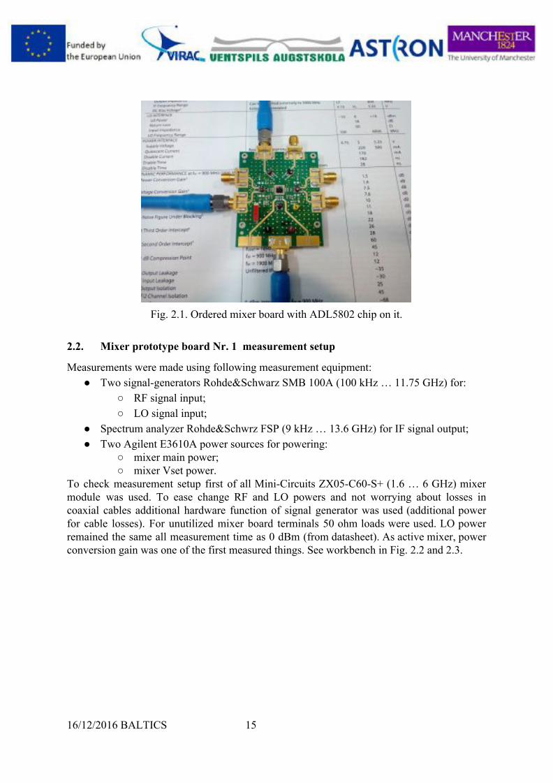
Fig. 2.1. Ordered mixer board with ADL5802 chip on it.
2.2. Mixer prototype board Nr. 1 measurement setup
Measurements were made using following measurement equipment: ● Two signal-generators Rohde&Schwarz SMB 100A (100 kHz … 11.75 GHz) for:
○ RF signal input; ○ LO signal input;
● Spectrum analyzer Rohde&Schwrz FSP (9 kHz … 13.6 GHz) for IF signal output; ● Two Agilent E3610A power sources for powering:
○ mixer main power; ○ mixer Vset power.
To check measurement setup first of all Mini-Circuits ZX05-C60-S+ (1.6 … 6 GHz) mixer module was used. To ease change RF and LO powers and not worrying about losses in coaxial cables additional hardware function of signal generator was used (additional power for cable losses). For unutilized mixer board terminals 50 ohm loads were used. LO power remained the same all measurement time as 0 dBm (from datasheet). As active mixer, power conversion gain was one of the first measured things. See workbench in Fig. 2.2 and 2.3.
16/12/2016 BALTICS 15

Fig. 2.1. Fig. 2.3.
In datasheet at 1.5 GHz for power conversion gain used Vset voltage equals to 5V, Vset = 4.5 V, T(ambient temperature) = 25 degrees, F(LO) = F(RF) - 211 MHz, thereby 1.289 GHz, LO power = 0 dBm, Z0 = 50 ohms. Taking mentioned in account fig. 2.4 shows the result for mixer gain. Power of IF output spectral component is -21.44 dBm at 211 MHz. Approximate signal loss of cable is 1 dBm, the -0.44 dBm is the remained power, what is close value to -0.5 dBm as written in datasheet. Thereby this result is adequate and credible. The next one measurement was input 1 dBm compression point. According to datasheet 1 dBm compression point typical is 13 dbm. Using Vset voltage mixer consumes more current, approximate ~250 mA, when Vs = 5V and Vset 4.5 V. To reduce current, Vset pin can be disconnected. More current improves IP3 and P1dB but degrades SSB NF. Less current degrades IP3 and P1dB but improves SSB NF. Power conversion gain remains nearly the same changing Vset voltage. RF input and IF output powers are shown in fig. 2.5 for IF=211 MHz, but fig. 2.6 represents P1dB curve. Fig. 2.5 shows that when RF reaches input power of 12 dBm, compression starts (difference between two IF powers is only 0.7 dBm).
16/12/2016 BALTICS 16

Fig. 2.4. IF output signal spectral IF component at 211 MHz.
Fig. 2.5. RF input and IF output powers.
16/12/2016 BALTICS 17

Fig. 2.6. P1dB.
Additional curves for IF = 50 MHz and IF = 150 MHz are shown in fig. 2.7 and 2.8. Appropriate output data are shown in Annex 1.3 ( P1dB data for IF at 50 and 150 MHz).
Fig. 2.7. P1dB with IF = 50 MHz.
Fig. 2.8. P1dB with IF = 150 MHz.
16/12/2016 BALTICS 18

2.3. Mixer prototype board Nr. 1 Vset voltage investigation
Investigation of Vset voltage was done to get knowledge about powers of RF and IF spectral components. Eight spectrum fig. (1 to 8) shows IF and RF bands. LO frequency 1.35 GHz 0 dBm, RF 1.4 and 1.5 GHz 7 dBm. Thereby comparison in cases when Vset is 4.5 (I = 250 mA) V or disconnected (I = 180 mA) can be done. For cases when RF = 1.4 GHz and RF = 1.5 GHz with Vset = 4.5 V in IF band only three spectral components can be seen, respectively 50, 150, 200 MHz and 150, 300, 450 MHz. In the same situation but with Vset disconnected, more than three spectral components are visible in IF band. Hence Vset voltage affects spectrum power and undesired components shows up when Vset pin is disconnected. The first downconversion band is from 50 MHz to 150 MHz (LO = 1.35 GHz, RF from 1.4 GHz to 1.5 GHz). So upper frequency bands may contain spectral components from previous bands which are undesirable.
1: IF band. RF = 1.4 GHz (7dBm), LO = 1.35 GHz (0dBm) Vset = 4.5V, Vs = 5.0V
I = 250 mA, Ref = 8 dBm, Averaging 100
2: IF band. RF = 1.4 GHz (7dBm), LO = 1.35 GHz (0dBm) Vset = disconnected, Vs = 5.0V
I = 180 mA, Ref = 8 dBm, Averaging 100
16/12/2016 BALTICS 19

3: IF band. RF = 1.5 GHz (7dBm), LO = 1.35 GHz (0dBm) Vset = 4.5V, Vs = 5.0V
I = 250 mA, Ref = 8 dBm, Averaging 100
4: IF band. RF = 1.5 GHz (7dBm), LO = 1.35 GHz (0dBm) Vset = disconnected, Vs = 5.0V
I = 180 mA, Ref = 8 dBm, Averaging 100
Similar situation can be observed in RF band. In both cases when RF = 1.4 GHz and 1.5 GHz with Vset = 4.5V less spectral components shows up unlike when Vset is disconnected.
5: RF band. RF = 1.4 GHz (7dBm), LO = 1.35 GHz (0dBm) Vset = 4.5V, Vs = 5.0V
I = 250 mA, Ref = 8 dBm, Averaging 100
6: RF band., RF = 1.4 GHz (7dBm), LO = 1.35 GHz (0dBm) Vset = disconnected, Vs = 5.0V
I = 180 mA, Ref = 8 dBm, Averaging 100
16/12/2016 BALTICS 20

7: RF band. RF = 1.5 GHz (7dBm), LO = 1.35 GHz (0dBm) Vset = 4.5V, Vs = 5.0V
I = 250 mA, Ref = 8 dBm, Averaging 100
8: RF band. RF = 1.5 GHz (7dBm), LO = 1.35 GHz (0dBm) Vset = disconnected, Vs = 5.0V
I = 180 mA, Ref = 8 dBm, Averaging 100
2.4. Mixer prototype board Nr. 2
To reduce signal downconversion block expenses, another mixer prototype board was made - mixer prototype board nr. 1. Chosen dielectric is FR4 unlike Rogers type material for board nr. 1 and also board layout differs. Fig. 2.9 shows ADL5802 basic schematic used in prototype board nr. 2. For RF and LO input ports 1:1 impedance transformers (baluns) are used. For IF output 1:4 center tapped baluns are used, because IF ports have 200 ohms differential outputs. Appropriate capacitance capacitors are used, especially filter capacitors for power and for baluns. First class MLCC C0G type capacitors were chosen to provide no change in capacitance over time and voltage, as well negligible change in capacitance with reference to ambient temperature. L1, L2 and L3 are RF1, RF2 and LO baluns, respectively. L4 and L5 are IF center tapped baluns.
16/12/2016 BALTICS 21

Fig. 2.9. ADL5802 basic schematic.
Fig. 2.10 and 2.11 shows board layout, respectively top and bottom layers. In the center of the board ADL5802 mixer is situated with baluns and capacitors around it. In the left side voltage stabiliser provide 5V power for the mixer. SMA edge mount connectors are used for RF, LO inputs and IF outputs. Board thickness is 0.8 mm. Therebay 50 ohm trace which is classified as coplanar waveguide is 1 mm wide if space between trace and ground layer is 0.2 mm. Fig. 2.12 and 2.13 shows board 3D model and soldered prototype board. To test used baluns itself one more dedicated board was manufactured.
16/12/2016 BALTICS 22

Fig. 2.10 Fig. 2.11
Fig. 2.12 Fig. 2.13
2.5. Mixer prototype board Nr. 2 measurement setup
Using network analyzer Agilent Technologies E5071C (100 kHz to 4.5 GHz, KNA series) scattering parameters as S11, S21, S21 phase and S22 were measured. In total following measurement combinations were done:
● LO - IF1, NR-1 and NR2 & LO - IF2, NR-1 and NR-2; ● RF2 - IF1, NR-1 and NR-2 & RF2 - IF2, NR1 and NR-1.
Abbreviation NR-1 and NR-2 are used to described voltage and current setup in measurements. So NR-1: V = 5.0 V, I = 150 mA, Vset disconnected, voltage on Vset pin equals 1.49 V; NR-2: V = 5.0V, I = 230 mA, Vset connected, voltage on Vset pin equals 4.5 V. See measurement and workbench setup in fig. 2.14 and 2.15.
16/12/2016 BALTICS 23

Fig. 2.14 Fig. 2.15
S11 in LO - IF1 and LO - IF2 cases corresponds to LO reflection coefficient and measurement results are comparable with information from datasheet.
Fig. 2.16. Return Loss or S11 according to datesheet for BD2425N5050AHF.
For 1.4 to 1.5 GHz band S11 is equal to -30.75 dB at 1.4 GHz and -28.38 at 1.5 GHz. From fig. 2.16 is seen that around 1.45 GHz S11 equals to -28 dB. So results for resonant frequency is similar. One more thing what can be compared is -10 dB bandwidth. Using measurement data -10.26 dB at 1.86 GHz and -10.00 db at 3.03 GHz made up frequency bandwidth approximately 1.2 GHz. Hence BD25N5050AHF balun can also be used for LO (1.35 GHz in this case). Visual observation of curve in fig. 2.17 gives approximately 1.5 GHz -10 dB bandwidth. Thereby brief conclusion is that results are close enough in range up to 4.5 GHz.
16/12/2016 BALTICS 24

Fig. 2.17.
LO-IF1 and LO-IF2 S11 of LO port shows the same result. Similar comparison can be done with IF baluns of S22 measurements. Measurement sets are:
● LO - IF1 & RF2 - IF2; ● LO - IF2 & RF2 - IF1.
Fig. 2.18.
It is seen that fig. 2.18 and 2.19 as well as 2.20 and 2.21 by pairs shows similar curves. Although used baluns have the same impedance transformer model MABAES0061. But S22 average value (8 measurements) at 45.1 MHz is close to -30 dB and at 158 MHz approximately -21 dB, thereby 0.1 % and 0.79 % of reflection, respectively. That is good result and usable -10 dB bandwidth is up to 517 MH. Available information from datasheet says that usable bandwidth is from 1.0 MHz up to 800 MHz. From measurements at 800
16/12/2016 BALTICS 25

MHz S22 drops down to -6 dB, so approximately 25% of reflection. In summary that is one quarter of delivered power and considered as not usable frequency range.
Fig. 2.19.
Fig. 2.20.
16/12/2016 BALTICS 26

Fig. 2.21.
2.6. Balun test board
Impedance transformer or balun test board was made to measure S11, S21, S21 (phase) and S22 parameters. Board was designed for IF balun MABAES0061 (2 MHz to 800 MHz) and RF (also used for LO) balun BD2425N5050AHF (1.4 to 1.5 GHz). Used measurement equipment was network analyzer Agilent Technologies E5071C (100 kHz to 4.5 GHz, KNA series). Data were stored as S2P files. Board top and bottom layers, and physical prototype as well can be seen in fig. 2.22 to 2.24 correspondingly. For each of the balun there is one RF input and two balanced outputs, where each of the trace is in series with 50 ohm resistor, and terminating with 50 ohm load made up 100 ohm resistance giving 200 ohm differential resistance.
Fig. 2.22. TOP layer Fig. 2.23. BOTTOM layer
16/12/2016 BALTICS 27

Fig. 2.24.
S11, S21, S21 phase and S22 measurements of each are representable in one graph. See fig. 2.24 to 2.48. Ports are marked as RFin, B1out and B2out, where B stands for balanced. Thereby three port combinations are possible for measurements: RFin - B1out, RFin - B2out and B1out - B2out. S11 measurements are port RFin reflection coefficient. In RFin - B1out case at 45.1 MHz -18.91 dB and at 158 MHz -17.61 dB, but for RFin-B2out at 45.1 MHz -18.86 dB and at 158 MHz -17.55. So these two measurements shows very close result of S11.
Fig. 2.25 Reflection coefficient S11.
Datasheet says, that insertion loss in frequency range from 5 - 600 MHz typical is 1.2 dB and maximum value can reach 2 dB and in range from 2 MHz to 800 MHz maximum can reach 3 dB. Looking to fig. 2.26 can be seen that for RFin - B1out and RFin - B2out in range from
16/12/2016 BALTICS 28

45.1 MHz to 158 MHz S21 value is below -5 dB - S21 in this situation is called as attenuation. Specifying:
● RFin - B1out: at 45.1 MHz -6.77 dB and at 158 MHz -6.89 dB; ● RFin - B2out: at 45.1 MHz -6.80 dB and at 158 MHz -6.95 dB.
Fig. 2.26. Insertion loss.
To do clear insertion loss measurement, the first need to measure attenuation of coplanar waveguide itself, and then from S21 measurement, including impedance transformer, subtract coplanar waveguide attenuation. After this operation comparison between information from datasheet can be done. Thereby balun test board need to be complemented with coplanar waveguide (without any parts in this trace). S22 measurements represents reflection coefficients of ports B1out and B2out. Specifying the results:
● RFin - B1out: at 45.1 MHz -13.90 dB and at 158 MHz -13.41 dB; ● RFin - B2out: at 45.1 MHz -13.89 dB and at 158 MHz -13.49 dB.
16/12/2016 BALTICS 29

Fig. 2.27. Reflection coefficient S22.
In comparison between S22 and S11 can be seen that S22 results are worse than S11. Value -13.0 dB to -14.0 dB corresponds from 5,01% down to 3.98%, but in S11 case -17.5 dB to -19.0 dB conforms from 1.77% down to 1.25%. The phase diagram of the balun S21 is shown in the Fig. 2.28. where non-ideality of the outputs can be seen.
Fig. 2.28.
16/12/2016 BALTICS 30

3. Measurements of the SAAM one channel
Measurements were made using following measurement equipment: ● Two RF signal-generators Rohde&Schwarz SMB 100A for:
○ In-band signal generation; ○ RFI signal generation;
● Power splitter 11667A; ● RF signal-generator Marconi Instruments 2031 for LO signal generation; ● Rohde&Schwarz specter analysator 9 kHz .. 13.6 GHz FSP for results observation
and data acquisition; ● Two Agilent E3610A power sources for powering:
○ LNA board; ○ mixer moard.
Fig. 3.1. Workplace setup for SAAM one channel parameters measurement.
The in-band and RFI signal-generators were both connected to power splitter that output was connected to the LNA. LNA was directly connected to the mixer board, that was connected to IF 50..150 MHz filter board. Spectrum analyser was connected to the output of the IF filter. Overall picture of the setup can be seen in the Figure 3.1.
16/12/2016 BALTICS 31

Spectrum analyser (SA) was configured to the frequency band 10..5000 MHz (for most cases), 8001 trace points, RBW = 3 MHz, VBW = 10 MHz. Both In-band and RFI signal-generators (SGIB and SGRI correspondingly) were configured to generate signals with output level of -30 dBm to avoid SMAA signalpath saturation. LO signal-generator (SGLO) was configured to generate LO signal at frequency 1.35 GHz at output power level 0 dBm.
3.1.Measurement of the upper signal generator signal power over the spectra
This measurement was made to establish spectrum analyser and power splitter response to the In-band signal-generator (SGIB) -30 dBm signal. Response later can be used as an calibration information for measurements level equalisation in the case when deeper and more precise analysis of measurements results is needed. Response is shown in the Figures 3.2 and 3.3. Figure 3.2 shows the overall system response to the SGIB signal from SGIB power splitter input.
Table 3.1 Measurement setup
SGIB setup RF Level -30 dBm
Start: 5 MHz Stop: 5000 MHz
SA setup
Start: 10000000 Hz Stop: 5000000000 Hz
Ref Level -35 dBm Level Offset: 0 dBm
Ref Position: 100 % y-Axis: LOG
Level Range: 50 dB Rf Att: 10 dB
RBW: 3000000 Hz VBW: 10000000 Hz
Trace Mode: MAXHOLD Detector: AVERAGE
x-Unit: Hz y-Unit: dBm
Values: 8001 SWT: 0,1 s
16/12/2016 BALTICS 32

Fig. 3.2. The overall system response to the SGIB signal from SGIB power splitter input.
Fig. 3.3. The overall system response to the SGIB signal from SGRI power splitter input.
3.2.Measurement of the system response to weak signal f SGIB=2.4 GHz (-30 dBm, A ) 1
System was measured till mixer output (no IF filter at output) to see overall channel performance for signal not saturating the system (next measurement was made for more powerful -20 dBm signal).
Table 3.2 Measurement setup
SGIB setup RF Level: -30 dBm
RF frequency: 2400 MHz
1 different letters and numbers were used to mark measurement set output folders to keep track of measurements made in different measurement modes mainly to keep ability to quickly find corresponding data
16/12/2016 BALTICS 33

SGRI setup RF Level: off
RF frequency: -
LO setup RF Level: 0 dBm
RF frequency: 2350 MHz
SA setup Average count: 100
Start: 5000000 Hz Stop: 5000000000 Hz
Ref Level -10 dBm Level Offset: 0 dBm
Ref Position: 100 % y-Axis: LOG
Level Range: 100 dB Rf Att: 20 dB
RBW: 3000000 Hz VBW: 10000000 Hz
Trace Mode: AVERAGE Detector: AVERAGE
x-Unit: Hz y-Unit: dBm
Values: 8001 SWT: 0,1 s
Fig. 3.4. The system response to the -30 dBm level signal f SGIB=2.4 GHz.
3.3.Measurement of the system response to signal fSGIB=2.4 GHz (-20 dBm, B)
Table 3.3 Measurement setup
SGIB setup RF Level: -30 dBm
16/12/2016 BALTICS 34

RF frequency: 2400 MHz
SGRI setup RF Level: off
RF frequency: -
LO setup RF Level: 0 dBm
RF frequency: 2350 MHz
SA setup Average count: 100
Start: 5000000 Hz Stop: 5000000000 Hz
Ref Level 0 dBm Level Offset: 0 dBm
Ref Position: 100 % y-Axis: LOG
Level Range: 100 dB Rf Att: 30 dB
RBW: 3000000 Hz VBW: 10000000 Hz
Trace Mode: AVERAGE Detector: AVERAGE
x-Unit: Hz y-Unit: dBm
Values: 8001 SWT: 0,1 s
Fig. 3.5. The system response to the -20 dBm level signal f SGIB=2.4 GHz.
The last two pictures show that for the input signals up to -20 dBm the system is pretty linear since lower order IF products are at noise level, but higher order mixing products should be filtered out with IF filter.
16/12/2016 BALTICS 35

3.4.Measurement of the system response to mirror channel signal fSGIB=2.3 GHz (-20 dBm, C)
Table 3.4 Measurement setup
SGIB setup RF Level: -20 dBm
RF frequency: 2300 MHz
SGRI setup RF Level: off
RF frequency: -
LO setup RF Level: 0 dBm
RF frequency: 2350 MHz
SA setup Average count: 100
Start: 5000000 Hz Stop: 5000000000 Hz
Ref Level 0 dBm Level Offset: 0 dBm
Ref Position: 100 % y-Axis: LOG
Level Range: 100 dB Rf Att: 20 dB
RBW: 3000000 Hz VBW: 10000000 Hz
Trace Mode: AVERAGE Detector: AVERAGE
x-Unit: Hz y-Unit: dBm
Values: 8001 SWT: 0,1 s
16/12/2016 BALTICS 36
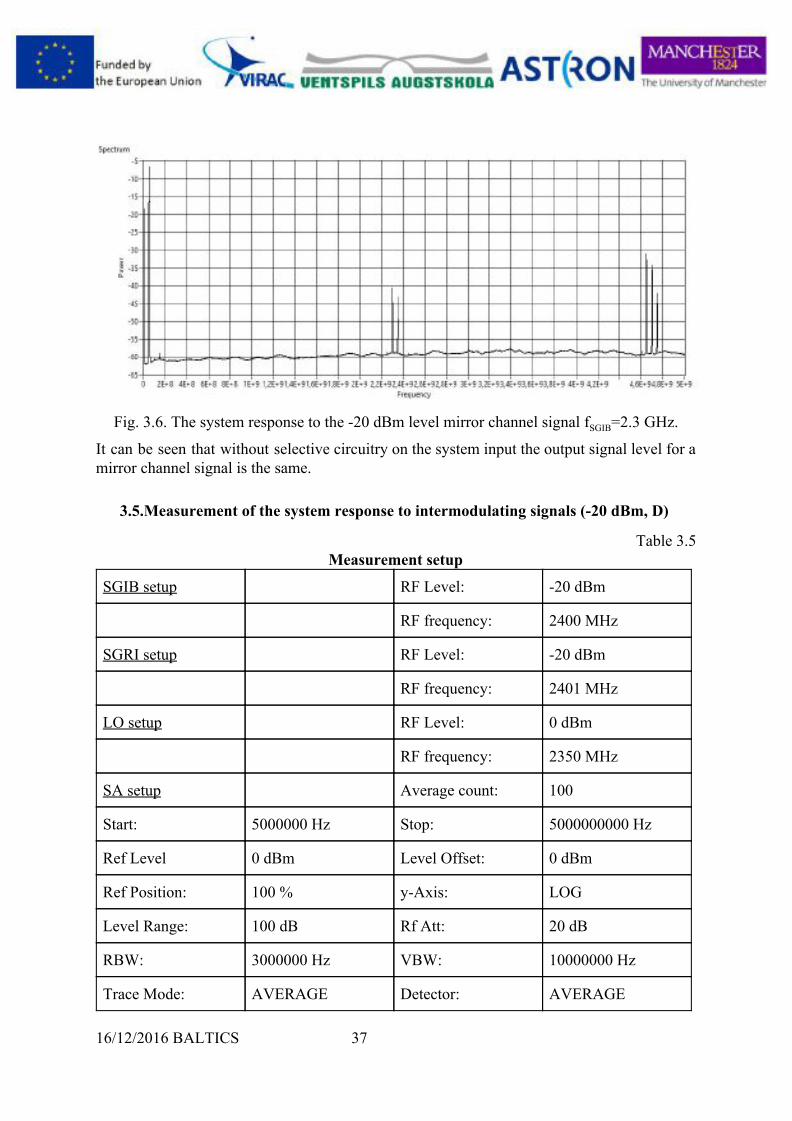
Fig. 3.6. The system response to the -20 dBm level mirror channel signal f SGIB=2.3 GHz.
It can be seen that without selective circuitry on the system input the output signal level for a mirror channel signal is the same.
3.5.Measurement of the system response to intermodulating signals (-20 dBm, D)
Table 3.5 Measurement setup
SGIB setup RF Level: -20 dBm
RF frequency: 2400 MHz
SGRI setup RF Level: -20 dBm
RF frequency: 2401 MHz
LO setup RF Level: 0 dBm
RF frequency: 2350 MHz
SA setup Average count: 100
Start: 5000000 Hz Stop: 5000000000 Hz
Ref Level 0 dBm Level Offset: 0 dBm
Ref Position: 100 % y-Axis: LOG
Level Range: 100 dB Rf Att: 20 dB
RBW: 3000000 Hz VBW: 10000000 Hz
Trace Mode: AVERAGE Detector: AVERAGE
16/12/2016 BALTICS 37

x-Unit: Hz y-Unit: dBm
Values: 8001 SWT: 0,1 s
Fig. 3.7. The system response to the -20 dBm level intermodulating signals.
In this case lower order mixing products are more powerful. It indicates that for -20 dBm level input signals the noise level rises for some 10 dB that is caused by intermodulation of the input signals..
3.6.Measurement of the filtered system response to signal fSGIB=2.4 GHz (-20 dBm, G)
Table 3.6 Measurement setup
SGIB setup RF Level: -20 dBm
RF frequency: 2400 MHz
SGRI setup RF Level: off
RF frequency: -
LO setup RF Level: 0 dBm
RF frequency: 2350 MHz
SA setup Average count: 100
Start: 5000000 Hz Stop: 5000000000 Hz
Ref Level 0 dBm Level Offset: 0 dBm
Ref Position: 100 % y-Axis: LOG
16/12/2016 BALTICS 38

Level Range: 100 dB Rf Att: 30 dB
RBW: 3000000 Hz VBW: 10000000 Hz
Trace Mode: AVERAGE Detector: AVERAGE
x-Unit: Hz y-Unit: dBm
Values: 8001 SWT: 0,1 s
Fig. 3.8. The system response to the -20 dBm level signal f SGIB=2.4 GHz.
It can be seen that the seventh order IF filter effectively filters out higher order IF components but lower order IF harmonics (second and third) are around the system’s noise level -60 dBm. The measured lower order mixing product levels are shown in following table.
Level at system output IF = 50 MHz IF2 = 100 MHz IF3 = 150 MHz
without IF filter, dBm -7,23 -59,76 -59,19
with IF filter, dBm -15,88 -60,22 -59,87
3.7.Mixing products measurement (no IF filter) at f SGIB=2.5 GHz (-20 dBm, I)
This measurement was made to see the mixing products at the output of the mixer for different input signal that will have different (three times more) frequency output IF signal. The unfiltered and filtered mixing products comparison will show efficiency of the designed IF filter.
Table 3.7 Measurement setup
SGIB setup RF Level: -20 dBm
16/12/2016 BALTICS 39

RF frequency: 2500 MHz
SGRI setup RF Level: off
RF frequency: -
LO setup RF Level: 0 dBm
RF frequency: 2500 MHz
SA setup
Start: 5 MHz Stop: 5000 MHz
Ref Level 0 dBm Level Offset: 0 dBm
Ref Position: 100 % y-Axis: LOG
Level Range: 100 dB Rf Att: 30 dB
RBW: 3000000 Hz VBW: 10000000 Hz
Trace Mode: MAXHOLD Detector: AVERAGE
x-Unit: Hz y-Unit: dBm
Values: 8001 SWT: 0,1 s
Fig. 3.9. The system response to the -20 dBm level signal f SGIB=2.5 GHz.
It can be seen that lower order IF components are at system’s noise level, but higher order mixing products demand filtering.
16/12/2016 BALTICS 40

3.8.Measurement of the filtered system response to signal fSGIB=2.5 GHz (-20 dBm, H)
Table 3.8 Measurement setup
SGIB setup RF Level: -20 dBm
RF frequency: 2500 MHz
SGRI setup RF Level: off
RF frequency: -
LO setup RF Level: 0 dBm
RF frequency: 2350 MHz
SA setup Average count: 100
Start: 5000000 Hz Stop: 5000000000 Hz
Ref Level 0 dBm Level Offset: 0 dBm
Ref Position: 100 % y-Axis: LOG
Level Range: 100 dB Rf Att: 30 dB
RBW: 3000000 Hz VBW: 10000000 Hz
Trace Mode: AVERAGE Detector: AVERAGE
x-Unit: Hz y-Unit: dBm
Values: 8001 SWT: 0,1 s
16/12/2016 BALTICS 41

Fig. 3.10. The system response to the -20 dBm level signal f SGIB=2.5 GHz.
Measurement shows that the designed seventh order IF filter filters out all parasitic mixing components. Lower order IF component level measurements are shown in a following table.
Level at system output IF = 150 MHz IF2 = 300 MHz IF3 = 450 MHz
without IF filter, dBm -7,62 -59,66 -59,88
with IF filter, dBm -10,27 - -
3.9. Measurement of the complete system at f SGIB=1.8 GHz (-20 dBm, J)
Measurement was made to see RFI influence onto the system. Averaging was chosen equal to 1000 to do not lose signal in noise.
Table 3.9 Measurement setup
SGIB setup RF Level: -20 dBm
RF frequency: 1800 MHz
SGRI setup RF Level: off
RF frequency: -
LO setup RF Level: 0 dBm
RF frequency: 2350 MHz
SA setup Average count: 1000
Start: 5000000 Hz Stop: 5000000000 Hz
16/12/2016 BALTICS 42

Ref Level 0 dBm Level Offset: 0 dBm
Ref Position: 100 % y-Axis: LOG
Level Range: 100 dB Rf Att: 30 dB
RBW: 3000000 Hz VBW: 10000000 Hz
Trace Mode: AVERAGE Detector: AVERAGE
x-Unit: Hz y-Unit: dBm
Values: 8001 SWT: 0,1 s
Fig. 3.11. The system response to the -20 dBm level RFI signal fSGIB=1.8 GHz.
RFI signal fSGIB=1.8 GHz after filter can not be observable. It means that signal is or at system’s noise level, or below it.
3.10. Measurement of the complete system at f SGIB=1.14 GHz (-20 dBm, K)
In this case system was measured to see response to another RFI signal at frequency 1.14 GHz.
Table 3.10 Measurement setup
SGIB setup RF Level: -20 dBm
RF frequency: 1140 MHz
SGRI setup RF Level: off
RF frequency: -
16/12/2016 BALTICS 43

LO setup RF Level: 0 dBm
RF frequency: 2350 MHz
SA setup Average count: 1000
Start: 5000000 Hz Stop: 5000000000 Hz
Ref Level 0 dBm Level Offset: 0 dBm
Ref Position: 100 % y-Axis: LOG
Level Range: 100 dB Rf Att: 30 dB
RBW: 3000000 Hz VBW: 10000000 Hz
Trace Mode: AVERAGE Detector: AVERAGE
x-Unit: Hz y-Unit: dBm
Values: 8001 SWT: 0,1 s
Fig. 3.12. The system response to the -20 dBm level RFI signal fSGIB=1.14 GHz.
On the output of the system RFI signal can not be observed. Instead the parasitic IF signal with frequency 70 MHz and level about -55 dBm can be observed. It means the system should have some selective circuitry before or after LNA.
3.11. Measurement of the complete system at f SGIB=0.9 GHz (-20 dBm, L)
Next was measured system response onto the RFI signal with frequency 0.9 GHz (interference from mobile phone stations).
16/12/2016 BALTICS 44

Table 3.11 Measurement setup
SGIB setup RF Level: -20 dBm
RF frequency: 1140 MHz
SGRI setup RF Level: off
RF frequency: -
LO setup RF Level: 0 dBm
RF frequency: 2350 MHz
SA setup Average count: 1000
Start: 5000000 Hz Stop: 5000000000 Hz
Ref Level -10 dBm Level Offset: 0 dBm
Ref Position: 100 % y-Axis: LOG
Level Range: 100 dB Rf Att: 20 dB
RBW: 3000000 Hz VBW: 10000000 Hz
Trace Mode: AVERAGE Detector: AVERAGE
x-Unit: Hz y-Unit: dBm
Values: 8001 SWT: 0,1 s
Fig. 3.13. The system response to the -20 dBm level RFI signal fSGIB=0.9 GHz.
16/12/2016 BALTICS 45

On the output of the system the RFI signal is not observable. Instead was observed an SA nonlinearity. To avoid impact from this nonlinearity measurements were continued with setting Ref Level >= -10 dBm.
3.12. Measurement of the complete system at f SGIB=1550..3450 MHz (-20 dBm, O)
To observe system response to input signals with different frequency, an input signal sweep was used.
Table 3.12 Measurement setup
SGIB setup RF Level: -20 dBm
RF frequency: 1140 MHz
SGRI setup RF Level: off
RF frequency: -
LO setup RF Level: 0 dBm
RF frequency: 2350 MHz
SA setup Average count: 1000
Start: 5000000 Hz Stop: 5000000000 Hz
Ref Level 0 dBm Level Offset: 0 dBm
Ref Position: 100 % y-Axis: LOG
Level Range: 100 dB Rf Att: 20 dB
RBW: 3000000 Hz VBW: 10000000 Hz
Trace Mode: MAXHOLD Detector: AVERAGE
x-Unit: Hz y-Unit: dBm
Values: 8001 SWT: 0,1 s
16/12/2016 BALTICS 46

Fig. 3.14. The system response to the -20 dBm level signals fSGIB=1.55..3.45 GHz.
Main response maximum is observable in the frequency region 50..150 MHz that corresponds to the main system IF signals. It can be seen that filtering capabilities of the IF filter for signals above 2 GHz are less. To avoid this a better quality (high frequency) components for filter should be used.
3.13. Measurement of the complete system at f SGIB=175..550 MHz (-20 dBm, S)
Measurement was made to check system response on RFI signals in frequency range 175..550 MHz.
Table 3.13 Measurement setup
SGIB setup RF Level: -20 dBm
RF frequency: 1140 MHz
SGRI setup RF Level: off
RF frequency: -
LO setup RF Level: 0 dBm
RF frequency: 2350 MHz
SA setup Average count: 1000
Start: 5000000 Hz Stop: 5000000000 Hz
Ref Level 0 dBm Level Offset: 0 dBm
Ref Position: 100 % y-Axis: LOG
Level Range: 100 dB Rf Att: 20 dB
16/12/2016 BALTICS 47

RBW: 3000000 Hz VBW: 10000000 Hz
Trace Mode: MAXHOLD Detector: AVERAGE
x-Unit: Hz y-Unit: dBm
Values: 8001 SWT: 0,1 s
Fig. 3.15. The system response to the -20 dBm level RFI signals f SGIB=175..550 MHz.
Measurement shows the real noise level around -55 dBm of the system that includes systems noises and RFI impact onto the sensitivity of the system.
16/12/2016 BALTICS 48