polymer-mems-based optoelectronic display · polymer-mems-based optoelectronic display ... ali...
TRANSCRIPT
IEEE TRANSACTIONS ON ELECTRON DEVICES, VOL. 57, NO. 1, JANUARY 2010 145
Polymer-MEMS-Based Optoelectronic DisplayY. Daghan Gokdel, Student Member, IEEE, Ali Osman Sevim,
Senol Mutlu, Member, IEEE, and Arda D. Yalcinkaya, Member, IEEE
Abstract—In this paper, a novel all-polymer integrated mi-crosystem, which realizes a 2-D display by integrating a 1-Darray of polymer light-emitting diodes (PLEDs) with a poly-mer scanner of microelectromechanical system (MEMS), ispresented. Electronic modulation of PLEDs forms the first di-mension of the display (fast scan), and the scanner actuationorthogonal to the direction of PLED lineup forms the secondone (slow scan). MEMS scanner (actuator) is fabricated on apolymer composite (FR4 material) with a double-sided processusing lithography to pattern copper lines and laser micromachin-ing to cut the scanner outline. PLEDs are fabricated on poly-ethylene terephthalate sheets. They have a thin-film structure ofindium tin oxide, poly (3,4-ethylenedioxythiophene) poly (styre-nesulfonate), poly [2-methoxy-5-(2′-ethyl-hexyloxy)-1,4-phenylenevinylene], and aluminum. The scanner is actuated electromag-netically in its slow-scan resonance mode at 49 Hz, generating amaximum displacement of 3.5 mm at a drive power of 84 mWwith the help of a mini permanent magnet attached to the tipof the scanner and an off-chip energizing coil. Turn-on voltageof a PLED is 7.5 V, and each one generate a luminance of0.3 cd/m2 at 13 V, consuming 1.1-mA current. Successful operationof the integrated-display system is shown by forming a checker boximage with a resolution of 20 × 7 and a size of 9 mm by 3.4 mm.
Index Terms—Display, MOEMS, polymer integrated microsys-tem, polymer light-emitting diodes (PLEDs).
I. INTRODUCTION
INTEGRATION of polymer microelectromechanical sys-tems (MEMS) with polymer light-emitting diodes (PLEDs)
in order to produce 2-D displays is an attractive solution.There are a number of studies of semiconductor LED-baseddot matrix displays, which are currently known to be a maturetechnology [1]–[3]. These conventional solutions incorporatemodulation of 2-D LED matrix with a driver electronic circuitry[4], [5]. Resolution of such a display depends on the number ofLEDs in the 2-D matrix, which becomes excessively large interms of device count and expensive for high-resolution sys-tems. Such a conventional realization technique for 2-D matrixdisplays not only suffers from the large number of LEDs usedin the system but also the following conditions: 1) low yielddue to difficulties in high-density semiconductor optoelectronicdevice fabrication; 2) reliability problems (dead pixels, LED-to-
Manuscript received May 20, 2009; revised September 25, 2009. Currentversion published December 23, 2009. This work was supported by theScientific and Technological Research Council of Turkey TUBITAK underProjects 107E053 and 106E013. The review of this paper was arranged byEditor L. Lunardi.
The authors are with the Electrical and Electronics Engineering Depart-ment, Bogazici University, Istanbul 34342, Turkey (e-mail: [email protected]).
Color versions of one or more of the figures in this paper are available onlineat http://ieeexplore.ieee.org.
Digital Object Identifier 10.1109/TED.2009.2034507
LED variations in luminance–current characteristics, etc.); and3) high power consumption of the LED matrix.
Present system offers a novel method for realization of 2-Ddisplays by integrating the light sources (PLED) with theMEMS actuators. The operation of the system relies on themodulation of the light sources in one axis (called fast-scanaxis) and the resonant movement of the LED-integrated MEMSplatform in the axis perpendicular to the fast-scan axis (calledslow-scan axis). This method has a number of novelties overthe conventional techniques, such as the following: 1) usageof only one row of PLED array leads to severe reductionin the cost of light sources; 2) due to reduced number oflight sources, reliability is expected to increase significantly,having much smaller number of dead pixels and lower amountof LED-to-LED variation (depending on the resolution, thisenhancement is expected to be around the number of rows);3) power consumption of the 2-D display proposed in this paperis the sum of the powers consumed by the 1-D LED array andthe MEMS actuator, which is much smaller than the power con-sumption of 2-D LED matrix displays; 4) the present displayrepresents a technologically new class, and it is, in principal,possible to perform full monolithic integration with polymerPLEDs; 5) traditional LED-based 2-D displays, excluding or-ganic and/or polymer LEDs and electronics, cannot use activematrix addressing and are limited to passive matrix addressing[1], which in turn puts limitations on the resolution and size ofthe displays. Present method, however, alleviates this problemsignificantly, due to 1-D array addressing simplicity, even if thepassive array addressing is used. This interdisciplinary studyclaims to yield in a highly original 2-D display, merging twohigh-tech fields, namely, the MEMS and polymer electrooptics.There is no similar system previously reported in the litera-ture that enables the integration of polymer MEMS actuatorswith PLEDs to implement medium-resolution, e.g., QVGA(320 × 256), VGA (640 × 512) miniaturized 2-D displays.Representative numbers for a potential VGA realization are asfollows: a LED emitter size of 50 μm × 50 μm, a LED pitch of100 μm, and an actuator width of 65 mm. These numbers showthat it is realistic to have a display in a common video format.Such a display component can be used in consumer electronicsproducts (mobile phones, MP3 players, digital cameras, hand-held PDAs, etc.), representing an alternative class of display asa reliable, robust, low-power, and low-cost system.
This paper is organized as follows. Section II describesthe device operation where the display subsystems, namely, amagnetic actuator, and PLED principles are given. Section IIIis devoted to the fabrication and integration of the subsystemsto implement a display. Following, Section IV discusses theperformance of the implemented system. Concluding remarksand outlook are supplied in Section V.
0018-9383/$26.00 © 2009 IEEE
Authorized licensed use limited to: ULAKBIM UASL - BOGAZICI UNIVERSITESI. Downloaded on January 6, 2010 at 03:53 from IEEE Xplore. Restrictions apply.
146 IEEE TRANSACTIONS ON ELECTRON DEVICES, VOL. 57, NO. 1, JANUARY 2010
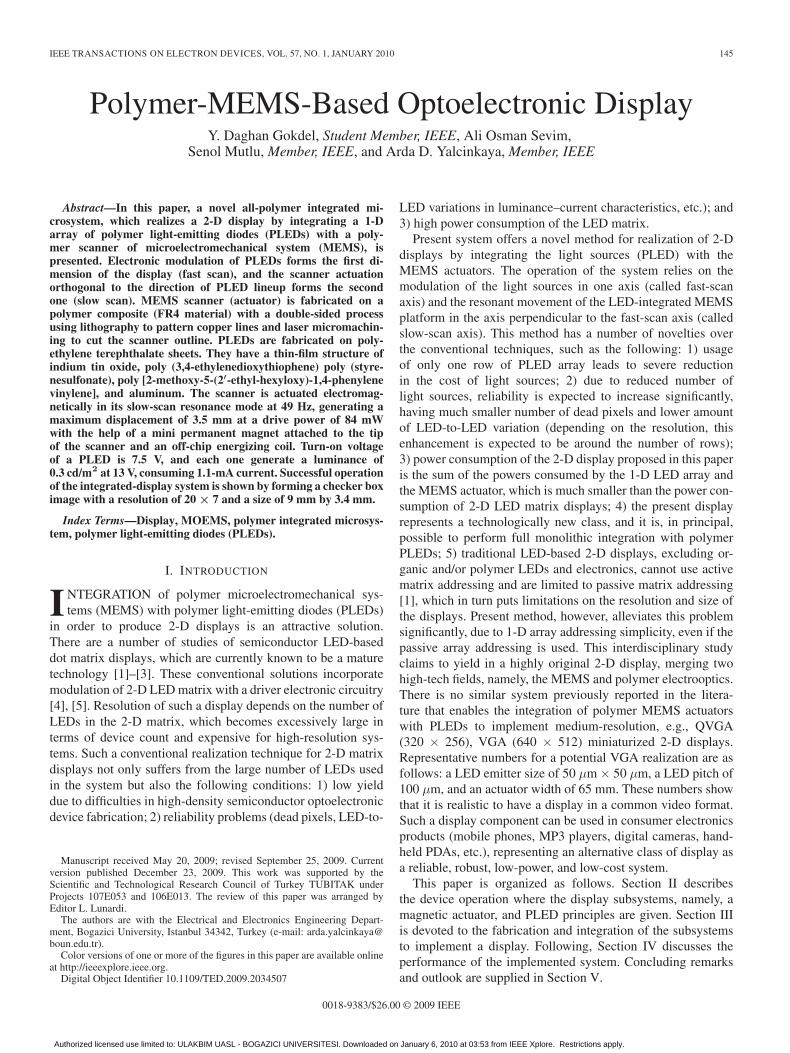
Fig. 1. (a) Schematic of the polymer-based MEMS display. (b) Electronic-modulation and MEMS-actuation directions.
II. DEVICE OPERATION
A. MEMS Actuator
Schematic of the proposed system that uses a novel methodfor realization of 2-D displays by integrating 1-D array of lightsources (LEDs) with a MEMS actuator is shown in Fig. 1(a),where an actuator suspended with two springs at the anchoringregions and an array of PLEDs placed on the actuator surfacecan be identified. Basic operation of the device relies on theelectronic modulation of the light sources in the fast-scan axisand the mechanical vibration of the actuator at a designedfrequency (refresh rate) in the slow-scan axis, as shown inFig. 1(b). Simultaneous control of the slow-scan movement ofthe MEMS actuator and the electronic modulation of the LEDsform virtual pixels and thus generate a 2-D image, as enclosedby the 2-D image plane in Fig. 1(b).
The slow-scan motion of this scanning display is realizedby electromagnetic actuation of the FR4 structure at its fun-damental resonant mode. The MEMS actuator defines both therefresh rate and the resolution of the 2-D image; therefore, it isimportant to have a reasonable refresh rate (e.g., 50 Hz) as wellas a large shuttle deflection. The actuator used in this paper canbe pictured as a combination of two cantilevers and a lumpedshuttle mass. Resonance frequency related to the out-of-planemovement of the actuator can be approximated as
f =1
2π
√2k
mL + meff(1)
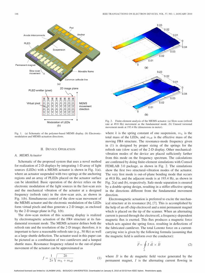
Fig. 2. Finite-element analysis of the MEMS actuator. (a) Slow-scan (refreshrate at 49.8 Hz) movement as the fundamental mode. (b) Unused torsionalmovement mode at 193.4 Hz (dimensions in meter).
where k is the spring constant of one suspension, mL is thetotal mass of the LEDs, and meff is the effective mass of themoving FR4 structure. The resonance-mode frequency givenin (1) is designed by proper sizing of the springs for therefresh rate (slow scan) of the 2-D display. Other mechanical-vibration modes of the device are placed sufficiently fartherfrom this mode on the frequency spectrum. The calculationsare confirmed by doing finite-element simulations with ComsolFEMLAB 3.0 package, as shown in Fig. 2. The simulationsshow the first two structural-vibration modes of the actuator.The very first mode is out-of-plane bending mode that occursat 49.8 Hz, and the adjacent mode is at 193.4 Hz, as shown inFig. 2(a) and (b), respectively. Safe-mode separation is ensuredby a double-spring design, resulting in a stiffer effective springin the directions different from the fundamental movementdirection.
Electromagnetic actuation is preferred to excite the mechan-ical structure at its resonance [6], [7]. This is accomplished bythe help of an off-chip electrocoil and a mini permanent magnetwhich is placed on the tip of the scanner. When an alternatingcurrent is passed through the electrocoil, a frequency-dependentmagnetic flux is exerted. This flux produces a magnetic forcewhich acts against the spring force, resulting in deflections ofthe fabricated cantilever. The total Lorentz force on a current-carrying wire is given by the following formula (assuming thatthe magnetic field is uniform over the conductor):
→F=
∮L
I→dl ×
→B (2)
where B is the dc magnetic field vector generated by thepermanent magnet, I is the alternating current flowing in
Authorized licensed use limited to: ULAKBIM UASL - BOGAZICI UNIVERSITESI. Downloaded on January 6, 2010 at 03:53 from IEEE Xplore. Restrictions apply.
GOKDEL et al.: POLYMER-MEMS-BASED OPTOELECTRONIC DISPLAY 147
the electrocoil, and L is the effective length of the current-carrying conductor [8]. Since off-chip coils offer much longerconductor lengths than the coils implemented on the chip, it ismore advantageous to use off-chip coil and on-chip permanentmagnet to maximize the actuation force. When the frequency ofthe actuation force enters into the passband of the mechanicalresonator, the movable frame displacement increases drasticallydue to high mechanical quality factor of the scanner. Mechan-ical actuator acts like a passive filter with high quality factor,converting the displacements near the resonance frequenciesto higher excursions. This effect helps to decrease the powerconsumption of the MEMS driver to the range of a few milli-watts. Since there are a number of mechanical modes occurringat different distinct frequencies, the scanner is driven only atthe specific slow-scan mode by using a sinusoidal signal sourceat the out-of-plane bending resonance-peak frequency. Spectralpurity of the driving electrical signal becomes important be-cause it can excite other modes which can appear as parasiticmotions to the fundamental one.
B. PLEDs
Conjugated polymers are semiconductors that offer flexi-bility, simplicity, and lower cost in the fabrication of LEDs[9], transistors [10], integrated circuits [11], photodetectors,and solar cells [12]. Their usage has a potential to realizemonolithic integration of electronic, optoelectronic, MEMS,and sensory devices [13] altogether. In addition, polymer-basedsystems are amenable to roll-to-roll production [14]. How-ever, when compared to their inorganic counterparts, currentpolymer semiconductor devices have lower performances, areless reliable, and have shorter lifetimes due to rapid degrada-tion on exposure to oxygen and water vapor under ambientatmosphere [15].
In this paper, 1-D PLED array is made with a structureof indium tin oxide (ITO), poly (3,4-ethylenedioxythiophene)poly (styrenesulfonate) (PEDOT:PSS), poly [2-methoxy-5-(2′-ethyl-hexyloxy)-1,4-phenylene vinylene] (MEH-PPV), andaluminum (Al). ITO forms a transparent anode electrode.PEDOT-PSS works as a hole-transporting layer. MEH-PPVis the light-emitting layer. Aluminum is used as a low-work-function anode material. Electrons injected from Al and holesfrom ITO recombine on MEH-PPV to emit photons.
In contrast to typical fabrication process in literature, fab-rication of the 1-D PLED array is performed under standardroom conditions without using glove boxes. Therefore, duringeach fabrication step, the polymer materials are degraded byhumidity and oxygen in the environment. As a result, fabricatedPLEDs do not emit light when forward biased. To remedy thissituation, a novel two-step postfabrication-treatment method,consisting of thermal and electric field treatments, is used torevive them [15]. Treatments are done on a hotplate inside avacuum chamber with in situ packaging capability after theelectrical wiring of the array is done. The PLED array ispackaged with a millimeter-thick layer of a hot-melt siliconeimmediately after treatment without breaking vacuum. Thermaltreatment restores the electroluminescent function of PLEDsby removing most of the oxygen and water vapors absorbed
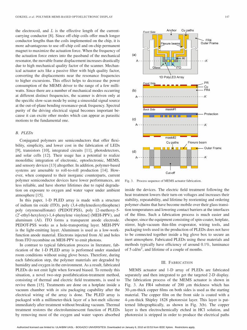
Fig. 3. Process sequence of MEMS actuator fabrication.
inside the devices. The electric field treatment following theheat treatment lowers their turn-on voltages and increases theirstability, repeatability, and lifetime by reorienting and orderingpolymer chains that have become mobile over their glass transi-tion temperatures and lowering contact barriers at the interfacesof the films. Such a fabrication process is much easier andcheaper, since the equipment consisting of spin-coater, hotplate,stirrer, high-vacuum thin-film evaporator, wiring tools, andpackaging tools used in the production of PLEDs does not haveto be connected together inside a big glove box to secure aninert atmosphere. Fabricated PLEDs using these materials andmethods typically have efficiency of around 0.1%, luminanceof 5 cd/m2, and lifetime of a couple of months.
III. FABRICATION
MEMS actuator and 1-D array of PLEDs are fabricatedseparately and then integrated to get the targeted 2-D display.The fabrication process of the MEMS actuator is shown inFig. 3. An FR4 substrate of 200 μm thickness which has30-μm-thick copper films on both sides is used as the startingmaterial. The copper film on the front side is coated with a4-μm-thick Shipley 1828 photoresist layer. This layer is pat-terned lithographically, as shown in Fig. 3(b). The copperlayer is then electrochemically etched in HCl solution, andphotoresist is stripped in order to produce the electrical paths
Authorized licensed use limited to: ULAKBIM UASL - BOGAZICI UNIVERSITESI. Downloaded on January 6, 2010 at 03:53 from IEEE Xplore. Restrictions apply.
148 IEEE TRANSACTIONS ON ELECTRON DEVICES, VOL. 57, NO. 1, JANUARY 2010
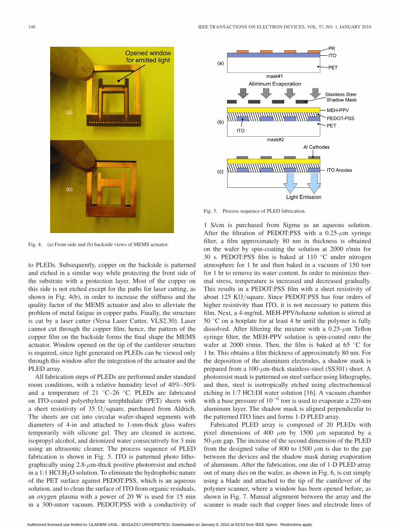
Fig. 4. (a) Front-side and (b) backside views of MEMS actuator.
to PLEDs. Subsequently, copper on the backside is patternedand etched in a similar way while protecting the front side ofthe substrate with a protection layer. Most of the copper onthis side is not etched except for the paths for laser cutting, asshown in Fig. 4(b), in order to increase the stiffness and thequality factor of the MEMS actuator and also to alleviate theproblem of metal fatigue in copper paths. Finally, the structureis cut by a laser cutter (Versa Laser Cutter, VLS2.30). Lasercannot cut through the copper film; hence, the pattern of thecopper film on the backside forms the final shape the MEMSactuator. Window opened on the tip of the cantilever structureis required, since light generated on PLEDs can be viewed onlythrough this window after the integration of the actuator and thePLED array.
All fabrication steps of PLEDs are performed under standardroom conditions, with a relative humidity level of 40%–50%and a temperature of 21 ◦C–26 ◦C. PLEDs are fabricatedon ITO-coated polyethylene terephthalate (PET) sheets witha sheet resistivity of 35 Ω/square, purchased from Aldrich.The sheets are cut into circular wafer-shaped segments withdiameters of 4-in and attached to 1-mm-thick glass waferstemporarily with silicone gel. They are cleaned in acetone,isopropyl alcohol, and deionized water consecutively for 3 minusing an ultrasonic cleaner. The process sequence of PLEDfabrication is shown in Fig. 5. ITO is patterned photo litho-graphically using 2.8-μm-thick positive photoresist and etchedin a 1:1 HCl:H2O solution. To eliminate the hydrophobic natureof the PET surface against PEDOT:PSS, which is an aqueoussolution, and to clean the surface of ITO from organic residuals,an oxygen plasma with a power of 20 W is used for 15 minin a 300-mtorr vacuum. PEDOT:PSS with a conductivity of
Fig. 5. Process sequence of PLED fabrication.
1 S/cm is purchased from Sigma as an aqueous solution.After the filtration of PEDOT:PSS with a 0.25-μm syringefilter, a film approximately 80 nm in thickness is obtainedon the wafer by spin-coating the solution at 2000 r/min for30 s. PEDOT:PSS film is baked at 110 ◦C under nitrogenatmosphere for 1 hr and then baked in a vacuum of 150 torrfor 1 hr to remove its water content. In order to minimize ther-mal stress, temperature is increased and decreased gradually.This results in a PEDOT:PSS film with a sheet resistivity ofabout 125 KΩ/square. Since PEDOT:PSS has four orders ofhigher resistivity than ITO, it is not necessary to pattern thisfilm. Next, a 4-mg/mL MEH-PPV/toluene solution is stirred at50 ◦C on a hotplate for at least 4 hr until the polymer is fullydissolved. After filtering the mixture with a 0.25-μm Teflonsyringe filter, the MEH-PPV solution is spin-coated onto thewafer at 2000 r/min. Then, the film is baked at 65 ◦C for1 hr. This obtains a film thickness of approximately 80 nm. Forthe deposition of the aluminum electrodes, a shadow mask isprepared from a 100-μm-thick stainless-steel (SS301) sheet. Aphotoresist mask is patterned on steel surface using lithography,and then, steel is isotropically etched using electrochemicaletching in 1:7 HCl:DI water solution [16]. A vacuum chamberwith a base pressure of 10−6 torr is used to evaporate a 220-nmaluminum layer. The shadow mask is aligned perpendicular tothe patterned ITO lines and forms 1-D PLED array.
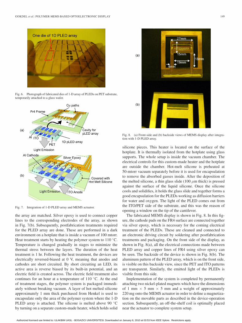
Fabricated PLED array is composed of 20 PLEDs withpixel dimensions of 400 μm by 1500 μm separated by a50-μm gap. The increase of the second dimension of the PLEDfrom the designed value of 800 to 1500 μm is due to the gapbetween the devices and the shadow mask during evaporationof aluminum. After the fabrication, one die of 1-D PLED arrayout of many dies on the wafer, as shown in Fig. 6, is cut simplyusing a blade and attached to the tip of the cantilever of thepolymer scanner, where a window has been opened before, asshown in Fig. 7. Manual alignment between the array and thescanner is made such that copper lines and electrode lines of
Authorized licensed use limited to: ULAKBIM UASL - BOGAZICI UNIVERSITESI. Downloaded on January 6, 2010 at 03:53 from IEEE Xplore. Restrictions apply.
GOKDEL et al.: POLYMER-MEMS-BASED OPTOELECTRONIC DISPLAY 149
Fig. 6. Photograph of fabricated dies of 1-D array of PLEDs on PET substrate,temporarily attached to a glass wafer.
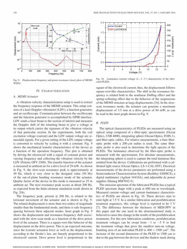
Fig. 7. Integration of 1-D PLED array and MEMS actuator.
the array are matched. Silver epoxy is used to connect copperlines to the corresponding electrodes of the array, as shownin Fig. 7(b). Subsequently, postfabrication treatments requiredfor the PLED array are done. These are performed in a darkenvironment on a hotplate that is inside a vacuum of 100 mtorr.Heat treatment starts by heating the polymer system to 110 ◦C.Temperature is changed gradually in stages to minimize thethermal stress between the layers. The duration of the heattreatment is 1 hr. Following the heat treatment, the devices areelectrically reversed-biased at 0 V, meaning that anodes andcathodes are short circuited. By short circuiting an LED, itsactive area is reverse biased by its built-in potential, and anelectric field is created across. The electric field treatment alsocontinues for an hour at a temperature of 110 ◦C. At the endof treatment stages, the polymer system is packaged immedi-ately without breaking vacuum. A layer of hot melted siliconeapproximately 1 mm thick purchased from Henkel is used toencapsulate only the area of the polymer system where the 1-DPLED array is attached. The silicone is melted above 90 ◦Cby turning on a separate custom-made heater, which holds solid
Fig. 8. (a) Front-side and (b) backside views of MEMS display after integra-tion with 1-D PLED array.
silicone pieces. This heater is located on the surface of thehotplate. It is thermally isolated from the hotplate using glasssupports. The whole setup is inside the vacuum chamber. Theelectrical controls for this custom-made heater and the hotplateare outside the chamber. Hot-melt silicone is preheated at50-mtorr vacuum separately before it is used for encapsulationto remove the absorbed gasses inside. After the deposition ofthe melted silicone, a thin glass slide (100 μm thick) is pressedagainst the surface of the liquid silicone. Once the siliconecools and solidifies, it holds the glass slide and together forms agood encapsulation for the PLEDs working as diffusion barriersfor water and oxygen. The light of the PLED comes out fromthe ITO/PET side of the substrate, and this was the reason ofopening a window on the tip of the cantilever.
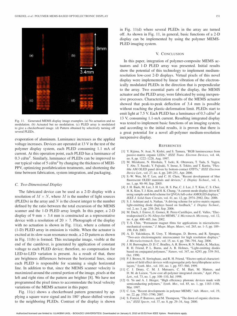
The fabricated MEMS display is shown in Fig. 8. In this fig-ure, the cathode pads on the FR4 surface are connected togethervia silver epoxy, which is necessary for the coming electricaltreatment of the PLEDs. These are cleaned and connected toan electronic driving circuit by soldering after postfabricationtreatments and packaging. On the front side of the display, asshown in Fig. 8(a), all the electrical connections made betweenPLED array and copper lines of FR4 using silver epoxy canbe seen. The backside of the device is shown in Fig. 8(b). Thealuminum pattern of the PLED array, which is on the front side,is visible on this backside view, since the PET and ITO patternsare transparent. Similarly, the emitted light of the PLEDs isvisible from this side.
Implementation of the system is completed by permanentlyattaching two nickel-plated magnets which have the dimensionsof 1 mm × 5 mm × 5 mm and a weight of approximately220 mg onto the MEMS actuator in order to define a magnetiza-tion on the movable parts as described in the device-operationsection. Subsequently, an off-the-shelf coil is optimally placednear the actuator to complete system setup.
Authorized licensed use limited to: ULAKBIM UASL - BOGAZICI UNIVERSITESI. Downloaded on January 6, 2010 at 03:53 from IEEE Xplore. Restrictions apply.
150 IEEE TRANSACTIONS ON ELECTRON DEVICES, VOL. 57, NO. 1, JANUARY 2010
Fig. 9. Displacement-frequency and power-resonance (inset) plots of MEMSdisplay.
IV. CHARACTERIZATION
A. MEMS Actuator
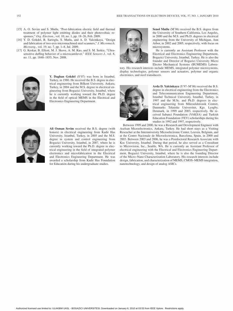
A vibration-velocity characterization setup is used to extractthe frequency response of the MEMS actuator. This setup con-sists of a laser Doppler vibrometer (LDV), a function generator,and an oscilloscope. Communication between the oscilloscopeand the function generator is accomplished by GPIB interface.LDV sends a laser beam to the section of interest and measuresthe Doppler shift of the returning beam to give a voltage atits output which carries the signature of the vibration velocityof that particular section. In the experiments, both the coilexcitation voltage (current) and the LDV output voltage are si-nusoidal signals. For a given setting of the LDV, output voltageis converted to velocity by scaling it with a constant. Fig. 9shows the mechanical transfer characteristics of the device asa function of the operation frequency. This plot is obtainedby driving the electrocoil with a signal of constant power andvarying frequency and collecting the vibration velocity by theLDV (Polytec OFV 2500). The transfer function of the actuatoris measured in ambient air for a drive level of 29 mW. As shownin Fig. 9, the slow-scan resonance peak is approximately at49 Hz, which is very close to the designed value (50 Hz)of the out-of-plane bending resonance mode of the actuator.Quality factor of the device in this mode is measured as 25 inambient air. The next resonance peak occurs at about 200 Hz,as expected from the finite-element simulation result shown inFig. 2(b).
The frequency peak, present at 200 Hz, is related to thetorsional movement of the actuator and is shown in Fig. 9.The related displacement is more than two orders of magnitudesmaller than the fundamental mode, and there is safe frequencyspacing between these adjacent modes. Inset graph in Fig. 9shows the displacement and resonance-frequency shift associ-ated with the slow-scan mode as a function of the drive powerlevel of the actuator. There is a square-root-like behavior of thedisplacement on the drive power. This is an expected outcome,since the Lorentz actuation force as well as the displacement,according to the Hooke’s law, are linearly proportional to theelectrocoil current. Drive power level is proportional to the
Fig. 10. Luminance–current–voltage (L−I−V ) characteristic of the fabri-cated PLEDs.
square of the electrocoil current; thus, the displacement followssquare-root-like characteristics. The shift in the resonance fre-quency is related both to the nonlinear Duffing effect and thespring-softening effect due to the behavior of the suspensionsof the MEMS structure at large displacements [16]. In the slow-scan resonance mode, the actuator can generate a maximumdisplacement of 3.5 mm at a drive power of 84 mW, as canbe read in the inset graph shown in Fig. 9.
B. PLED
The optical characteristics of PLEDs are measured using anoptical setup composed of a fiber-optic spectrometer (OceanOptics, USB 4000), integrating sphere (Ocean Optics, FOIS-1),and fiber-optic cables. For relative measurements, a bare fiber-optic probe with a 200-μm radius is used. The same fiber-optic probe is also used to determine the light spectra of thePLEDs. The luminance observed by the fiber-optic probe ismeasured with the spectrometer. For absolute measurements,the integrating sphere is used to capture the total luminous fluxemitted from the device. Calibrations are performed with a cal-ibrated light source (Ocean Optics, LS-1-CAL-INT). Electricalmeasurements of the device parameters are performed using aSemiconductor Characterization System (Keithley 4200SCS), adigital multimeter (Agilent 34410A), and adjustable dc powersupplies (Hameg HM7042-5).
The emission spectrum of the fabricated PLEDs has a typicalPLED spectrum shape with a peak at 600 nm in wavelength.Measured current–voltage and current–luminance characteris-tics of PLEDs are shown in Fig. 10. These devices start toemit light at 7.5 V. In a similar fabrication and postfabricationtreatment sequences, this voltage level is reported to be 3 V[7]. The difference between the thickness of MEH-PPV inthis paper and the one used in the aforementioned study isbelieved to cause this change in the results of the postfabricationtreatments. For this new fabrication conditions, postfabricationtreatment voltages can be swept from −1 to −5 V to findthe treatment voltage that gives the smallest turn-on voltage.Emitting area of an individual PLED is 400 × 1500 μm2. Theincrease of the second dimension of the PLED to 1500 μm isdue to the gap between the devices and the shadow mask during
Authorized licensed use limited to: ULAKBIM UASL - BOGAZICI UNIVERSITESI. Downloaded on January 6, 2010 at 03:53 from IEEE Xplore. Restrictions apply.
GOKDEL et al.: POLYMER-MEMS-BASED OPTOELECTRONIC DISPLAY 151
Fig. 11. Generated MEMS display image examples. (a) No actuation and nomodulation. (b) Actuated but no modulation. (c) PLED array is modulatedto give a checkerboard image. (d) Pattern obtained by selectively turning offseveral PLEDs.
evaporation of aluminum. Luminance increases as the appliedvoltage increases. Devices are operated at 13 V in the test of thepolymer display system, each PLED consuming 1.1 mA ofcurrent. At this operation point, each PLED has a luminance of0.3 cd/m2. Similarly, luminance of PLEDs can be improved toour typical value of 5 cd/m2 by changing the thickness of MEH-PPV, optimizing postfabrication treatments, and shortening thetime between fabrication, system integration, and packaging.
C. Two-Dimensional Display
The fabricated device can be used as a 2-D display with aresolution of M × N , where M is the number of light sources(PLEDs) in the array and N is the closest integer to the numberdefined by the ratio between the total excursion of the MEMSscanner and the 1-D PLED array length. In this paper, a 2-Ddisplay of 9 mm × 3.4 mm is constructed as a representativedevice with a resolution of 20 × 7. Photograph of the displaywith no actuation is shown in Fig. 11(a), where a column of(1-D) PLED array in emission is visible. When the actuator isexcited at its slow-scan resonance mode, a 2-D pattern as shownin Fig. 11(b) is formed. This rectangular image, visible at theend of the cantilever, is generated by application of constantvoltage to each PLED device; therefore, no compensation forLED-to-LED variation is present. As a result of that, thereare brightness differences between the horizontal lines, sinceeach PLED is responsible for scanning a single horizontalline. In addition to that, since the MEMS scanner velocity ismaximized around the central portion of the image, pixels at theleft and right rims of the pattern are brighter [8]. We have notprogrammed the pixel times to accommodate the local velocityvariations of the MEMS actuator in this paper.
Fig. 11(c) shows a checkerboard pattern generated by ap-plying a square wave signal and its 180◦-phase-shifted versionto the neighboring PLEDs. Contrast of the display is shown
in Fig. 11(d) where several PLEDs in the array are turnedoff. As shown in Fig. 11, in general, basic functions of a 2-Ddisplay can be implemented by using the polymer MEMS-PLED imaging system.
V. CONCLUSION
In this paper, integration of polymer-composite MEMS ac-tuators and 1-D PLED array was presented. Initial resultsshow the potential of this technology to implement medium-resolution low-cost 2-D displays. Virtual pixels of this noveldisplay were implemented by linear vibration of the electron-ically modulated PLEDs in the direction that is perpendicularto the array. Two essential parts of the display, the MEMSactuator and the PLED array, were fabricated by using inexpen-sive processes. Characterization results of the MEMS actuatorshowed that peak-to-peak deflection of 3.4 mm is possiblewithout reaching the plastic-deformation limit. PLEDs start toemit light at 7.5 V. Each PLED has a luminance of 0.3 cd/m2 at13 V, consuming 1.1-mA current. Resulting integrated displaywas tested to implement basic functions of an imaging system,and according to the initial results, it is proven that there isa great potential for a novel all-polymer medium-resolutioninexpensive display.
REFERENCES
[1] Y. Kijima, N. Asai, N. Kishii, and S. Tamura, “RGB luminescence frompassive-matrix organic LEDs,” IEEE Trans. Electron Devices, vol. 44,no. 8, pp. 1222–1228, Aug. 1997.
[2] M. Mizukami, N. Hirohata, T. Iseki, K. Ohtawara, T. Tada, S. Yagyu,T. Abe, T. Suzuki, Y. Fujisaki, Y. Inoue, S. Tokito, and T. Kurita, “Flex-ible AM OLED panel driven by bottom-contact OTFTs,” IEEE ElectronDevice Lett., vol. 27, no. 4, pp. 249–251, Apr. 2006.
[3] S.-W. Wen, M.-T. Lee, and C. H. Chen, “Recent development of bluefluorescent OLED materials and devices,” J. Display Technol., vol. 1,no. 1, pp. 90–99, Sep. 2005.
[4] J. H. Baek, M. Lee, J. H. Lee, H. S. Pae, C. J. Lee, J. T. Kim, C. S. Choi,H. K. Kim, T. J. Kim, and H. K. Chung, “A current-mode display driver ICusing sample-and-hold scheme for QVGA full-color AMOLED displays,”IEEE J. Solid-State Circuits, vol. 41, no. 12, pp. 2974–2982, Dec. 2006.
[5] S. J. Ashtiani and A. Nathan, “A driving scheme for active-matrix organiclight-emitting diode displays based on feedback,” J. Display Technol.,vol. 2, no. 3, pp. 258–264, Sep. 2006.
[6] M. Duch, J. Esteve, E. Gomez, R. Perez-Castillejos, and E. Valles, “Elec-trodeposited Co–Ni Alloys for MEMS,” J. Micromech. Microeng., vol. 12,no. 4, pp. 400–405, Jun. 2002.
[7] T.-S. Chin, “Permanent magnet films for applications in microelectro-mechanical systems,” J. Magn. Magn. Mater., vol. 265, no. 1–3, pp. 189–198, Feb. 2003.
[8] A. D. Yalcinkaya, H. Urey, T. Montague, D. Brown, and R. Sprague,“Two-axis electromagnetic microscanner for high resolution displays,”J. Microelectromech. Syst., vol. 15, no. 4, pp. 786–794, Aug. 2006.
[9] J. H. Burroughes, D. D. C. Bradley, A. R. Brown, R. N. Marks, K. Mackay,R. H. Friend, P. L. Burns, and A. B. Holmes, “Light-emitting diodesbased on conjugated polymers,” Nature, vol. 347, no. 6293, pp. 539–541,Oct. 1990.
[10] P. J. Brown, H. Sirringhaus, and R. H. Friend, “Electro-optical characteri-zation of field effect devices with regioregular poly-hexylthiophene activelayers,” Synth. Met., vol. 101, no. 1, pp. 557–560, 1999.
[11] C. J. Drury, C. M. J. Mutsaers, C. M. Hart, M. Matters, andD. M. de Leeuw, “Low-cost all-polymer integrated circuits,” Appl. Phys.Lett., vol. 73, no. 1, pp. 108–110, Jul. 1998.
[12] G. Yu and A. J. Heeger, “High efficiency photonic devices made withsemiconducting polymers,” Synth. Met., vol. 85, no. 1, pp. 1183–1186,Mar. 1997.
[13] C. Liu, “Recent developments in polymer MEMS,” Adv. Mater., vol. 19,no. 22, pp. 3783–3790, 2007.
[14] S. Forrest, P. Burrows, and M. Thompson, “The dawn of organic electron-ics,” IEEE Spectr., vol. 37, no. 8, pp. 29–34, Aug. 2000.
Authorized licensed use limited to: ULAKBIM UASL - BOGAZICI UNIVERSITESI. Downloaded on January 6, 2010 at 03:53 from IEEE Xplore. Restrictions apply.
152 IEEE TRANSACTIONS ON ELECTRON DEVICES, VOL. 57, NO. 1, JANUARY 2010
[15] A. O. Sevim and S. Mutlu, “Post-fabrication electric field and thermaltreatment of polymer light emitting diodes and their photovoltaic re-sponses,” Org. Electron., vol. 10, no. 1, pp. 18–26, Feb. 2009.
[16] Y. D. Gokdel, B. Sarioglu, S. Mutlu, and A. D. Yalcinkaya, “Designand fabrication of two-axis micromachined steel scanners,” J. Micromech.Microeng., vol. 19, no. 7, pp. 1–8, Jul. 2009.
[17] G. Keskar, B. Elliott, M. J. Skove, A. M. Rao, and S. M. Serkiz, “Ultra-sensitive duffing behavior of a microcantilever,” IEEE Sensors J., vol. 8,no. 11, pp. 1848–1855, Nov. 2008.
Y. Daghan Gokdel (S’07) was born in Istanbul,Turkey, in 1980. He received the B.S. degree in elec-trical engineering from Bilkent University, Ankara,Turkey, in 2004 and the M.S. degree in electrical en-gineering from Bogazici University, Istanbul, wherehe is currently working toward the Ph.D. degreein the field of optical MEMS in the Electrical andElectronics Engineering Department.
Ali Osman Sevim received the B.S. degree (withhonors) in electrical engineering from Kadir HasUniversity, Istanbul, Turkey, in 2005 and the M.S.degree in system and control engineering fromBogazici University, Istanbul, in 2007, where he iscurrently working toward the Ph.D. degree in elec-trical engineering in the field of integrated polymerelectronics and microfabrication in the Electricaland Electronics Engineering Department. He wasawarded a scholarship from Kadir Has Foundationfor Education during his undergraduate studies.
Senol Mutlu (M’06) received the B.S. degree fromthe University of Southern California, Los Angeles,in 2000 and the M.S. and Ph.D. degrees in electricalengineering from the University of Michigan, AnnArbor, in 2002 and 2005, respectively, with focus onmicrosystems.
He is currently an Assistant Professor with theElectrical and Electronics Engineering Department,Bogazici University, Istanbul, Turkey. He is also thefounder and Director of Bogazici University MicroElectro Mechanical Systems (BUMEMS) Labora-
tory. His research interests include MEMS, integrated polymer microsystems,display technologies, polymer sensors and actuators, polymer and organicelectronics, and steel transducers.
Arda D. Yalcinkaya (S’97–M’06) received the B.S.degree in electrical engineering from the Electronicsand Telecommunication Engineering Department,Istanbul Technical University, Istanbul, Turkey, in1997 and the M.Sc. and Ph.D. degrees in elec-trical engineering from Mikroelektronik Centret,Danmarks Tekniske Universitet, Kgs. Lyngby,Denmark, in 1999 and 2003, respectively. He re-ceived Sabanci Foundation (VAKSA) and TurkishEducation Foundation (TEV) scholarships during hisstudies in 1992 and 1997, respectively.
Between 1999 and 2000, he was a Research and Development Engineer withAselsan Microelectronics, Ankara, Turkey. He had short stays as a VisitingReseacher at the Interuniversity Microelectronic Center, Leuven, Belgium, andat the Centro Nacionale de Microelectronica, Barcelona, Spain, in 2000 and2003. Between 2003 and 2006, he was a Postdoctoral Research Associate withKoc University, Istanbul. During that period, he also served as a Consultantto Microvision, Inc., Seattle, WA. He is currently an Assistant Professor ofelectrical engineering with the Electrical and Electronics Engineering Depart-ment, Bogazici University, Istanbul, where he is also the founding Directorof the Micro–Nano Characterization Laboratory. His research interests includedesign, fabrication, and characterization of MEMS, CMOS–MEMS integration,nanotechnology, and design of analog ASICs.
Authorized licensed use limited to: ULAKBIM UASL - BOGAZICI UNIVERSITESI. Downloaded on January 6, 2010 at 03:53 from IEEE Xplore. Restrictions apply.