full service mems manufacturing - tronics group · full service mems manufacturing design ......
TRANSCRIPT
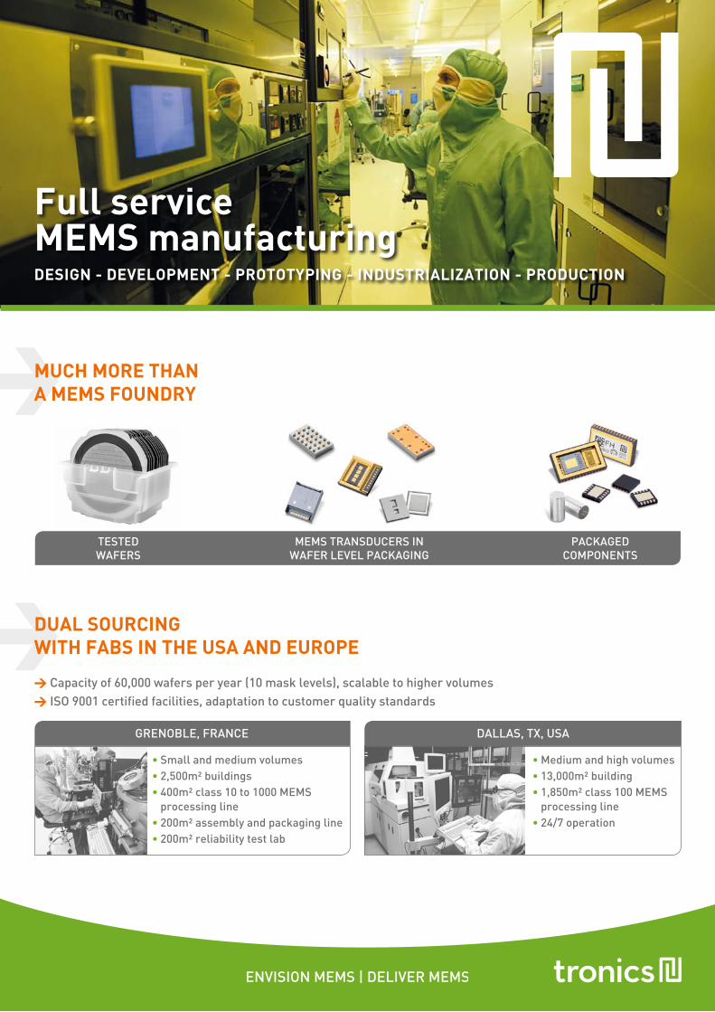
MUCH MORE THAN A MEMS FOUNDRY
• Small and medium volumes• 2,500m² buildings• 400m² class 10 to 1000 MEMS
processing line• 200m² assembly and packaging line• 200m² reliability test lab
GrEnoblE, FrancE
> capacity of 60,000 wafers per year (10 mask levels), scalable to higher volumes> ISo 9001 certified facilities, adaptation to customer quality standards
DUAL SOURCING WITH FABS IN THE USA AND EUROPE
DallaS, TX, USa
• Medium and high volumes• 13,000m² building• 1,850m² class 100 MEMS
processing line• 24/7 operation
TESTED WaFErS
MEMS TranSDUcErS InWaFEr lEvEl PackaGInG
PackaGEDcoMPonEnTS
Full service MEMS manufacturingDESIGN - DEVELOPMENT - PROTOTYPING - INDUSTRIALIZATION - PRODUCTION
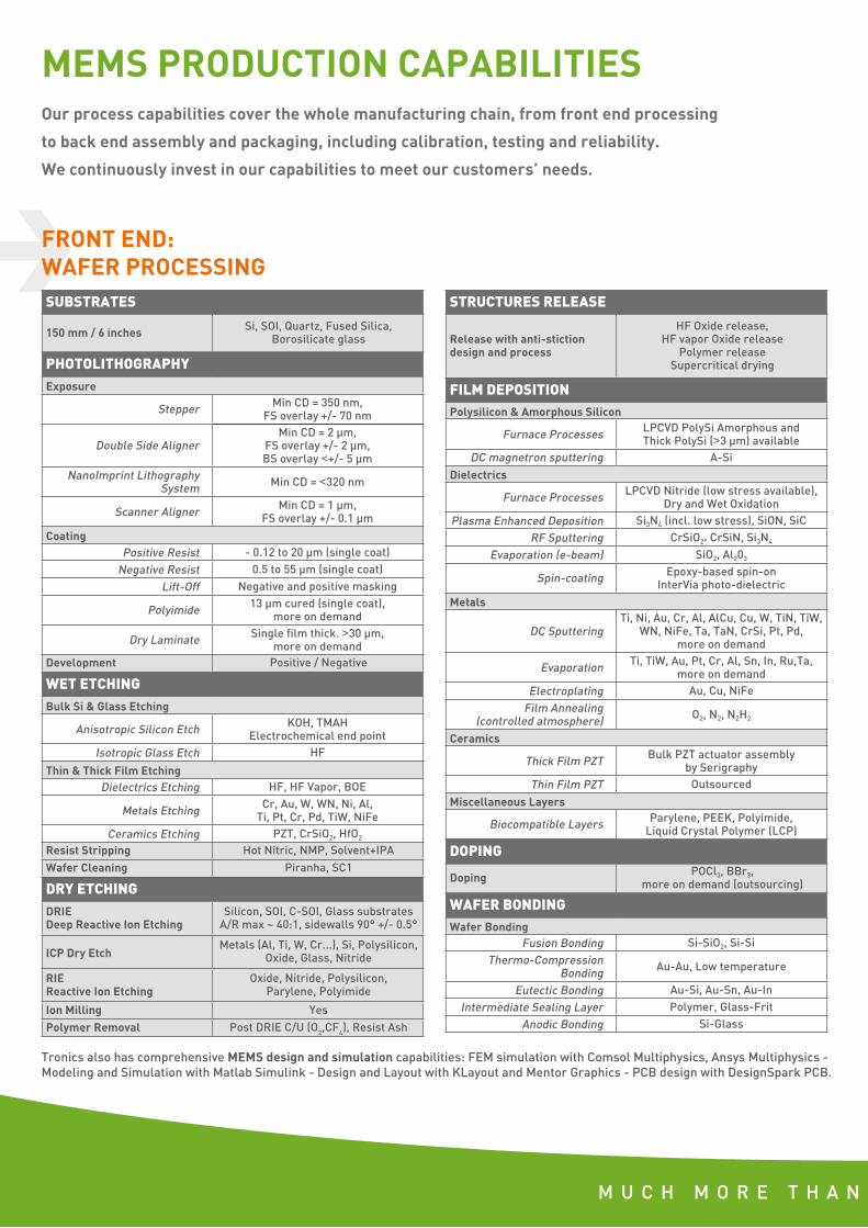
FRONT END:WAFER PROCESSING
Tronics also has comprehensive MEMS design and simulation capabilities: FEM simulation with comsol Multiphysics, ansys Multiphysics - Modeling and Simulation with Matlab Simulink - Design and layout with klayout and Mentor Graphics - Pcb design with DesignSpark Pcb.
SUBSTRATES
150 mm / 6 inches Si, SoI, Quartz, Fused Silica, borosilicate glass
PHOTOLITHOGRAPHY Exposure
Stepper Min cD = 350 nm,FS overlay +/- 70 nm
Double Side aligner Min cD = 2 µm,
FS overlay +/- 2 µm,bS overlay <+/- 5 µm
nanoImprint lithography System Min cD = <320 nm
Scanner aligner Min cD = 1 µm,FS overlay +/- 0.1 µm
CoatingPositive resist - 0.12 to 20 µm (single coat)
negative resist 0.5 to 55 µm (single coat)lift-off negative and positive masking
Polyimide 13 µm cured (single coat), more on demand
Dry laminate Single film thick. >30 µm, more on demand
Development Positive / negative
WET ETCHING Bulk Si & Glass Etching
anisotropic Silicon Etch koH, TMaHElectrochemical end point
Isotropic Glass Etch HF
Thin & Thick Film Etching Dielectrics Etching HF, HF vapor, boE
Metals Etching cr, au, W, Wn, ni, al, Ti, Pt, cr, Pd, TiW, niFe
ceramics Etching PZT, crSio2, Hfo2
Resist Stripping Hot nitric, nMP, Solvent+IPaWafer Cleaning Piranha, Sc1
DRY ETCHINGDRIEDeep Reactive Ion Etching
Silicon, SoI, c-SoI, Glass substrates a/r max ~ 40:1, sidewalls 90° +/- 0.5°
ICP Dry EtchMetals (al, Ti, W, cr...), Si, Polysilicon,
oxide, Glass, nitride
RIE Reactive Ion Etching
oxide, nitride, Polysilicon,Parylene, Polyimide
Ion Milling YesPolymer Removal Post DrIE c/U (o2,cF4), resist ash
STRUCTURES RELEASE
Release with anti-stiction design and process
HF oxide release,HF vapor oxide release
Polymer release Supercritical drying
FILM DEPOSITIONPolysilicon & Amorphous Silicon
Furnace Processes lPcvD PolySi amorphous and Thick PolySi (>3 µm) available
Dc magnetron sputtering a-Si Dielectrics
Furnace Processes lPcvD nitride (low stress available), Dry and Wet oxidation
Plasma Enhanced Deposition Si3n4 (incl. low stress), Sion, SicrF Sputtering crSio2, crSin, Si3n4
Evaporation (e-beam) Sio2, al203
Spin-coating Epoxy-based spin-on Intervia photo-dielectric
Metals
Dc SputteringTi, ni, au, cr, al, alcu, cu, W, Tin, TiW,
Wn, niFe, Ta, Tan, crSi, Pt, Pd, more on demand
Evaporation Ti, TiW, au, Pt, cr, al, Sn, In, ru,Ta, more on demand
Electroplating au, cu, niFeFilm annealing
(controlled atmosphere) o2, n2, n2H2
Ceramics
Thick Film PZT bulk PZT actuator assembly by Serigraphy
Thin Film PZT outsourced
Miscellaneous Layers
biocompatible layers Parylene, PEEk, Polyimide, liquid crystal Polymer (lcP)
DOPING
Doping Pocl3, bbr3,more on demand (outsourcing)
WAFER BONDING Wafer Bonding
Fusion bonding Si-Sio2, Si-SiThermo-compression
bonding au-au, low temperature
Eutectic bonding au-Si, au-Sn, au-InIntermediate Sealing layer Polymer, Glass-Frit
anodic bonding Si-Glass
MEMS PRODUCTION CAPABILITIESOur process capabilities cover the whole manufacturing chain, from front end processing
to back end assembly and packaging, including calibration, testing and reliability.
We continuously invest in our capabilities to meet our customers’ needs.
M U c H M o r E T H a n a M E M S F o U n D r Y
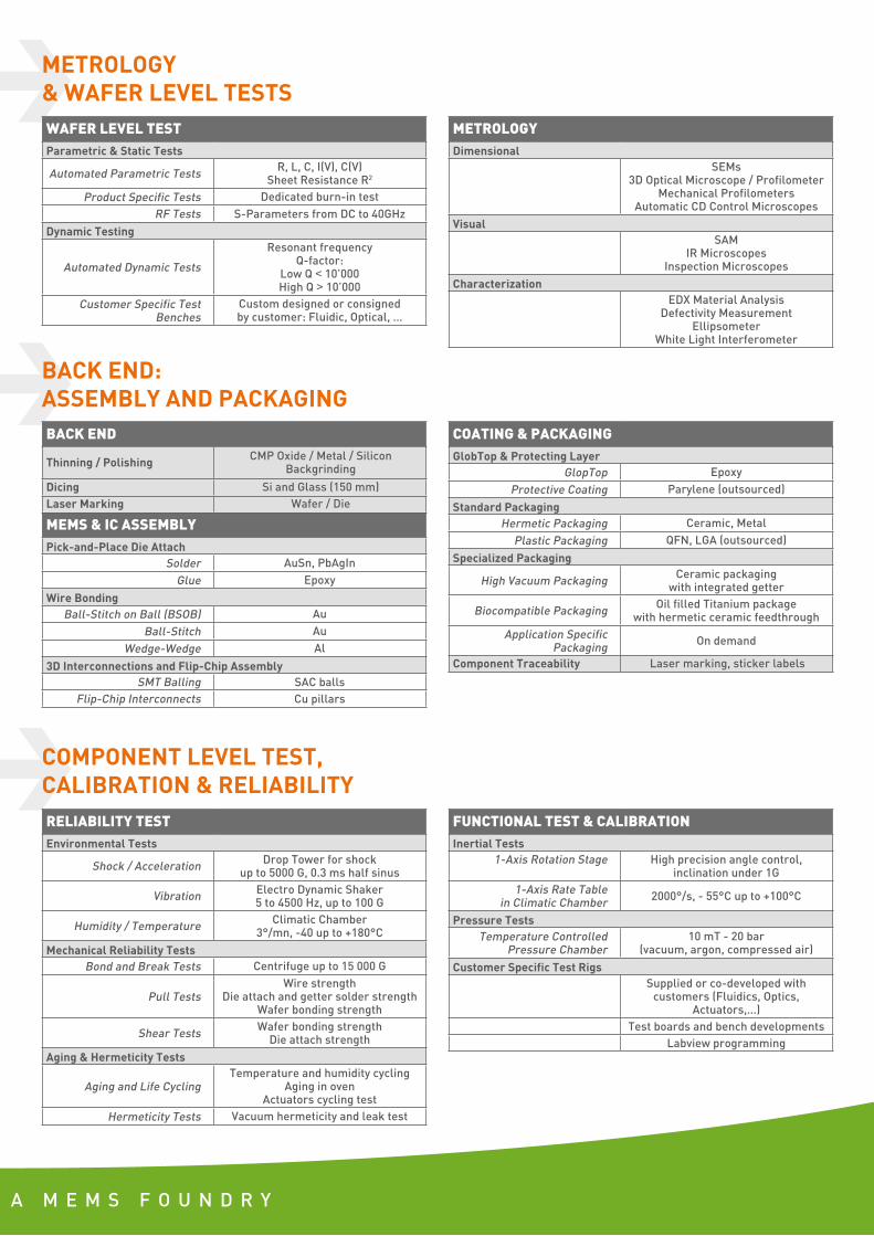
METROLOGY & WAFER LEVEL TESTS WAFER LEVEL TESTParametric & Static Tests
automated Parametric Tests r, l, c, I(v), c(v) Sheet resistance r2
Product Specific Tests Dedicated burn-in testrF Tests S-Parameters from Dc to 40GHz
Dynamic Testing
automated Dynamic Tests
resonant frequencyQ-factor:
low Q < 10’000High Q > 10’000
customer Specific Test benches
custom designed or consigned by customer: Fluidic, optical, …
METROLOGYDimensional
SEMs3D optical Microscope / Profilometer
Mechanical Profilometersautomatic cD control Microscopes
VisualSaM
Ir Microscopes Inspection Microscopes
CharacterizationEDX Material analysis
Defectivity Measurement Ellipsometer
White light Interferometer
COMPONENT LEVEL TEST, CALIBRATION & RELIABILITY RELIABILITY TESTEnvironmental Tests
Shock / acceleration Drop Tower for shock up to 5000 G, 0.3 ms half sinus
vibration Electro Dynamic Shaker5 to 4500 Hz, up to 100 G
Humidity / Temperature climatic chamber 3°/mn, -40 up to +180°c
Mechanical Reliability Testsbond and break Tests centrifuge up to 15 000 G
Pull TestsWire strength
Die attach and getter solder strengthWafer bonding strength
Shear Tests Wafer bonding strengthDie attach strength
Aging & Hermeticity Tests
aging and life cyclingTemperature and humidity cycling
aging in oven actuators cycling test
Hermeticity Tests vacuum hermeticity and leak test
FUNCTIONAL TEST & CALIBRATIONInertial Tests
1-axis rotation Stage High precision angle control,inclination under 1G
1-axis rate Table in climatic chamber 2000°/s, - 55°c up to +100°c
Pressure TestsTemperature controlled
Pressure chamber 10 mT - 20 bar
(vacuum, argon, compressed air)
Customer Specific Test RigsSupplied or co-developed with
customers (Fluidics, optics, actuators,…)
Test boards and bench developmentslabview programming
BACK END:ASSEMBLY AND PACKAGINGBACK END
Thinning / Polishing cMP oxide / Metal / Siliconbackgrinding
Dicing Si and Glass (150 mm)Laser Marking Wafer / Die
MEMS & IC ASSEMBLYPick-and-Place Die Attach
Solder auSn, PbagInGlue Epoxy
Wire Bondingball-Stitch on ball (bSob) au
ball-Stitch auWedge-Wedge al
3D Interconnections and Flip-Chip AssemblySMT balling Sac balls
Flip-chip Interconnects cu pillars
COATING & PACKAGING GlobTop & Protecting Layer
GlopTop EpoxyProtective coating Parylene (outsourced)
Standard PackagingHermetic Packaging ceramic, Metal
Plastic Packaging QFn, lGa (outsourced)
Specialized Packaging
High vacuum Packaging ceramic packaging with integrated getter
biocompatible Packaging oil filled Titanium package with hermetic ceramic feedthrough
application Specific Packaging on demand
Component Traceability laser marking, sticker labels
M U c H M o r E T H a n a M E M S F o U n D r Y
www.tronicsgroup.com
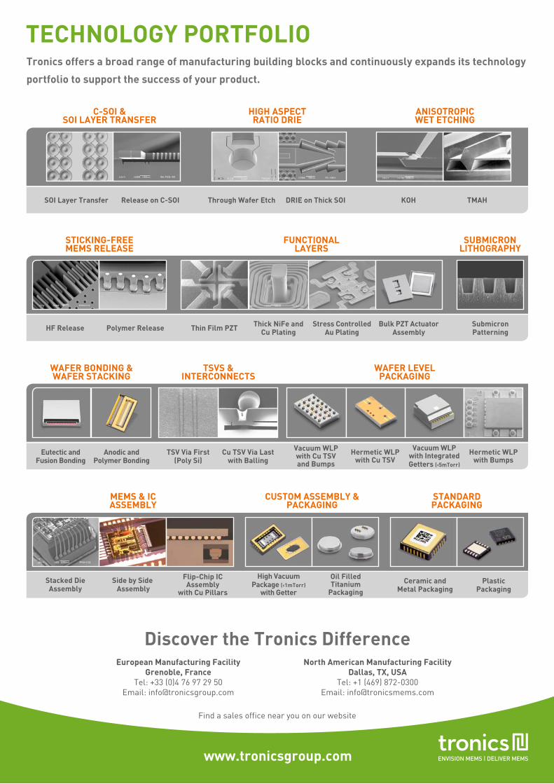
TECHNOLOGY PORTFOLIOTronics offers a broad range of manufacturing building blocks and continuously expands its technology
portfolio to support the success of your product.
Discover the Tronics DifferenceEuropean Manufacturing Facility
Grenoble, FranceTel: +33 (0)4 76 97 29 50
Email: [email protected]
North American Manufacturing FacilityDallas, TX, USA
Tel: +1 (469) 872-0300 Email: [email protected]
Eutectic and Fusion Bonding
Anodic and Polymer Bonding
SOI Layer Transfer Release on C-SOI Through Wafer Etch DRIE on Thick SOI KOH TMAH
C-SOI & SOI LAYER TRANSFER
HIGH ASPECT RATIO DRIE
ANISOTROPIC WET ETCHING
HF Release Polymer Release
FUNCTIONAL LAYERS
SUBMICRON LITHOGRAPHY
TSVS & INTERCONNECTS
CUSTOM ASSEMBLY & PACKAGING
MEMS & IC ASSEMBLY
STANDARD PACKAGING
WAFER LEVEL PACKAGING
SubmicronPatterningThin Film PZT Thick NiFe and
Cu PlatingStress Controlled
Au PlatingBulk PZT Actuator
Assembly
Vacuum WLP with Cu TSV and Bumps
Hermetic WLP with Cu TSV
Vacuum WLP with Integrated Getters (‹5mTorr)
Hermetic WLP with Bumps
Stacked Die Assembly
Side by Side Assembly
Flip-Chip IC Assembly
with Cu Pillars
High Vacuum Package (‹1mTorr)
with Getter
Oil Filled Titanium
Packaging
Ceramic and Metal Packaging
Plastic Packaging
Find a sales office near you on our website
STICKING-FREE MEMS RELEASE
WAFER BONDING & WAFER STACKING
Cu TSV Via Last with Balling
TSV Via First(Poly Si)