physical design essentials
DESCRIPTION
This is dealing with clock tree synthesis strategy of PD design.TRANSCRIPT
Y.-W. ChangUnit 8 1
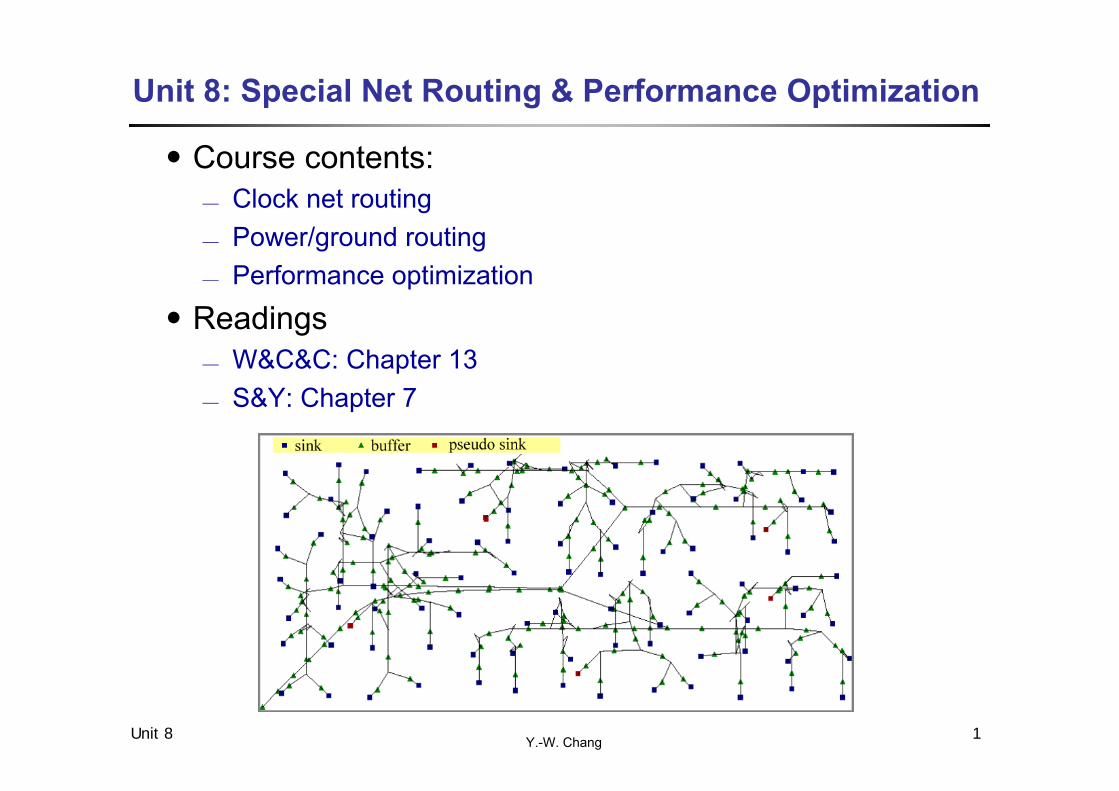
Unit 8: Special Net Routing & Performance Optimization
․Course contents: Clock net routing Power/ground routing Performance optimization
․Readings W&C&C: Chapter 13 S&Y: Chapter 7

Y.-W. ChangUnit 8 2
․ Digital systems Synchronous systems: Highly precise clock achieves
communication and timing. Asynchronous systems: Handshake protocol achieves the
timing requirements of the system.․ Clock skew: the difference in the minimum and the maximum
arrival times of the clock.
․ Clock routing: Routing clock nets such that1. clock signals arrive simultaneously2. clock delay is minimized
Other issues: total wirelength, power consumption
The Clock Routing Problem

Y.-W. ChangUnit 8 3
Clock Routing․ Given the routing plane and a set of points
P = {p1, p2, …, pn} within the plane and clock entry point p0 on the boundary of the plane, the Clock Routing Problem is to interconnect each pi P such that maxi, j P|t(0, i) - t(0, j)| and maxi P t(0, i) are both minimized.
p0 p0
p1
p5
p3
p2
p4 p6
Clock-tree synthesis (CTS): make the clock nets a tree

Y.-W. ChangUnit 8 4
Clock Routing Algorithms․ Pathlength-based Clock-Tree Synthesis (CTS)
1. H-tree: Dhar, Franklin, Wang, ICCD-84; Fisher & Kung, 1982.2. Methods of means & medians (MMM): Jackson, Srinivasan,
Kuh, DAC-90.3. Geometric matching: Cong, Kahng, Robins, DAC-91.
․ RC-delay based CTS1. Exact zero skew: Tsay, ICCAD-91.2. Deferred-merge embedding (DME) algorithm: Boese & Kahng,
ASICON-92; Chao & Hsu & Ho, DAC-92; Edahiro, NEC R&D, 1991.3. Lagrangian relaxation: Chen, Chang, Wong, DAC-96.
․ Simulation-based CTS ISPD-09 CTS contest (ASP-DAC-10, DATE-10)
․ Timing-model independent CTS Shih & Chang, DAC-10; Shih et al., ICCAD-10.
․ Mesh-based & tree-link-based clock routing

Y.-W. ChangUnit 8 5
H-Tree Based Algorithm․H-tree: Dhar, Franklin, Wang, “Reduction of clock
delays in VLSI structure,” ICCD-1984.
Similar topology: X-tree

Y.-W. ChangUnit 8 6
The MMM Algorithm․ Jackson, Sirinivasan, Kuh, “Clock routing for high-performance
ICs,” DAC-1990.․Each block pin is represented as a point in the region, S.․The region is partitioned into two subregions, SL and SR.․The center of mass is computed for each subregion.․The center of mass of the region S is connected to each of the
centers of mass of subregion SL and SR.․The subregions SL and SR are then recursively split in Y-direction.․Steps 2--5 are repeated with alternate splitting in X- and Y-
direction.․Time complexity: O(n log n).

Y.-W. ChangUnit 8 7
The Geometric Matching Algorithm․Cong, Kahng, Robins, “Matching based models for high-
performance clock routing,” IEEE TCAD, 1993.․Clock pins are represented as n nodes in the clock tree (n = 2k).․Each node is a tree itself with clock entry point being node itself.․The minimum cost matching on n points yields n/2 segments.․The clock entry point in each subtree of two nodes is the point on
the segment such that length of both sides is same.․Above steps are repeated for each segment.․Apply H-flipping to further reduce clock skew (and to handle edges
intersection).․Time complexity: O(n2 log n).
Y.-W. ChangUnit 8 8
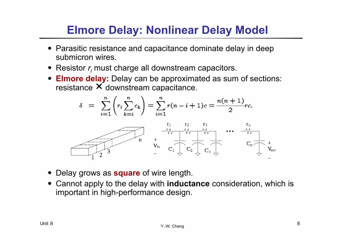
Elmore Delay: Nonlinear Delay Model․Parasitic resistance and capacitance dominate delay in deep
submicron wires.․Resistor ri must charge all downstream capacitors.․Elmore delay: Delay can be approximated as sum of sections:
resistance downstream capacitance.
․Delay grows as square of wire length.․Cannot apply to the delay with inductance consideration, which is
important in high-performance design.

Y.-W. ChangUnit 8 9
Wire Models․Lumped circuit approximations for distributed RC lines: -model
(most popular), T-model, L-model.
․-model: If no capacitive loads for C and D, A to B: AB = r1 (c1/2 + c2 + c3); B to C: BC = r2 (c2/2); B to D: BD = r3 (c3/2).

Y.-W. ChangUnit 8 10
Example Elmore Delay Computation․0.18 m technology: unit resistance = 0.075 / m; unit
capacitance = 0.118 fF/m. Assume CC = 2 fF, CD = 4 fF. BC = rBC (cBC / 2 + CC) = 0.075 150 (17.7/2 + 2) = 120 fs BD = rBD (cBD / 2 + CD) = 0.075 200 (23.6/2 + 4) = 240 fs AB = rAB (cAB/2 + CB) = 0.075 100 (11.8/2 + 17.7 + 2 + 23.6
+ 4) = 400 fs Critical path delay: AB + BD = 640 fs.

Y.-W. ChangUnit 8 11
Exact Zero Skew Algorithm․ Tsay, “Exact zero skew algorithm,” ICCAD-91.․ To ensure the delay from the tapping point to leaf nodes of subtrees T1
and T2 being equal, it requires thatr1 (c1/2 + C1) + t1 = r2 (c2/2 + C2) + t2.
․ Solving the above equation, we have
where and are the per unit values of resistance and capacitance, l the length of the interconnecting wire, r1 = xl, c1 = xl, r2 = (1 - x)l, c2 = (1 - x)l.
Y.-W. ChangUnit 8 12
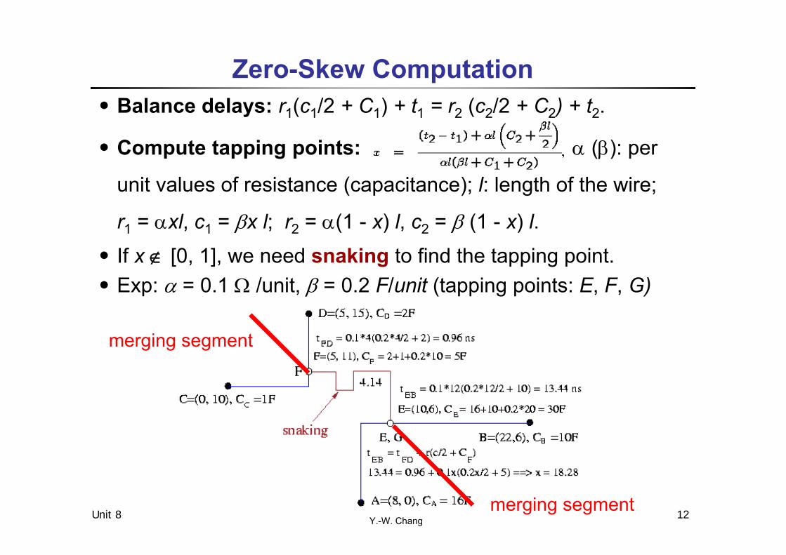
Zero-Skew Computation․Balance delays: r1(c1/2 + C1) + t1 = r2 (c2/2 + C2) + t2.
․Compute tapping points: (): per
unit values of resistance (capacitance); l: length of the wire;
r1 = xl, c1 = x l; r2 = (1 - x) l, c2 = (1 - x) l.․If x [0, 1], we need snaking to find the tapping point.․Exp: = 0.1 /unit, = 0.2 F/unit (tapping points: E, F, G)
merging segment
merging segment
Y.-W. ChangUnit 8 13
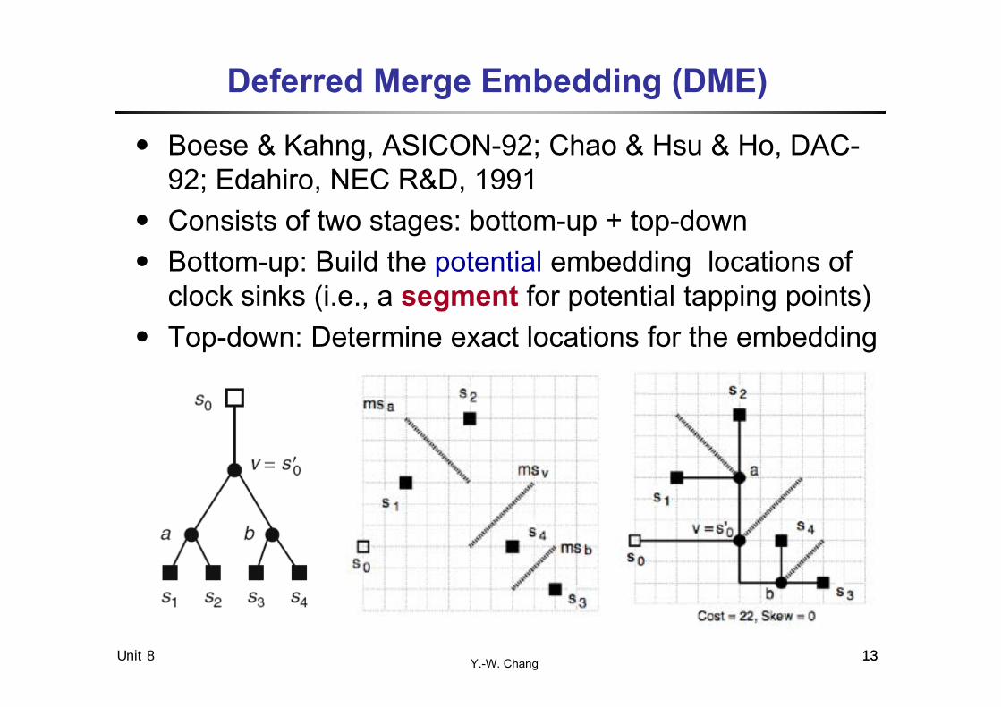
Deferred Merge Embedding (DME)
․ Boese & Kahng, ASICON-92; Chao & Hsu & Ho, DAC-92; Edahiro, NEC R&D, 1991
․ Consists of two stages: bottom-up + top-down․ Bottom-up: Build the potential embedding locations of
clock sinks (i.e., a segment for potential tapping points)․ Top-down: Determine exact locations for the embedding
13

Y.-W. ChangUnit 8 14
Delay Computation for Buffered Wires․Wire: = 0.068 /m, = 0.118 fF/ m2; buffer: ' = 180 / unit
size, ' = 23.4 fF/unit size; driver resistance Rd = 180 ; unit-sized wire, buffer.

Y.-W. ChangUnit 8 15
Buffering and Wire Sizing for Skew Minimization․Discrete wire/buffer sizes: dynamic programming
Chung & Cheng, “Skew sensitivity minimization of buffered clock tree,” ICCAD-94.
․Continuous wire/buffer sizes: mathematical programming (e.g., Lagrangian relaxation) Chen, Chang, Wong, “Fast performance-driven optimization for
buffered clock trees based on Lagrangian relaxation,” DAC-96. Considers clock skew, area, delay, power, clock-skew
sensitivity simultaneously.

Y.-W. ChangUnit 8 16
Clock Meshes․More alternative paths to clock sinks
Good for high-performance circuits with stringent skew and variation constraints
․Drive mesh from the boundary or from grid points․H-tree is a good candidate to drive mesh
Alpha 21264 processor [Bailey et al. 1998] IBM Power4 processor [Anderson et al. 2001]

Y.-W. ChangUnit 8 172.89V 2.95V
1.46V 2.23V1.8V
SM1
SM2
HM1
HM2 HM3
3V
Power consumption and rail parasitics cause actual supply voltage to be lower than ideal Metal width tends to decrease with length increasing in
nanometer design
Effects of IR drop Reducing voltage supply reduces circuit speed (5% IR drop =>
15% delay increase) Reduced noise margin may cause functional failures
SM2
SM1
HM2
HM1HM3
SM2
HM1
HM2 HM3
SM1
SM2
violation
Power Integrity: IR (Voltage) Drop

Y.-W. ChangUnit 8 18
Power/Ground (P/G) Routing․ Are usually laid out entirely on metal layers for
smaller parasitics.․ Two steps:
1. Construction of interconnection topology: non-crossing power, ground trees.
2. Determination of wire widths: prevent metal migration, keep voltage (IR) drop small, widen wires for more power-consuming modules and higher density current (1 mA / m2
at 25 oC for 0.18 m technology). (So area metric?)

Y.-W. ChangUnit 8 19
Power/Ground Network Optimization
․Use the minimum amount of chip area for wiring P/G networks while avoiding potential reliability failures due to electromigration and excessive IR drops.
․Tan and Shi, “Fast power/ground network optimization based on equivalent circuit modeling”, DAC-2001. Build the equivalent models for series resistors and apply a
sequence of the linear programming (SLP) method to solve the problem.
Size wire segments assuming the topologies of P/G networks to be fixed.
․Wu and Chang, “Efficient power/ground network analysis for power integrity driven design methodology,” DAC-2004.
․Liu and Chang, “Floorplan and power/ground co-synthesis for fast design convergence,” ISPD-06 (TCAD-07).

Y.-W. ChangUnit 8 20
Problem Formulation․Let G = {N, B} be a P/G network with n nodes N = {1, …, n} and b
branches B = {1, …, b}; branch i connects two nodes: i1 and i2 with current flowing from i1 to i2.
․Let li and wi be the length and width of branch i, respectively. Let ρbe the sheet resistivity. Then the resistance ri of branch iis .
․Total P/G routing area is as follows:
․P/G network optimization is to minimize f(V, I) subject to the constraints listed in the next slide.
․Relax the nonlinear objective function and then translate the constrained nonlinear programming problem into a SLP problem.
i
i
i
iii
wl
IVr v
21
i1 i2wi
li

Y.-W. ChangUnit 8 21
Constraints․The voltage IR drop constraints.
for power networks. for ground networks.
․The minimum width constraints:
․The electro-migration constraints: Ii/wi ≤ σ =>
σ is a constant for a particular routing layer with a fixed thickness.
․Equal width constraints: or
․Kirchoff ’s current law (KCL):
For each node j = {1, …, n}, B(j) is the set of indices of
branches connecting to node j.
,
min
max
,h
l
i
i
V VV V
min,21
iii
iii w
VVIlw
iii lVV 21
ji ww jj
jj
ii
ii
Ilvv
Ilvv 2121
0)(
jBi
iI
Y.-W. ChangUnit 8 22
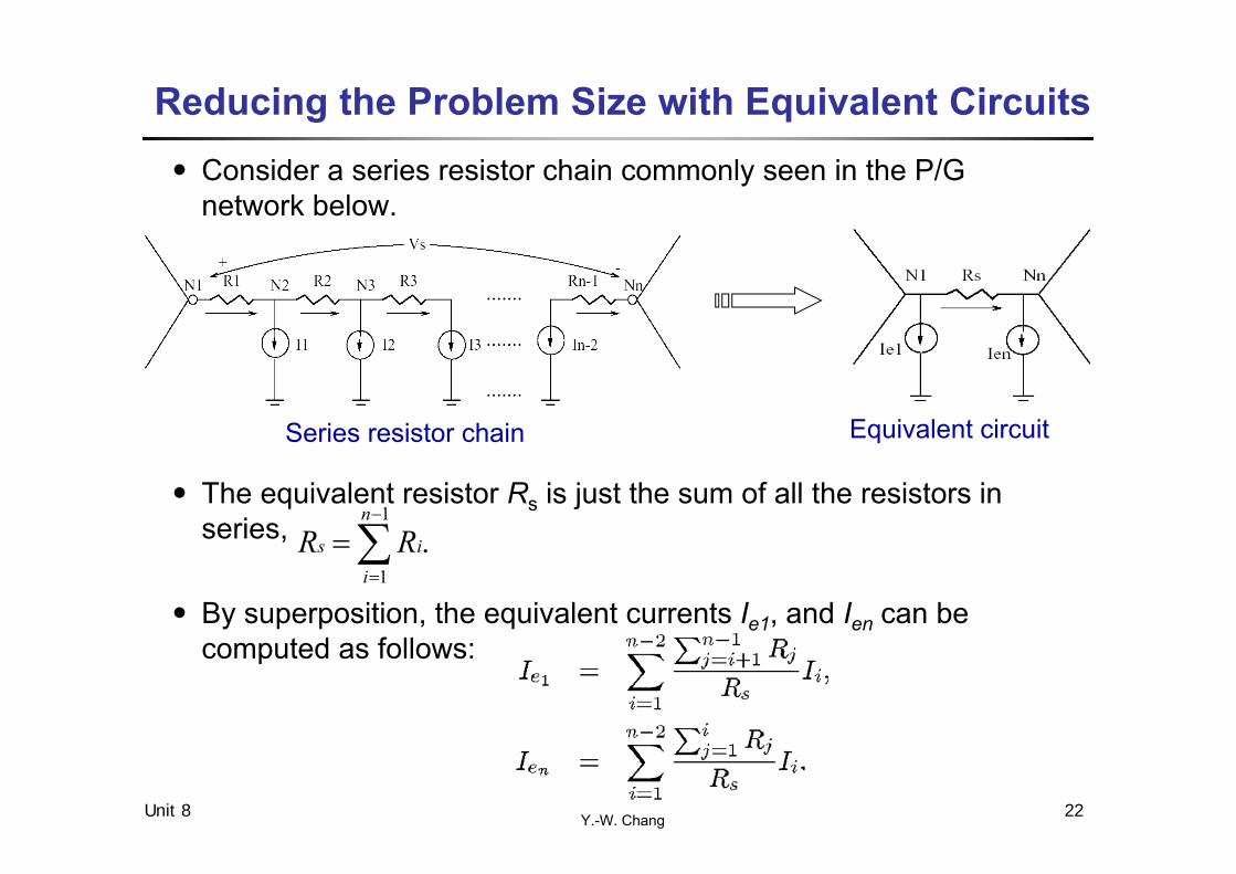
Reducing the Problem Size with Equivalent Circuits․Consider a series resistor chain commonly seen in the P/G
network below.
․The equivalent resistor Rs is just the sum of all the resistors in series,
․By superposition, the equivalent currents Ie1, and Ien can be computed as follows:
.1
1
n
iis RR
Series resistor chain Equivalent circuit

Y.-W. ChangUnit 8 23
Equivalent Circuit (cont’d)
․The voltages at the intermediate nodes are calculated based on superposition as follows:
iee
eiss
iii
III
IRVRRVV
ii
i
1
1
Series resistor chain Equivalent circuit

Y.-W. ChangUnit 8 24
Equivalent Circuit Example

Y.-W. ChangUnit 8 25
Floorplanning
P&R
RC Extraction
Simulation
SI Analysis
iterative loopOK
yes
no
․IR-drop aware design methodology for faster design convergence
Design Methodology Evolution
IR-drop Analysis
Floorplanning
P&R
RC Extraction
Simulation
iterative loopOK
SI Analysis
yes
no
IR-drop Analysis
P&R
RC Extraction
Simulation
SI Analysis
Floorplanning
Traditional flow DAC-04 flow (Wu & Chang)
ISPD-06 (TCAD-07) flow(Liu & Chang)

Y.-W. ChangUnit 8 26
Ideal Scaling of MOS Transistors․Feature size scales down by S times:

Y.-W. ChangUnit 8 27
Ideal Scaling of Interconnections․Feature size scales down by S times:

Y.-W. ChangUnit 8 28
Techniques for Higher Performance․In very deep submicron technology, interconnect delay
dominates circuit performance.․Techniques for higher performance
SOI: lower gate delay. Copper interconnect: lower resistance. Dielectric with lower permittivity: lower capacitance. Buffering: Insert (and size) buffers to “break” a long
interconnection into shorter ones. Wire sizing: Widen wires to reduce resistance (careful for
capacitance increase). Shielding: Add/order wires to reduce capacitive and inductive
coupling. Spacing: Widen wire spacing to reduce coupling. Others: padding, track permutation, net ordering, etc.

Y.-W. ChangUnit 8 29
Interconnect Dominates Circuit Performance!!
10
20
30
40
50
60
70
650 500 350 250 180 150 100 70 (nm)
Worst-caseinterconnectdelay dueto crosstalk
Interconnectdelay
Technology Node
Del
ay (p
s)
Gate delay
CWCSIn ≦ 0.18μm wire-to-wire capacitance dominates (CW>>CS)

Y.-W. ChangUnit 8 30
Optimal Buffer Sizing w/o Considering Interconnects
․Delay through each stage is tmin, where tmin is the average delay through any inverter driving an identically sized inverter.
․n = CL/Cg n = ln (CL/Cg)/ln , where CL is the capacitive load and Cg the capacitance of the minimum size inverter.
․Total delay .
․Optimal stage ratio:
․Optimal delay:
․Buffer sizes are exponentially tapered ( = e).

Y.-W. ChangUnit 8 31
Wire Sizing․Wire length is determined by layout architecture, but we can
choose wire width to minimize delay.․Wire width can vary with distance from driver to adjust the
resistance which drives downstream capacitance.․Wire with minimum delay has an exponential taper.․Can approximate optimal tapering with segments of a few
widths.․Recent research claims that buffering is more effective than
wire sizing for optimizing delay, and two wire widths are sufficient for area/delay trade-off.

Y.-W. ChangUnit 8 32
․ Suppose a wire of length L is partitioned into n equal-length wire segments, each of length x = L/n; unit resistance and capacitance: , .
․ The respective resistance and capacitance of i-th wire segment can be approximated by x / f(xi) and x f(xi), where f(xi) is the width at position xi.
․ Elmore delay:
․ As n , Dn D:
․ Optimal wire sizing function f(x) = ae-bx, where
Optimal Wire-Sizing Function
x

Y.-W. ChangUnit 8 33
Simultaneous Wire & Buffer Sizing․ Input: Wire length L, driver resistance Rd, load capacitance CL,
unit wire area capacitance c0, unit wire fringing capacitance cf, unit-sized wire resistance r0, unit-size capacitance of a buffer cb, unit-size buffer resistance rb, intrinsic buffer delay Tin, and the number of buffers N.
․Objective: Determine the stage ratio for buffer sizes and the stage ratio for wire widths such that the wire delay is minimized.

Y.-W. ChangUnit 8 34
Wire/Buffer Size Ratios for Delay Optimization․Chang, Chang, Jiang, ISQED-2002.
․ In practice, the delay of a wire DN(, ) is a convex function of the stage ratio for practical buffer sizes and the stage ratio for practical wire widths.
․Can apply efficient search techniques (e.g., binary search) to find the optimum ratios.

Y.-W. ChangUnit 8 35
Performance Optimization: A Sizing Problem
• Minimize the maximum delay Dmax by changing w1,…,wn
niUwLmiDDtosubject
DMinimize
i
i
..1 , ..1 ,)(
max
max
w
w1
w2
w9
w10
w11 w6w8w3
w5
w4w7
D1<Dmax
D2<Dmax
a
b

Y.-W. ChangUnit 8 36
Popular Sizing Works․ Algorithmic approaches: faster, non-optimal for general problems
TILOS (Fishburn, Dunlop, ICCAD-85) Weighted Delay Optimization (Cong et al., ICCAD-95)
․ Traditional mathematical programming: often slower, optimal Geometric Programming (TILOS) Augmented Lagrangian (Marple et al., 86) Sequential Linear Programming (Sapatnekar et al.) Interior Point Method (Sapatnekar et al., TCAD-93) Sequential Quadratic Programming (Menezes et al., DAC-95) Augmented Lagrangian + Adjoin Sensitivity (Visweswariah, et
al., ICCAD-96, ICCAD-97)․ Lagrangian relaxation based mathematical
programming: (Chen, Chang, Wong, DAC-96; Jiang, Chang, Jou, DAC-99 [TCAD, Sept. 2000]; and many more)
Fast and optimal

Y.-W. ChangUnit 8 37
TILOS: Heuristic Approach
• Finds sensitivities associated with each gate• Up-sizes the gate with the maximum sensitivity• Minimizes the objective function
Minimize Dmax
w1
w2
w9
w10
w11 w6w8w3
w5
w4w7
D1<Dmax
D2<Dmax
a
b

Y.-W. ChangUnit 8 38
Weighted Delay Optimization
DriverLoads
• Cong, et. al., ICCAD-95• Sizes one wire at a time in the DFS order• Minimize the weighted delay • Best weights?
w3
w5w4
w1 w2 1D1
2D2
Minimize 1D1 2D2

Y.-W. ChangUnit 8 39
From Mathematical Prog. to Lagrangian Relaxation
min cxst Axb
xX
Mathematicalformulation
Posynomialforms
Positive coefficient polynomials
min L()=cx + (Ax-b)st xX
Lagrange multipliers

Y.-W. ChangUnit 8 40
Mathematical Programming
• Formulation:
• Lagrangian:
• Optimality (Necessary) Condition (Kuhn-Tucker theorem):
( ) ( ) ( ), 01
mL f x g x wherei i ii
Condition)ty (Feasibili 0 ,0)(
Condition)tary (Complemen 0)(
01
)()(0)(
ixig
xigi
m
ixigixf
xL
i
λ
mixgtosubjectxfMinimize
i ..1 ,0)( )(

Y.-W. ChangUnit 8 41
Lagrangian Relaxation
1 ( ) ( )
( ) 0, 1..
n
i ii
i
Minimize f x g x
subject to g x i n m
( ) ( ) 0, 1..
( ) 0, 1..i
i
Minimize f xsubject to g x i n
g x i n m
LRS
․ LRS (Lagrangian Relaxation Subproblem)․ There exist Lagrangian multipliersλthat lead LRS to
the optimal solution for convex programming When f(x), gi(x)’s are all positive polynomials
(posynomials)․ The optimal solution for any LRS is a lower bound
of the original problem

Y.-W. ChangUnit 8 42
Lagrangian Relaxation
niUwLmiDD
D
i
i
..1 , ..1 ,)( subject to
Minimize
max
max
w
niUwL
DDD
i
i
m
ii
..1 , subject to
))(( Minimize max1
max
w
niUwL
D
i
i
m
ii
..1 , osubject t
)( Minimize1
w
m
iiλ ,
DL
1max
1have we0By
Lagrangian Relaxation
λ
L λ

Y.-W. ChangUnit 8 43
Lagrangian Relaxation
SLP
SQP
Augmented Lagrangian
TILOS
Weighted Delay
MathematicalProgramming
Algorithmicapproaches
LagrangianRelaxation

Y.-W. ChangUnit 8 44
Lagrangian Relaxation Framework
Update Multipliers
Weighted DelayOptimization
Converge?No
Yes
done

Y.-W. ChangUnit 8 45
Lagrangian Relaxation Framework
D1
D2
Dmax
D1 D2
Dmax
D1 D2
1 21 2
More Critical -> More Resource -> Larger Weight

Y.-W. ChangUnit 8 46
Weighted Minimization
w2 w3
w1D1
D2
a
b
Minimize 1D1 2D2
․ Traverse the circuit in the topological order․ Resize each component to minimize Lagrangian during
visit

Y.-W. ChangUnit 8 47
Multiplier Adjustment: A Subgradient Approach
solution feasiblenearest the toProject :2 Step
,0lim
),( :1 Step
1kk
max
λ
kk
ikoldi
newi
where
DD
․ Subgradient: An extension definition of gradient for non-smooth functions.
․ Experience: Simple heuristic implementation can achieve a very good convergence rate.

Y.-W. ChangUnit 8 48
Convergence Sequence
Lagrangian = Lower BoundWeighted Delay <= Maximum Delay
Any Feasible Maximum Delay =Upper Bound
Optimal Solution
# Iterations
Max Delay niUwLtosubject
DMinimize
i
i
m
ii
..1 ,
)( 1
w

Y.-W. ChangUnit 8 49
Path Delay Formulation
d1 d2
d3
D1
D2
23
231
121
121
DdADddADddADddA
c
b
b
a
AaAb
Ac
• Exponential growth• More accurate • Can exclude false paths

Y.-W. ChangUnit 8 50
Stage Delay Formulation
d1 d2
d3
D1
D2
23
23
12
1
1
DdADdADdAAdAAdA
c
e
e
eb
ea
AaAb
Ac
Ae
• Polynomial size• Less accurate• Contains false paths

Y.-W. ChangUnit 8 51
Both Multipliers Satisfy KCL (Flow Conservation)
iioutputkik
iinputjji
)()(
1
2
34
5
43
32
31
53
43 5331 32
iioutputkik
iinputjji
)()(
1
2
4
5
3,in 3,out
41
42
51
52
3
Path BasedStage Based

Y.-W. ChangUnit 8 52
Appendix A:
Shih and Chang“Fast timing-model independent clock-tree synthesis”
DAC-10, TCAD-12

Y.-W. ChangUnit 8 53
․Skew-minimized buffered clock-tree synthesis plays an important role in VLSI designs for synchronous circuits
․Due to the insufficient accuracy of timing models, embedding simulation into synthesis becomes inevitable
․Runtime becomes prohibitively huge as design complexity grows
time-consuminginsufficient accuracy
Introduction
53
timing
timing?
merging vdd
vss
solution?
?
?

Y.-W. ChangUnit 8 54
․Skew is minimized by structural optimization․Buffering and wiring of all paths are almost the same
Is timing-model independent Do not need simulation information
Symmetrical Structure
54
0ps skew (Elmore delay)0.123ps skew (simulation)
n1 (12,26)n2(3,29)
n4 (1,57)
n5 (5,1)
n6 (33,29)
n7 (33, 9)
n3 (33,19)
snaking
0ps skew (Elmore delay)0ps skew (simulation)
n'3 (21,23)
n1n2
n4
n5
n6
n7

Y.-W. ChangUnit 8 55
Problem Formulation
․Problem: Buffered Clock-Tree Synthesis (BCTS)
․Instance Given a set of clock sinks, a slew-rate constraint,
and a library of buffers
․Question Construct a buffered clock tree to minimize its skew,
subject to no slew-rate violation
55
Y.-W. ChangUnit 8 56
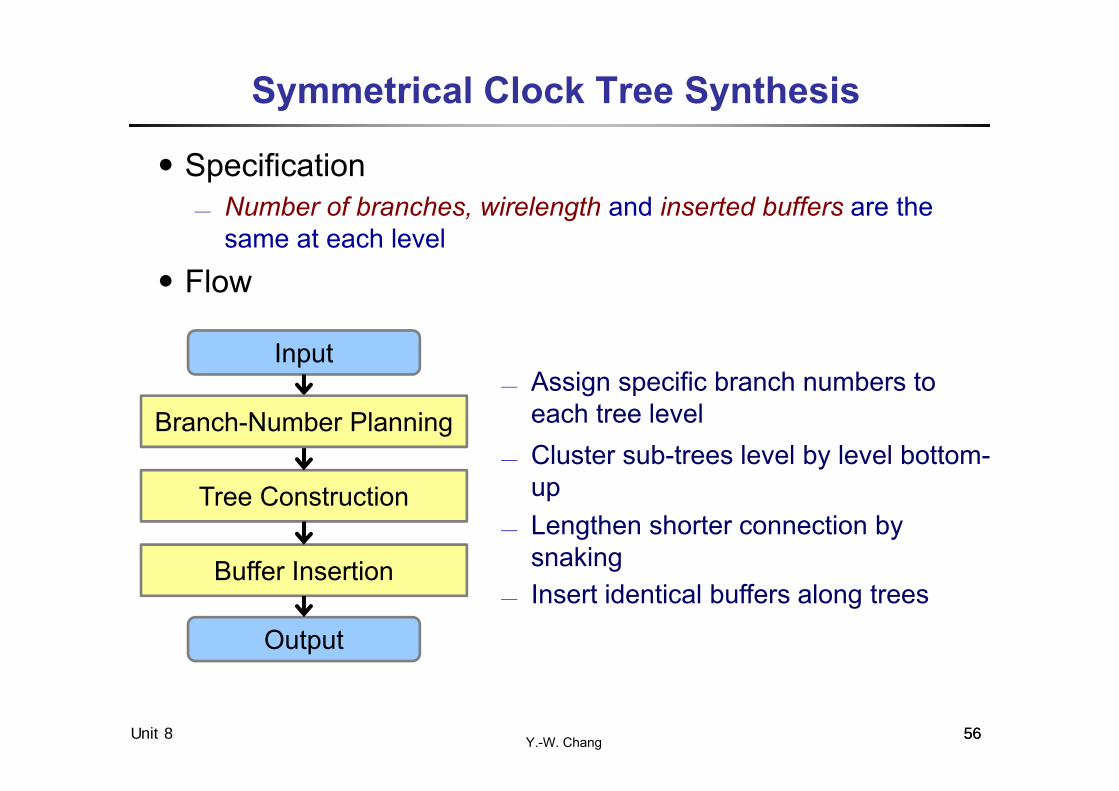
Symmetrical Clock Tree Synthesis
․Specification Number of branches, wirelength and inserted buffers are the
same at each level․Flow
56
Tree Construction
Buffer Insertion
Input
Output
Branch-Number Planning Assign specific branch numbers to
each tree level Cluster sub-trees level by level bottom-
up Lengthen shorter connection by
snaking Insert identical buffers along trees

Y.-W. ChangUnit 8 57
Branch-Number Planning
․Observation Total branch number of some level equals the number of
preceding level times its branch number The multiplication sequence forms a factorization
․Planning Branch-Number Plan (BNP) is arranged in non-increasing order
57
prime
level-1 branch number
total number of primes

Y.-W. ChangUnit 8 58
Branch-Number Planning
․Factorization may result in a big branch number, implying a large fan-out size that could not be driven
․Pseudo sinks are added to increase the total sink number until all branch numbers are feasible
58
……………
3
33222
branches
sinks
BNP = B(216) = < 3, 3, 3, 2, 2, 2 >
pseudo sinks
branches
…………
…
3
33222…
BNP = B(212+4) = < 3, 3, 3, 2, 2, 2 >BNP = B(212) = < 53, 2, 2 >BNP = B(212+1) = < 71, 3 >BNP = B(212+2) = < 107, 2 >BNP = B(212+3) = < 43, 5 >

Y.-W. ChangUnit 8 59
Tree Construction
․Achieve identical wirelength in this stage Cluster sub-trees level by level bottom-up Lengthen shorter connection by snaking
․Flow
59
Partitioning
Embedding-Region Construction
Node Embedding
Root?Y
N
Divide sub-trees into desired clusters Apply a common connection length to
each cluster, and locate potential embedding positions to which snaked wires can reach
Repeat the two stages till the embedding region of the root is built
Find exact physical locations for nodes and route wires top-down

Y.-W. ChangUnit 8 60
Tilted Rectangular Region (TRR)․Represents potential embedding positions (embedding
region)․Is a 45- or 135-degree rectangular region
core: a 45- or 135-degree line segment radius: the Manhattan distances from the core to the region
boundaries
60
radius
core
extended radius
extended TRR
Manhattandistance
TRRi
TRRj
Configuration Operation Definition

Y.-W. ChangUnit 8 61
․The objective is to minimize cluster diameter Cluster diameter: the maximum distance among sub-trees
within the same cluster Maximum cluster diameter is the upper bound of the common
connection length․Sub-trees are divided recursively along the BNP in a
top-down manner․Non-binary tree can also be handled by this technique
Partitioning
61
maximum cluster diameter

Y.-W. ChangUnit 8 62
Dividing: Cake Cutting․Borrow the idea of cake cutting, i.e., slicing a cake into
pieces from the center of the cake․Sort the polar angles of sub-trees relative to the
geometric center of the cluster․Apply dynamic programming to find the minimum cluster
diameter by restricting the dividing on this sorted order
62
center pointcluster diameter
Input Sinks Polar-Angles Sorting Divided Result

Y.-W. ChangUnit 8 63
Recursive Dividing․For i-th level partitioning along the given BNP
<b1, b2, …, bq>, dividing is performed recursively until b1 x b2 x … x bi-1 clusters are derived
․Desired cluster diameter could be obtained since global sub-tree distribution is considered throughout the whole process
63
Recursive Dividing Final Divided Result Corresponding Clusters

Y.-W. ChangUnit 8 64
Embedding-Region Construction․Assign the common connection length (CCL) as the half
length of the maximum cluster diameter․Extend the TRRs of children nodes and make
intersection to construct the embedding region of their parents
64
CCL CCL
embedding region
Given Divided Result Region Extension/Intersection Resulting Regions
Y.-W. ChangUnit 8 65
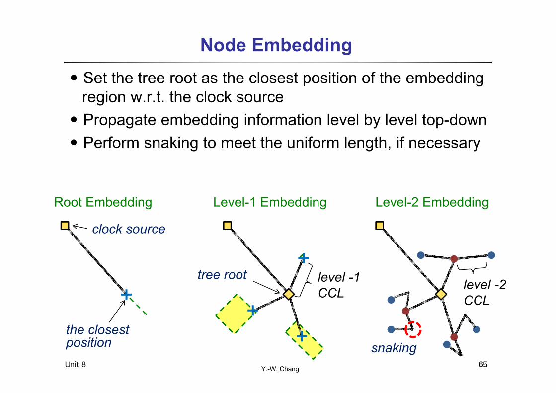
Node Embedding․Set the tree root as the closest position of the embedding
region w.r.t. the clock source․Propagate embedding information level by level top-down ․Perform snaking to meet the uniform length, if necessary
65
clock source
the closest position
level -2CCL
snaking
level -1CCL
tree root
Root Embedding Level-1 Embedding Level-2 Embedding
Y.-W. ChangUnit 8 66
Pseudo-Sink Handling
․For partitioning Relax the sizes of clusters in a partition which can
differ by at most one for the first recursion․For embedding-region construction
Construct no embedding regions for pseudo sinks to reserve the flexibility of snaking
․For node embedding Let the embedding regions of pseudo sinks cover
entire chip․Dangling wires can be identified and attached to proper
sub-trees successfully
66

Y.-W. ChangUnit 8 67
Buffer Insertion․Align buffer distribution on the symmetrical tree
topology․Insert identical buffers level by level top-down
67
First-Time Insertion Second-Time Insertion Third-Time Insertion

Y.-W. ChangUnit 8 68
Experimental Results on IBM Benchmarks
․Our approach can obtain much smaller skews in much shorter runtime than the state of the art, with marginal overheads of snaking for symmetry
68
Circuit # sinks
Shih et al. [ASPDAC’10] w/o simulation
Shih et al. [ASPDAC’10] w/ simulation
Ours
skew usage runtime skew usage runtime skew usage runtime(ps) (fF) (s) (ps) (fF) (s) (ps) (fF) (s)
r1 267 14.005 14001 2 5.012 15229 5126 1.510 13829 0.070 r2 598 16.012 28011 11 6.421 29234 7374 1.770 31056 0.280 r3 862 16.532 39123 26 5.611 41431 12739 2.310 44188 1.050 r4 1903 17.792 89312 165 5.418 91015 17871 2.540 98450 3.350 r5 3101 21.557 149875 498 7.028 156854 26045 3.010 171228 5.560
avg. comparison 7.93 0.92 46.29 2.77 0.96 24343.13 1.00 1.00 1.00
More than 80000X faster than the ISPD-09 contest winners (simulation-based methods)

Y.-W. ChangUnit 8 69
Resulting Clock Tree: ispd09f22
69

Y.-W. ChangUnit 8 70
Appendix B:Liu and Chang
“Floorplan and power/ground network co-synthesis for fast design convergence”
ISPD-06 (TCAD-07)
A B
B
A

Y.-W. ChangUnit 8 71
Floorplan & P/G Network Co-Synthesis
․Liu and Chang, “Floorplan and power/ground network co-synthesis for fast design convergence,” ISPD-06 (TCAD-07).
․Apply the B*-tree floorplan representation and simulated annealing (SA)
․Analyze the P/G network (typical flow) Circuit modeling Global P/G network construction P/G network modeling/reduction P/G network evaluation (IR-drop computation)
․Reduce floorplan solution space

Y.-W. ChangUnit 8 72
Implementation of the Design Flow
Data preparation․Power profile
Power consumption data of the modules generated by PrimePower
․Hierarchical circuit partition Organize the design into hard
modules and soft modules according to the hierarchy
Post-layout verification․AstroRail
Static cell-level P/G analysis

Y.-W. ChangUnit 8 73
Simulated Annealing Process
․Non-zero probability for up-hill climbing:
․Perturbations (neighboring solutions) Op1: Rotate a block Op2: Move a node/block to
another place Op3: Swap two nodes/blocks Op4: Resize a soft block
․The cost function Ψ is basedon the floorplan cost and P/G network cost
․T is decreased every n cycles, where n is proportional to the number of blocks
Tep ,1min
Update TConstruct P/G network
Evaluate cost Ψ
NCool/Good
enough?
Y
Pack B*-tree
Initialize B*-tree and temperature T
Better ?
Keep solutionRecover last
solution
Accept?
Update P/G pitch Dpitch
NYY
N
Perturb B*-tree

Y.-W. ChangUnit 8 74
․Cost function:
․W: Wirelength․A : Area․Φ : P/G network cost (penalty of power integrity violation)․Dpitch: pitch of P/G network
Increasing power mesh density (reducing Dpitch) reduces Φ Update Dpitch by multiplying : Average P/G network cost at a temperature : , a factor for adjusting the density of P/G networks
Smaller for higher P/G density and larger one for lower P/G density
Cost Function
,2pitchDAAW
avg /ˆ
avg
1ˆ0
Wirelength Area P/G cost P/G Density

Y.-W. ChangUnit 8 75
-1
0
1
2
3
4
0.000010.00010.0010.010.110.01
0.1
1
10
100
1000
․At the beginning of SA, Dpitch = 2 and ․During SA process,
converges to 1 while temperature cools down
Pitch Updating: An Example
avg /ˆ
02.0ˆ
Temperature
Dpitch Dpitchavg /ˆ
avg /ˆ
SA process
pitchavgpitch DD /

Y.-W. ChangUnit 8 76
P/G Network Cost
Φ: P/G network cost
․Bem: set of branches violating electromigration constraints․B : total branches of the P/G mesh․vpvi: amount of the violation at the pin pvi
․P : set of all P/G pins․Pv : set of violating P/G pins․Vlim,pi : IR-drop constraint of the P/G pin pi
lim,
(1 ) ,vivi vpp Pem
piPi P
vBB V
EM cost IR-drop cost
10

Y.-W. ChangUnit 8 77
P/G Network Construction
․For each floorplan, we construct a uniform global P/G network according to Dpitch
1 2 3
1
․The number of trunks is defined by round[width/Dpitch]+1 & round[height/Dpitch]+1
Floorplan
Width
Height
2X4 uniform P/G network is constructed
Calculate the P/G network dimension
3+1 =4
1+1 =2

Y.-W. ChangUnit 8 78
P/G Network ModelingApply static analysis for fast P/G network evaluation․Use resistive P/G Model ․Model P/G pins by current sources
Current value: maximum current drawn from P/G pins․Reduce circuit size
Connect current sources to nearest global trunk nodesPower pad Module
Power pin
Power trunk
Power strap
Global trunk node

Y.-W. ChangUnit 8 79
P/G Network ModelingApply static analysis for fast P/G network evaluation․Use resistive P/G Model ․Model P/G pins by current sources
Current value: maximum current drawn from P/G pins․Reduce circuit size
Connect current sources to nearest global trunk nodesPower pad Module
Power pin
Power trunk
Power strap
Reduced circuit

Y.-W. ChangUnit 8 80
Macro Current Modeling․Divide the floorplan into regions․For hard macros
Connect P/G pins to the nearest global trunk nodes․For soft macros (worst-case scenario)
Collect the largest current drawn by standard cells in the overlapping area of the region and the soft macro
d/2 d/2d
Hard module
Soft module
The border line of the region is defined by the center of the global
trunk nodes

Y.-W. ChangUnit 8 81
Macro Current Modeling․Divide the floorplan into regions․For hard macros
Connect P/G pins to the nearest global trunk nodes․For soft macros (worst-case scenario)
Collect the largest current drawn by standard cells in the overlapping area of the region and the soft macro
d/2 d/2d
Overlapping Area
Assign current to the global trunk nodes of the regions

Y.-W. ChangUnit 8 82
Soft Macro Modeling
Standard Cells of the soft module
OverlappingArea
3mA
5mA
1mA
1mA
1mA
4mA
․Derive the largest current drawn by standard cells of the overlapping area Maximize the current of the overlapping area Constraint: total standard cell area < the overlapping area The problem is known as 0-1 Knapsack Problem (NP-complete)
․Approximate it by Fractional Knapsack Algorithm Assume standard cells can be broken into arbitrary smaller pieces Rank cells by current to area ratio Apply a greedy algorithm (complexity O(n lg n))
1mA

Y.-W. ChangUnit 8 83
Evaluation of P/G Network
․The static analysis of a P/G network is formulated as the following modified nodal analysis (MNA) formula:
Gx = i G: conductance matrix (sparse positive definite matrix) x: vector of node voltages i: vector of current loads and voltage sources Dimensions of G, i and x are equal to the number of nodes in
the P/G network․Solve the linear equation
Apply Preconditioned Conjugated Gradient (PCG) method The time complexity is linear

Y.-W. ChangUnit 8 84
Idea of Solution Space Reduction
․The IR-drop of a P/G pin is proportional to the effective resistance between the P/G pin and the power pad The closer the P/G pin is placed to the power pad, the smaller
the IR-drop ․A technique to reduce solution space
Place the modules consuming larger current (power-hungry modules) near the boundary of the floorplan
Place power pads close to them
100mA 30mA 20mA 10mA
10Ω
5V
3.4V 2.8V 2.5V 2.4V
100mA30mA20mA10mA
10Ω
5V
3.4V 1.9V 0.6V -0.4V

Y.-W. ChangUnit 8 85
B*tree Boundary Properties
․ Bottom boundary modules: the leftmost branch․Left-boundary condition
Left boundary modules: the rightmost branch․Right-boundary condition
Right boundary modules: the bottom-left branch․Top-boundary condition
Top boundary modules: bottom-right branch

Y.-W. ChangUnit 8 86
Power-Hungry Modules Handling
․Power-Hungry Modules Are clustered and restricted to satisfy the boundary
property during B*-tree perturbation P/G pads are placed near these modules
Clustered modules

Y.-W. ChangUnit 8 87
Results on OpenRISC1200
OpenRISC1200 *Astro Flow
*Astro w/IR-drop Driven
Placement
Our Flow
Our Improv.
vs. Astro w/ IR-drop
Die Area (mm2) 3.86 3.86 3.33 15.9%Utilization (%) 62 62 72 13.9%Wirelength (μm) 1655463 1539125 1540172 -0.1%Avg. Delay (ns) 8.62 8.54 8.55 -0.1%Max IR-drop (mv) 80.18 78.20 55.14 41.8%CPU Runtime (s) 505 346 135 2.56XIterations 4 3 1 -
*Need iterative and manual P/G network fix
․Improve on runtime and max IR-drop with little overheads on delay & wirelength (UMC 0.18 um technology)

Y.-W. ChangUnit 8 88
Resulting Voltage MapAstro design flow
Power-hungry blocks (register files A&B) are placed far away from the power pad
Our design flowPower-hungry blocks are placed beside the power pad
A B
B
A