photonic delay-line phase noise measurement system delay-line phase noise measurement system by...
TRANSCRIPT

Photonic Delay-line Phase Noise Measurement System
by Olukayode K. Okusaga
ARL-TR-5791 September 2011
Approved for public release; distribution unlimited.

NOTICES
Disclaimers
The findings in this report are not to be construed as an official Department of the Army position unless so designated by other authorized documents. Citation of manufacturer’s or trade names does not constitute an official endorsement or approval of the use thereof. Destroy this report when it is no longer needed. Do not return it to the originator.

Army Research Laboratory Adelphi, MD 20783-1197
ARL-TR-5791 September 2011
Photonic Delay-line Phase Noise Measurement System
Olukayode K. Okusaga
Sensors and Electron Devices Directorate, ARL Approved for public release; distribution unlimited.
ii
REPORT DOCUMENTATION PAGE Form Approved
OMB No. 0704-0188 Public reporting burden for this collection of information is estimated to average 1 hour per response, including the time for reviewing instructions, searching existing data sources, gathering and maintaining the data needed, and completing and reviewing the collection information. Send comments regarding this burden estimate or any other aspect of this collection of information, including suggestions for reducing the burden, to Department of Defense, Washington Headquarters Services, Directorate for Information Operations and Reports (0704-0188), 1215 Jefferson Davis Highway, Suite 1204, Arlington, VA 22202-4302. Respondents should be aware that notwithstanding any other provision of law, no person shall be subject to any penalty for failing to comply with a collection of information if it does not display a currently valid OMB control number. PLEASE DO NOT RETURN YOUR FORM TO THE ABOVE ADDRESS.
1. REPORT DATE (DD-MM-YYYY)
September 2011 2. REPORT TYPE
Final 3. DATES COVERED (From - To)
June 2011 4. TITLE AND SUBTITLE
Photonic Delay-line Phase Noise Measurement System 5a. CONTRACT NUMBER
5b. GRANT NUMBER
5c. PROGRAM ELEMENT NUMBER
6. AUTHOR(S)
Olukayode K. Okusaga 5d. PROJECT NUMBER
5e. TASK NUMBER
5f. WORK UNIT NUMBER
7. PERFORMING ORGANIZATION NAME(S) AND ADDRESS(ES)
U.S. Army Research Laboratory ATTN: RDRL-SEE-M 2800 Powder Mill Road Adelphi, MD 20783-1197
8. PERFORMING ORGANIZATION REPORT NUMBER ARL-TR-5791
9. SPONSORING/MONITORING AGENCY NAME(S) AND ADDRESS(ES)
DARPA 10. SPONSOR/MONITOR’S ACRONYM(S)
11. SPONSOR/MONITOR’S REPORT NUMBER(S)
12. DISTRIBUTION/AVAILABILITY STATEMENT
Approved for public release; distribution unlimited.
13. SUPPLEMENTARY NOTES
14. ABSTRACT
Phase noise is the limiting factor in most state-of-the-art precision radio frequency (RF) oscillators. Measuring the phase noise of these oscillators is nontrivial because their phase noise levels are lower than those of even the best RF oscillators. In this work, I present an ultra-sensitive photonic delay-line measurement system capable of measuring the phase noise of the best RF oscillators available today. I begin with an analysis of phase noise and then describe our phase noise measurement system. Finally, I characterize the noise floor of the system.
15. SUBJECT TERMS
Phase, noise, photonic, oscillator
16. SECURITY CLASSIFICATION OF: 17. LIMITATION
OF ABSTRACT
UU
18. NUMBER OF
PAGES
44
19a. NAME OF RESPONSIBLE PERSON
Olukayode K. Okusaga a. REPORT
Unclassified b. ABSTRACT
Unclassified c. THIS PAGE
Unclassified 19b. TELEPHONE NUMBER (Include area code)
(301) 394-1983 Standard Form 298 (Rev. 8/98)
Prescribed by ANSI Std. Z39.18

iii
Contents
List of Figures iv
1. Definition of Phase Noise 1
2. Introduction to Carrier Suppression Noise Measurement Techniques 4
3. Delay-line Noise Measurement System 5
4. Noise Measurement Calibration 7
5. Implementation of Delay-line Measurement System 12
5.1 Experimental Setup .......................................................................................................12
5.2 System Validation .........................................................................................................15
5.3 Noise Floor Estimation ..................................................................................................16
5.4 System Optimization .....................................................................................................19
6. Cross-correlation Delay Line Measurement System 25
6.1 Experimental Setup .......................................................................................................25
6.2 Cross-correlation ...........................................................................................................27
6.3 System Calibration and Validation................................................................................28
6.4 System Optimization .....................................................................................................29
7. Conclusion 32
8. References 33
List of Symbols, Abbreviations, and Acronyms 35
Distribution List 36

iv
List of Figures
Figure 1. Schematic illustration of the delay-line measurement system. .......................................6
Figure 2. Power spectral response of 500-m and 6-km delay-line measurement systems vs. offset frequency. ........................................................................................................................7
Figure 3. Raw phase noise data measured using a 6-km delay-line measurement system. The nulls in the spectra correspond to zeros in the transfer function of the measurement system. .....................................................................................................................................10
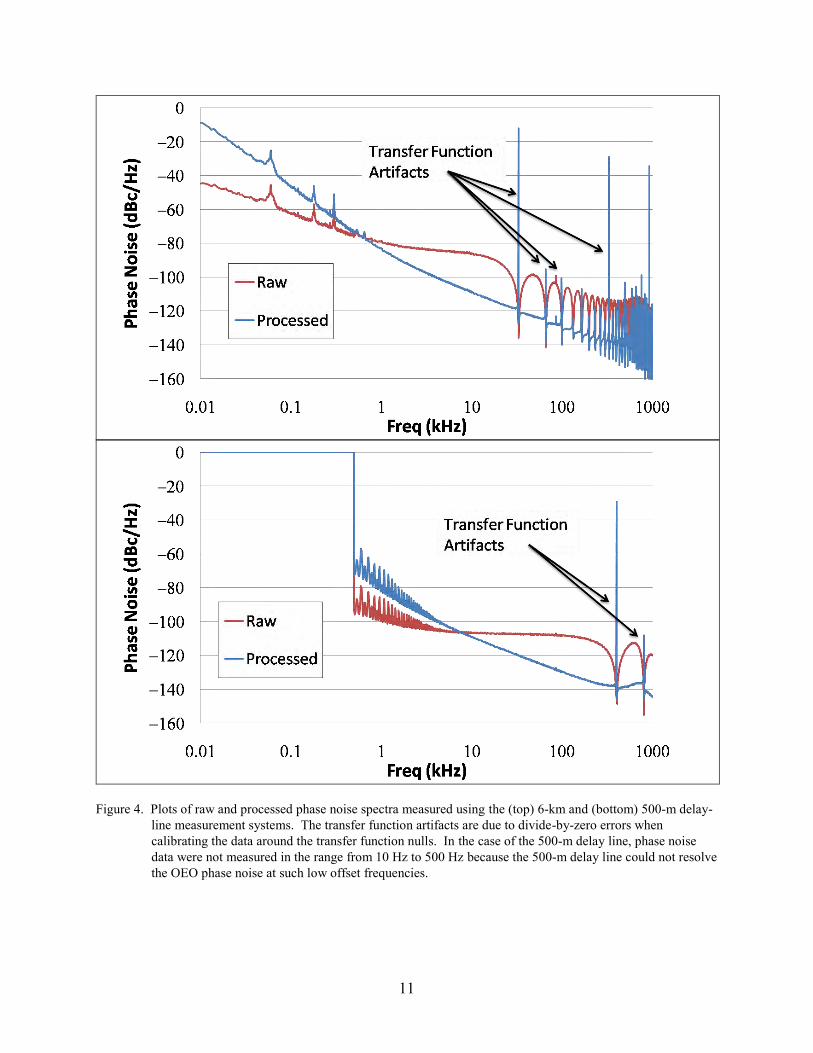
Figure 4. Plots of raw and processed phase noise spectra measured using the (top) 6-km and (bottom) 500-m delay-line measurement systems. The transfer function artifacts are due to divide-by-zero errors when calibrating the data around the transfer function nulls. In the case of the 500-m delay line, phase noise data were not measured in the range from 10 Hz to 500 Hz because the 500-m delay line could not resolve the OEO phase noise at such low offset frequencies. .....................................................................................................11
Figure 5. Stitched phase noise data obtained from combing data from the 500-m and 6-km delay-line measurements. The residual transfer function artifacts are due to the nulls of the 500-m delay line.................................................................................................................12
Figure 6. Diagram of the single-channel delay-line measurement system. The control servo is a feedback circuit designed to minimize the DC component of the mixer output. The low-pass filter used had a 1.3-MHz bandwidth. The phase shifter is electronically controlled by the servo. The FFT analyzer is a phase-sensitive detector that provides power spectrum information on the input signal. ....................................................................13
Figure 7. Comparison of ARL’s single-channel delay-line measurement data with a linear fit of NIST’s phase noise data for the same test device. ..............................................................16
Figure 8. Uncalibrated noise floor data from the delay-line measurement system, using 1-m patch cords to estimate the system noise floor.........................................................................18
Figure 9. Calibrated noise floor data from the delay-line measurement system, estimating the noise floor of the 500-m and 6-km delay-line measurement systems. ....................................18
Figure 10. A plot of the noise floor data for the combined 500-m and 6-km delay-line measurement system. ...............................................................................................................19
Figure 11. A plot of the noise floor data from the combined 500-m and 6-km delay-line measurement system. The 60-Hz harmonics are due to electrical noise from devices such as the photodiode and amplifiers that are driven by AC power. ..............................................20
Figure 12. A plot of the noise floor data from the combined 500-m and 6-km delay-line measurement system. Noise floor data are shown for the system with and without an EDFA. The laser power was 10 dBm. The optical power into the photodiode was 0 dBm without the EDFA and 11 dBm with it. ...................................................................................21

v
Figure 13. Plots of the noise floor data from the combined 500-m and 6-km delay-line measurement system. Noise floor data are shown for the system with and without an EDFA as well as with a high-power laser. The output optical powers of the low and high-power lasers were 10 and 19 dBm, respectively. The optical power into the photodiode was 0 dBm with the low-power laser, 11 dBm with the low-power laser and EDFA, and 10 dBm with the high-power laser........................................................................22
Figure 14. Plots of the noise floor data from the combined 500-m and 6-km delay line measurement system. Noise floor data are shown for the system with an ultra-low noise battery-powered current source and with a conventional AC-powered current source. ..........23
Figure 15. Plots of the noise floor data from the combined 500-m and 6-km delay-line measurement system. Noise floor data are shown for the system with conventional low-noise-figure and custom-made low-phase-noise amplifiers. ...................................................24
Figure 16. Phase noise data from a 5.6-km OEO. Noise data from a 6-km delay-line measurement system are included for comparison. The noise floor of the measurement system is higher than the OEO phase noise at several offset frequencies. ..............................25
Figure 17. A diagram of our cross-correlation delay-line measurement system. The control servo is a feedback circuit designed to minimize the DC component of the mixer output. The low-pass filter had a 1.3-MHz bandwidth. The phase shifter is electronically controlled by the servo. Channel 1 and channel 2 refer to the two delay-line measurement systems in parallel. The FFT analyzer is a dual-channel phase-sensitive detector that performs the cross-correlation on the input signals. ................................................................26
Figure 18. Comparison of the ARL cross-correlation delay-line measurement system data with phase noise data from NIST using for the same test device. The test device used for both measurements was a dielectric resonant oscillator. .........................................................29
Figure 19. Comparison of the initial implementation of the cross-correlation measurement system to the optimized single-channel measurements system. ..............................................30
Figure 20. Noise floor data from the cross-correlation measurement systems with and without isolation from EMI. ....................................................................................................31
Figure 21. Noise floor data from cross-correlation measurement systems with and without ground loops.............................................................................................................................32
vi
INTENTIONALLY LEFT BLANK.

1
1. Definition of Phase Noise
Precision oscillators are most often used as frequency or phase references. Phase noise causes the instantaneous frequency and phase of the oscillators to deviate from their nominal values. Such deviations are often the limiting factors in system performance. This study’s goal is to further the understanding of the optoelectronic oscillator’s (OEO) phase noise behavior. I begin with a precise definition of the term ―phase noise.‖ The definitions and units for phase noise used are consistent with internationally accepted standards among the radio frequency (RF) oscillator community (1).
The instantaneous output voltage of a precision oscillator can be expressed as
0 0( ) ( ) sin 2 ( ) ,V t V t t t (1)
where
0V is the nominal peak voltage amplitude,
( )t is the deviation from the nominal amplitude,
0 is the nominal frequency, and
( )t is the phase deviation from the nominal phase 02 t .
In the frequency domain, ( )f is defined as the Fourier transform of the phase deviation ( )t (1). Then the power spectral density of the phase fluctuations is given by
2 ( ).S f (2)
The units of S are rad 2 /Hz.
The standard measure for phase instabilities in the frequency domain is the phase noise, ( )f , which is defined as one half of the spectral density of the phase fluctuations:
1( ) ( ).2
f S f (3)
When expressed in decibels, the units of ( )f are dBc/Hz (dB below the carrier in a 1-Hz bandwidth). A device shall be characterized by a plot of ( )f versus discrete values of Fourier frequency f (1).
Note that there appears to be a conflict of units. ( )f has units of dBc/Hz whereas S has units
of rad 2 /Hz. The units of dBc/Hz for ( )f come from an older definition. According to the

2
older definition, ( )f is the ratio of the power in one sideband due to phase modulation by noise (for a 1-Hz bandwidth) to the total signal power (carrier plus sidebands); that is,
power density in one phase noise modulation sideband, per Hz( ) .total signal power
f (4)
I demonstrate that, under certain conditions, the two definitions of phase noise are equivalent. Looking at a simple case of a sine wave phase modulated by another sine wave, a phase modulated wave may be written as
( ) 2 sin ( ) .V t C t t (5)
Let 0( ) sin( ),t pt (6)
where is the peak phase deviation in radians and p is the phase modulation frequency. The phase modulated wave is then given by
0
0 0 1 0 1 0
2 0 2 0
( ) 2 sin ( )
2 sin sin( )
2 ( )sin ( )sin( ) ( )sin( )
( )sin( 2 ) ( )sin( 2 ) ,
V t C t t
C t pt
C J t J p t J p t
J p t J p t
(7)
where ( )nJ x is the nth order Bessel function of the first kind (2). From equation 7, we find the following:
• the carrier amplitude is 0 02 ( )CJ ,
• the first sideband amplitude is 1 02 ( )CJ (upper),
• the first sideband amplitude is 1 02 ( )CJ (lower),
• the second sideband amplitude is 2 02 ( )CJ (upper),
• the second sideband amplitude is 2 02 ( )CJ (lower), and so on.
If —which is the case for small amounts of phase noise—then we may approximate the Bessel functions as follows:
0 0
01 0
2 0 3 0 4 0
( ) 1,
( ) ,2
( ) ( ) ( ) 0.
J
J
J J J
(8)
3
The phase modulated term then becomes
0 0( ) 2 sin sin( ) sin( ) .2 2
V t C t p t p t
(9)
From equation 9, we see that for a single sideband phase modulation power of 2( / 2) rad 2 , the ratio of the modulation tone power to total signal power is simply 2( / 2) dBc.
From equation 9, we see that the ratio of the power in a single sideband induced by the phase modulation ( )t to the total signal power is given by
20
20
2 sin( )2
.4
C p t
C
(10)
So, by the old definition of phase noise given in equation 4, 20( ) / 4p , which may be
expressed in units of dBc, is measured relative to the carrier power C . From equation 6, the power spectral density of the phase modulation is given by
2
2 2 00( ) ( ) sin( ) .
2S p t pt
(11)
So, from the new definition of phase noise given in equation 3, 20( ) / 4p rad 2 /Hz.
Therefore, as long as the approximations in equation 8 hold, one may use rad 2 /Hz and dBc/Hz interchangeably. In this work, I use dBc/Hz because it emphasizes the fact that the noise powers are measured relative to the central carrier. This equivalence breaks down when
max
min
2 2( ) ( ) 0.1 radf
ft S f df , (12)
where minf and maxf are the minimum and maximum frequencies within the range of interest (1). This study uses min 10f Hz and max 1f MHz. Within this range, for the low-noise OEOs being investigating, the inequality in equation 12 does not hold, so one may use the different definitions of phase noise interchangeably. However, for offset frequencies less than 10 Hz, the OEOs phase noise increases significantly. This increased phase noise is due to the non-stationary nature of the OEO. The OEO’s round trip group-delay and gain fluctuate slowly in time, leading to greatly increased low frequency phase noise. In this domain, attempts to measure phase noise in units of dBc/Hz may lead to quantities greater than 0 dBc/Hz, which is meaningless. I avoid this low offset frequency domain in this work and so this work is not restricted to phase noise units of rad 2 /Hz.

4
2. Introduction to Carrier Suppression Noise Measurement Techniques
The phase noise powers around the OEO’s central frequency and the spurious mode powers are key quantities that limit the OEO’s performance. In order to understand the fundamental limits on these quantities, they must be accurately measured and characterized. However, the phase noise and spurious mode powers for some of our OEOs are lower than the noise floors of even the best microwave-bandwidth electrical spectrum analyzers. In addition, one is usually limited by the resolution bandwidth of the spectrum analyzer at microwave frequencies. All OEOs in this work oscillate in the 8-MHz range around 10 GHz. In the literature, the phase noise of high-Q oscillators is reported at offset frequencies as low as 1 Hz (3). In this work, I limit the data to offset frequencies of 10 Hz to 1 MHz. To reliably measure phase noise at frequencies on the order of 10 Hz, one requires a resolution bandwidth narrower than 10 Hz. In this work, I present phase noise data with resolution bandwidths as narrow as 918 mHz. A 1-Hz resolution bandwidth is difficult to obtain at 10 GHz. There are no commercially available spectrum analyzers capable of measuring 10-GHz RF signals with a 1-Hz resolution. So this attempt to measure the phase noise of OEOs is limited by both the dynamic range and the resolution bandwidth of standard spectrum analyzers. Carrier suppression techniques allow one to overcome both problems by extracting the slowly varying envelope in a fixed bandwidth around the 10-GHz carrier.
Carrier suppression measurements are made by eliminating the central carrier, which is done by mixing the central carrier with a signal at the same frequency but with a / 2 phase shift. The mixed signal is then filtered to eliminate harmonics. The resulting signal is proportional to the slowly varying phase fluctuations around the central carrier. Because the ―baseband‖ envelope ranges in frequency from DC to the corner frequency of the low-pass filter—in our case, 1.3 MHz —that is used to eliminate harmonics, one can obtain a resolution bandwidth of less than 1 Hz. Furthermore, by eliminating the central carrier, the detectors do not require the dynamic range necessary to detect both the carrier and the noise. The signal-to-noise ratio (SNR) of the OEOs can be as high as 160 dB. A HP 89410A spectrum analyzer—with a dynamic range of 110 dB—cannot measure the central carrier power and the phase noise powers at the same time. Carrier suppression allows the spectrum analyzer to measure low phase noise levels without being saturated by the carrier power.
There are two standard ways to implement a carrier suppression noise measurement: The carrier signal can be mixed with a signal from frequency standard, or the signal can be mixed with a time-delayed signal from the same oscillator (4). If a frequency standard is employed, its phase noise must be equal to or lower than that of the oscillator under test. In the case of our high- Q OEOs, one would require a second OEO or one of the few standards with phase noise levels comparable in the region of interest. One such oscillator, the Poseidon (5), is a ruby-based

5
crystal oscillator that costs in excess of $300,000.00. Rather than use an expensive frequency standard or build two versions of every OEO that tested, I chose to employ a time-delay carrier suppression system. The time delay was implemented using variable lengths of optical fiber, thereby enabling the use of a single OEO as the only active source in each of the phase noise measurements.
3. Delay-line Noise Measurement System
The delay-line technique is a homodyne detection scheme that uses a mixer and delay line to filter out the central carrier of a given input signal. The output of the homodyne detector is a baseband signal around DC proportional to the slowly varying phase fluctuations around the 10-GHz central tone. The signal to be measured is split in two by a power splitter. One portion of the signal is sent directly to one input of the mixer. The other portion experiences a delay and a phase shift before being sent into the other input of the mixer.
Figure 1 shows a schematic of the delay-line measurement system. If one writes the mixer inputs as
0 0
0 0
sin ( )and
sin ( ) ( ) ,
i
i
V t t
V t t
(13)
and is chosen so that 0 2 / 2n , where n is an integer, then the output of the mixer is
0 0
0
sin ( ) ·cos ( ) ( )
sin 2 ( ) ( ) sin( ( ) ( )
( ) ( ) ,
i i
i i i i
i i
k t t t t
k t t t t t
k t t
(14)
where one has assumed a low-pass filter to block harmonics of 0 and that the variance of the input noise
. Maintaining a / 2 phase difference between the mixer arms serves to linearize the phase-dependent output of the mixer. The constant k is the phase-to-
voltage gain of the mixer. Taking the Fourier transform of the output signal yields
( ) (1 exp( ) ( ),o ik j (15)
where ( )i is the Fourier component of the input signal phase fluctuations at frequency (6). In equation 15, I assume that the noise is stationary so that ( )t and ( )t have the same spectrum. The relative phase noise power spectrum is then proportional to the power spectrum of the mixer output given by
6
2 2( ) | ( ) | ( ),mP f k H f S f (16)
where
2 2| ( ) | 4sin ( ),H f f (17)
and f is the offset frequency of the noise relative to the 10-GHz carrier. The output signal power spectrum is equal to the input phase noise power spectrum multiplied by a frequency-dependent transfer function | ( ) |H f and an empirically determined calibration factor 2k .
Figure 1. Schematic illustration of the delay-line measurement system.
The transfer function is that of a first order finite impulse response filter (7). The delay-line measurement system is an implementation of a delay-line notch filter in which the resonant modes are rejected rather than transmitted.
Figure 2 shows a plot of the power spectral response 2
( )H f of 500-m and 6-km delay-line
measurement systems versus offset frequency. The response at low-offset frequencies scales quadratically with delay. However, the free spectral range also increases with length leading to a tradeoff between sensitivity and bandwidth. Specifically, for small offset frequencies, such that , H is proportional to 2 . Therefore, increasing the delay increases the system’s sensitivity. However, for f n , where n is an integer, we find 0H . So for a given delay,
the measurement system will have periodic nulls spaced 1/ apart in the frequency domain. Therefore, by increasing , one narrows the range of frequencies that one can effectively measure before encountering a null. So, one must perform noise measurements in a piecewise fashion, using longer delays for lower offset frequencies and shorter delays for higher offset frequencies in order to avoid nulls.

7
Figure 2. Power spectral response of 500-m and 6-km delay-line measurement systems vs. offset frequency.
4. Noise Measurement Calibration
In order to determine the phase noise of the device under test (DUT), one must determine the phase-to-voltage conversion factor k . The previous analysis dealt with the oscillating signals
( )iv t and ( )i t . However, in practice, high frequency signals are difficult to measure. It is much easier to measure the mean-square powers 2| ( ) |iv t and 2| ( ) |i t . The goal in this section is
to outline a procedure for calibrating the measurement system that relies solely on measuring the root mean square (rms) powers of the central tone of the input signal and a calibration tone.
One begins by modifying the analysis from the previous section. Starting with equation 14, the output of the mixer is
2
0 ( ) ( ) ,2 i i
Vg t t (18)
where g includes the voltage loss of the mixer (typically, –6 dB) and the gain of any amplifiers that follow immediately afterwards.
If the input noise is described by a single sinusoid given by ( ) sin( )i nt t , then the mixer output becomes

8
2
0 sin sin ( ) ,2 n n
Vg t t (19)
which may be rewritten,
20
20
20
sin sin ( )2
sin( ) sin( )cos( ) cos( )sin( )2
1 cos( ) sin( ) sin( )cos( ) .2
n n
n n n n n
n n n n
Vg t t
Vg t t t
Vg t t
(20)
The mean-square power of the mixer output is
4 222 0
4 222 2 2 20
4 22 2 20
4 22 0
( ) 1 cos( ) sin( ) sin( )cos( )4
1 cos( ) sin ( ) sin ( ) cos ( )4
1 2cos( ) cos ( ) sin ( )8
2 2cos( )8
m n n n n n
n n n n
n n n
n
VP g t t
Vg t t
Vg
Vg
4 22 20 4sin .
8 2nV
g
(21)
The analysis in section 1 for an input signal gives
0 0( ) sin sin( ) ,i nv t V t t (22)
so that the relative input phase noise power is
2
( ) .2i nS
(23)
Comparing equation 21 to equation 16 yields
2
2 2 2 200 .
4V
k g g P (24)
To determine 2k experimentally, one begins by injecting a calibration tone
0( ) sin( )c c cv t V t into one arm of the mixer. Ignoring for now the input phase noise, the inputs to the mixer are
0 0 0sin( ) sin ( )c cV t V t (25)

9
and
0 0sin ( ) .V t (26)
The mixer output becomes
0 0 0 0
00 0 0
sin sin ·sin / 2
sin 2 sin(2 ) sin .2
c c
c c c
g V t V t t
Vg V t V t t
(27)
After filtering out frequencies on the order of 02 , one is left with
0 sin .2
cc
V Vg t (28)
The mean-square power of the output is
2 2
2 20 0 ,8 2
cm c
V V PP g g P (29)
where 2 / 2c cP V is the mean-square power of the input calibration tone. From equation 29, one finds
2
0
2 .m
c
Pg
P P (30)
Substituting equation 30 into equation 24 yields
2 2 00
0
2 2· .m m
c c
P P Pk P
P P P (31)
I now summarize the calibration procedure. One begins by injecting a calibration tone into one arm of the mixer in our measurement system. Then, the mean-square powers of the calibration tone, the DUT central tone, and the measured mixer output is recorded. From these powers, one can determine the calibration factor 2k . Next, one removes the calibration tone and measures the power spectrum of the mixer output ( )mP f using a fast Fourier transform (FFT) analyzer. The relationship between the double-sideband phase noise power ( )S f and the measured spectrum
is given by
2
( )( ) .4 sin( )
mP fS f
k f
(32)

10
To obtain the single-sideband noise power one divides equation 32 by 2, yielding
2
( )( ) .8 sin( )
mP ff
k f (33)
Note that 2k is a function of the oscillator power 0P . Because the measurement system
calibration factor is a function of the input signal power, the system must be recalibrated prior to each measurement. A typical value for 2k is 20 dB, but it may fluctuate by up to 4 dB depending
on the input power from the DUT.
Figure 3 shows the ―raw‖ phase noise data ( )mP f measured using a 6-km delay-line measurement system. The nulls in the raw noise spectrum correspond to zeros in the transfer function ( )H f . Figure 4 shows raw and processed phase noise for a single OEO measured using 6-km and 500-m delay lines. The raw phase noise data are processed by dividing by
2 2| ( ) |k H f . The 6-km delay line was needed to resolve the phase noise at offset frequencies
below 10 kHz. The 500-m delay line was used to measure the phase from 10 kHz to 1 MHz. The transfer function artifacts are due to divide-by-zero errors when calibrating the data around the transfer function nulls.
Figure 3. Raw phase noise data measured using a 6-km delay-line measurement system. The nulls in the spectra correspond to zeros in the transfer function of the measurement system.
11
Figure 4. Plots of raw and processed phase noise spectra measured using the (top) 6-km and (bottom) 500-m delay-line measurement systems. The transfer function artifacts are due to divide-by-zero errors when calibrating the data around the transfer function nulls. In the case of the 500-m delay line, phase noise data were not measured in the range from 10 Hz to 500 Hz because the 500-m delay line could not resolve the OEO phase noise at such low offset frequencies.

12
Figure 5 shows the phase noise spectrum obtained by stitching together the 500-m and 6-km data. Using the two delays, the phase noise was resolved down to 10 Hz while eliminating all but two of the transfer function artifacts at higher offset frequencies.
Figure 5. Stitched phase noise data obtained from combing data from the 500-m and 6-km delay-line measurements. The residual transfer function artifacts are due to the nulls of the 500-m delay line.
5. Implementation of Delay-line Measurement System
5.1 Experimental Setup
Figure 6 shows our implementation of the delay-line measurement system. The microwave input signal is split in two using a power splitter. One portion of the signal is passed through an electrically controlled phase shifter, amplified, and then sent into the local oscillator (LO) arm of a double-balanced RF mixer. The other portion of signal is sent into the RF port of a lithium-niobate modulator. A continuous wave (CW) optical signal from a laser is modulated by the RF signal. The optical output of the modulator is passed through a length of optical fiber to induce the necessary delay . Optical fiber is used because of its low loss per unit length, allowing us to generate delays of up to 30 s with a less than 3-dB loss. In contrast, a 6-km RF waveguide would have an over 33-dB loss. The optical signal is then sent into a photodetector, the output of which is amplified and sent into the RF arm of the double-balanced mixer. The output from the intermediate frequency (IF) port of the mixer is first sent through a low pass filter with a corner frequency of 1.3 MHz to eliminate any leakage from the 10-GHz LO and RF signals arms as

13
well as second-order harmonics at 20 GHz. The filtered IF signal is then split. A small portion is fed into a feedback servo that controls the phase shifter in the RF arm. The feedback servo was designed by Dr. Craig Nelson of the Time and Frequency Metrology group at the National Institute of Standards and Technology (NIST) in Boulder, CO. Recall from section 3 that a phase shift is applied to one input of the mixer to ensure that the mixer inputs are in quadrature. The servo applies the appropriate voltage to the electrically controlled phase shifter to induce the phase shift . The servo is designed to minimize the DC component of the IF signal, thereby maintaining the two mixer arms in quadrature. When the mixer inputs are in quadrature, the IF component of the output signal is proportional to sin ( ) ( )t t , which
serves to linearize the response to small phase fluctuations. The rest of the IF signal is passed into a phase-sensitive FFT analyzer that displays the power spectral density of the IF signal. As shown in section 4, this output signal can be converted to the phase noise power spectral density of the DUT by dividing by the transfer function 2| |H and the mixer phase-to-voltage gain 2k .
Figure 6. Diagram of the single-channel delay-line measurement system. The control servo is a feedback circuit designed to minimize the DC component of the mixer output. The low-pass filter used had a 1.3-MHz bandwidth. The phase shifter is electronically controlled by the servo. The FFT analyzer is a phase-sensitive detector that provides power spectrum information on the input signal.
Note: EOM = lithium-niobate electro-optic modulator and PD = semiconductor photodetector.
14
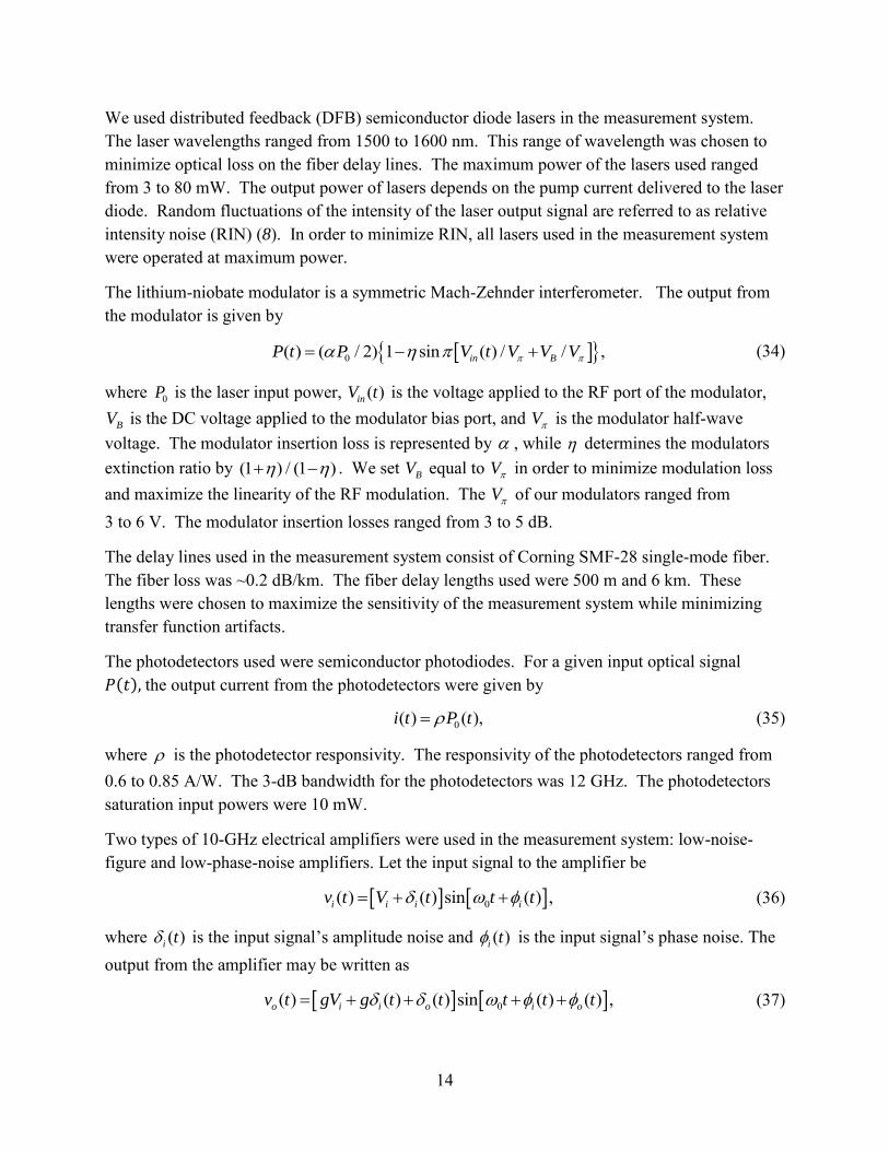
We used distributed feedback (DFB) semiconductor diode lasers in the measurement system. The laser wavelengths ranged from 1500 to 1600 nm. This range of wavelength was chosen to minimize optical loss on the fiber delay lines. The maximum power of the lasers used ranged from 3 to 80 mW. The output power of lasers depends on the pump current delivered to the laser diode. Random fluctuations of the intensity of the laser output signal are referred to as relative intensity noise (RIN) (8). In order to minimize RIN, all lasers used in the measurement system were operated at maximum power.
The lithium-niobate modulator is a symmetric Mach-Zehnder interferometer. The output from the modulator is given by
0( ) ( / 2) 1 sin ( ) / / ,in BP t P V t V V V (34)
where 0P is the laser input power, ( )inV t is the voltage applied to the RF port of the modulator,
BV is the DC voltage applied to the modulator bias port, and V is the modulator half-wave voltage. The modulator insertion loss is represented by , while determines the modulators extinction ratio by (1 ) / (1 ) . We set BV equal to V in order to minimize modulation loss and maximize the linearity of the RF modulation. The V of our modulators ranged from 3 to 6 V. The modulator insertion losses ranged from 3 to 5 dB.
The delay lines used in the measurement system consist of Corning SMF-28 single-mode fiber. The fiber loss was ~0.2 dB/km. The fiber delay lengths used were 500 m and 6 km. These lengths were chosen to maximize the sensitivity of the measurement system while minimizing transfer function artifacts.
The photodetectors used were semiconductor photodiodes. For a given input optical signal the output current from the photodetectors were given by
0( ) ( ),i t P t (35)
where is the photodetector responsivity. The responsivity of the photodetectors ranged from 0.6 to 0.85 A/W. The 3-dB bandwidth for the photodetectors was 12 GHz. The photodetectors saturation input powers were 10 mW.
Two types of 10-GHz electrical amplifiers were used in the measurement system: low-noise-figure and low-phase-noise amplifiers. Let the input signal to the amplifier be
0( ) ( ) sin ( ) ,i i i iv t V t t t (36)
where ( )i t is the input signal’s amplitude noise and ( )i t is the input signal’s phase noise. The output from the amplifier may be written as
0( ) ( ) ( ) sin ( ) ( ) ,o i i o i ov t gV g t t t t t (37)

15
where g is the amplifier voltage gain, ( )o t is the amplifier amplitude noise, and ( )o t is the amplifiers phase noise. The noise figure (NF) is a measure of the degradation of the SNR of the amplified signal (9). Let SNR i and SNRo be the input and output SNRs of the amplifier. Then the NF of the amplifier may be written as
2 2 2 2
12 2 2 2 2 2SNR ·SNR 1 .i i o
i o
i i o i
V g V
g g
(38)
Low-noise-figure amplifiers are designed to minimize the amplitude noise power 2o . The low-
noise-figure 10-GHz amplifier used in our system had a 10-dB voltage gain and a NF of 1.7 dB. The low-phase-noise amplifiers in our system had 10-dB voltage gain and a NF of 6 dB. However, the low-phase-noise amplifiers were specifically designed to minimize o the amplifier-induced phase noise. A few practical issues were discovered when constructing the delay-line noise measurement system. Both the low-noise-figure and low-phase-noise amplifiers had a 20-dB saturation power.
It is crucial to drive both arms of the double-balanced mixer to saturation in order to maximize phase noise sensitivity and eliminate amplitude noise corruption. When the mixer input ports are saturated, slight fluctuations in the signal amplitude do not alter the output voltage. The mixers in this setup required at least a 7-dBm input power at 10 GHz to saturate each arm. I found that input powers of 10 dBm 3 dB were most effective for maximizing phase noise sensitivity.
5.2 System Validation
To validate the measurement system, I received assistance from Dr. David Howe, Dr. Archita Hati, and Dr. Craig Nelson of the Time and Frequency Metrology group at NIST in Boulder, CO. A 10-GHz dielectric resonant oscillator (DRO) was used as a test device. Its phase noise was measured at NIST using a digital phase-locked-loop measurement system with an ultra-low-phase-noise ―Poseidon‖ oscillator (5) used as a standard. The DRO was then measured using the delay-line measurement system at the U.S. Army Research Laboratory (ARL). For the overlapping range of measured frequencies—10 Hz to 10 kHz—there was very good agreement between both measurement systems. Figure 7 shows the DRO phase noise measured at ARL versus a linear fit on a log-log scale of the NIST data. The noise spikes seen in the ARL measurement are harmonics of the 60-Hz tone from the AC power supply that powered the measurement system’s electronics.

16
Figure 7. Comparison of ARL’s single-channel delay-line measurement data with a linear fit of NIST’s phase noise data for the same test device.
Figure 7 shows that ARL’s measurement system is capable of accurately measuring noise levels on the same order as the DRO. However, an estimate of the minimum noise level the ARL system can measure is also required. The components in the measurement system all generate noise. If the total noise generated by the system is greater than the noise of the DUT, then the system cannot measure the phase noise of the DUT. The noise floor of the measurement system is defined as the lowest DUT noise level that can be accurately measured by the system. In order to investigate the phase noise of the OEOs in this study, a measurement system is required whose noise floor is lower than the noise of any OEO tested. Sections 5.3 and 5.4l describe how I estimated the noise floor of the ARL measurement system.
5.3 Noise Floor Estimation
I have demonstrated the importance of ensuring that the ARL phase noise measurement system is capable of resolving the OEOs phase noise. One also must know, for a given phase noise measurement system, the lowest phase noise that can be measured in a DUT. One can think of the system noise as a noise floor. DUT noise levels below this floor cannot be measured accurately by the measurement system.
So how does one measure the system noise floor? One may be tempted to do so by simply turning off the DUT and recording whatever noise is measured. Unfortunately, this approach inevitably underestimates the system noise floor. Recall that this system relies on carrier suppression at the mixer to measure the DUT’s phase noise. Carrier suppression requires an input power into the LO arm of the mixer that is sufficient to drive the mixer diodes into

17
saturation. In saturation, the mixer diodes’ second-order nonlinearity serves to multiply the LO and RF input signal. Since the LO and RF arms are / 2 out of phase, the result is a large signal at their difference frequency. It is this baseband signal that is measured. However, without a sufficiently powerful signal into the LO arm, the mixer’s second-order nonlinearity is greatly diminished. In this case, the mixer simply acts as a power-combiner. There is no mixing of the LO and RF signal, and consequently, there is no baseband signal for us to measure. Hence, one must have a technique that allows one to leave the DUT on and connected to the measurement system.
One such method was proposed by Rubiola et al. (6). The Rubiola method replaces the long delay lines in the measurement system with short delays with similar loss. Recall that the transfer function of the measurement system is given by
2 24sin ( ) .o iS k f S (39)
In the limit where 0 , the measured output oS should go to 0. Therefore, if one sets the
measurement system delay to zero, any output signal measured will be the system noise. Note, however, that one cannot set the measurement system delay to precisely 0. The lasers and photodiodes in the measurement system all have fiber pigtails that are approximately 1 m long. Also, the electrical amplifiers, mixers, phase shifters, and filters all induce some small group delay in the DUT signal. So, while one can reduce significantly, one cannot eliminate it entirely. Nevertheless, going from a of 6 km to one of approximately 6 m will reduce the DUT signal by 60 dB. Therefore, whatever signal one measures is either the DUT’s phase noise attenuated by 60 dB or the noise floor of the measurement system. The Rubiola method provides an upper bound of the measurement system noise floor, so whatever one measures via the Rubiola method will be greater than or equal to the system noise floor. It is important to use a low-noise DUT so that one does not excessively overestimate the system noise floor.
I implemented the Rubiola method by replacing the fiber spools in the cross-correlation delay-line measurement system with 1-m fiber patch cords. Optical attenuators are attached to the 1-m patch cords so that they have the same loss as the spools. Then the raw phase noise data are collected. Figure 8 shows raw noise floor data from the ARL measurement system. The measured signal represents the lowest raw signal power that the measurement system can resolve. To obtain the lowest DUT phase noise that the system can resolve, one must divide by the transfer functions of the 500-m and 6-km delay-lines length that are used. In other words, having measured the raw noise floor with a of 6 m, one divides by the transfer function using a of 2.5 or 30 s to determine the noise floor of a 500-m or 6-km measurement system using the same components. Figure 9 shows the estimated noise floor of the 500-m and 6-km delay-line measurement systems. The plots were generated by dividing the raw noise floor data by the transfer function of the respective delay lines. Note that for offset frequencies below 20 kHz, the noise floor for the 6-km delay line is lower than that of the 500-m delay line. However, above 20 kHz, the 500-m delay-line system proves superior because it has few transfer function

18
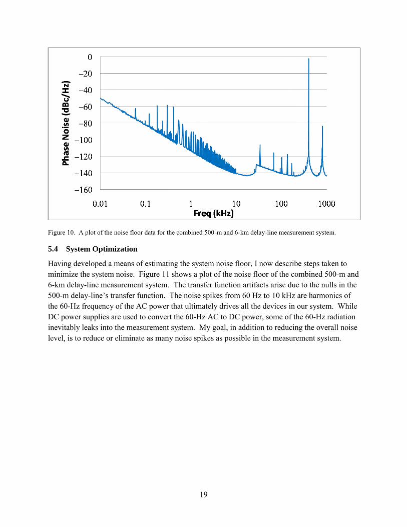
artifacts. To obtain the best performance, one must combine phase noise data from both the 500-m and 6-km delay-line measurement systems. Figure 10 shows the noise floor of the combined system.
Figure 8. Uncalibrated noise floor data from the delay-line measurement system, using 1-m patch cords to estimate the system noise floor.
Figure 9. Calibrated noise floor data from the delay-line measurement system, estimating the noise floor of the 500-m and 6-km delay-line measurement systems.
19
Figure 10. A plot of the noise floor data for the combined 500-m and 6-km delay-line measurement system.
5.4 System Optimization
Having developed a means of estimating the system noise floor, I now describe steps taken to minimize the system noise. Figure 11 shows a plot of the noise floor of the combined 500-m and 6-km delay-line measurement system. The transfer function artifacts arise due to the nulls in the 500-m delay-line’s transfer function. The noise spikes from 60 Hz to 10 kHz are harmonics of the 60-Hz frequency of the AC power that ultimately drives all the devices in our system. While DC power supplies are used to convert the 60-Hz AC to DC power, some of the 60-Hz radiation inevitably leaks into the measurement system. My goal, in addition to reducing the overall noise level, is to reduce or eliminate as many noise spikes as possible in the measurement system.

20
Figure 11. A plot of the noise floor data from the combined 500-m and 6-km delay-line measurement system. The 60-Hz harmonics are due to electrical noise from devices such as the photodiode and amplifiers that are driven by AC power.
I begin by investigating the effect of optical power on the noise floor of the measurement system. Figure 11 shows the noise floor of a measurement system in which a 10-dBm laser was used. The lithium-niobate modulator used had a 5-dB insertion loss. The lithium-niobate modulator is biased such that the mean power after the modulator is half the input power. Finally, the 6-km delay line has an additional 2-dB loss. While the noise floor estimated did not include the 6-km spool, it included a 1-m patch cord with 2-dB of attenuation to match the attenuation of the 6-km delay line. So the mean optical power that went into the photodiode was 0 dBm. I investigate the effect of introducing optical power into the photodiode by adding an erbium-doped fiber amplifier (EDFA) after the fiber spool. The EDFA had a 13-dB gain, so that the optical power afterwards was 13 dBm. However, EDFAs generate large amounts of spontaneous emission noise over a broad bandwidth (10). This amplified spontaneous emission noise can beat with the optical signal at a photodiode to create broadband RF noise (11). To prevent this signal-noise beating, I placed an optical bandpass filter with a 1-nm bandwidth after the EDFA. Due to the 2-dB insertion loss of the optical filter, the final optical power into the photodiode was 11 dBm. Figure 12 shows the noise floor of the measurement system with and without the EDFA. With the EDFA, there is a minor reduction in the minimum noise of the system. The reduction was approximately 2 dB at a 1-kHz offset frequency. However, there was a dramatic reduction in the level of the 60-Hz harmonics of the system. The 60-Hz harmonics at 1 kHz were reduced by approximately 10 dB, while those at 10 kHz were reduced by 6 dB. This reduction suggests that the 60-Hz harmonics were due in part to electrical noise in the photodiode. Increasing the optical power into the photodiode reduced the relative contribution from the photodiode electrical noise.

21
Figure 12. A plot of the noise floor data from the combined 500-m and 6-km delay-line measurement system. Noise floor data are shown for the system with and without an EDFA. The laser power was 10 dBm. The optical power into the photodiode was 0 dBm without the EDFA and 11 dBm with it.
Next, I removed the EDFA and optical filter and then replaced the 10-mW DFB laser with a 100-mW DFB laser. The optical power from the laser was 20 dBm. The power after the modulator was 12 dBm and the power into the photodiode after the attenuating patch cord was 10 dBm. The high-power laser allowed me to provide approximately the same optical power into the photodiode as the combination of the low-power laser and the EDFA. However, the high-power laser provided this power without spontaneous emission noise from an EDFA. Figure 13 shows the noise floor of the measurement system with the low-power laser, the low-power laser and EDFA, and the high-power laser. The system with the high-power laser had the same noise floor at 1 kHz as the system with the EDFA. However, the noise floor with the high-power laser was 7 dB lower than with the EDFA at an offset frequency of 10 kHz, suggesting that the effect of the EDFA spontaneous emission noise is strongest at high offset frequencies. In addition, the high-power laser reduced the 60-Hz harmonics by over 10 dB relative to the EDFA.

22
Figure 13. Plots of the noise floor data from the combined 500-m and 6-km delay-line measurement system. Noise floor data are shown for the system with and without an EDFA as well as with a high-power laser. The output optical powers of the low and high-power lasers were 10 and 19 dBm, respectively. The optical power into the photodiode was 0 dBm with the low-power laser, 11 dBm with the low-power laser and EDFA, and 10 dBm with the high-power laser.
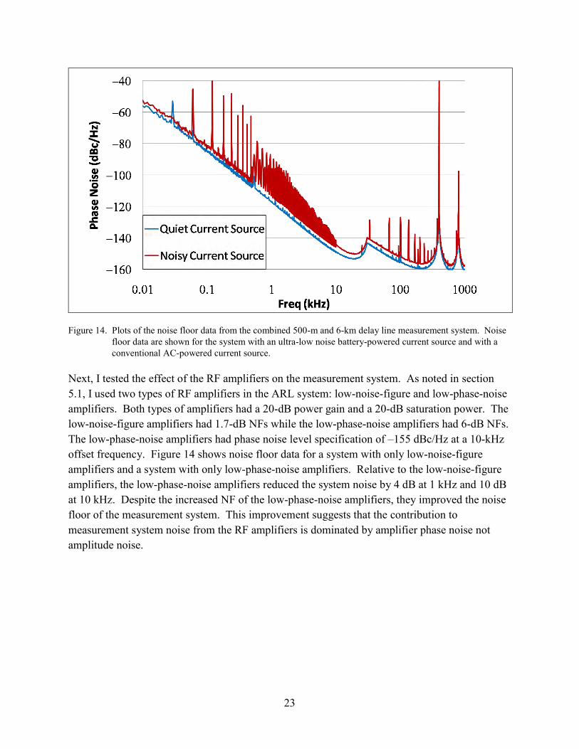
While the high-power laser outperformed the combination of the low-power laser and EDFA, care must be taken to properly drive the laser. In all of the above measurements, the laser was driven with a battery-powered ultra-low-noise current source. The battery-powered source provides drive currents free of 60-Hz harmonics to the laser diode. To test the effect of the laser current source on the system noise floor, I replaced the ultra-low-noise source with a conventional AC-powered laser-diode current driver. Figure 14 shows the system noise floor using both current sources. The conventional current source increased the noise floor by 2 to 3 dB at all offset frequencies. The conventional driver also increased the 60-Hz harmonics by up to 45 dB. Thus, the low-noise laser current sources are essential to creating a low-noise measurement system.
23
Figure 14. Plots of the noise floor data from the combined 500-m and 6-km delay line measurement system. Noise floor data are shown for the system with an ultra-low noise battery-powered current source and with a conventional AC-powered current source.
Next, I tested the effect of the RF amplifiers on the measurement system. As noted in section 5.1, I used two types of RF amplifiers in the ARL system: low-noise-figure and low-phase-noise amplifiers. Both types of amplifiers had a 20-dB power gain and a 20-dB saturation power. The low-noise-figure amplifiers had 1.7-dB NFs while the low-phase-noise amplifiers had 6-dB NFs. The low-phase-noise amplifiers had phase noise level specification of –155 dBc/Hz at a 10-kHz offset frequency. Figure 14 shows noise floor data for a system with only low-noise-figure amplifiers and a system with only low-phase-noise amplifiers. Relative to the low-noise-figure amplifiers, the low-phase-noise amplifiers reduced the system noise by 4 dB at 1 kHz and 10 dB at 10 kHz. Despite the increased NF of the low-phase-noise amplifiers, they improved the noise floor of the measurement system. This improvement suggests that the contribution to measurement system noise from the RF amplifiers is dominated by amplifier phase noise not amplitude noise.

24
Figure 15. Plots of the noise floor data from the combined 500-m and 6-km delay-line measurement system. Noise floor data are shown for the system with conventional low-noise-figure and custom-made low-phase-noise amplifiers.
Optimizing the noise measurement system reduced the system noise floor to –115 dBc/Hz at 1 kHz, –148 dBc/Hz at 10 kHz, and –160 dBc/Hz at 200 kHz. However, these noise floor levels are still too high to measure the phase noise in all of the OEOs in this study. Figure 16 shows phase noise data from a 5.6-km single-loop OEO. Included in the figure is the noise floor data from the 6-km delay-line measurement system. The OEO phase noise is lower than the measurement system noise floor below 70 Hz, from 120 to 280 Hz, and from 450 Hz to 2 kHz. To accurately measure the phase noise of the lowest-noise OEOs in this study, I built a cross-correlation delay-line measurement system with noise-floor levels lower than any OEO in this study. Section 6 describes the implementation of the cross-correlation delay-line measurement system.

25
Figure 16. Phase noise data from a 5.6-km OEO. Noise data from a 6-km delay-line measurement system are included for comparison. The noise floor of the measurement system is higher than the OEO phase noise at several offset frequencies.
6. Cross-correlation Delay Line Measurement System
6.1 Experimental Setup
With this delay-line measurement system, I was able to measure phase noise powers as low as –115 dBc/Hz at a 1-kHz offset frequency. However, ARL OEOs are capable of producing RF tones at 10 GHz with even lower phase noise levels. To properly measure such signals, I had to improve the sensitivity of this measurement system. Cross-correlation delay-line measurement systems have been to show to have lower noise floors than single channel delay-line systems (12). I constructed a cross-correlation system that is capable of measuring OEO phase noise levels as low as –140 dBc/Hz at 1 kHz offset frequency. Figure 17 shows a schematic of the cross-correlation measurement system.

26
Figure 17. A diagram of our cross-correlation delay-line measurement system. The control servo is a feedback circuit designed to minimize the DC component of the mixer output. The low-pass filter had a 1.3-MHz bandwidth. The phase shifter is electronically controlled by the servo. Channel 1 and channel 2 refer to the two delay-line measurement systems in parallel. The FFT analyzer is a dual-channel phase-sensitive detector that performs the cross-correlation on the input signals.
The cross-correlation measurement system consists of two delay-line measurement systems in parallel. The oscillator signal is first split in two and then sent to each delay-line system. The output of the delay-line systems are then sent into a dual-channel FFT analyzer. The FFT analyzer performs a cross correlation on the frequency spectrum of both channels. As shown in section 3, ( )oS f can be obtained from the output of each delay-line system. In practice,
however, the delay-line system output will include noise from the measurement system itself. As shown in section 5.4, sources of system noise include the laser driver, photodetector, and RF

27
amplifiers. The cross-correlation system suppresses this noise by taking advantage of the uncorrelated nature of the system noise sources.
6.2 Cross-correlation
For two uncorrelated signals a(t) and b(t), we have
( )· ( ) 0.a t b t (40)
The assumption is that the output from each delay-line system consists of combination of a portion proportional to the phase noise of the DUT. The other portion consists of system noise specific to that particular delay-line channel. Let 1,2 ( )V t be the portion of the output from channels 1 and 2 that is proportional to the phase noise of the DUT. Let 1,2 ( )t be the portion of
the output from channels 1 and 2 that is due to system noise from each channel. Then, the voltages 1( )V t and 2 ( )V t will be correlated, whereas 1( )t and 2 ( )t will be uncorrelated. Therefore, calculating the cross correlation of the outputs of channels 1 and 2 yields
*
1 1 2 2( ) ( ) · ( ) ( ) .V t t V t t (41)
When dealing with discrete samples, equation 41 becomes
*1 1 2 2
0
* * * *1 2 1 2 2 1 1 2
0
* * * *1 2 1 2 2 1 1 2
1 [ ] [ ] · [ ] [ ]
1 [ ]· [ ] [ ]· [ ] [ ]· [ ] [ ]· [ ]
· · · ·,
N
n
N
n
V n n V n nN
V n V n V n n V n n n nN
N V V N V N V N
N
(42)
where N is the number of averages taken and x is the root-mean value of x n . It is assumed that the series 1,2[ ]V n and 1,2[ ]n are all stationary. The cross-correlation system noise is defined
as
* * *1 2 2 1 1 2
system
* * *1 2 2 1 1 2
· · ·
· · · ,
N V N V N
N
V V
N
(43)
which is the output of the cross-correlation system that is due to the system noise in each measurement channel. Then, equation 42 becomes
system*1 2· .V V
N
(44)

28
Equation 44 shows that the system noise is suppressed by a factor of 1/ N as long as the system remains stationary. Typically, one can only expect the system to remain stationary for approximately 10,000 averages (12). For 10,000N , one sees little further reduction in the measurement system output. The stationary limit implies that one can achieve at best a 20-dB system noise reduction by implementing a cross-correlation measurement system.
6.3 System Calibration and Validation
One must calibrate the output of the cross-correlation measurement system in order to extract useful phase noise information from it. Equation 44 shows that the signal portion of the output from the cross-correlation measurement system is
*1 2· ,V V (45)
where 1V and 2V are the output signals from channels 1 and 2, respectively. Let 1( )V f and
2 ( )V f be the complex Fourier spectra of the output signals from channel 1 and 2. Then, from section 3, one may write
1 1
2 2
( ) ( ) ( ),
( ) ( ) ( ),
V f f k H f
V f f k H f
(46)
where 1k and 2k are the calibration factors for channels 1 and 2 and ( )f is the DUT phase
noise spectrum. From equations 45 and 46, one finds that the output power spectrum from the cross-correlation measurement system is
1 22 2
1 2
2
1 2
( ) ( ) ( )
( )
( )
( ) . ( )
mP f V f V f
f k k H f
k k H f S f
(47)
Comparing equation 47 to equation 16, one finds that the effective calibration factor of the cross-correlation measurement system is
21 2 ,ck k k (48)
which is the geometric mean of the calibration factors of the individual channels.
Figure 18 shows a validation of our cross-correlation measurement system with data from NIST. As with the single-channel measurement system, the same test device—a dielectric resonant oscillator—was measured using both systems. There is extremely good agreement over the entire measurement range.

29
Figure 18. Comparison of the ARL cross-correlation delay-line measurement system data with phase noise data from NIST using for the same test device. The test device used for both measurements was a dielectric resonant oscillator.
6.4 System Optimization
The cross-correlation measurement system employs the same optimization measures used in the single-channel measurement system. High-power lasers are used in both measurement channels that provide 10 dBm of optical power to the photodetectors. I used low-phase-noise amplifiers and low-noise battery-powered current sources in both channels. Figure 19 shows noise floor data for both single-channel and cross-correlation measurement systems. The cross-correlation system noise is lower than that of the single-channel system; however, the noise reduction is not as great as the 20-dB reduction predicted by the theory. There is significantly more noise structure in the cross-correlation noise floor. I observed 60-Hz harmonics in the frequency range from 500 Hz to 10 kHz that rise as much as 15 dB above the surrounding noise level.

30
Figure 19. Comparison of the initial implementation of the cross-correlation measurement system to the optimized single-channel measurements system.
I next worked to isolate the electro-magnetic interference (EMI) from measurement system. The ambient EMI level was lower than the noise floor of the single-channel measurement system. However, in the case of the cross-correlation system, ambient EMI levels were large enough to deteriorate the system performance. EMI originated primarily from power supplies, signal generators, spectrum analyzers, and other devices with rectifiers and transformers. These devices radiate electromagnetic waves that can induce IF signals in the measurement system. We found that reducing EMI required ensuring that the FFT analyzer and both channels of the measurement system were at least 0.5 m away from any high-power electrical device. Also, shielded power supply and RF cables reduced the EMI in the measurement system. Figure 20 shows noise floor data with and without EMI isolation. The electrical noise—particularly 60 Hz harmonics—were reduced by up to 7 dB.

31
Figure 20. Noise floor data from the cross-correlation measurement systems with and without isolation from EMI.
Further improvement in the measurement system was obtained by eliminating ground loops and cross-talk between the two measurement system channels. Ground loops occur in a system when different parts of a circuit that are supposed to be at the same potential—typically, ground—are at slightly different potentials. When different parts of a circuit experience different grounds, unintended currents can flow between these points which greatly increase the system noise. To eliminate ground loops within the measurement system circuits, I carefully connected all the negative terminals of the devices to ground using high-gauge shielded cable. Similar problems can occur between circuits that should not be connected. Channels 1 and 2 should be isolated as much as possible to ensure that they remain uncorrelated. In early experiments, the two channels were clamped to the same optical table. The metal surface of the optical table acted as a conductor that transmitted low-frequency currents between both channels. Since the devices in each channel were connected to different power supplies—and consequently were at different grounds—unwanted currents flowed between both channels.
Even when both channels were mounted on separate platforms that were isolated from the optical table, the RF cables that connected both channels to the DUT acted as paths for DC and IF currents to travel between the two channels. I solved this problem by applying DC blocks to the RF inputs of both channels. A DC block is a capacitor circuit designed to act as a short to high-frequency signals but to block low-frequency signals. The DC blocks used allowed the 10-GHz signal through but blocked frequencies below 10 MHz from traveling between the measurement system channels. Figure 21 shows the result of eliminating ground loops and inter-channel cross-talk from the measurement system. Electrical noise in the form of 60-Hz harmonics was

32
reduced by a factor of up to 7 dB. The resulting measurement system has a noise floor of –140 dBc/Hz at 1 kHz. To my knowledge, that is lower than the phase noise of any 10 GHz oscillator that is currently published in the literature or commercially available (3).
Figure 21. Noise floor data from cross-correlation measurement systems with and without ground loops.
7. Conclusion
Having optimized our measurement system by eliminating EMI and ground loops, I succeeded in the goal of creating a system that would allow one to measure the phase noise of any OEO in this study. The resulting cross-correlation delay-line measurement system was a crucial tool in the study that follows. It provided accurate phase noise and spurious mode information on all the oscillators constructed, allowing the physics of the single-loop and injection-locked OEOs to be captured.

33
8. References
1. IEEE Standard Definitions of Physical Quantities for Fundamental Frequency and Time Metrology - Random Instabilities, IEEE Std. 1139–1999, 1999.
2. Robins, W. P. Phase Noise in Signal Sources: Theory and Applications. ser. IEEE
Telecommunications Series. London, England: Institution of Engineering and Technology
(IET) 1984, 9, 9–12.
3. Howe, D. A.; Hati, A. Low-noise X-band Oscillator and Amplifier Technologies: Comparison and Status. In Proceedings of the Joint IEEE International Frequency Control
Symposium and Precise Time and Time Interval (PTTI) Systems and Applications Meeting, Vancouver, Canada, Aug. 2005, 481–487.
4. Li, J.; Ferre-Pikal, E.; Nelson, C.; Walls, F. L. Review of PM and AM Noise Measurement Systems. in Proceedings of the IEEE International Frequency Control Symposium, Los Angeles, CA, Jun. 1998, 197–200.
5. Mossammaparast, M.; McNeilage, C.; Stockwell, A.; Searls, J. H.; Suddaby, M. E. Low Phase Noise Division from X-band to 640 MHz. In Proceedings of the IEEE International
Frequency Control Symposium and PDA Exhibition, New Orleans, LA, May 2002, 685–689.
6. Rubiola, E.; Salik, E.; Huang, S.; Yu, N.; Maleki, L. Photonic-delay Technique for Phase-Noise Measurement of Microwave Oscillators. J. Opt. Soc. Am. B 2005, 22 (5), 987–997.
7. Gookin, D. M.; Berry, M. H. Finite Impulse Response Filter with Large Dynamic Range and High Sampling Rate. Appl. Opt. 1990, 29 (8), 1061–1062.
8. Lee, W.; Choi, M.; Izadpanah, H.; Delfyett, P. Relative Intensity Noise Characteristics in a Frequency Stabilized Mode-locked Semiconductor Laser System. In Proceedings of the
Conference on Lasers and Electro-Optics and the Conference on Quantum electronics and
Laser Science (CLEO/QELS '06), Long Beach, CA, May 2006, pp. 1–2.
9. Paterson, W. L. Multiplication and Logarithmic Conversion by Operational Amplifier-transistor Circuits. Review of Scientific Instruments 1963, 34 (12), 1311–1316.
10. Qiao, L.; Vella, P. J. ASE Analysis and Correction for EDFA Automatic Control. J. Lightw.
Technol. Jun. 2007, 25 (3), 771–778.
11. Rebola, J. L.; Cartaxo, A.V.T. Power Penalty Assessment in Optically Preamplified Receivers with Arbitrary Optical Filtering and Signal-dependent Noise Dominance. J.
Lightw. Technol. Mar. 2007, 20 (3), 401–408.

34
12. Walls, W. F. Cross-correlation Phase Noise Measurements. In Proceedings of the IEEE
Frequency Control Symposium, Miami, FL, May 1992, pp. 257–261.

35
List of Symbols, Abbreviations, and Acronyms
ARL U.S. Army Research Laboratory
CW continuous wave
DFB distributed feedback
DRO dielectric resonant oscillator
DUT device under test
EDFA erbium-doped fiber amplifier
EMI electro-magnetic interference
EOM electro-optic modulator
FFT fast Fourier transform
IF intermediate frequency
LO local oscillator
NF noise figure
NIST National Institute of Standards and Technology
OEO opto-electronic oscillator
PD photodetector
RF radio frequency
RIN relative intensity noise
rms root mean square
SNR signal-to-noise ratio

36
No. of
Copies Organization
1 PDF ADMNSTR DEFNS TECHL INFO CTR ATTN DTIC OCP 8725 JOHN J KINGMAN RD STE 0944 FT BELVOIR VA 22060-6218 10 US ARMY RSRCH LAB ATTN IMNE ALC HRR MAIL AND RECORDS MGMT ATTN RDRL CIO LL TECHL LIB ATTN RDRL CIO MT TECHL PUB ATTN RDRL SE G WOOD ATTN RDRL SE K ALIBERTI ATTN RDRL SE P GILLESPIE
ATTN RDRL SEE M O OKUSAGA ATTN RDRL SEE M W ZHOU ATTN RDRL SEE M M STEAD ATTN RDRL SEE M L STOUT
ADELPHI MD 20783-1197 TOTAL: 11 (9 HCS, 1 PDF)