pci-/cpci-/lpci-/ lpcie-725x series - acceed · pci-/cpci-/lpci-/ lpcie-725x series ... but also...
TRANSCRIPT
Advance Technologies; Automate the World.
Manual Rev. 2.03
Revision Date: June 24, 2008
Part No: 50-11038-1000
PCI-/cPCI-/LPCI-/LPCIe-725X Series
8-CH Relay Output &8-CH Isolated Digital Input Cards
User’s Manual

Copyright 2008 ADLINK TECHNOLOGY INC.
All Rights Reserved.
The information in this document is subject to change without prior notice in order to improve reliability, design, and function and does not represent a commitment on the part of the manufacturer.
In no event will the manufacturer be liable for direct, indirect, spe-cial, incidental, or consequential damages arising out of the use or inability to use the product or documentation, even if advised of the possibility of such damages.
This document contains proprietary information protected by copy-right. All rights are reserved. No part of this manual may be repro-duced by any mechanical, electronic, or other means in any form without prior written permission of the manufacturer.
Trademarks
Product names mentioned herein are used for identification pur-poses only and may be trademarks and/or registered trademarks of their respective companies.
Getting Service from ADLINKCustomer Satisfaction is top priority for ADLINK Technology Inc. Please contact us should you require any service or assistance.
ADLINK TECHNOLOGY INC.Web Site: http://www.adlinktech.comSales & Service: [email protected]: +886-2-82265877FAX: +886-2-82265717Address: 9F, No. 166, Jian Yi Road, Chungho City,
Taipei, 235 Taiwan
Please email or FAX this completed service form for prompt and satisfactory service.
Company Information
Company/OrganizationContact PersonE-mail AddressAddressCountryTEL FAX:Web Site
Product InformationProduct Model
EnvironmentOS:M/B: CPU:Chipset: Bios:
Please give a detailed description of the problem(s):


Table of Contents i
Table of ContentsTable of Contents..................................................................... i
List of Tables.......................................................................... iii
List of Figures ........................................................................ iv
1 Introduction ........................................................................ 11.1 Features............................................................................... 21.2 Applications ......................................................................... 21.3 Specifications....................................................................... 3
Digital input ..................................................................... 3Relay Output ................................................................... 3General Specifications .................................................... 4Power Consumption ....................................................... 4
1.4 Software Support ................................................................. 5Windows Drivers ............................................................. 6Linux Drivers ................................................................. 11Third-party Software Support ........................................ 12VEE™ Interface for ADLINK DAQ Cards ..................... 14Componentware/ActiveX Control .................................. 15Applications for Test and Measurement ....................... 16
2 Installation ........................................................................ 172.1 Unpacking Checklist .......................................................... 172.2 PCB Layout........................................................................ 18
PCI-7250 PCB Layout .................................................. 18cPCI-7252 PCB Layout ................................................. 19LPCI-7250 PCB Layout ................................................ 20LPCIe-7250 PCB Layout .............................................. 21
2.3 Input Signal Jumper Setting............................................... 222.4 Hardware Installation Outline............................................. 23
PCI Configuration ......................................................... 23PCI Slot Selection ......................................................... 23Installation Procedures ................................................. 23
2.5 Device Installation for Windows Systems .......................... 242.6 Connector Pin Assignments .............................................. 24
PCI-7250/51 Pin Assignment ........................................ 24cPCI-7252 Pin Assignment ........................................... 26
ii Table of Contents
LPCI/LPCIe-7250 CN1 Pin Assignment ....................... 272.7 PCI-7250 and PCI-7251 Connection ................................. 28
3 Registers............................................................................ 293.1 PCI PnP Registers ............................................................. 293.2 I/O Address Map................................................................ 303.3 Relay Output and Readback Registers.............................. 303.4 Isolation Input Registers .................................................... 31
4 Operation Theory .............................................................. 334.1 Using Relay Output............................................................ 334.2 Using Isolated Input ........................................................... 35
Appendix ................................................................................ 37Relay Contact Protection Circuits ...................................... 37
RC Circuit ..................................................................... 37Diode Circuit ................................................................. 38Diode & Zener diode Circuit .......................................... 39Varistor Circuit .............................................................. 39

List of Tables iii
List of TablesTable 1-1: Digital Input Specifications ....................................... 3Table 1-2: Relay Output Specifications ..................................... 3Table 1-3: General Specifications .............................................. 4Table 1-4: Power Consumption Specifications .......................... 4Table 2-1: Jumpers and DI Channels ...................................... 22Table 2-2: Input Signal Selection Jumper Settings .................. 22Table 2-3: CN1 - PCI-7250/51 Pin Assignment ....................... 25Table 2-4: CN1 - cPCI-7252 Pin Assignment .......................... 26Table 2-5: LPCI/LPCIe-7250 CN1 Pin Assignment ................. 27Table 3-1: PCI-7250 Address Map with PCI-7251 Installed .... 30Table 3-2: cPCI-7252 Address Map ........................................ 30Table 3-3: LPCI/LPCIe-7250 Address Map ............................. 30Table 3-4: Data Format of Relay Output and Readback Status Reg-
isters ....................................................................... 31Table 3-5: Relay Output ........................................................... 31

iv List of Figures
List of FiguresFigure 2-1: PCI-7250 Layout...................................................... 18Figure 2-2: cPCI-7252 Layout .................................................... 19Figure 2-3: LPCI-7250 PCB Layout ........................................... 20Figure 2-4: LPCIe-7250 PCB Layout ......................................... 21Figure 2-5: CN1 - D Type Connector ......................................... 24Figure 2-6: Connection between PCI-7250 and PCI-7251......... 28Figure 4-1: Form C Relay........................................................... 33Figure 4-2: Form A Relay........................................................... 34Figure 4-3: PCI-7250 Differential Input Circuit ........................... 35Figure 4-4: cPCI-7252 Isolated Input Circuit .............................. 35Figure 4-5: LPCI/LPCIe-7250 Differential Input Circuit .............. 36

Introduction 1
1 IntroductionThe PCI-7250/7251, cPCI-7252, LPCI-7250 and LPCIe-7250 8-CH Relay Output & 8-CH Isolated Digital Input Cards are basic Digital I/O cards for PCI bus compliant computers used in indus-trial applications.
This PCI-7250/7251 provide 8 relay actuators and 8 opto-isolated digital inputs. Of the eight relays, four are Form C (R0~R3) and four are Form A (R4~R7). The cPCI-7252 provides 8 relay actua-tors and 16 opto-isolated digital inputs; all relays are Form C. The LPCI-7250 and LPCIe-7250 provide 8 relay actuators and 8 opto-isolated digital inputs; all relays are Form C. They are very suited for constant ON/OFF control devices. For convenience the above models will be referred to as PCI-725X in this manual.
All digital input channels are isolated and suitable applications in noisy environment. For identical non-polarized opto-isolated digital input channels, switching can be carried out using AC-filtered or non-AC-filtered channels.
PCI-7250 is equipped with LEDs to reflect the status of each relay output. When a relay is energized, its corresponding LED will turn ON, otherwise it is OFF.
The relay outputs and digital inputs are controlled by two bytes of I/O addresses. When a bit is read or written, its output status will be controlled, or its input status will be monitored. The I/O signals are routed through to a 37-pin D-type or a 50-pin SCSI-II connec-tor.

2 Introduction
1.1 FeaturesThe PCI-725X Relay Actuator and D/I cards provide the following advanced features:
32-bit PCI-Bus, Plug and Play (PCI-7250, LPCI-7250)32-bit CompactPCI® Bus, Plug and Play (cPCI-7252)8 relay actuator outputs8 opto-isolated digital inputs (PCI-7250, LPCI-7250, LPCIe-7250)x1 lane PCI Express Interface (LPCIe-7250)16 opto-isolated digital inputs (cPCI-7252)Onboard LED indicators to show energized relaysJumper selectable AC-filter/non-AC-filter input signalsOn-board relay driving circuitsOn-board digital input signal conditioning circuits
Note: PCI-7251 is the extension module of the PCI-7250. Each PCI-7251 card provides an additional 8 relay outputs and 8 photo isolated inputs. Up to three PCI-7251 cards can be at-tached to one PCI-7250 card to provide 32 relay outputs and 32 photo isolated inputs.
1.2 ApplicationsIndustrial ON/OFF controlExternal high power relay driving signal switchingLaboratory automationIndustrial automationSwitch contact status sensing, limit switch monitoring, Useful with A/D and D/A cards to implement a data acquisi-tion & control system

Introduction 3
1.3 Specifications
Digital input
Relay Output
Input channels 8 for PCI-7250, PCI-7251, LPCI-7250 and LPCIe-725016 for cPCI-7252
Photo-coupler PC-814 (for PCI-7250, PCI-7251 and cPCI-7252)PC3H4 (for LPCI-7250 and LPCIe-7250)
Input current 10 mA rated60 mA max for isolated input
Input VoltageUp-to 24 VDC or 24 VAC 50-1,000 HzLogic Low: 0-1.5 VLogic High 5-24 V
Input impedance 2.2 KΩInput mode Isolation AC-filter/ Non-AC-filter
Isolated voltage5000 Vrms channel-to-system (PCI-7250,PCI-7251 and cPCI-7252)2500 Vrms channel-to-system (LPCI-7250, LPCIe-7250)
Table 1-1: Digital Input Specifications
Output channels 8
Relay type 4 SPDT (From C) & 4 SPST (Form A) for PCI-7250 and PCI-72518 SPDT (From C) for cPCI-7252, LPCI-7250, and LPCIe-7250
Contact rating
PCI-7250/7251, cPCI-7252AC: 120 V @ 0.5 ADC: 24 V @ 1 A
LPCI-7250, LPCIe-7250DC: 30 V @ 2 A
Breakdown voltage 1000 V AC/DC min..Release time 8msec typicalOperate time 8msec typical
Contact resistance 100 mΩInsulation resistance 1,000 MΩ min.
Table 1-2: Relay Output Specifications

4 Introduction
General Specifications
Power Consumption
Life expectancy
PCI-7250/7251, cPCI-7252:>5x10⁵ operations @ 1 A, 24 VDC
>2x10⁵ operations @ 0.5 A, 120 VACLPCI-7250/LPCIe-7250:
>105 operations @ 2 A, 30 VDC
>5x10⁵ operations @ 1 A, 30 VDCLED indicators Monitor ON/OFF status of each relay
Coil Voltage +5V, 33 mA for each relay, total 0.264 A
Power supply of Relay +5 V from the PCI-Bus (PCI-7250/7251, cPCI-7252, LPCI-7250)+5 V from PWM switcher output (LPCIe-7250)
Dimensions
162mm x 107mm for PCI-7250141mm x 102mm for PCI-7251160mm x 100mm for cPCI-7252120mm x 65mm for LPCI-7250120 mm x 69 mm for LPCIe-7250
Bus 32-bit PCI busOperating temperature 0 - 60ºC (Operating)Storage temperature -20ºC - 80ºC (Operating)
Humidity 5 to 90% non-condensing
Table 1-3: General Specifications
Power Consumption Note: No relay is energizedPCI-7250 +5V @ 140mAPCI-7251 +5V @ 125mAcPCI-7252 +5V @ 120mALPCI-7250 +5V @ 200mA
LPCIe-7250 +3.3V @ 280 mA+12 V @ 180 mA
Table 1-4: Power Consumption Specifications
Table 1-2: Relay Output Specifications
Introduction 5
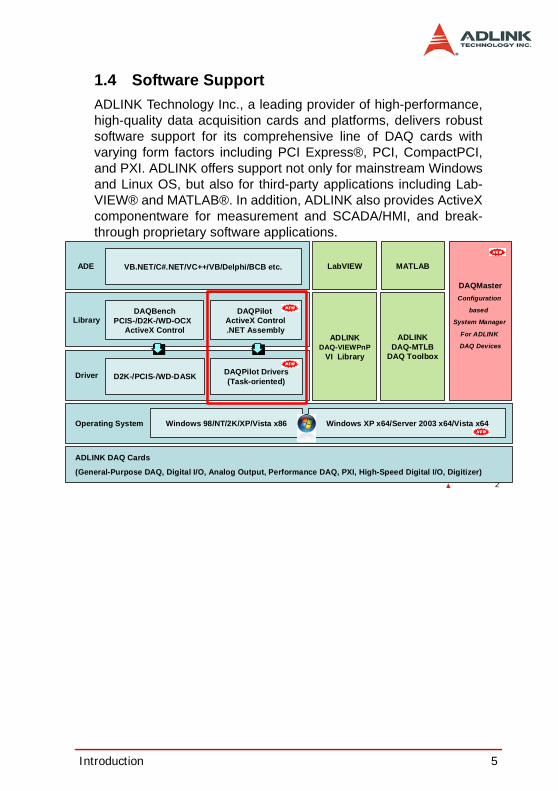
1.4 Software SupportADLINK Technology Inc., a leading provider of high-performance, high-quality data acquisition cards and platforms, delivers robust software support for its comprehensive line of DAQ cards with varying form factors including PCI Express®, PCI, CompactPCI, and PXI. ADLINK offers support not only for mainstream Windows and Linux OS, but also for third-party applications including Lab-VIEW® and MATLAB®. In addition, ADLINK also provides ActiveX componentware for measurement and SCADA/HMI, and break-through proprietary software applications.
Driver
ADE
2
ADLINK DAQ Cards
(General-Purpose DAQ, Digital I/O, Analog Output, Performance DAQ, PXI, High-Speed Digital I/O, Digitizer)
Operating System Windows 98/NT/2K/XP/Vista x86 Windows XP x64/Server 2003 x64/Vista x64
LibraryDAQBench
PCIS-/D2K-/WD-OCX ActiveX Control
DAQPilot ActiveX Control.NET Assembly
VB.NET/C#.NET/VC++/VB/Delphi/BCB etc.
ADLINK DAQ-VIEWPnP
VI Library
D2K-/PCIS-/WD-DASK
LabVIEW MATLAB
ADLINK DAQ-MTLB
DAQ Toolbox
DAQMasterConfiguration
based
System Manager
For ADLINK
DAQ Devices
DAQPilot Drivers (Task-oriented)

6 Introduction
Windows DriversADLINK Task-oriented DAQ Driver/SDK and Wizard for Win-dows
DAQPilot provides one interface for all ADLINK DAQ products via
DAQPilot APIDAQPilot ActiveX ControlDAQPilot .Net Assembly,
DAQPilot (Download and install from the DAQPilot product page: http://www.adlinktech.com/TM/DAQPilot.html
Save development timeShorten learning curve
DAQPilot is a driver and SDK with a graphics-driven interface for various ADE. DAQPilot comes as ADLINK's commitment to pro-vide full support to its comprehensive line of data acquisition prod-ucts. DAQPilot is designed for the beginners as well as experienced programmers. Moreover, because DAQPilot can fin-ish a DAQ task in minutes, it is suitable for programmers aiming to

Introduction 7
immediately program ADLINK DAQ modules and integrate tasks to their own DAQ applications.
Note: ADLINK strongly recommend all users to install the new-generation ADLINK Driver – DAQPilot instead legacy DASK drivers. For those users who have been using the legacy ADLINK DASK Drivers or are not able to connect to the in-ternet, you still can get the latest update from ADLINK all-in-one CD.

8 Introduction
Configuration-Based Device Manager for ADLINK DAQ CardsDAQMaster (.\Utility)
The ADLINK DAQMaster is a smart device manager that enables access to ADLINK data acquisition and test and measurement products. DAQMaster delivers an all-in-one configurations, user can get a full support matrix to well configure ADLINK Test and Measurement products.
DAQMaster enables you to:
Manage ADLINK devices and interfacesManage ADLINK installed softwareManage ADLINK DAQPilot tasks

Introduction 9
ADLINK Legacy DAQ Card Drivers and SDK for WindowsPCIS-DASK (.\Software Package\PCIS-DASK)D2K-DASK (.\Software Package\D2K-DASK)WD-DASK (.\Software Package\WD-DASK)
ADLINK's DASK are advanced 32-bit kernel drivers for custom-ized DAQ application development. DASK enables users to per-form detailed operations and achieve superior performance and reliability from their data acquisition system. DASK kernel drivers now support Windows Vista.
PCIS-DASK for NuDAQ PCI/cPCI SeriesD2K-DASK for DAQ-2000 and PXI-2000 SeriesWD-DASK for High-speed Waveform Digitizer
DASK also supports the following:
Supports Windows Vista 32- or 64-bit editionsSupports AMD64 and Intel x86-64 architecturesDigitally-signed for Windows Vista 64-bit EditionUtilizes WOW64 subsystem to ensure that 32-bit applica-tions run normally on 64-bit Editions of Windows XP, Win-dows 2003 Server, and Windows Vista without modification.
VB.NET
VC++
BCB
Delphi
VB
C#
WD-DASK
D2K-DASK
PCIS-DASK
User Mode
I/O Manager File System
Plug and Pay
Lowest-levelDriver
ConfigurationManager
PowerManager
MemoryManager
ObjectManager
ProcessStructure
ExecutiveSupport
Kernel Mode
Har
dwar
e
DASK Kernel Driver(.sys)
Syst
em S
ervi
ce
Har
dwar
e A
bstr
actio
n La
yer
10 Introduction
More information about Windows Vista Support, please visit http://www.adlinktech.com/TM/VistaSupport.html.
Note: Please use PCIS-DASK with the LPCI-7250 and LPCIe-7250

Introduction 11
Linux DriversLinux Drivers for ADLINK DAQ CardsDrivers are available on the ADLINK website:
PCIS-DASK/XD2K-DASK/XWD-DASK/X
ADLINK's DASK/X drivers are intended for developing customized data acquisition applications under Linux environments. The DASK/X drivers provide common APIs for ADLINK's extensive family of PCI, CompactPCI, and PXI plug-in data acquisition cards, and utilize the full capabilities of these cards under Linux environment.
PCIS-DASK/X for NuDAQ PCI/cPCI Series D2K-DASK/X for DAQ-2000 and PXI-2000 SeriesWD-DASK/X for ADLINK High-speed Waveform Digitizer
More information about Linux drivers, please visit http://www.adlinktech.com/TM/linux_daq.html
Note: Please use PCIS-DASK/X with the LPCI-7250 and LPCIe-7250
12 Introduction
Third-party Software SupportMATLAB® Data Acquisition Toolbox Adapter for ADLINK DAQ Cards
DAQ-MTLB for MATLAB® (.\Software Package\DAQ-MTLB)
The DAQ-MTLB for MATLAB® integrates ADLINK components with MATLAB® Data Acquisition Toolbox and enables users to control a wide range of ADLINK DAQ cards directly from the advanced MATLAB® environment.
Directly control scores of ADLINK DAQ cards that come in different form factors including PCI Express®, PCI, cPCI, and PXICompliant with MATLAB DAQ Toolbox 2.2 or higher (now at R2007a)Critical updates and support are available as ADLINK is now a MathWorks Connections Program partnerADLINK offers the only MATLAB® adapter for high-speed digitizers with up to 65 MHz sampling rate and 14-bit resolu-tion
More information, please visit http://www.adlinktech.com/TM/DAQ-MTLB.html

Introduction 13
LabVIEW™ Data Acquisition VI Set for ADLINK DAQ CardsDAQ Cards DAQ-LVIEW PnP for LabVIEW™ (.\Software Package\DAQ-LVIEW PnP)
The DAQ-LVIEW PnP is a set of LabView Virtual Instruments (Vis) that is fully-compatible with National Instrument's DAQ VIs. Based on the virtual instruments concept, DAQ-LVIEW PnP provides four additional tool panels in LabView, including analog input, analog output, digital I/O, and timer/counter.
The DAQ-LVIEW PnP is designed and verified for LabVIEW 7.0, and is compatible with LabVIEW 6.5, 7.1, 8.0, 8.2 and 8.5.
More information, please visit http://www.adlinktech.com/TM/lab-view-pnp.html

14 Introduction
VEE™ Interface for ADLINK DAQ CardsPCIS-VEE (.\Software Package\PCIS-VEE)D2K-VEE (.\Software Package\D2K-VEE)
Agilent VEE™ is a popular visual programming environment for data acquisition that includes data analysis and control. VEE pro-vides a visual programming interface that allows users to create programs by connecting objects such as acquisition routines, but-tons and displays in a flow diagram. For users that are familiar with Agilent VEE, ADLINK has released the PCIS-VEE and D2K-VEE for seamless integration of the following NuDAQ data acqui-sition cards to the VEE environment:
PCIS-VEE.
VEE for ADLINK NuDAQ Series DAQ cards
6208, 6308, 7200, 7230, 7233, 7234, 7250, 7252, 7248, 7249, 7296, 7300, 7396, 7432, 7433, 7434, 9111, 9112, 9113, 9114, 9118, 9812
D2K-VEE.
VEE for DAQ-2000 Series DAQ cards
2010, 2005, 2006, 2204, 2205, 2206, 2501, 2502
The ADLINK PCIS-VEE and D2K-VEE drivers are designed and verified for Agilent VEE 4.5 environment.

Introduction 15
Componentware/ActiveX Control32-Bit ActiveX Controls for Measurement and SCADA/HMIDAQBench (.\Software Package\DAQBench)
DAQBench is a specialized ActiveX control package designed for 32-bit measurement and SCADA/HMI applications. DAQBench leverages the power of the latest Microsoft ActiveX technology - the standard for code interchangeability and integration under var-ious Windows platform. With DAQBench, programmers can take advantage of their familiarity with development environments such as Visual Basic, Visual C++, Delphi, and Borland C++ Builder to build their own applications.

16 Introduction
Applications for Test and MeasurementSmart & Easy-to-Use Data Acquisition System CreatorDAQCreator (.\Software Package\DAQCreator)
DAQCreator is an out-of-the-box data acquisition software for acquiring, displaying, analyzing, and storing data from ADLINK DAQ cards. Equipped with a smart wizard and intuitive panels, users can easily configure data acquisition settings, change the appearance of data display, perform FFT to acquired data, and store data to a hard disk drive. Another remarkable feature of DAQCreator is the 40 MB/s stream-to-disk data throughput made possible through combination with advanced SCSI technology. DAQCreator delivers a cost-effective solution for high-speed data logging applications.
Get latest ADLINK Software Solutions from ADLINK Web site: http://www.adlinktech.com/TM/software-product.html
Note: All company names appearing herein are trademarks or trade names of their respective owners.
Note: Windows Vista is either a registered trademark or trademark of Microsoft Corporation in the United States and/or other countries.
Installation 17
2 InstallationThis chapter describes how to install and setup the 725X cards. Jumper settings for the digital input channel configurations (AC-fil-ter or Non-AC-filter) and the signal definitions of the 37-pins con-nectors are also specified.
2.1 Unpacking ChecklistCheck the shipping carton for any damage. If the shipping carton and contents are damaged, notify the dealer for a replacement. Retain the shipping carton and packing materials for inspection by the dealer. Obtain authorization before returning any product to ADLINK.
Check the following items are included in the package, if there are any items missing, please contact your dealer:
Included ItemsPCI-7250 (or PCI-7251, cPCI-7252, LPCI-7250, LPCIe-7250) Relay Actuator & Isolated D/I CardADLINK CD (for PCI-7250, cPCI-7252, LPCI-7250, and LPCIe-7250)Software Installation GuideThis User’s Manual
Note: The packaging of OEM versions with non-standard configuration, functionality, or package may vary according to different configuration requests.
CAUTION: The boards must be protected from static discharge and physical shock. Never remove any of the socketed parts except at a static-free workstation. Use the anti-static bag shipped with the product to handle the board. Wear a grounded wrist strap when servicing

18 Installation
2.2 PCB Layout
PCI-7250 PCB Layout
Figure 2-1: PCI-7250 Layout

Installation 19
cPCI-7252 PCB Layout
Figure 2-2: cPCI-7252 Layout
20 Installation
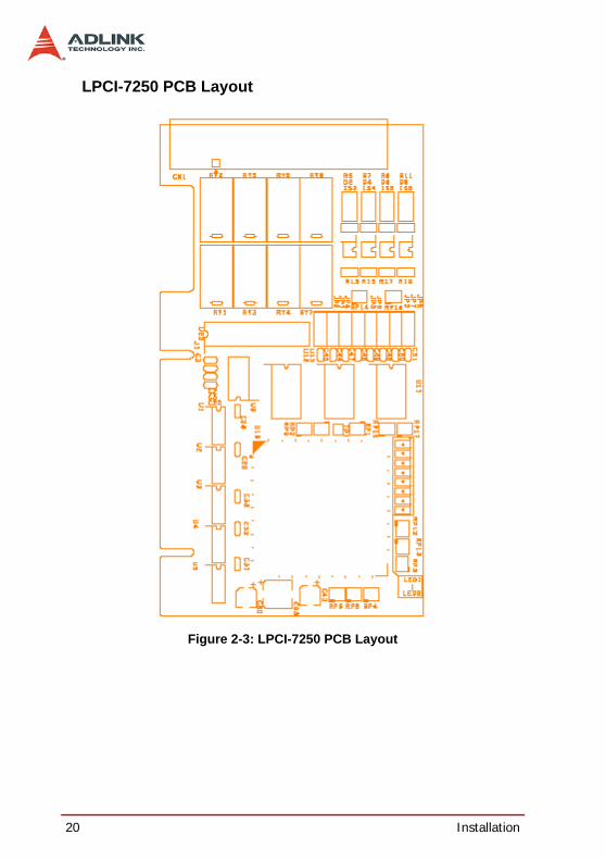
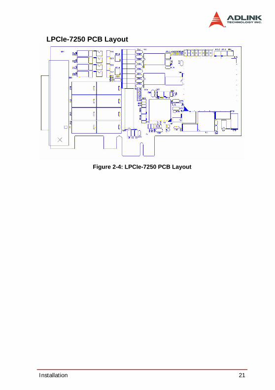
LPCI-7250 PCB Layout
Figure 2-3: LPCI-7250 PCB Layout
Installation 21
LPCIe-7250 PCB Layout
Figure 2-4: LPCIe-7250 PCB Layout

22 Installation
2.3 Input Signal Jumper SettingNote: This section is for PCI-7250, PCI-7251, LPCI-7250, and
LPCIe-7250 only.There are 8 jumpers (JP1 to JP8) on the PCI-7250, PCI-7251, LPCI-7250 and LPCIe-7250; each associated with one digital input to configure that channel as either AC-Filtered or Non-AC-Filtered. Digital input channels and corresponding jumpers are listed in the table below
The default setting for the input signal selection is Non-AC-Filter (DC signal input), which is shown as below:
JP1
JUMPER INPUT SIGNAL
JP1 DI0JP2 DI1JP3 DI2JP4 DI3JP5 DI4JP6 DI5JP7 DI6JP8 DI7
Table 2-1: Jumpers and DI Channels
Input Signal Selection Non-AC-Filter(DC Signal)
AC-Filter(AC Signal)
Jumper JP1 - JP8 2-3 1-2
Table 2-2: Input Signal Selection Jumper Settings

Installation 23
2.4 Hardware Installation Outline
PCI ConfigurationPCI cards (or CompactPCI cards) are equipped with plug and play PCI controllers which can request base addresses and interrupts according to the PCI standard. The system BIOS will assign the system resources based on the PCI card configuration registers and system parameters (which are set by the system BIOS). Inter-rupt assignment and memory usage (I/O port locations) can only be assigned by the system BIOS. These system resource assign-ments are done on a board-by-board basis. It is not suggested to assign the system resource by any other methods.
PCI Slot SelectionThe PCI card can be inserted into any PCI slot without any config-uration of the system resources. The CompactPCI card can also be inserted into any CompactPCI I/O slot.
Installation Procedures1. Turn off your computer
2. Turn off all accessories (printer, modem, monitor, etc.) connected to your computer.
3. Remove the cover from your computer.
4. Setup jumpers on the PCI or CompactPCI card.
5. Select a 32-bit PCI slot. PCI slot are shorter than ISA or EISA slots, and are usually white or ivory.
6. Before handling the PCI cards, discharge any static buildup on your body by touching the metal case of the computer. Hold the edge and do not touch the compo-nents.
7. Position the board into the PCI slot you selected.
8. Secure the card in place at the rear panel of the system.
24 Installation
2.5 Device Installation for Windows SystemsOnce Windows Vista/XP/2003/2000 has started, the Plug and Play functions of the Windows system will find and locate the new NuDAQ/NuIPC card. If this is the first time a NuDAQ/NuIPC card is installed in your Windows system, you will be prompted to input the device information source. Please refer to the “Software Instal-lation Guide” for installation procedures for the device drivers.
2.6 Connector Pin Assignments
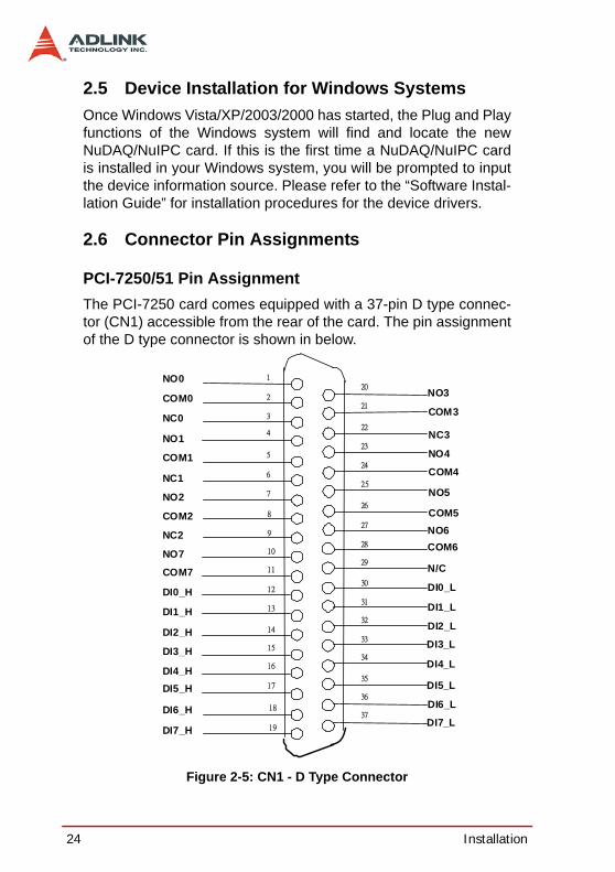
PCI-7250/51 Pin AssignmentThe PCI-7250 card comes equipped with a 37-pin D type connec-tor (CN1) accessible from the rear of the card. The pin assignment of the D type connector is shown in below.
Figure 2-5: CN1 - D Type Connector
1
2
3
4
5
6
10
11
12
13
14
15
7
8
9
16
17
18
19
20
21
22
23
24
25
26
27
28
30
31
32
33
29
35
36
37
34
COM0
NC0
NO1
COM1
NC1
NO2
COM2
NC2
COM7DI0
DI1
DI2
DI3
DI4
DI5
NO7
DI6
DI7
NO3
COM3
NC3
NO4
COM4
NO5
COM5NO6COM6
N/C
NO0
DI0
DI1
DI2
DI3
DI4DI5
DI6
DI7
1
2
3
4
5
6
10
11
12
13
14
15
7
8
9
16
17
18
19
20
21
22
23
24
25
26
27
28
30
31
32
33
29
35
36
37
34
COM0
NC0
NO1
COM1
NC1
NO2
COM2
NC2
COM7DI0_L
DI1_L
DI2_L
DI3_L
DI4_L
DI5_L
NO7
DI6_L
DI7_L
NO3
COM3
NC3
NO4
COM4
NO5
COM5NO6COM6
N/C
NO0
DI0_H
DI1_H
DI2_H
DI3_H
DI4_HDI5_H
DI6_H
DI7_H
Installation 25
Legend
Din: Digital input low, channel n (input signal Is not polarity sensitive)
NC n: Normal close pin of relay nNO n: Normal open pin of relay n
COM n: Common pin of relay nN/C: No connection
Table 2-3: CN1 - PCI-7250/51 Pin Assignment

26 Installation
cPCI-7252 Pin Assignment
Signal Pin Pin Signal
IGND 1 26 IGND
DI8 2 27 DI12
DI9 3 28 DI13
DI10 4 29 DI14
DI11 5 30 DI15
DI0L 6 31 DI4H
DI0H 7 32 DI4L
DI1L 8 33 DI5H
DI1H 9 34 DI5L
D2IL 10 35 DI6H
DI2H 11 36 DI6L
DI3L 12 37 DI7H
DI3H 13 38 DI7L
NO0 14 39 NO5
NO1 15 40 NO4
COM0 16 41 COM5
COM1 17 42 COM4
NC0 18 43 NC5
NC1 19 44 NC4
NO2 20 45 NO7
NO3 21 46 NO6
COM2 22 47 COM7
COM3 23 48 COM6
NC2 24 49 NC7
NC3 25 50 NC6
Table 2-4: CN1 - cPCI-7252 Pin Assignment
LegendDin: Digital input channel n
IGND: Ground of DIn signalsDinH: Digital input channel n with positive polarityDinL: Digital input channel n with negative polarityNC n: Normal close pin of relay nNO n: Normal open pin of relay n
COM n: Common pin of relay n

Installation 27
LPCI/LPCIe-7250 CN1 Pin Assignment
Signal Pin Pin Signal
NO0 1 26 NO4
COM0 2 27 COM4
NC0 3 28 NC4
NO1 4 29 NO5
COM1 5 30 COM5
NC1 6 31 NC5
NO2 7 32 NO6
COM2 8 33 COM6
NC2 9 34 NC6
NO3 10 35 NO7
COM3 11 36 COM7
NC3 12 37 NC7
N/C 13 38 N/C
N/C 14 39 N/C
N/C 15 40 N/C
N/C 16 41 N/C
N/C 17 42 N/C
IDI_0H 18 43 IDI_0L
IDI_1H 19 44 IDI_1L
IDI_2H 20 45 IDI_2L
IDI_3H 21 46 IDI_3L
IDI_4H 22 47 IDI_4L
IDI_5H 23 48 IDI_5L
IDI_6H 24 49 IDI_6L
IDI_7H 25 50 IDI_7L
Table 2-5: LPCI/LPCIe-7250 CN1 Pin Assignment
LegendDin: Digital input channel n
IGND: Ground of DIn signalsDinH: Digital input channel n with positive polarityDinL: Digital input channel n with negative polarityNC n: Normal close pin of relay nNO n: Normal open pin of relay n
COM n: Common pin of relay n

28 Installation
2.7 PCI-7250 and PCI-7251 ConnectionThere are 8-relay outputs and 8-isolation inputs on both the PCI-7250 and PCI-7251. The PCI-7251 is used as an expansion for the PCI-7250. The operations of the PCI-7251 are the same as that of the PCI-7250. There can be at most 3 PCI-7251 expansion boards to one PCI-7250. Therefore, the PCI-7250 can control up to 32 relays and detect 32 input signals.
Figure 2-6: Connection between PCI-7250 and PCI-7251

Registers 29
3 RegistersDetailed descriptions of the registers are specified in this chapter. This information is useful for programmers who wish to control the card with low-level programming. However, we suggest users fully understand the PCI interface before starting any low-level pro-gramming. In addition, the contents of this chapter will also help users understand how to use the software drivers to configure this card.
3.1 PCI PnP Registers This PCI card functions as a 32-bit PCI target device to any mas-ter on the PCI bus. There are three types of registers: PCI Config-uration Registers (PCR), Local Configuration Registers (LCR) and 725X registers.
The PCR, which is PCI-bus specification compliant, is initialized and controlled by the Plug and Play (PnP) PCI BIOS. Users may obtain more information on the PCI BIOS specification to better understand the operation of the PCR. Please contact PCISIG to acquire PCI interface specifications.
The PCI bus controller PCI-9050 is provided by PLX Technology Inc. (www.plxtech.com). For more information about the LCR, please visit PLX Technology’s web site to download relative infor-mation. It is not necessary for users to fully understand the details of the LCR if the software library provided is used. The PCI PnP BIOS assigns the base address of the LCR. The assigned address is located at an offset of 14h from the PCR.
The 725X registers are discussed in the next section. The base address, which is also assigned by the PCI PnP BIOS, is located at an offset of 18h from the PCR. Therefore, users can read the address 18h from the PCR to obtain its base address by using the BIOS function call. Do not attempt to modify the base address and interrupt that have been assigned by the PCI PnP BIOS, it may cause resource conflicts with your system.

30 Registers
3.2 I/O Address MapAll 725X registers are 8 bits long. Users can access these regis-ters using 8-bit I/O instructions. Using these registers will allow the relays and status of the inputs to be controlled. The following table shows the registers address map, including descriptions and their offset addresses relative to the base address. If the PCI-7251 expansion boards are not installed, corresponding registers have no significance.
3.3 Relay Output and Readback RegistersThere are 8 relays on each PCI-7250/7251, LPCI-7250, LPCIe-7250, and cPCI-7252 board. Each relay is controlled by one bit in the control register. Bit value ‘0’ means the relay is not energized.
Offset Write Read Board
0 Relay Output Output readbackPCI-7250
1 Not used Isolation Input2 Relay Output Output readback
PCI-7251 #13 Not used Isolation Input4 Relay Output Output readback
PCI-7251 #25 Not used Isolation Input6 Relay Output Output readback
PCI-7251 #37 Not used Isolation Input
Table 3-1: PCI-7250 Address Map with PCI-7251 Installed
Offset Write Read Board
0 Relay Output Isolation InputcPCI-72521 Not used Not used
2 Not used Output readback
Table 3-2: cPCI-7252 Address Map
Offset Write Read Board
0 Relay Output Output readback LPCI-7250/LPCIe-72501 Not used Isolation Input
Table 3-3: LPCI/LPCIe-7250 Address Map

Registers 31
The normal open signal line is ‘open’. Bit value ‘1’ means the relay is energized and the normal open signal line is now closed.
The initial bit values of the control register are all ‘0’ and the status of the relay can be readback from the readback register. If the relay is open, the corresponding bit value read is ‘0’. If the relay is closed, the bit value read is ‘1’.
3.4 Isolation Input RegistersThere are 8 isolated input channels on the PCI-7250 / 7251 board. The status of the 8 channels can be read from the isolation input register. Each bit corresponds to each channel. Bit value “1” means input voltage is high and “0” means input voltage is low.
Note: Bits 8-15 are for cPCI-7252 only
Bit 7 6 5 4 3 2 1 0
Relay Output DO7 DO6 DO5 DO4 DO3 DO2 DO1 DO0Output Readback RB7 RB6 RB5 RB4 RB3 RB2 RB1 RB0
Table 3-4: Data Format of Relay Output and Readback Status Registers
Bit 7 6 5 4 3 2 1 0Iso. Input DI7 DI6 DI5 DI4 DI3 DI2 DI1 DI0
Bit 15 14 13 12 11 10 9 8Iso. Input DI15 DI14 DI13 DI12 DI11 DI10 DI9 DI8
Table 3-5: Relay Output

32 Registers

Operation Theory 33
4 Operation Theory4.1 Using Relay OutputThe PCI-7250/7251 contains two types of relays: Form C and Form A. Relays R0 - R3 are form C relays, and R4 - R7 are plain form A type. Note that the LPCI-7250, LPCIe-7250, and cPCI-7252 contain Form C relays only. The differences between these two types of relays are:
1. Form C Relay: (R0 - R3)
Figure 4-1: Form C Relay
Form C type relays have three contacts: NC (Normal Close), NO (Normal Open), and COM (Common). The COM post, located at the middle, must make contact with either the NO post or NC post. When the control bit is high (1), there is contact between the COM post and NO post. If the control bit is low (0), there is contact between the COM post and NC post.
In normal power-up and reset, the relay is in low status.
NO
NCCOM
Control Bit = High (1)
NO
NCCOM
Control Bit = Low (0)

34 Operation Theory
2. Form A Relay: (R4 - R7)
Figure 4-2: Form A Relay
Form A relay only has two contacts: NO (Normal Open) and COM (Common). The COM post can make contact either with the NO post or not. When the control bit is high (1), the COM post and NO post are contacted. If the control bit is low (0), the COM post and NO post does not make contact.
In normal power-up and reset, the relay is in low status.
The relay output contacts are rated at a maximum of 0.5 at 120 VAC (resistive), 1 A 24 VDC, or 0.3 A 60 VDC. You should reduce these ratings for inductive loads. For more information on relay contact, please refer to the Appendix.
NO
Control Bit = High(1)
COM
NO
Control Bit = Low(0)
COM

Operation Theory 35
4.2 Using Isolated InputThe PCI-7250 (or PCI-7251) contains 8 identical opto-isolated control input channels. The circuit diagram of the differential input channel is shown below.
Figure 4-3: PCI-7250 Differential Input Circuit
The digital input is first routed through a photo-coupler (PC-814), which is shown in the following diagram.
The cPCI-7252 contains 16 identical opto-isolated control input channels. The circuit diagram of the differential input signals of channel number 0-7 are the same as of the PCI-7250. While the input signals for channel numbers 8-15 are isolated inputs, the connection is not polarity sensitive whether AC or DC voltage is used.
Figure 4-4: cPCI-7252 Isolated Input Circuit
V IN
2.2k Ω
Ri
PC-814 (opto-isolator)
I F
DInH
DInL
V IN
1.2k Ω
Ri
PC-814 (opto-isolator)
I F
DInH
IGND
36 Operation Theory
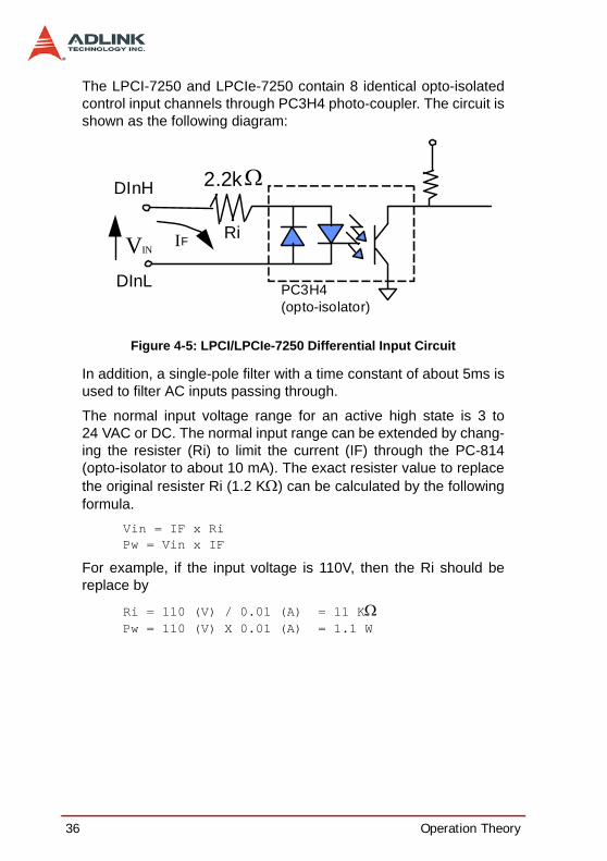
The LPCI-7250 and LPCIe-7250 contain 8 identical opto-isolated control input channels through PC3H4 photo-coupler. The circuit is shown as the following diagram:
Figure 4-5: LPCI/LPCIe-7250 Differential Input Circuit
In addition, a single-pole filter with a time constant of about 5ms is used to filter AC inputs passing through.
The normal input voltage range for an active high state is 3 to 24 VAC or DC. The normal input range can be extended by chang-ing the resister (Ri) to limit the current (IF) through the PC-814 (opto-isolator to about 10 mA). The exact resister value to replace the original resister Ri (1.2 KΩ) can be calculated by the following formula.
Vin = IF x RiPw = Vin x IF
For example, if the input voltage is 110V, then the Ri should be replace by
Ri = 110 (V) / 0.01 (A) = 11 KΩPw = 110 (V) X 0.01 (A) = 1.1 W
V IN
2.2k Ω
Ri
PC3H4 (opto-isolator)
I F
DInH
DInL

Appendix 37
Appendix
Relay Contact Protection CircuitsThe contacts are the most important elements of a relay construc-tion, Contact performance conspicuously influenced by contact material, and voltage and current values applied to the contacts.
Another important issue is contact protection; the right contact pro-tection circuit can suppress the counter EMF to a low level. How-ever, note that incorrect use will result in an adverse effect. Typical contact protection circuits are given below:
RC Circuit This circuit is suitable for DC applications. If the load is a timer, leakage current flow through the RC circuit may cause faulty oper-ation.
The circuit below is suitable for both DC and AC applications. If the load is a relay or solenoid, the release time is lengthened. Effective when connected to both contacts if the power supply volt-age is 24V or 48V and the voltage cross the load is 100 to 200V.
Contact
InductiveLoadR C
Contact
InductiveLoad
RC

38 Appendix
Device Selection:As a guide in selecting R and C,
R: 0.5 to 1Ω per 1V contact voltageC: 0.5 to 1μF per 1A contact current
Values vary depending on the properties of the capacitor C acting to suppress the discharge the moment the contacts open. Resistor R acts to limit the current when the power is turned on. Test to confirm. Use a capacitor with a breakdown voltage of 200 to 300V. Use AC type capacitors (non-polarized) for AC circuits.
Diode CircuitThis circuit is suitable for DC applications. The diode connected in parallel causes the energy stored in the coil to flow to the coil in the form of current and dissipates it as joule heat at the resistive component of the inductive load. This circuit further delays the release time compared to the RC circuit.
Device Selection:Use a diode with a reverse breakdown voltage of at least 10 times the circuit voltage and a forward current at least as large as the load current.
Contact
InductiveLoad
Diode

Appendix 39
Diode & Zener diode Circuit This circuit is also suitable for DC application. Effective when the release time i in the diode circuit is too long.
Device Selection:Use a zener diode with a zener voltage about the same as the power supply voltage.
Varistor Circuit This circuit is also suitable for both AC & DC applications. Using the stable voltage characteristics of the varistor, this circuit pre-vents excessively high voltages from being applied across the contacts. This circuit also slightly delays the release time. Effective when connected to both contacts if the power supply voltage is 24V or 48V and the voltage cross the load is 100 to 200V.
Contact
InductiveLoad
Diode
Contact
InductiveLoad
Diode

40 Appendix