pc16550d universal asynchronous receiver/transmitter with ... · pdf filepc16550d universal...
TRANSCRIPT
TL/C/8652
PC
16550D
Univ
ers
alA
synchro
nous
Receiv
er/
Tra
nsm
itterw
ithFIF
Os
June 1995
PC16550D Universal AsynchronousReceiver/Transmitter with FIFOs²
General DescriptionThe PC16550D is an improved version of the original 16450
Universal Asynchronous Receiver/Transmitter (UART).
Functionally identical to the 16450 on powerup (CHARAC-
TER mode)* the PC16550D can be put into an alternate
mode (FIFO mode) to relieve the CPU of excessive software
overhead.
In this mode internal FIFOs are activated allowing 16 bytes
(plus 3 bits of error data per byte in the RCVR FIFO) to be
stored in both receive and transmit modes. All the logic is on
chip to minimize system overhead and maximize system ef-
ficiency. Two pin functions have been changed to allow sig-
nalling of DMA transfers.
The UART performs serial-to-parallel conversion on data
characters received from a peripheral device or a MODEM,
and parallel-to-serial conversion on data characters re-
ceived from the CPU. The CPU can read the complete
status of the UART at any time during the functional opera-
tion. Status information reported includes the type and con-
dition of the transfer operations being performed by the
UART, as well as any error conditions (parity, overrun, fram-
ing, or break interrupt).
The UART includes a programmable baud rate generator
that is capable of dividing the timing reference clock input
by divisors of 1 to (216b1), and producing a 16 c clock for
driving the internal transmitter logic. Provisions are also in-
cluded to use this 16 c clock to drive the receiver logic. The
UART has complete MODEM-control capability, and a proc-
essor-interrupt system. Interrupts can be programmed to
the user’s requirements, minimizing the computing required
to handle the communications link.
The UART is fabricated using National Semiconductor’s ad-
vanced M2CMOS process.
*Can also be reset to 16450 Mode under software control.
²Note: This part is patented.
FeaturesY Capable of running all existing 16450 software.Y Pin for pin compatible with the existing 16450 except
for CSOUT (24) and NC (29). The former CSOUT and
NC pins are TXRDY and RXRDY, respectively.Y After reset, all registers are identical to the 16450 reg-
ister set.Y In the FIFO mode transmitter and receiver are each
buffered with 16 byte FIFO’s to reduce the number of
interrrupts presented to the CPU.Y Adds or deletes standard asynchronous communication
bits (start, stop, and parity) to or from the serial data.Y Holding and shift registers in the 16450 Mode eliminate
the need for precise synchronization between the CPU
and serial data.Y Independently controlled transmit, receive, line status,
and data set interrupts.Y Programmable baud generator divides any input clock
by 1 to (216 b 1) and generates the 16 c clock.Y Independent receiver clock input.Y MODEM control functions (CTS, RTS, DSR, DTR, RI,
and DCD).Y Fully programmable serial-interface characteristics:
Ð 5-, 6-, 7-, or 8-bit characters
Ð Even, odd, or no-parity bit generation and detection
Ð 1-, 1(/2-, or 2-stop bit generation
Ð Baud generation (DC to 1.5M baud).Y False start bit detection.Y Complete status reporting capabilities.Y TRI-STATEÉ TTL drive for the data and control buses.Y Line break generation and detection.Y Internal diagnostic capabilities:
Ð Loopback controls for communications link fault
isolation
Ð Break, parity, overrun, framing error simulation.Y Full prioritized interrupt system controls.
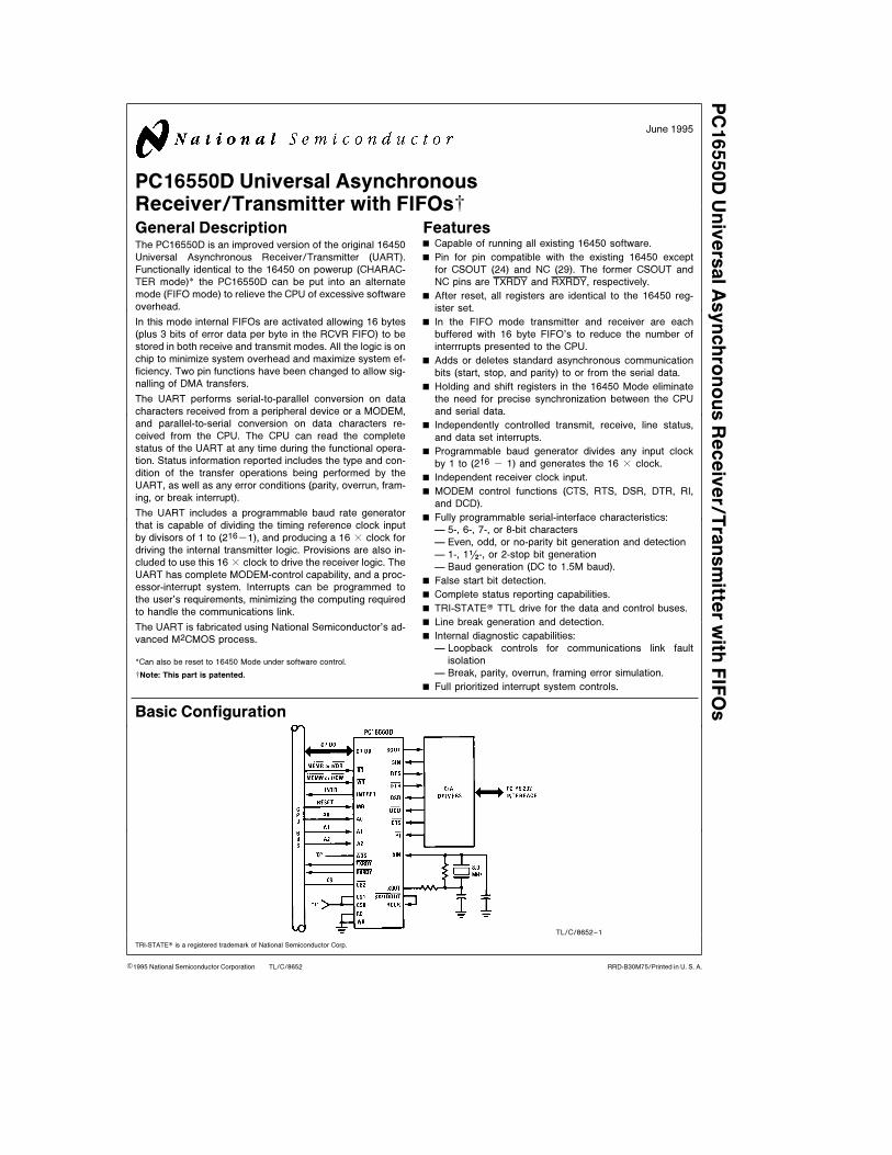
Basic Configuration
TL/C/8652–1
TRI-STATEÉ is a registered trademark of National Semiconductor Corp.
C1995 National Semiconductor Corporation RRD-B30M75/Printed in U. S. A.
Table of Contents
1.0 ABSOLUTE MAXIMUM RATINGS
2.0 DC ELECTRICAL CHARACTERISTICS
3.0 AC ELECTRICAL CHARACTERISTICS
4.0 TIMING WAVEFORMS
5.0 BLOCK DIAGRAM
6.0 PIN DESCRIPTIONS
7.0 CONNECTION DIAGRAMS
8.0 REGISTERS
8.1 Line Control Register
8.2 Typical Clock Circuits
8.0 REGISTERS (Continued)
8.3 Programmable Baud Generator
8.4 Line Status Register
8.5 FIFO Control Register
8.6 Interrupt Identification Register
8.7 Interrupt Enable Register
8.8 Modem Control Register
8.9 Modem Status Register
8.10 Scratchpad Register
8.11 FIFO Interrupt Mode Operation
8.12 FIFO Polled Mode Operation
9.0 TYPICAL APPLICATIONS
2
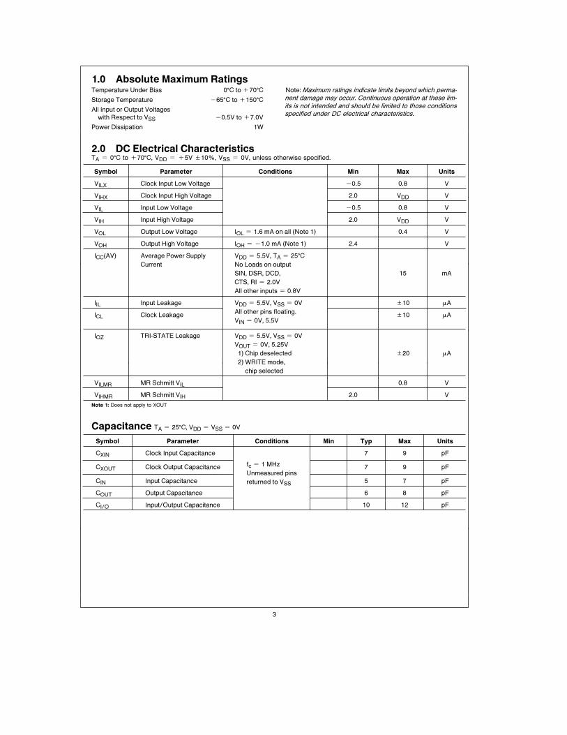
1.0 Absolute Maximum RatingsTemperature Under Bias 0§C to a70§CStorage Temperature b65§C to a150§CAll Input or Output Voltages
with Respect to VSS b0.5V to a7.0V
Power Dissipation 1W
Note: Maximum ratings indicate limits beyond which perma-nent damage may occur. Continuous operation at these lim-its is not intended and should be limited to those conditionsspecified under DC electrical characteristics.
2.0 DC Electrical CharacteristicsTA e 0§C to a70§C, VDD e a5V g10%, VSS e 0V, unless otherwise specified.
Symbol Parameter Conditions Min Max Units
VILX Clock Input Low Voltage b0.5 0.8 V
VIHX Clock Input High Voltage 2.0 VDD V
VIL Input Low Voltage b0.5 0.8 V
VIH Input High Voltage 2.0 VDD V
VOL Output Low Voltage IOL e 1.6 mA on all (Note 1) 0.4 V
VOH Output High Voltage IOH e b1.0 mA (Note 1) 2.4 V
ICC(AV) Average Power Supply VDD e 5.5V, TA e 25§CCurrent No Loads on output
SIN, DSR, DCD, 15 mA
CTS, RI e 2.0V
All other inputs e 0.8V
IIL Input Leakage VDD e 5.5V, VSS e 0V g10 mA
ICL Clock LeakageAll other pins floating.
g10 mAVIN e 0V, 5.5V
IOZ TRI-STATE Leakage VDD e 5.5V, VSS e 0V
VOUT e 0V, 5.25V
1) Chip deselected g20 mA
2) WRITE mode,
chip selected
VILMR MR Schmitt VIL 0.8 V
VIHMR MR Schmitt VIH 2.0 V
Note 1: Does not apply to XOUT
Capacitance TA e 25§C, VDD e VSS e 0V
Symbol Parameter Conditions Min Typ Max Units
CXIN Clock Input Capacitance 7 9 pF
fc e 1 MHzCXOUT Clock Output Capacitance 7 9 pFUnmeasured pins
CIN Input Capacitance 5 7 pFreturned to VSS
COUT Output Capacitance 6 8 pF
CI/O Input/Output Capacitance 10 12 pF
3
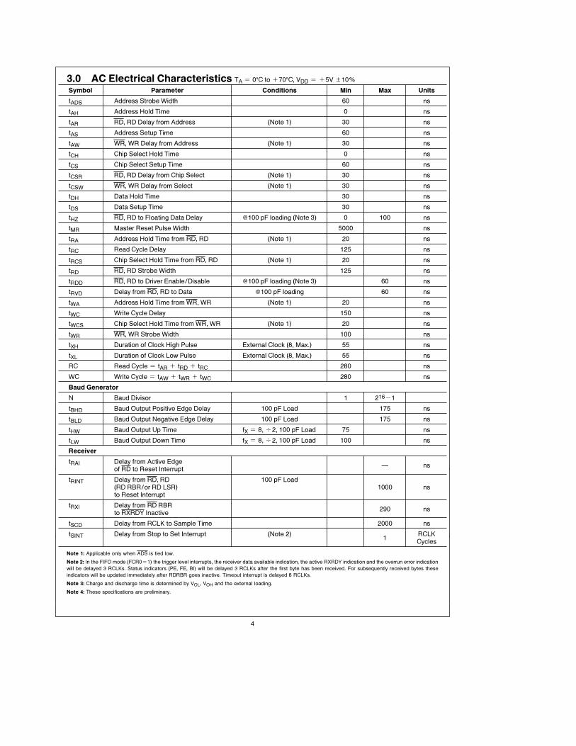
3.0 AC Electrical Characteristics TA e 0§C to a70§C, VDD e a5V g10%
Symbol Parameter Conditions Min Max Units
tADS Address Strobe Width 60 ns
tAH Address Hold Time 0 ns
tAR RD, RD Delay from Address (Note 1) 30 ns
tAS Address Setup Time 60 ns
tAW WR, WR Delay from Address (Note 1) 30 ns
tCH Chip Select Hold Time 0 ns
tCS Chip Select Setup Time 60 ns
tCSR RD, RD Delay from Chip Select (Note 1) 30 ns
tCSW WR, WR Delay from Select (Note 1) 30 ns
tDH Data Hold Time 30 ns
tDS Data Setup Time 30 ns
tHZ RD, RD to Floating Data Delay @100 pF loading (Note 3) 0 100 ns
tMR Master Reset Pulse Width 5000 ns
tRA Address Hold Time from RD, RD (Note 1) 20 ns
tRC Read Cycle Delay 125 ns
tRCS Chip Select Hold Time from RD, RD (Note 1) 20 ns
tRD RD, RD Strobe Width 125 ns
tRDD RD, RD to Driver Enable/Disable @100 pF loading (Note 3) 60 ns
tRVD Delay from RD, RD to Data @100 pF loading 60 ns
tWA Address Hold Time from WR, WR (Note 1) 20 ns
tWC Write Cycle Delay 150 ns
tWCS Chip Select Hold Time from WR, WR (Note 1) 20 ns
tWR WR, WR Strobe Width 100 ns
tXH Duration of Clock High Pulse External Clock (8, Max.) 55 ns
tXL Duration of Clock Low Pulse External Clock (8, Max.) 55 ns
RC Read Cycle e tAR a tRD a tRC 280 ns
WC Write Cycle e tAW a tWR a tWC 280 ns
Baud Generator
N Baud Divisor 1 216b1
tBHD Baud Output Positive Edge Delay 100 pF Load 175 ns
tBLD Baud Output Negative Edge Delay 100 pF Load 175 ns
tHW Baud Output Up Time fX e 8, d2, 100 pF Load 75 ns
tLW Baud Output Down Time fX e 8, d2, 100 pF Load 100 ns
Receiver
tRAI Delay from Active EdgeÐ ns
of RD to Reset Interrupt
tRINT Delay from RD, RD 100 pF Load(RD RBR/or RD LSR) 1000 nsto Reset Interrupt
tRXI Delay from RD RBR290 ns
to RXRDY Inactive
tSCD Delay from RCLK to Sample Time 2000 ns
tSINT Delay from Stop to Set Interrupt (Note 2)1
RCLKCycles
Note 1: Applicable only when ADS is tied low.
Note 2: In the FIFO mode (FCR0e1) the trigger level interrupts, the receiver data available indication, the active RXRDY indication and the overrun error indication
will be delayed 3 RCLKs. Status indicators (PE, FE, BI) will be delayed 3 RCLKs after the first byte has been received. For subsequently received bytes these
indicators will be updated immediately after RDRBR goes inactive. Timeout interrupt is delayed 8 RCLKs.
Note 3: Charge and discharge time is determined by VOL, VOH and the external loading.
Note 4: These specifications are preliminary.
4
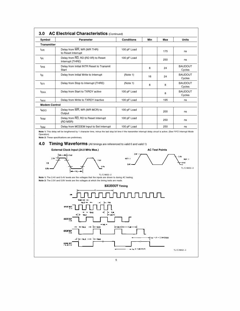
3.0 AC Electrical Characteristics (Continued)
Symbol Parameter Conditions Min Max Units
Transmitter
tHR Delay from WR, WR (WR THR) 100 pF Load175 ns
to Reset Interrupt
tIR Delay from RD, RD (RD IIR) to Reset 100 pF Load250 ns
Interrupt (THRE)
tIRS Delay from Initial INTR Reset to Transmit8 24
BAUDOUT
Start Cycles
tSI Delay from Initial Write to Interrupt (Note 1)16 24
BAUDOUT
Cycles
tSTI Delay from Stop to Interrupt (THRE) (Note 1)8 8
BAUDOUT
Cycles
tSXA Delay from Start to TXRDY active 100 pF Load8
BAUDOUT
Cycles
tWXI Delay from Write to TXRDY inactive 100 pF Load 195 ns
Modem Control
tMDO Delay from WR, WR (WR MCR) to 100 pF Load200 ns
Output
tRIM Delay from RD, RD to Reset Interrupt 100 pF Load250 ns
(RD MSR)
tSIM Delay from MODEM Input to Set Interrupt 100 pF Load 250 ns
Note 1: This delay will be lengthened by 1 character time, minus the last stop bit time if the transmitter interrupt delay circuit is active. (See FIFO Interrupt Mode
Operation).
Note 2: These specifications are preliminary.
4.0 Timing Waveforms (All timings are referenced to valid 0 and valid 1)
External Clock Input (24.0 MHz Max.)
TL/C/8652–2
AC Test Points
TL/C/8652–3
Note 1: The 2.4V and 0.4V levels are the voltages that the inputs are driven to during AC testing.
Note 2: The 2.0V and 0.8V levels are the voltages at which the timing tests are made.
BAUDOUT Timing
TL/C/8652–4
5
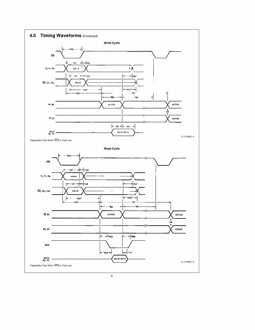
4.0 Timing Waveforms (Continued)
Write Cycle
TL/C/8652–5
*Applicable Only When ADS is Tied Low.
Read Cycle
TL/C/8652–6
*Applicable Only When ADS is Tied Low.
6
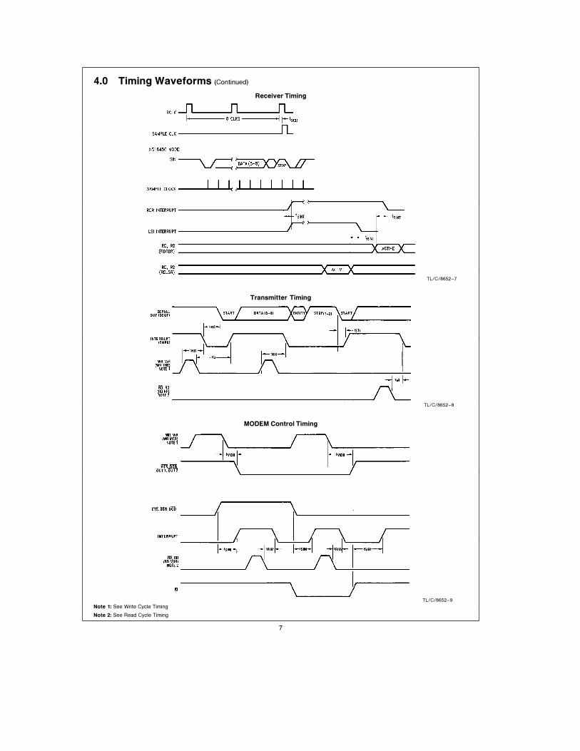
4.0 Timing Waveforms (Continued)
Receiver Timing
TL/C/8652–7
Transmitter Timing
TL/C/8652–8
MODEM Control Timing
TL/C/8652–9
Note 1: See Write Cycle Timing
Note 2: See Read Cycle Timing
7
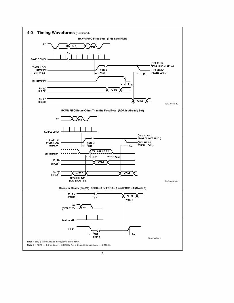
4.0 Timing Waveforms (Continued)
RCVR FIFO First Byte (This Sets RDR)
TL/C/8652–10
RCVR FIFO Bytes Other Than the First Byte (RDR Is Already Set)
TL/C/8652–11
Receiver Ready (Pin 29) FCR0e0 or FCR0e1 and FCR3e0 (Mode 0)
TL/C/8652–12
Note 1: This is the reading of the last byte in the FIFO.
Note 2: If FCR0 e 1, then tSINT e 3 RCLKs. For a timeout interrupt, tSINT e 8 RCLKs.
8
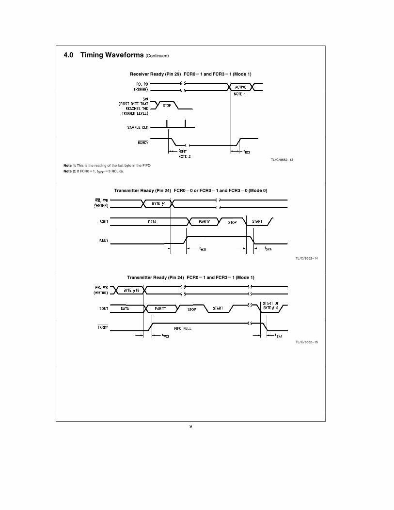
4.0 Timing Waveforms (Continued)
Receiver Ready (Pin 29) FCR0e1 and FCR3e1 (Mode 1)
TL/C/8652–13
Note 1: This is the reading of the last byte in the FIFO.
Note 2: If FCR0e1, tSINTe3 RCLKs.
Transmitter Ready (Pin 24) FCR0e0 or FCR0e1 and FCR3e0 (Mode 0)
TL/C/8652–14
Transmitter Ready (Pin 24) FCR0e1 and FCR3e1 (Mode 1)
TL/C/8652–15
9
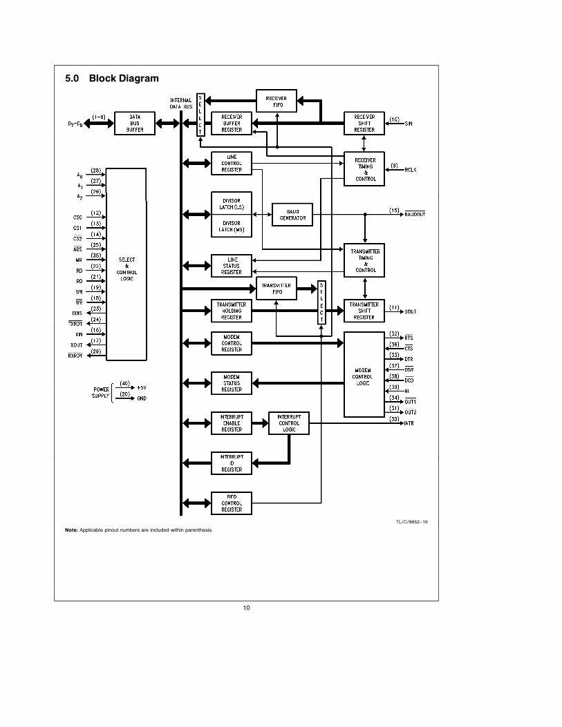
5.0 Block Diagram
TL/C/8652–16
Note: Applicable pinout numbers are included within parenthesis.
10

6.0 Pin DescriptionsThe following describes the function of all UART pins. Some
of these descriptions reference internal circuits.
In the following descriptions, a low represents a logic 0 (0V
nominal) and a high represents a logic 1 (a2.4V nominal).
A0, A1, A2, Register Select, Pins 26–28: Address signals
connected to these 3 inputs select a UART register for the
CPU to read from or write to during data transfer. A table of
registers and their addresses is shown below. Note that the
state of the Divisor Latch Access Bit (DLAB), which is the
most significant bit of the Line Control Register, affects the
selection of certain UART registers. The DLAB must be set
high by the system software to access the Baud Generator
Divisor Latches.
Register Addresses
DLAB A2 A1 A0 Register
0 0 0 0 Receiver Buffer (read),
Transmitter Holding
Register (write)
0 0 0 1 Interrupt Enable
X 0 1 0 Interrupt Identification (read)
X 0 1 0 FIFO Control (write)
X 0 1 1 Line Control
X 1 0 0 MODEM Control
X 1 0 1 Line Status
X 1 1 0 MODEM Status
X 1 1 1 Scratch
1 0 0 0 Divisor Latch
(least significant byte)
1 0 0 1 Divisor Latch
(most significant byte)
ADS, Address Strobe, Pin 25: The positive edge of an active
Address Strobe (ADS) signal latches the Register Select
(A0, A1, A2) and Chip Select (CS0, CS1, CS2) signals.
Note: An active ADS input is required when the Register Select (A0, A1, A2)
and Chip Select (CS0, CS1, CS2) signals are not stable for the dura-
tion of a read or write operation. If not required, tie the ADS input
permanently low.
BAUDOUT, Baud Out, Pin 15: This is the 16 c clock signal
from the transmitter section of the UART. The clock rate is
equal to the main reference oscillator frequency divided by
the specified divisor in the Baud Generator Divisor Latches.
The BAUDOUT may also be used for the receiver section by
tying this output to the RCLK input of the chip.
CS0, CS1, CS2, Chip Select, Pins 12–14: When CS0 and
CS1 are high and CS2 is low, the chip is selected. This
enables communication between the UART and the CPU.
The positive edge of an active Address Strobe signal latch-
es the decoded chip select signals, completing chip selec-
tion. If ADS is always low, valid chip selects should stabilize
according to the tCSW parameter.
CTS, Clear to Send, Pin 36: When low, this indicates that
the MODEM or data set is ready to exchange data. The CTS
signal is a MODEM status input whose conditions can be
tested by the CPU reading bit 4 (CTS) of the MODEM Status
Register. Bit 4 is the complement of the CTS signal. Bit 0
(DCTS) of the MODEM Status Register indicates whether
the CTS input has changed state since the previous reading
of the MODEM Status Register. CTS has no effect on the
Transmitter.
Note: Whenever the CTS bit of the MODEM Status Register changes state,
an interrupt is generated if the MODEM Status Interrupt is enabled.
D7–D0, Data Bus, Pins 1–8: This bus comprises eight TRI-
STATE input/output lines. The bus provides bidirectional
communications between the UART and the CPU. Data,
control words, and status information are transferred via the
D7–D0 Data Bus.
DCD, Data Carrier Detect, Pin 38: When low, indicates that
the data carrier has been detected by the MODEM or data
set. The DCD signal is a MODEM status input whose condi-
tion can be tested by the CPU reading bit 7 (DCD) of the
MODEM Status Register. Bit 7 is the complement of the
DCD signal. Bit 3 (DDCD) of the MODEM Status Register
indicates whether the DCD input has changed state since
the previous reading of the MODEM Status Register. DCD
has no effect on the receiver.
Note: Whenever the DCD bit of the MODEM Status Register changes state,
an interrupt is generated if the MODEM Status Interrupt is enabled.
DDIS, Driver Disable, Pin 23: This goes low whenever the
CPU is reading data from the UART. It can disable or control
the direction of a data bus transceiver between the CPU
and the UART.
DSR, Data Set Ready, Pin 37: When low, this indicates that
the MODEM or data set is ready to establish the communi-
cations link with the UART. The DSR signal is a MODEM
status input whose condition can be tested by the CPU
reading bit 5 (DSR) of the MODEM Status Register. Bit 5 is
the complement of the DSR signal. Bit 1 (DDSR) of the
MODEM Status Register indicates whether the DSR input
has changed state since the previous reading of the MO-
DEM Status Register.
Note: Whenever the DDSR bit of the MODEM Status Register changes
state, an interrupt is generated if the MODEM Status Interrupt is en-
abled.
DTR, Data Terminal Ready, Pin 33: When low, this informs
the MODEM or data set that the UART is ready to establish
a communications link. The DTR output signal can be set to
an active low by programming bit 0 (DTR) of the MODEM
Control Register to a high level. A Master Reset operation
sets this signal to its inactive (high) state. Loop mode opera-
tion holds this signal in its inactive state.
INTR, Interrupt, Pin 30: This pin goes high whenever any
one of the following interrupt types has an active high condi-
tion and is enabled via the IER: Receiver Error Flag; Re-
ceived Data Available: timeout (FIFO Mode only); Transmit-
ter Holding Register Empty; and MODEM Status. The INTR
signal is reset low upon the appropriate interrupt service or
a Master Reset operation.
MR, Master Reset, Pin 35: When this input is high, it clears
all the registers (except the Receiver Buffer, Transmitter
Holding, and Divisor Latches), and the control logic of the
UART. The states of various output signals (SOUT, INTR,
OUT 1, OUT 2, RTS, DTR) are affected by an active MR
input (Refer to Table I.) This input is buffered with a TTL-
compatible Schmitt Trigger with 0.5V typical hysteresis.
OUT 1, Output 1, Pin 34: This user-designated output can
be set to an active low by programming bit 2 (OUT 1) of the
MODEM Control Register to a high level. A Master Reset
operation sets this signal to its inactive (high) state. Loop
mode operation holds this signal in its inactive state. In the
XMOS parts this will achieve TTL levels.
11
6.0 Pin Descriptions (Continued)
OUT 2, Output 2, Pin 31: This user-designated output that
can be set to an active low by programming bit 3 (OUT 2) of
the MODEM Control Register to a high level. A Master Re-
set operation sets this signal to its inactive (high) state.
Loop mode operation holds this signal in its inactive state. In
the XMOS parts this will achieve TTL levels.
RCLK, Receiver Clock, Pin 9: This input is the 16 c baud
rate clock for the receiver section of the chip.
RD, RD, Read, Pins 22 and 21: When RD is high or RD is
low while the chip is selected, the CPU can read status
information or data from the selected UART register.
Note: Only an active RD or RD input is required to transfer data from the
UART during a read operation. Therefore, tie either the RD input per-
manently low or the RD input permanently high, when it is not used.
RI, Ring Indicator, Pin 39: When low, this indicates that a
telephone ringing signal has been received by the MODEM
or data set. The RI signal is a MODEM status input whose
condition can be tested by the CPU reading bit 6 (RI) of the
MODEM Status Register. Bit 6 is the complement of the RI
signal. Bit 2 (TERI) of the MODEM Status Register indicates
whether the RI input signal has changed from a low to a
high state since the previous reading of the MODEM Status
Register.
Note: Whenever the RI bit of the MODEM Status Register changes from a
high to a low state, an interrupt is generated if the MODEM Status
Interrupt is enabled.
RTS, Request to Send, Pin 32: When low, this informs the
MODEM or data set that the UART is ready to exchange
data. The RTS output signal can be set to an active low by
programming bit 1 (RTS) of the MODEM Control Register. A
Master Reset operation sets this signal to its inactive (high)
state. Loop mode operation holds this signal in its inactive
state.
SIN, Serial Input, Pin 10: Serial data input from the commu-
nications link (peripheral device, MODEM, or data set).
SOUT, Serial Output, Pin 11: Composite serial data output
to the communications link (peripheral, MODEM or data
set). The SOUT signal is set to the Marking (logic 1) state
upon a Master Reset operation.
TXRDY, RXRDY, Pins 24, 29: Transmitter and Receiver
DMA signalling is available through two pins (24 and 29).
When operating in the FIFO mode, one of two types of DMA
signalling per pin can be selected via FCR3. When operat-
ing as in the 16450 Mode, only DMA mode 0 is allowed.
Mode 0 supports single transfer DMA where a transfer is
made between CPU bus cycles. Mode 1 supports multi-
transfer DMA where multiple transfers are made continu-
ously until the RCVR FIFO has been emptied or the XMIT
FIFO has been filled.
RXRDY, Mode 0: When in the 16450 Mode (FCR0e0) or in
the FIFO Mode (FCR0e1, FCR3e0) and there is at least 1
character in the RCVR FIFO or RCVR holding register, the
RXRDY pin (29) will be low active. Once it is activated the
RXRDY pin will go inactive when there are no more charac-
ters in the FIFO or holding register.
RXRDY, Mode 1: In the FIFO Mode (FCR0e1) when the
FCR3e1 and the trigger level or the timeout has been
reached, the RXRDY pin will go low active. Once it is acti-
vated it will go inactive when there are no more characters
in the FIFO or holding register.
TXRDY, Mode 0: In the 16450 Mode (FCR0e0) or in the
FIFO Mode (FCR0e1, FCR3e0) and there are no charac-
ters in the XMIT FIFO or XMIT holding register, the TXRDY
pin (24) will be low active. Once it is activated the TXRDY
pin will go inactive after the first character is loaded into the
XMIT FIFO or holding register.
TXRDY, Mode 1: In the FIFO Mode (FCR0e1) when
FCR3e1 and there are no characters in the XMIT FIFO, the
TXRDY pin will go low active. This pin will become inactive
when the XMIT FIFO is completely full.
VDD, Pin 40: a5V supply.
VSS, Pin 20: Ground (0V) reference.
WR, WR, Write, Pins 19 and 18: When WR is high or WR is
low while the chip is selected, the CPU can write control
words or data into the selected UART register.
Note: Only an active WR or WR input is required to transfer data to the
UART during a write operation. Therefore, tie either the WR input
permanently low or the WR input permanently high, when it is not
used.
XIN (External Crystal Input), Pin 16: This signal input is used
in conjunction with XOUT to form a feedback circuit for the
baud rate generator’s oscillator. If a clock signal will be gen-
erated off-chip, then it should drive the baud rate generator
through this pin.
XOUT (External Crystal Output), Pin 17: This signal output is
used in conjunction with XIN to form a feedback circuit for
the baud rate generator’s oscillator. If the clock signal will
be generated off-chip, then this pin is unused.
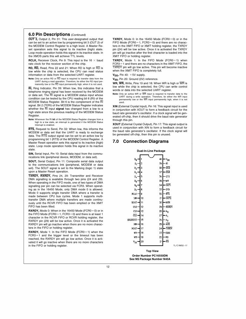
7.0 Connection Diagrams
Dual-In-Line Package
TL/C/8652–17
Top View
Order Number PC16550DN
See NS Package Number N40A
12
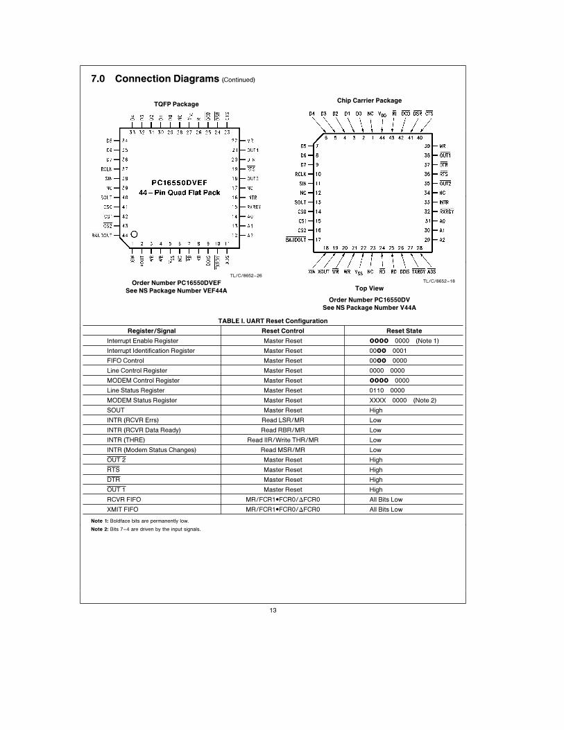
7.0 Connection Diagrams (Continued)
TQFP Package
TL/C/8652–26
Order Number PC16550DVEF
See NS Package Number VEF44A
Chip Carrier Package
TL/C/8652–18
Top View
Order Number PC16550DV
See NS Package Number V44A
TABLE I. UART Reset Configuration
Register/Signal Reset Control Reset State
Interrupt Enable Register Master Reset 0000 0000 (Note 1)
Interrupt Identification Register Master Reset 0000 0001
FIFO Control Master Reset 0000 0000
Line Control Register Master Reset 0000 0000
MODEM Control Register Master Reset 0000 0000
Line Status Register Master Reset 0110 0000
MODEM Status Register Master Reset XXXX 0000 (Note 2)
SOUT Master Reset High
INTR (RCVR Errs) Read LSR/MR Low
INTR (RCVR Data Ready) Read RBR/MR Low
INTR (THRE) Read IIR/Write THR/MR Low
INTR (Modem Status Changes) Read MSR/MR Low
OUT 2 Master Reset High
RTS Master Reset High
DTR Master Reset High
OUT 1 Master Reset High
RCVR FIFO MR/FCR1#FCR0/DFCR0 All Bits Low
XMIT FIFO MR/FCR1#FCR0/DFCR0 All Bits Low
Note 1: Boldface bits are permanently low.
Note 2: Bits 7–4 are driven by the input signals.
13
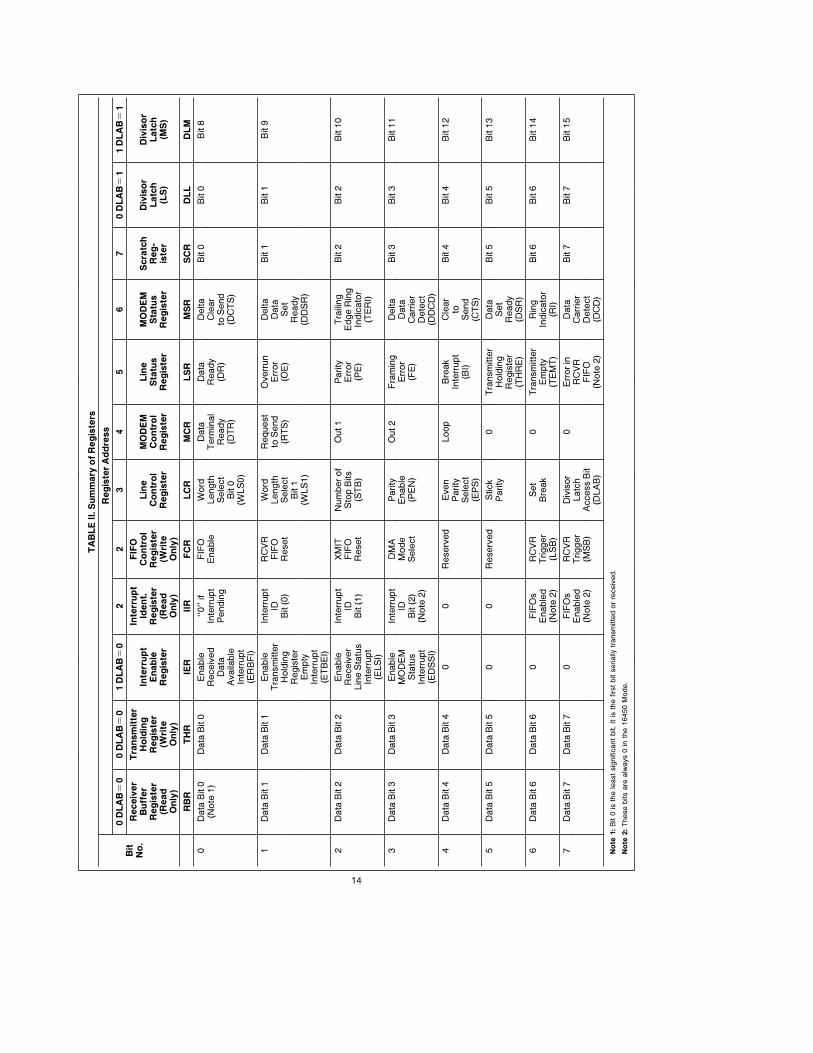
TA
BLE
II.Sum
mary
ofR
egis
ters
Regis
terA
ddre
ss
0D
LA
Be
00
DLA
Be
01
DLA
Be
02
23
45
67
0D
LA
Be
11
DLA
Be
1B
itR
eceiv
er
Tra
nsm
itte
rIn
terr
upt
FIF
ON
o.
Buff
er
Hold
ing
Inte
rrupt
Ident.
Contr
ol
Lin
eM
OD
EM
Lin
eM
OD
EM
Scra
tch
Div
isor
Div
isor
Regis
ter
Regis
ter
Enable
Regis
ter
Regis
ter
Contr
ol
Contr
ol
Sta
tus
Sta
tus
Reg-
Latc
hLatc
h(R
ead
(Write
Regis
ter
(Read
(Write
Regis
ter
Regis
ter
Regis
ter
Regis
ter
iste
r(L
S)
(MS)
Only
)O
nly
)O
nly
)O
nly
)
RB
RTH
RIE
RIIR
FC
RLC
RM
CR
LSR
MSR
SC
RD
LL
DLM
0D
ata
Bit
0D
ata
Bit
0Enable
‘‘0’’
ifFIF
OW
ord
Data
Data
Delta
Bit
0B
it0
Bit
8(N
ote
1)
Receiv
ed
Inte
rrupt
Enable
Length
Term
inal
Ready
Cle
ar
Data
Pendin
gSele
ct
Ready
(DR
)to
Send
Availa
ble
Bit
0(D
TR
)(D
CTS)
Inte
rrupt
(WLS0)
(ER
BFI)
1D
ata
Bit
1D
ata
Bit
1Enable
Inte
rrupt
RC
VR
Word
Request
Overrun
Delta
Bit
1B
it1
Bit
9Tra
nsm
itte
rID
FIF
OLength
toSend
Error
Data
Hold
ing
Bit
(0)
Reset
Sele
ct
(RTS)
(OE)
Set
Regis
ter
Bit
1R
eady
Em
pty
(WLS1)
(DD
SR
)In
terrupt
(ETB
EI)
2D
ata
Bit
2D
ata
Bit
2Enable
Inte
rrupt
XM
ITN
um
berof
Out1
Parity
Tra
iling
Bit
2B
it2
Bit
10
Receiv
er
IDFIF
OSto
pB
its
Error
Edge
Rin
gLin
eSta
tus
Bit
(1)
Reset
(STB
)(P
E)
Indic
ato
rIn
terrupt
(TER
I)(E
LSI)
3D
ata
Bit
3D
ata
Bit
3Enable
Inte
rrupt
DM
AParity
Out2
Fra
min
gD
elta
Bit
3B
it3
Bit
11
MO
DEM
IDM
ode
Enable
Error
Data
Sta
tus
Bit
(2)
Sele
ct
(PEN
)(F
E)
Carrie
rIn
terrupt
(Note
2)
Dete
ct
(ED
SSI)
(DD
CD
)
4D
ata
Bit
4D
ata
Bit
40
0R
eserv
ed
Even
Loop
Bre
ak
Cle
ar
Bit
4B
it4
Bit
12
Parity
Inte
rrupt
toSele
ct
(BI)
Send
(EPS)
(CTS)
5D
ata
Bit
5D
ata
Bit
50
0R
eserv
ed
Stick
0Tra
nsm
itte
rD
ata
Bit
5B
it5
Bit
13
Parity
Hold
ing
Set
Regis
ter
Ready
(TH
RE)
(DSR
)
6D
ata
Bit
6D
ata
Bit
60
FIF
Os
RC
VR
Set
0Tra
nsm
itte
rR
ing
Bit
6B
it6
Bit
14
Enable
dTrigger
Bre
ak
Em
pty
Indic
ato
r(N
ote
2)
(LSB
)(T
EM
T)
(RI)
7D
ata
Bit
7D
ata
Bit
70
FIF
Os
RC
VR
Div
isor
0Errorin
Data
Bit
7B
it7
Bit
15
Enable
dTrigger
Latc
hR
CVR
Carrie
r(N
ote
2)
(MSB
)A
ccess
Bit
FIF
OD
ete
ct
(DLA
B)
(Note
2)
(DC
D)
Note
1:B
it0
isth
ele
astsig
nific
antbit.It
isth
efirs
tbit
serially
transm
itte
dorre
ceiv
ed.
Note
2:These
bits
are
alw
ays
0in
the
16450
Mode.
14
8.0 RegistersThe system programmer may access any of the UART reg-
isters summarized in Table II via the CPU. These registers
control UART operations including transmission and recep-
tion of data. Each register bit in Table II has its name and
reset state shown.
8.1 LINE CONTROL REGISTER
The system programmer specifies the format of the asyn-
chronous data communications exchange and set the Divi-
sor Latch Access bit via the Line Control Register (LCR).
The programmer can also read the contents of the Line
Control Register. The read capability simplifies system pro-
gramming and eliminates the need for separate storage in
system memory of the line characteristics. Table II shows
the contents of the LCR. Details on each bit follow:
Bits 0 and 1: These two bits specify the number of bits in
each transmitted or received serial character. The encoding
of bits 0 and 1 is as follows:
Bit 1 Bit 0 Character Length
0 0 5 Bits
0 1 6 Bits
1 0 7 Bits
1 1 8 Bits
Bit 2: This bit specifies the number of Stop bits transmitted
and received in each serial character. If bit 2 is a logic 0,
one Stop bit is generated in the transmitted data. If bit 2 is a
logic 1 when a 5-bit word length is selected via bits 0 and 1,
one and a half Stop bits are generated. If bit 2 is a logic 1
when either a 6-, 7-, or 8-bit word length is selected, two
Stop bits are generated. The Receiver checks the first Stop-
bit only, regardless of the number of Stop bits selected.
Bit 3: This bit is the Parity Enable bit. When bit 3 is a logic 1,
a Parity bit is generated (transmit data) or checked (receive
data) between the last data word bit and Stop bit of the
serial data. (The Parity bit is used to produce an even or odd
number of 1s when the data word bits and the Parity bit are
summed.)
Bit 4: This bit is the Even Parity Select bit. When bit 3 is a
logic 1 and bit 4 is a logic 0, an odd number of logic 1s is
transmitted or checked in the data word bits and Parity bit.
When bit 3 is a logic 1 and bit 4 is a logic 1, an even number
of logic 1s is transmitted or checked.
Bit 5: This bit is the Stick Parity bit. When bits 3, 4 and 5 are
logic 1 the Parity bit is transmitted and checked as a logic 0.
If bits 3 and 5 are 1 and bit 4 is a logic 0 then the Parity bit is
transmitted and checked as a logic 1. If bit 5 is a logic 0
Stick Parity is disabled.
Bit 6: This bit is the Break Control bit. It causes a break
condition to be transmitted to the receiving UART. When it
is set to a logic 1, the serial output (SOUT) is forced to the
Spacing (logic 0) state. The break is disabled by setting bit 6
to a logic 0. The Break Control bit acts only on SOUT and
has no effect on the transmitter logic.
Note: This feature enables the CPU to alert a terminal in a computer com-
munications system. If the following sequence is followed, no errone-
ous or extraneous characters will be transmitted because of the
break.
1. Load an all 0s, pad character, in response to THRE.
2. Set break after the next THRE.
3. Wait for the transmitter to be idle, (TEMTe1), and clear break when
normal transmission has to be restored.
During the break, the Transmitter can be used as a character timer to accu-
rately establish the break duration.
TABLE III. Baud Rates, Divisors and Crystals
1.8432 MHz Cystal 3.072 MHz Crystal 18.432 MHz Crystal
Baud RateDecimal Divisor
Percent ErrorDecimal Divisor
Percent ErrorDecimal Divisor
Percent Errorfor 16 c Clock for 16 c Clock for 16 c Clock
50 2304 Ð 3840 Ð 23040 Ð
75 1536 Ð 2560 Ð 15360 Ð
110 1047 0.026 1745 0.026 10473 Ð
134.5 857 0.058 1428 0.034 8565 Ð
150 768 Ð 1280 Ð 7680 Ð
300 384 Ð 640 Ð 3840 Ð
600 192 Ð 320 Ð 1920 Ð
1200 96 Ð 160 Ð 920 Ð
1800 64 Ð 107 0.312 640 Ð
2000 58 0.69 96 Ð 576 Ð
2400 48 Ð 80 Ð 480 Ð
3600 32 Ð 53 0.628 320 Ð
4800 24 Ð 40 Ð 240 Ð
7200 16 Ð 27 1.23 160 Ð
9600 12 Ð 20 Ð 120 Ð
19200 6 Ð 10 Ð 60 Ð
38400 3 Ð 5 Ð 30 Ð
56000 2 2.86 Ð Ð 21 2.04
128000 Ð Ð Ð Ð 9 Ð
Note: For baud rates of 250k, 300k, 375k, 500k, 750k and 1.5M using a 24 MHz crystal causes minimal error.
15
8.0 Registers (Continued)
Bit 7: This bit is the Divisor Latch Access Bit (DLAB). It must
be set high (logic 1) to access the Divisor Latches of the
Baud Generator during a Read or Write operation. It must
be set low (logic 0) to access the Receiver Buffer, the
Transmitter Holding Register, or the Interrupt Enable Regis-
ter.
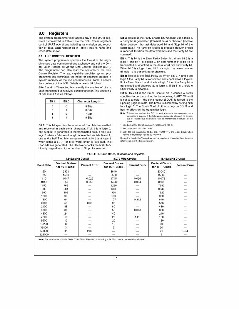
8.2 TYPICAL CLOCK CIRCUITS
TL/C/8652–19
TL/C/8652–20
Typical Crystal Oscillator Network (Note)
CRYSTAL RP RX2 C1 C2
3.1 MHz 1 MX 1.5k 10-30 pF 40-60 pF
1.8 MHz 1 MX 1.5k 10-30 pF 40-60 pF
Note: These R and C values are approximate and may vary 2x depending
on the crystal characteristics. All crystal circuits should be designed
specifically for the system.
8.3 PROGRAMMABLE BAUD GENERATOR
The UART contains a programmable Baud Generator that is
capable of taking any clock input from DC to 24 MHz and
dividing it by any divisor from 2 to 216b1. The output fre-
quency of the Baud Generator is 16 c the Baud [divisor Ýe (frequency input) d (baud rate c 16)]. Two 8-bit latches
store the divisor in a 16-bit binary format. These Divisor
Latches must be loaded during initialization to ensure prop-
er operation of the Baud Generator. Upon loading either of
the Divisor Latches, a 16-bit Baud counter is immediately
loaded.
Table III provides decimal divisors to use with crystal fre-
quencies of 1.8432 MHz, 3.072 MHz and 18.432 MHz, re-
spectively. For baud rates of 38400 and below, the error
obtained is minimal. The accuracy of the desired baud rate
is dependent on the crystal frequency chosen. Using a divi-
sor of zero is not recommended.
8.4 LINE STATUS REGISTER
This register provides status information to the CPU con-
cerning the data transfer. Table II shows the contents of the
Line Status Register. Details on each bit follow.
Bit 0: This bit is the receiver Data Ready (DR) indicator. Bit
0 is set to a logic 1 whenever a complete incoming charac-
ter has been received and transferred into the Receiver
Buffer Register or the FIFO. Bit 0 is reset to a logic 0 by
reading all of the data in the Receiver Buffer Register or the
FIFO.
Bit 1: This bit is the Overrun Error (OE) indicator. Bit 1 indi-
cates that data in the Receiver Buffer Register was not read
by the CPU before the next character was transferred into
the Receiver Buffer Register, thereby destroying the previ-
ous character. The OE indicator is set to a logic 1 upon
detection of an overrun condition and reset whenever the
CPU reads the contents of the Line Status Register. If the
FIFO mode data continues to fill the FIFO beyond the trig-
ger level, an overrun error will occur only after the FIFO is
full and the next character has been completely received in
the shift register. OE is indicated to the CPU as soon as it
happens. The character in the shift register is overwritten,
but it is not transferred to the FIFO.
Bit 2: This bit is the Parity Error (PE) indicator. Bit 2 indi-
cates that the received data character does not have the
correct even or odd parity, as selected by the even-parity-
select bit. The PE bit is set to a logic 1 upon detection of a
parity error and is reset to a logic 0 whenever the CPU reads
the contents of the Line Status Register. In the FIFO mode
this error is associated with the particular character in the
FIFO it applies to. This error is revealed to the CPU when its
associated character is at the top of the FIFO.
Bit 3: This bit is the Framing Error (FE) indicator. Bit 3 indi-
cates that the received character did not have a valid Stop
bit. Bit 3 is set to a logic 1 whenever the Stop bit following
the last data bit or parity bit is detected as a logic 0 bit
(Spacing level). The FE indicator is reset whenever the CPU
reads the contents of the Line Status Register. In the FIFO
mode this error is associated with the particular character in
the FIFO it applies to. This error is revealed to the CPU
when its associated character is at the top of the FIFO. The
UART will try to resynchronize after a framing error. To do
this it assumes that the framing error was due to the next
start bit, so it samples this ‘‘start’’ bit twice and then takes in
the ‘‘data’’.
Bit 4: This bit is the Break Interrupt (BI) indicator. Bit 4 is set
to a logic 1 whenever the received data input is held in the
Spacing (logic 0) state for longer than a full word transmis-
sion time (that is, the total time of Start bit a data bits a
Parity a Stop bits). The BI indicator is reset whenever the
CPU reads the contents of the Line Status Register. In the
FIFO mode this error is associated with the particular char-
acter in the FIFO it applies to. This error is revealed to the
CPU when its associated character is at the top of the FIFO.
When break occurs only one zero character is loaded into
the FIFO. The next character transfer is enabled after SIN
goes to the marking state and receives the next valid start
bit.
Note: Bits 1 through 4 are the error conditions that produce a Receiver Line
Status interrupt whenever any of the corresponding conditions are
detected and the interrupt is enabled.
16
8.0 Registers (Continued)
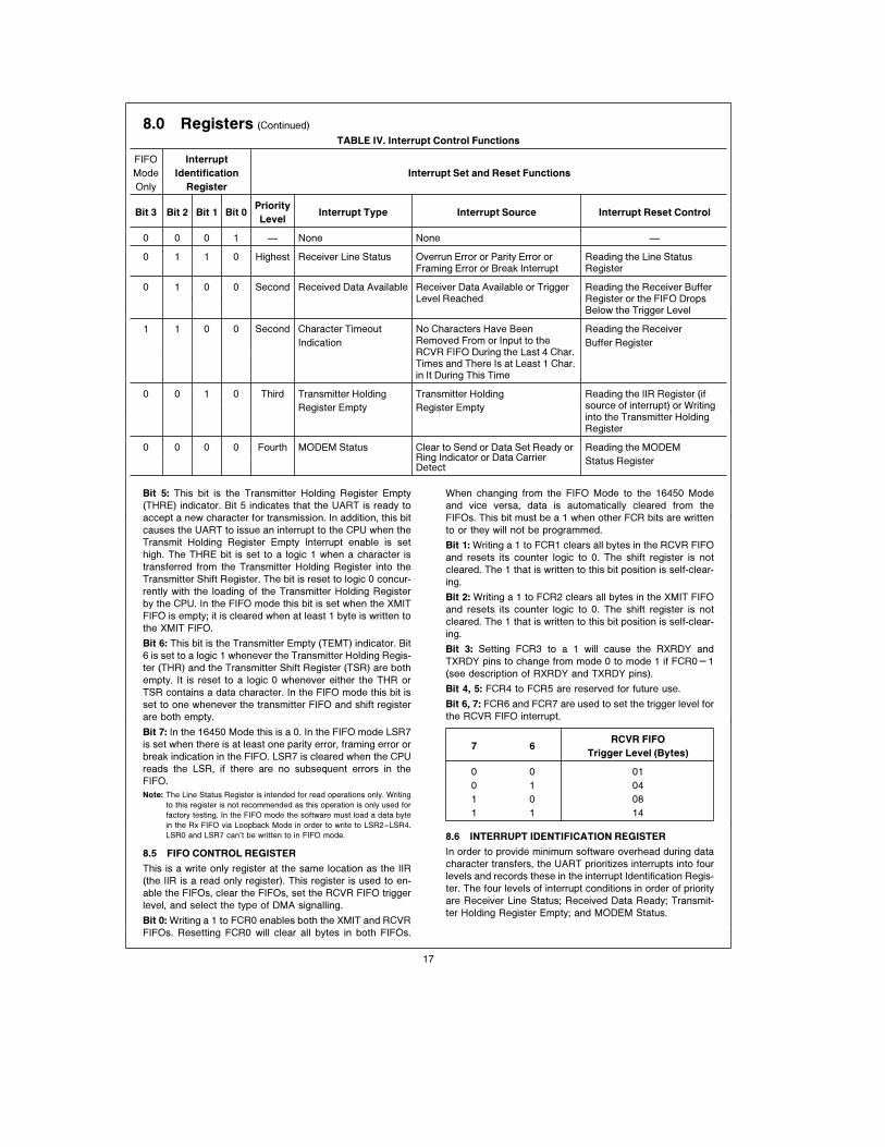
TABLE IV. Interrupt Control Functions
FIFO Interrupt
Mode Identification Interrupt Set and Reset Functions
Only Register
Bit 3 Bit 2 Bit 1 Bit 0Priority
Interrupt Type Interrupt Source Interrupt Reset ControlLevel
0 0 0 1 Ð None None Ð
0 1 1 0 Highest Receiver Line Status Overrun Error or Parity Error or Reading the Line StatusFraming Error or Break Interrupt Register
0 1 0 0 Second Received Data Available Receiver Data Available or Trigger Reading the Receiver BufferLevel Reached Register or the FIFO Drops
Below the Trigger Level
1 1 0 0 Second Character Timeout No Characters Have Been Reading the ReceiverRemoved From or Input to theIndication Buffer RegisterRCVR FIFO During the Last 4 Char.Times and There Is at Least 1 Char.in It During This Time
0 0 1 0 Third Transmitter Holding Transmitter Holding Reading the IIR Register (ifsource of interrupt) or WritingRegister Empty Register Emptyinto the Transmitter HoldingRegister
0 0 0 0 Fourth MODEM Status Clear to Send or Data Set Ready or Reading the MODEMRing Indicator or Data Carrier Status RegisterDetect
Bit 5: This bit is the Transmitter Holding Register Empty
(THRE) indicator. Bit 5 indicates that the UART is ready to
accept a new character for transmission. In addition, this bit
causes the UART to issue an interrupt to the CPU when the
Transmit Holding Register Empty Interrupt enable is set
high. The THRE bit is set to a logic 1 when a character is
transferred from the Transmitter Holding Register into the
Transmitter Shift Register. The bit is reset to logic 0 concur-
rently with the loading of the Transmitter Holding Register
by the CPU. In the FIFO mode this bit is set when the XMIT
FIFO is empty; it is cleared when at least 1 byte is written to
the XMIT FIFO.
Bit 6: This bit is the Transmitter Empty (TEMT) indicator. Bit
6 is set to a logic 1 whenever the Transmitter Holding Regis-
ter (THR) and the Transmitter Shift Register (TSR) are both
empty. It is reset to a logic 0 whenever either the THR or
TSR contains a data character. In the FIFO mode this bit is
set to one whenever the transmitter FIFO and shift register
are both empty.
Bit 7: In the 16450 Mode this is a 0. In the FIFO mode LSR7
is set when there is at least one parity error, framing error or
break indication in the FIFO. LSR7 is cleared when the CPU
reads the LSR, if there are no subsequent errors in the
FIFO.
Note: The Line Status Register is intended for read operations only. Writing
to this register is not recommended as this operation is only used for
factory testing. In the FIFO mode the software must load a data byte
in the Rx FIFO via Loopback Mode in order to write to LSR2–LSR4.
LSR0 and LSR7 can’t be written to in FIFO mode.
8.5 FIFO CONTROL REGISTER
This is a write only register at the same location as the IIR
(the IIR is a read only register). This register is used to en-
able the FIFOs, clear the FIFOs, set the RCVR FIFO trigger
level, and select the type of DMA signalling.
Bit 0: Writing a 1 to FCR0 enables both the XMIT and RCVR
FIFOs. Resetting FCR0 will clear all bytes in both FIFOs.
When changing from the FIFO Mode to the 16450 Mode
and vice versa, data is automatically cleared from the
FIFOs. This bit must be a 1 when other FCR bits are written
to or they will not be programmed.
Bit 1: Writing a 1 to FCR1 clears all bytes in the RCVR FIFO
and resets its counter logic to 0. The shift register is not
cleared. The 1 that is written to this bit position is self-clear-
ing.
Bit 2: Writing a 1 to FCR2 clears all bytes in the XMIT FIFO
and resets its counter logic to 0. The shift register is not
cleared. The 1 that is written to this bit position is self-clear-
ing.
Bit 3: Setting FCR3 to a 1 will cause the RXRDY and
TXRDY pins to change from mode 0 to mode 1 if FCR0e1
(see description of RXRDY and TXRDY pins).
Bit 4, 5: FCR4 to FCR5 are reserved for future use.
Bit 6, 7: FCR6 and FCR7 are used to set the trigger level for
the RCVR FIFO interrupt.
7 6RCVR FIFO
Trigger Level (Bytes)
0 0 01
0 1 04
1 0 08
1 1 14
8.6 INTERRUPT IDENTIFICATION REGISTER
In order to provide minimum software overhead during data
character transfers, the UART prioritizes interrupts into four
levels and records these in the interrupt Identification Regis-
ter. The four levels of interrupt conditions in order of priority
are Receiver Line Status; Received Data Ready; Transmit-
ter Holding Register Empty; and MODEM Status.
17
8.0 Registers (Continued)
When the CPU accesses the IIR, the UART freezes all inter-
rupts and indicates the highest priority pending interrupt to
the CPU. While this CPU access is occurring, the UART
records new interrupts, but does not change its current indi-
cation until the access is complete. Table II shows the con-
tents of the IIR. Details on each bit follow:
Bit 0: This bit can be used in a prioritized interrupt environ-
ment to indicate whether an interrupt is pending. When bit 0
is a logic 0, an interrupt is pending and the IIR contents may
be used as a pointer to the appropriate interrupt service
routine. When bit 0 is a logic 1, no interrupt is pending.
Bits 1 and 2: These two bits of the IIR are used to identify
the highest priority interrupt pending as indicated in Table
IV.
Bit 3: In the 16450 Mode this bit is 0. In the FIFO mode this
bit is set along with bit 2 when a timeout interrupt is pending.
Bits 4 and 5: These two bits of the IIR are always logic 0.
Bits 6 and 7: These two bits are set when FCR0e1.
8.7 INTERRUPT ENABLE REGISTER
This register enables the five types of UART interrupts.
Each interrupt can individually activate the interrupt (INTR)
output signal. It is possible to totally disable the interrupt
system by resetting bits 0 through 3 of the Interrupt Enable
Register (IER). Similarly, setting bits of the IER register to a
logic 1, enables the selected interrupt(s). Disabling an inter-
rupt prevents it from being indicated as active in the IIR and
from activating the INTR output signal. All other system
functions operate in their normal manner, including the set-
ting of the Line Status and MODEM Status Registers. Table
II shows the contents of the IER. Details on each bit follow.
Bit 0: This bit enables the Received Data Available Interrupt
(and timeout interrupts in the FIFO mode) when set to logic
1.
Bit 1: This bit enables the Transmitter Holding Register
Empty Interrupt when set to logic 1.
Bit 2: This bit enables the Receiver Line Status Interrupt
when set to logic 1.
Bit 3: This bit enables the MODEM Status Interrupt when
set to logic 1.
Bits 4 through 7: These four bits are always logic 0.
8.8 MODEM CONTROL REGISTER
This register controls the interface with the MODEM or data
set (or a peripheral device emulating a MODEM). The con-
tents of the MODEM Control Register are indicated in Table
II and are described below.
Bit 0: This bit controls the Data Terminal Ready (DTR) out-
put. When bit 0 is set to a logic 1, the DTR output is forced
to a logic 0. When bit 0 is reset to a logic 0, the DTR output
is forced to a logic 1.
Note: The DTR output of the UART may be applied to an EIA inverting line
driver (such as the DS1488) to obtain the proper polarity input at the
succeeding MODEM or data set.
Bit 1: This bit controls the Request to Send (RTS) output.
Bit 1 affects the RTS output in a manner identical to that
described above for bit 0.
Bit 2: This bit controls the Output 1 (OUT 1) signal, which is
an auxiliary user-designated output. Bit 2 affects the OUT 1
output in a manner identical to that described above for bit
0.
Bit 3: This bit controls the Output 2 (OUT 2) signal, which is
an auxiliary user-designated output. Bit 3 affects the OUT 2
output in a manner identical to that described above for bit
0.
Bit 4: This bit provides a local loopback feature for diagnos-
tic testing of the UART. When bit 4 is set to logic 1, the
following occur: the transmitter Serial Output (SOUT) is set
to the Marking (logic 1) state; the receiver Serial Input (SIN)
is disconnected; the output of the Transmitter Shift Register
is ‘‘looped back’’ into the Receiver Shift Register input; the
four MODEM Control inputs (DSR, CTS, RI, and DCD) are
disconnected; and the four MODEM Control outputs (DTR,
RTS, OUT 1, and OUT 2) are internally connected to the
four MODEM Control inputs, and the MODEM Control out-
put pins are forced to their inactive state (high). In the loop-
back mode, data that is transmitted is immediately received.
This feature allows the processor to verify the transmit-and
received-data paths of the UART.
In the loopback mode, the receiver and transmitter inter-
rupts are fully operational. Their sources are external to the
part. The MODEM Control Interrupts are also operational,
but the interrupts’ sources are now the lower four bits of the
MODEM Control Register instead of the four MODEM Con-
trol inputs. The interrupts are still controlled by the Interrupt
Enable Register.
Bits 5 through 7: These bits are permanently set to logic 0.
8.9 MODEM STATUS REGISTER
This register provides the current state of the control lines
from the MODEM (or peripheral device) to the CPU. In addi-
tion to this current-state information, four bits of the MO-
DEM Status Register provide change information. These
bits are set to a logic 1 whenever a control input from the
MODEM changes state. They are reset to logic 0 whenever
the CPU reads the MODEM Status Register.
The contents of the MODEM Status Register are indicated
in Table II and described below.
Bit 0: This bit is the Delta Clear to Send (DCTS) indicator.
Bit 0 indicates that the CTS input to the chip has changed
state since the last time it was read by the CPU.
Bit 1: This bit is the Delta Data Set Ready (DDSR) indicator.
Bit 1 indicates that the DSR input to the chip has changed
state since the last time it was read by the CPU.
Bit 2: This bit is the Trailing Edge of Ring Indicator (TERI)
detector. Bit 2 indicates that the RI input to the chip has
changed from a low to a high state.
Bit 3: This bit is the Delta Data Carrier Detect (DDCD) indi-
cator. Bit 3 indicates that the DCD input to the chip has
changed state.
Note: Whenever bit 0, 1, 2, or 3 is set to logic 1, a MODEM Status Interrupt
is generated.
Bit 4: This bit is the complement of the Clear to Send (CTS)
input. If bit 4 (loop) of the MCR is set to a 1, this bit is
equivalent to RTS in the MCR.
Bit 5: This bit is the complement of the Data Set Ready
(DSR) input. If bit 4 of the MCR is set to a 1, this bit is
equivalent to DTR in the MCR.
Bit 6: This bit is the complement of the Ring Indicator (RI)
input. If bit 4 of the MCR is set to a 1, this bit is equivalent to
OUT 1 in the MCR.
18
8.0 Registers (Continued)
Bit 7: This bit is the complement of the Data Carrier Detect
(DCD) input. If bit 4 of the MCR is set to a 1, this bit is
equivalent to OUT 2 in the MCR.
8.10 SCRATCHPAD REGISTER
This 8-bit Read/Write Register does not control the UART
in anyway. It is intended as a scratchpad register to be used
by the programmer to hold data temporarily.
8.11 FIFO INTERRUPT MODE OPERATION
When the RCVR FIFO and receiver interrupts are enabled
(FCR0e1, IER0e1) RCVR interrupts will occur as follows:
A. The receive data available interrupt will be issued to the
CPU when the FIFO has reached its programmed trigger
level; it will be cleared as soon as the FIFO drops below
its programmed trigger level.
B. The IIR receive data available indication also occurs
when the FIFO trigger level is reached, and like the inter-
rupt it is cleared when the FIFO drops below the trigger
level.
C. The receiver line status interrupt (IIRe06), as before,
has higher priority than the received data available
(IIRe04) interrupt.
D. The data ready bit (LSR0) is set as soon as a character is
transferred from the shift register to the RCVR FIFO. It is
reset when the FIFO is empty.
When RCVR FIFO and receiver interrupts are enabled,
RCVR FIFO timeout interrupts will occur as follows:
A. A FIFO timeout interrupt will occur, if the following condi-
tions exist:
Ð at least one character is in the FIFO
Ð the most recent serial character received was
longer than 4 continuous character times ago (if 2
stop bits are programmed the second one is in-
cluded in this time delay).
Ð the most recent CPU read of the FIFO was longer
than 4 continuous character times ago.
The maximum time between a received character and a
timeout interrupt will be 160 ms at 300 baud with a 12-bit
receive character (i.e., 1 Start, 8 Data, 1 Parity and 2 Stop
Bits).
B. Character times are calculated by using the RCLK input
for a clock signal (this makes the delay proportional to
the baudrate).
C. When a timeout interrupt has occurred it is cleared and
the timer reset when the CPU reads one character from
the RCVR FIFO.
D. When a timeout interrupt has not occurred the timeout
timer is reset after a new character is received or after
the CPU reads the RCVR FIFO.
When the XMIT FIFO and transmitter interrupts are enabled
(FCR0e1, IER1e1), XMIT interrupts will occur as follows:
A. The transmitter holding register interrupt (02) occurs
when the XMIT FIFO is empty; it is cleared as soon as
the transmitter holding register is written to (1 to 16 char-
acters may be written to the XMIT FIFO while servicing
this interrupt) or the IIR is read.
B. The transmitter FIFO empty indications will be delayed 1
character time minus the last stop bit time whenever the
following occurs: THREe1 and there have not been at
least two bytes at the same time in the transmit FIFO,
since the last THREe1. The first transmitter interrupt af-
ter changing FCR0 will be immediate, if it is enabled.
Character timeout and RCVR FIFO trigger level interrupts
have the same priority as the current received data avail-
able interrupt; XMIT FIFO empty has the same priority as
the current transmitter holding register empty interrupt.
8.12 FIFO POLLED MODE OPERATION
With FCR0e1 resetting IER0, IER1, IER2, IER3 or all to
zero puts the UART in the FIFO Polled Mode of operation.
Since the RCVR and XMITTER are controlled separately
either one or both can be in the polled mode of operation.
In this mode the user’s program will check RCVR and XMIT-
TER status via the LSR. As stated previously:
LSR0 will be set as long as there is one byte in the RCVR
FIFO.
LSR1 to LSR4 will specify which error(s) has occurred.
Character error status is handled the same way as when
in the interrupt mode, the IIR is not affected since
IER2e0.
LSR5 will indicate when the XMIT FIFO is empty.
LSR6 will indicate that both the XMIT FIFO and shift reg-
ister are empty.
LSR7 will indicate whether there are any errors in the
RCVR FIFO.
There is no trigger level reached or timeout condition indi-
cated in the FIFO Polled Mode, however, the RCVR and
XMIT FIFOs are still fully capable of holding characters.
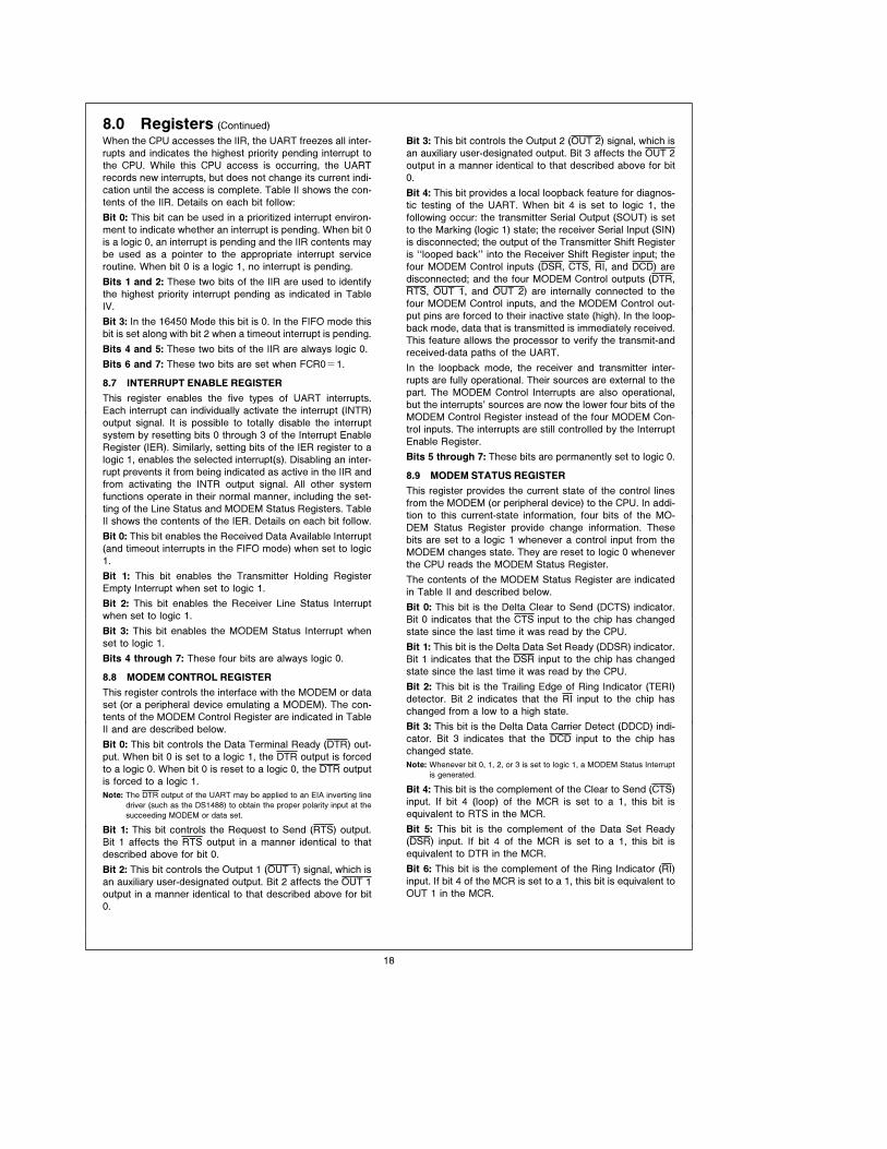
9.0 Typical Applications
Typical Interface for a
High-Capacity Data Bus
TL/C/8652–23
19
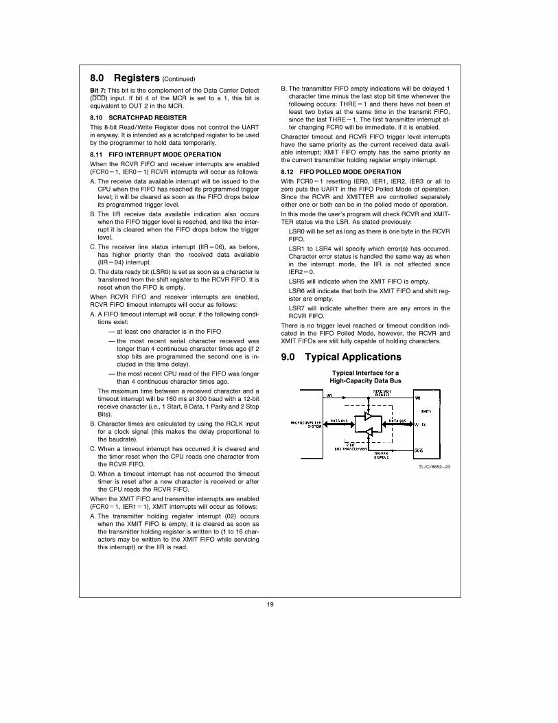
9.0 Typical Applications (Continued)
This
show
sth
ebasic
connections
ofan
PC
16550D
toan
8088
CPU
TL/C
/8652–22
20
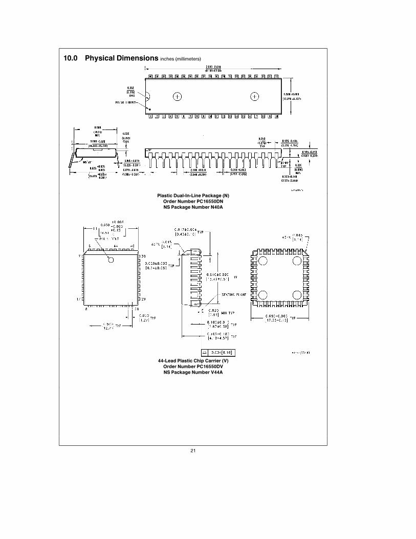
10.0 Physical Dimensions inches (millimeters)
Plastic Dual-In-Line Package (N)
Order Number PC16550DN
NS Package Number N40A
44-Lead Plastic Chip Carrier (V)
Order Number PC16550DV
NS Package Number V44A
21
PC
16550D
Univ
ers
alA
synchro
nous
Receiv
er/
Tra
nsm
itte
rw
ith
FIF
Os
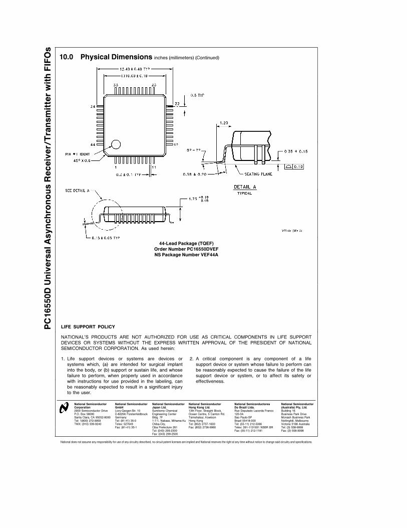
10.0 Physical Dimensions inches (millimeters) (Continued)
44-Lead Package (TQEF)
Order Number PC16550DVEF
NS Package Number VEF44A
LIFE SUPPORT POLICY
NATIONAL’S PRODUCTS ARE NOT AUTHORIZED FOR USE AS CRITICAL COMPONENTS IN LIFE SUPPORT
DEVICES OR SYSTEMS WITHOUT THE EXPRESS WRITTEN APPROVAL OF THE PRESIDENT OF NATIONAL
SEMICONDUCTOR CORPORATION. As used herein:
1. Life support devices or systems are devices or 2. A critical component is any component of a life
systems which, (a) are intended for surgical implant support device or system whose failure to perform can
into the body, or (b) support or sustain life, and whose be reasonably expected to cause the failure of the life
failure to perform, when properly used in accordance support device or system, or to affect its safety or
with instructions for use provided in the labeling, can effectiveness.
be reasonably expected to result in a significant injury
to the user.
National Semiconductor National Semiconductor National Semiconductor National Semiconductor National Semiconductores National SemiconductorCorporation GmbH Japan Ltd. Hong Kong Ltd. Do Brazil Ltda. (Australia) Pty, Ltd.2900 Semiconductor Drive Livry-Gargan-Str. 10 Sumitomo Chemical 13th Floor, Straight Block, Rue Deputado Lacorda Franco Building 16P.O. Box 58090 D-82256 F 4urstenfeldbruck Engineering Center Ocean Centre, 5 Canton Rd. 120-3A Business Park DriveSanta Clara, CA 95052-8090 Germany Bldg. 7F Tsimshatsui, Kowloon Sao Paulo-SP Monash Business ParkTel: 1(800) 272-9959 Tel: (81-41) 35-0 1-7-1, Nakase, Mihama-Ku Hong Kong Brazil 05418-000 Nottinghill, MelbourneTWX: (910) 339-9240 Telex: 527649 Chiba-City, Tel: (852) 2737-1600 Tel: (55-11) 212-5066 Victoria 3168 Australia
Fax: (81-41) 35-1 Ciba Prefecture 261 Fax: (852) 2736-9960 Telex: 391-1131931 NSBR BR Tel: (3) 558-9999Tel: (043) 299-2300 Fax: (55-11) 212-1181 Fax: (3) 558-9998Fax: (043) 299-2500
National does not assume any responsibility for use of any circuitry described, no circuit patent licenses are implied and National reserves the right at any time without notice to change said circuitry and specifications.