design of asynchronous interconnect network for …kstevens/6770/reports/07-async-noc.pdfdesign of...
TRANSCRIPT

Final Report for ECE 6770 Project
Design of Asynchronous Interconnect Network for SoC
Hosuk Han1
May 12, 2007
1Team leader

Contents
1 Introduction 1
2 Project Overview 2
2.1 Asynchronous Network Fabric . . . . . . . . . . . . . . . . . . . . . . . . . . . .3
2.2 Interface circuit: FIFO and Synchronizer . . . . . . . . . . . . . . . . . . . . . . .3
2.3 Processing Element . . . . . . . . . . . . . . . . . . . . . . . . . . . . . . . . . .3
3 Asynchronous Network Fabric Design 4
3.1 Switch Module . . . . . . . . . . . . . . . . . . . . . . . . . . . . . . . . . . . .4
3.1.1 PetrifyVersion . . . . . . . . . . . . . . . . . . . . . . . . . . . . . . . . 4
3.1.2 3D Version . . . . . . . . . . . . . . . . . . . . . . . . . . . . . . . . . . 6
3.2 Join Module . . . . . . . . . . . . . . . . . . . . . . . . . . . . . . . . . . . . . .7
3.3 Design Issues . . . . . . . . . . . . . . . . . . . . . . . . . . . . . . . . . . . . .9
3.4 Circuit and Layout . . . . . . . . . . . . . . . . . . . . . . . . . . . . . . . . . .9
3.4.1 Switch Module . . . . . . . . . . . . . . . . . . . . . . . . . . . . . . . .10
3.4.2 Join Module . . . . . . . . . . . . . . . . . . . . . . . . . . . . . . . . .11
3.4.3 Asynchronous Router . . . . . . . . . . . . . . . . . . . . . . . . . . . . .13
4 Asynchronous FIFOs 14
4.1 Asynchronous Circuit Modules . . . . . . . . . . . . . . . . . . . . . . . . . . . .14
4.1.1 Linear Module . . . . . . . . . . . . . . . . . . . . . . . . . . . . . . . .14
4.1.2 Toggle Module . . . . . . . . . . . . . . . . . . . . . . . . . . . . . . . .15
4.1.3 Merge Module . . . . . . . . . . . . . . . . . . . . . . . . . . . . . . . .16
4.2 Different Structural FIFOs . . . . . . . . . . . . . . . . . . . . . . . . . . . . . .18
4.2.1 Linear FIFO . . . . . . . . . . . . . . . . . . . . . . . . . . . . . . . . .18
4.2.2 Parallel FIFO . . . . . . . . . . . . . . . . . . . . . . . . . . . . . . . . .18
4.2.3 Tree FIFO . . . . . . . . . . . . . . . . . . . . . . . . . . . . . . . . . . .19
4.2.4 Square FIFO . . . . . . . . . . . . . . . . . . . . . . . . . . . . . . . . .19
4.3 Performance Comparison . . . . . . . . . . . . . . . . . . . . . . . . . . . . . . .20
4.4 Conclusion . . . . . . . . . . . . . . . . . . . . . . . . . . . . . . . . . . . . . .21
5 Behavioral Validation & Results 22
5.1 Golden Model & Testbench . . . . . . . . . . . . . . . . . . . . . . . . . . . . . .22
6 Conclusion & Further Researches 22
i

A Petrify Input Files 25
A.1 Asynchronous Network Fabric Modules . . . . . . . . . . . . . . . . . . . . . . .25
A.1.1 Switch.g . . . . . . . . . . . . . . . . . . . . . . . . . . . . . . . . . . .25
A.1.2 Join.g . . . . . . . . . . . . . . . . . . . . . . . . . . . . . . . . . . . . .26
ii
List of Figures
1 System Level Block Digram . . . . . . . . . . . . . . . . . . . . . . . . . . . . .2
2 Chip Level Block Diagram . . . . . . . . . . . . . . . . . . . . . . . . . . . . . .2
3 Router Block Diagram . . . . . . . . . . . . . . . . . . . . . . . . . . . . . . . .3
4 Interface of Switch Module, Petrify Version . . . . . . . . . . . . . . . . . . . . .4
5 Petri-net for Switch . . . . . . . . . . . . . . . . . . . . . . . . . . . . . . . . . .5
6 Interface of Switch Module, 3D Version . . . . . . . . . . . . . . . . . . . . . . .6
7 Extended Burst Mode FSM for Switch . . . . . . . . . . . . . . . . . . . . . . . .6
8 Interface of Join Module . . . . . . . . . . . . . . . . . . . . . . . . . . . . . . .7
9 Petri-net for Join . . . . . . . . . . . . . . . . . . . . . . . . . . . . . . . . . . .8
10 Circuit for Switch . . . . . . . . . . . . . . . . . . . . . . . . . . . . . . . . . . .9
11 Circuit for Switch Controller . . . . . . . . . . . . . . . . . . . . . . . . . . . . .9
12 Circuit for Switch Module Test . . . . . . . . . . . . . . . . . . . . . . . . . . . .10
13 Simulation of Switch Module . . . . . . . . . . . . . . . . . . . . . . . . . . . . .10
14 Layout of Switch Module . . . . . . . . . . . . . . . . . . . . . . . . . . . . . . .11
15 Circuit for Join . . . . . . . . . . . . . . . . . . . . . . . . . . . . . . . . . . . .11
16 Circuit for Join controller . . . . . . . . . . . . . . . . . . . . . . . . . . . . . . .12
17 Simulation of Join Module . . . . . . . . . . . . . . . . . . . . . . . . . . . . . .12
18 Layout of Join Module . . . . . . . . . . . . . . . . . . . . . . . . . . . . . . . .13
19 Layout of Async Router . . . . . . . . . . . . . . . . . . . . . . . . . . . . . . . .13
20 Linear Module . . . . . . . . . . . . . . . . . . . . . . . . . . . . . . . . . . . .14
21 Linear Module’s Petri-net and STG . . . . . . . . . . . . . . . . . . . . . . . . . .15
22 Toggle Module . . . . . . . . . . . . . . . . . . . . . . . . . . . . . . . . . . . .15
23 Toggle Petri-net and STG . . . . . . . . . . . . . . . . . . . . . . . . . . . . . . .16
24 Merge Module . . . . . . . . . . . . . . . . . . . . . . . . . . . . . . . . . . . .17
25 Merge Module’s Petri-net and STG . . . . . . . . . . . . . . . . . . . . . . . . . .17
26 Linear Asynchronous FIFO . . . . . . . . . . . . . . . . . . . . . . . . . . . . . .18
27 Parallel Asynchronous FIFO . . . . . . . . . . . . . . . . . . . . . . . . . . . . .18
28 Tree Asynchronous FIFO . . . . . . . . . . . . . . . . . . . . . . . . . . . . . . .19
29 Square Asynchronous FIFO . . . . . . . . . . . . . . . . . . . . . . . . . . . . .19
30 Various FIFO’s waveform for latency . . . . . . . . . . . . . . . . . . . . . . . . .20
31 Testbench Model . . . . . . . . . . . . . . . . . . . . . . . . . . . . . . . . . . .22
iii

1 Introduction
As System-on-Chip (SoC) design is getting complicated, communication between many compo-nents in SoC is becoming more difficult and important. Furthermore, the wire delay compared togate delay becomes more significant. The performance of SoC therefore highly depends on that ofthe interconnect architecture. Besides high performance and low power operation, a new intercon-nect architecture should have ability to connect synchronous blocks which have different operationfrequencies since each IP block in current SoC may operate its own frequency.
Interconnect system for SoC can be designed with either synchronous or asynchronous design tech-nique. Sufficiently enough support of industrial CAD tools in synchronous design process enablesfast and reliable design and verification of synchronous system and high coverage of testability ofdesign. However, global clock problems of synchronous system, such as clock distribution, clockskew problem, are getting worse in SoC design for providing one global clock signal in whole SoCsystem. Furthermore, this global clock issue prevents predesigned IP blocks from operating withtheir optimized clock frequencies. Every IP block should be modified its operating clock frequencymatching with global clock. As an alternative method, a synchronizer can be used between twoclock systems, synchronous interconnect system and each synchronous IP block. But, usually asynchronizer between two clock systems is more complicated and causes more synchronizing costthan between an asynchronous system and a synchronous system.
On the other hand, asynchronous design does not have support with well-developed CAD tools asmuch as synchronous design. It leads that designers need to spend more time to design and verifytheir circuits or systems. Asynchronous design is also suffering from testability problem. But,generally asynchronous design provides higher performance and lower power operation comparedwith synchronous design. Asynchronous interconnect system in SoC design promises several ad-vantages that compensate its disadvantages and surpass the advantages of synchronous intercon-nect system. With asynchronous interconnect system, SoC system does not require one globalclock in whole system any more. It leads to elimination or reduction of any global clock distribu-tion and clock skew problem. The more valuable benefit is that predesigned synchronous IP blockcan be utilized with its operating frequency optimized for its own power and performance.
From the perspective of the characteristics of interconnect system in SoC, Globally AsynchronousLocally Synchronous (GALS) system is viewed as a promising solution for SoC design. In GALSsystems, each synchronous IP core operates with local frequency and asynchronous interconnec-tion is used for enabling each clock domain to communicate with each other. It means that GALSsystem can make use of the advantages of asynchronous interconnect system as aforementioned.
The ultimate goal of this project is to implement a simple GALS system made up of several simpleprocessing elements (PEs), interface circuits and an asynchronous network fabric for evaluatingthe performance of our new network fabric. PEs generate network traffic in the network fabric.Interface circuit will support to connect between synchronous PEs and asynchronous network fab-ric. This project can be seen as a revised version of ECE6710 class project in which synchronousnetwork fabric and other elements were designed. We can compare performance and other factorsbetween synchronous interconnect system and asynchronous one after completing this project.
1
2 Project Overview
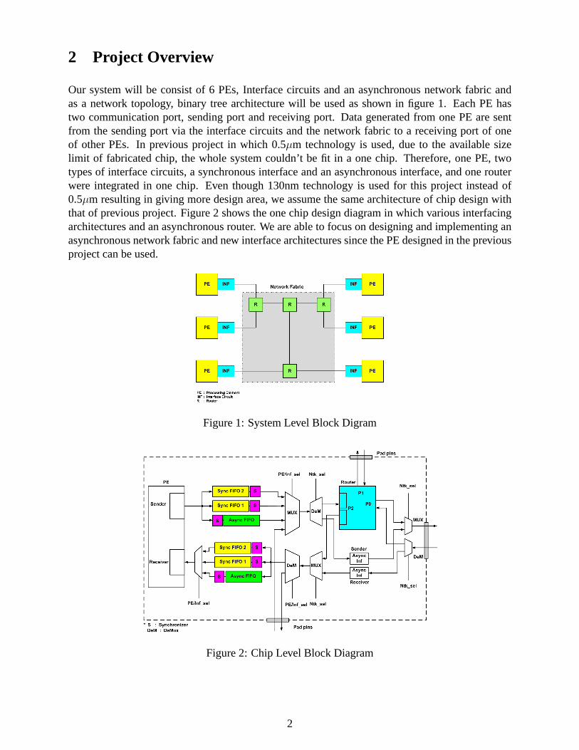
Our system will be consist of 6 PEs, Interface circuits and an asynchronous network fabric andas a network topology, binary tree architecture will be used as shown in figure 1. Each PE hastwo communication port, sending port and receiving port. Data generated from one PE are sentfrom the sending port via the interface circuits and the network fabric to a receiving port of oneof other PEs. In previous project in which 0.5µm technology is used, due to the available sizelimit of fabricated chip, the whole system couldn’t be fit in a one chip. Therefore, one PE, twotypes of interface circuits, a synchronous interface and an asynchronous interface, and one routerwere integrated in one chip. Even though 130nm technology is used for this project instead of0.5µm resulting in giving more design area, we assume the same architecture of chip design withthat of previous project. Figure 2 shows the one chip design diagram in which various interfacingarchitectures and an asynchronous router. We are able to focus on designing and implementing anasynchronous network fabric and new interface architectures since the PE designed in the previousproject can be used.
Figure 1: System Level Block Digram
Figure 2: Chip Level Block Diagram
2
2.1 Asynchronous Network Fabric
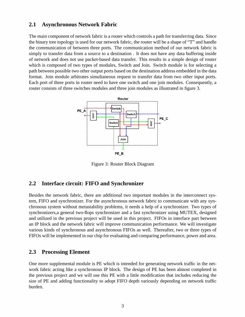
The main component of network fabric is a router which controls a path for transferring data. Sincethe binary tree topology is used for our network fabric, the router will be a shape of “T” and handlethe communication of between three ports. The communication method of our network fabric issimply to transfer data from a source to a destination . It does not have any data buffering insideof network and does not use packet-based data transfer. This results in a simple design of routerwhich is composed of two types of modules, Switch and Join. Switch module is for selecting apath between possible two other output ports based on the destination address embedded in the dataformat. Join module arbitrates simultaneous request to transfer data from two other input ports.Each port of three ports in router need to have one switch and one join modules. Consequently, arouter consists of three switches modules and three join modules as illustrated in figure 3.
Figure 3: Router Block Diagram
2.2 Interface circuit: FIFO and Synchronizer
Besides the network fabric, there are additional two important modules in the interconnect sys-tem, FIFO and synchronizer. For the asynchronous network fabric to communicate with any syn-chronous system without metastability problems, it needs a help of a synchronizer. Two types ofsynchronizers,a general two-flops synchronizer and a fast synchronizer using MUTEX, designedand utilized in the previous project will be used in this project. FIFOs in interface part betweenan IP block and the network fabric will improve communication performance. We will investigatevarious kinds of synchronous and asynchronous FIFOs as well. Thereafter, two or three types ofFIFOs will be implemented in our chip for evaluating and comparing performance, power and area.
2.3 Processing Element
One more supplemental module is PE which is intended for generating network traffic in the net-work fabric acting like a synchronous IP block. The design of PE has been almost completed inthe previous project and we will use this PE with a little modification that includes reducing thesize of PE and adding functionality to adopt FIFO depth variously depending on network trafficburden.
3
3 Asynchronous Network Fabric Design
Among various tools for asynchronous circuit design, we chose to usePetrify. After we defined aspecification of each functional module in CCS [3], a petri-net was generated based on the speci-fication and it was converted to the input file format ofPetrify.
Two asynchronous modules, switch module and join module, were designed as components for therouter of the network fabric. The same handshake protocol of the asynchronous FIFO controller in[4] were basically used in designing these two modules.
3.1 Switch Module
3.1.1 PetrifyVersion
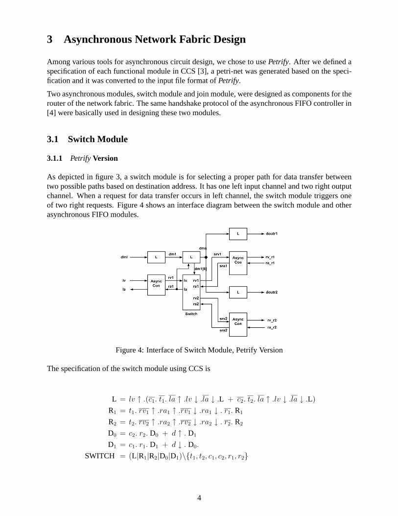
As depicted in figure 3, a switch module is for selecting a proper path for data transfer betweentwo possible paths based on destination address. It has one left input channel and two right outputchannel. When a request for data transfer occurs in left channel, the switch module triggers oneof two right requests. Figure 4 shows an interface diagram between the switch module and otherasynchronous FIFO modules.
Figure 4: Interface of Switch Module, Petrify Version
The specification of the switch module using CCS is
L = lv ↑ .(c1. t1. la ↑ .lv ↓ .la ↓ .L + c2. t2. la ↑ .lv ↓ .la ↓ .L)
R1 = t1. rv1 ↑ .ra1 ↑ .rv1 ↓ .ra1 ↓ . r1. R1
R2 = t2. rv2 ↑ .ra2 ↑ .rv2 ↓ .ra2 ↓ . r2. R2
D0 = c2. r2. D0 + d ↑ . D1
D1 = c1. r1. D1 + d ↓ . D0.
SWITCH = (L|R1|R2|D0|D1)\{t1, t2, c1, c2, r1, r2}
4
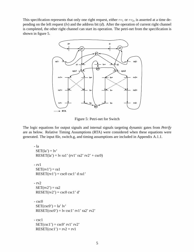
This specification represents that only one right request, eitherrv1 or rv2, is asserted at a time de-pending on the left request (lv) and the address bit (d). After the operation of current right channelis completed, the other right channel can start its operation. The petri-net from the specification isshown in figure 5.
Figure 5: Petri-net for Switch
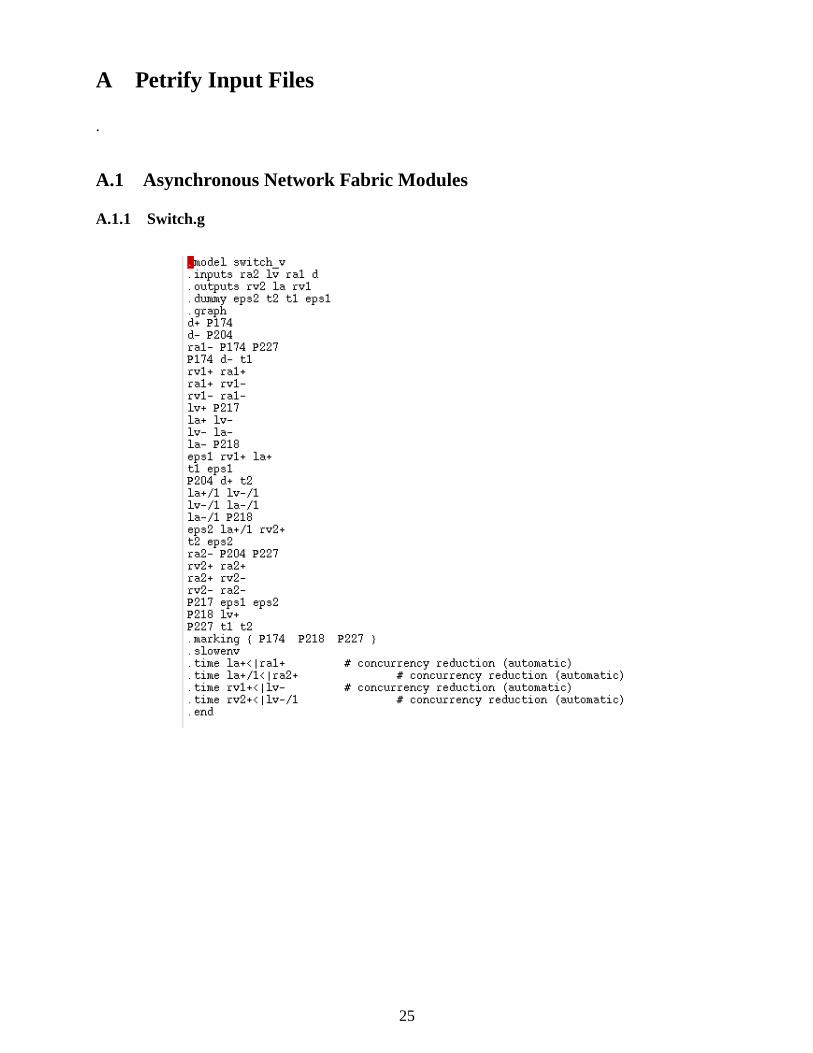
The logic equations for output signals and internal signals targeting dynamic gates fromPetrifyare as below. Relative Timing Assumptions (RTA) were considered when these equations weregenerated. The input file, switch.g, and timing assumptions are included in Appendix A.1.1.
- laSET(la’) = lv’RESET(la’) = lv ra1’ (rv1’ ra2’ rv2’ + csc0)
- rv1SET(rv1’) = ra1RESET(rv1’) = csc0 csc1’ d ra1’
- rv2SET(rv2’) = ra2RESET(rv2’) = csc0 csc1’ d’
- csc0SET(csc0’) = la’ lv’RESET(csc0’) = lv csc1’ rv1’ ra2’ rv2’
- csc1SET(csc1’) = csc0’ rv1’ rv2’RESET(csc1’) = rv2 + rv1
5
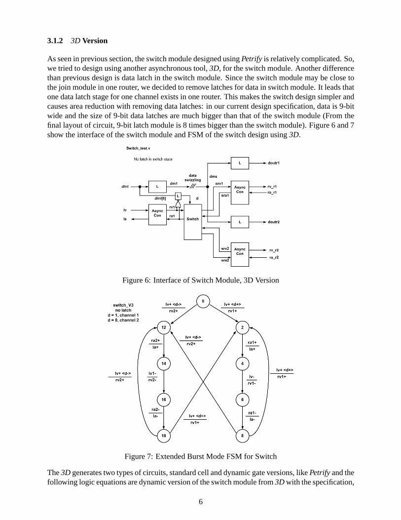
3.1.2 3D Version
As seen in previous section, the switch module designed usingPetrify is relatively complicated. So,we tried to design using another asynchronous tool,3D, for the switch module. Another differencethan previous design is data latch in the switch module. Since the switch module may be close tothe join module in one router, we decided to remove latches for data in switch module. It leads thatone data latch stage for one channel exists in one router. This makes the switch design simpler andcauses area reduction with removing data latches: in our current design specification, data is 9-bitwide and the size of 9-bit data latches are much bigger than that of the switch module (From thefinal layout of circuit, 9-bit latch module is 8 times bigger than the switch module). Figure 6 and 7show the interface of the switch module and FSM of the switch design using3D.
Figure 6: Interface of Switch Module, 3D Version
Figure 7: Extended Burst Mode FSM for Switch
The3D generates two types of circuits, standard cell and dynamic gate versions, likePetrifyand thefollowing logic equations are dynamic version of the switch module from3Dwith the specification,
6
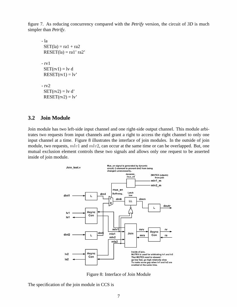
figure 7. As reducing concurrency compared with thePetrify version, the circuit of3D is muchsimpler thanPetrify.
- laSET(la) = ra1 + ra2RESET(la) = ra1’ ra2’
- rv1SET(rv1) = lv dRESET(rv1) = lv’
- rv2SET(rv2) = lv d’RESET(rv2) = lv’
3.2 Join Module
Join module has two left-side input channel and one right-side output channel. This module arbi-trates two requests from input channels and grant a right to access the right channel to only oneinput channel at a time. Figure 8 illustrates the interface of join modules. In the outside of joinmodule, two requests,mlv1 andmlv2, can occur at the same time or can be overlapped. But, onemutual exclusion element controls these two signals and allows only one request to be assertedinside of join module.
Figure 8: Interface of Join Module
The specification of the join module in CCS is
7
L1 = t1 .lv1 ↑ .c1. la1 ↑ .lv1 ↓ .la1 ↓ .x1 .L1
L2 = t2 .lv2 ↑ .c2. la2 ↑ .lv2 ↓ .la2 ↓ .x2 .L2
R = c1. rv ↑ .ra ↑ .rv ↓ .ra ↓ .R + c2. rv ↑ .ra ↑ .rv ↓ .ra ↓ .R
ME = t1 .x1 .ME + t2 .x2 .ME
JOIN = (L1|L2|R|ME)\{t1, t2, x1, x2}.
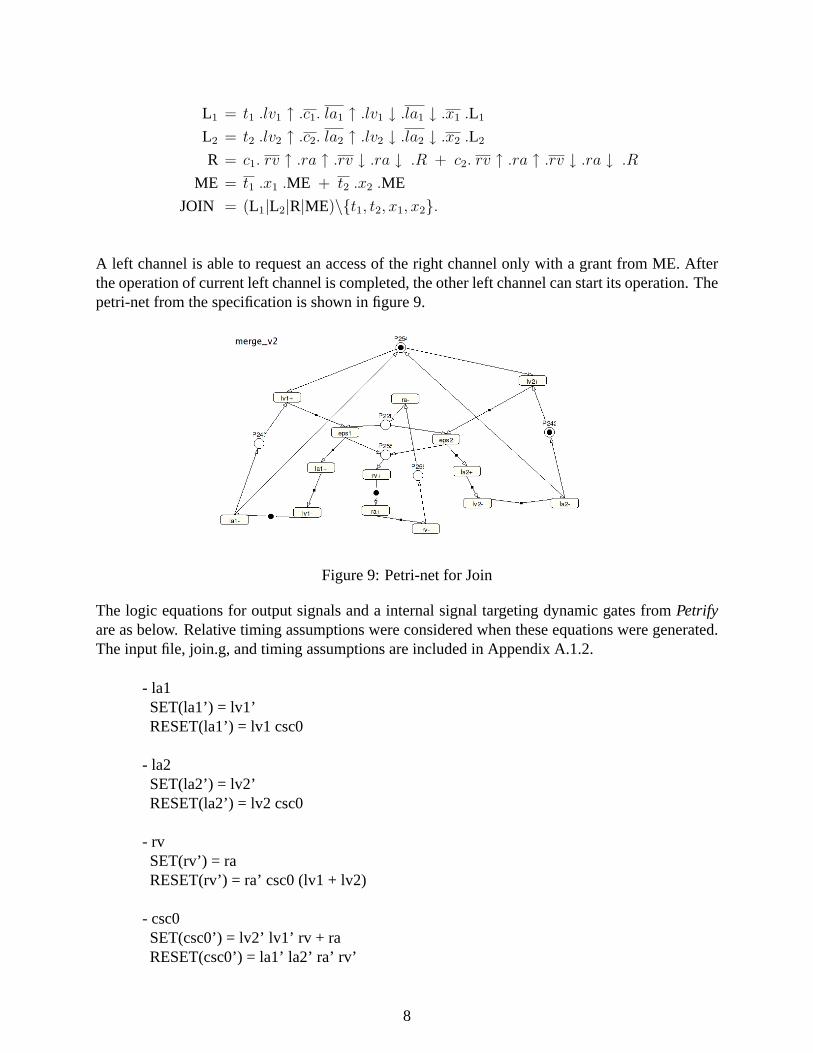
A left channel is able to request an access of the right channel only with a grant from ME. Afterthe operation of current left channel is completed, the other left channel can start its operation. Thepetri-net from the specification is shown in figure 9.
Figure 9: Petri-net for Join
The logic equations for output signals and a internal signal targeting dynamic gates fromPetrifyare as below. Relative timing assumptions were considered when these equations were generated.The input file, join.g, and timing assumptions are included in Appendix A.1.2.
- la1SET(la1’) = lv1’RESET(la1’) = lv1 csc0
- la2SET(la2’) = lv2’RESET(la2’) = lv2 csc0
- rvSET(rv’) = raRESET(rv’) = ra’ csc0 (lv1 + lv2)
- csc0SET(csc0’) = lv2’ lv1’ rv + raRESET(csc0’) = la1’ la2’ ra’ rv’
8
3.3 Design Issues
The switch module and join module were designed usingPetrify first. But, the generated dynamicgates are still too complex to be built and to analyze operation timing. In some cases, more than5 transistors need to be connected in series. It might cause an area problem in order to get anominal FO4 delay. So, another tool,3D, designed for burst mode asynchronous circuits is usedfor getting simpler circuit thanPetrify. As a result, for the switch module circuit,3D version circuitwas chosen since it had simpler implementation with modifying specification. Meanwhile, the 3Dversion for the join module was similar to that ofPetrify in circuit complexity. Therefore, for thejoin module, we decided to usePetrifyversion.
3.4 Circuit and Layout
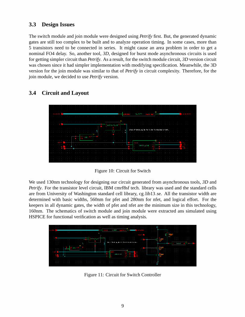
Figure 10: Circuit for Switch
We used 130nm technology for designing our circuit generated from asynchronous tools,3D andPetrify. For the transistor level circuit, IBM cmrf8sf tech. library was used and the standard cellsare from University of Washington standard cell library, cglib13 se. All the transistor width aredetermined with basic widths, 560nm for pfet and 280nm for nfet, and logical effort. For thekeepers in all dynamic gates, the width of pfet and nfet are the minimum size in this technology,160nm. The schematics of switch module and join module were extracted ans simulated usingHSPICE for functional verification as well as timing analysis.
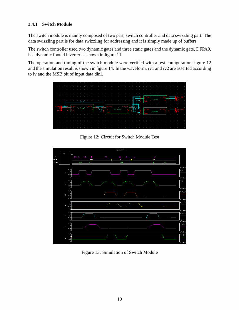
Figure 11: Circuit for Switch Controller
9
3.4.1 Switch Module
The switch module is mainly composed of two part, switch controller and data swizzling part. Thedata swizzling part is for data swizzling for addressing and it is simply made up of buffers.
The switch controller used two dynamic gates and three static gates and the dynamic gate, DFPA0,is a dynamic footed inverter as shown in figure 11.
The operation and timing of the switch module were verified with a test configuration, figure 12and the simulation result is shown in figure 14. In the waveform, rv1 and rv2 are asserted accordingto lv and the MSB bit of input data dinl.
Figure 12: Circuit for Switch Module Test
Figure 13: Simulation of Switch Module
10
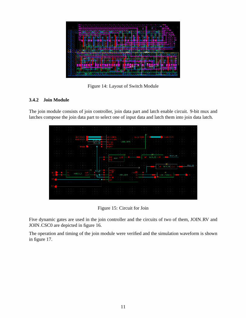
Figure 14: Layout of Switch Module
3.4.2 Join Module
The join module consists of join controller, join data part and latch enable circuit. 9-bit mux andlatches compose the join data part to select one of input data and latch them into join data latch.
Figure 15: Circuit for Join
Five dynamic gates are used in the join controller and the circuits of two of them, JOINRV andJOIN CSC0 are depicted in figure 16.
The operation and timing of the join module were verified and the simulation waveform is shownin figure 17.
11
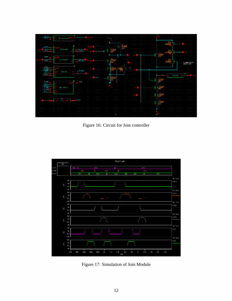
Figure 16: Circuit for Join controller
Figure 17: Simulation of Join Module
12
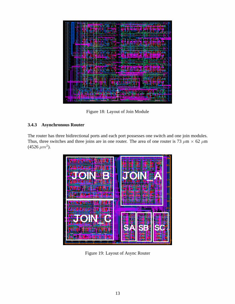
Figure 18: Layout of Join Module
3.4.3 Asynchronous Router
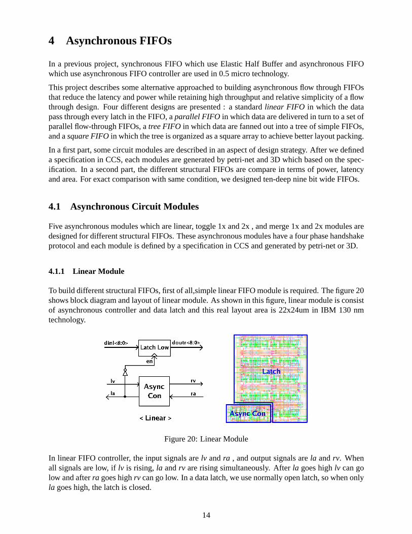
The router has three bidirectional ports and each port possesses one switch and one join modules.Thus, three switches and three joins are in one router. The area of one router is 73µm × 62 µm(4526µm2).
Figure 19: Layout of Async Router
13
4 Asynchronous FIFOs
In a previous project, synchronous FIFO which use Elastic Half Buffer and asynchronous FIFOwhich use asynchronous FIFO controller are used in 0.5 micro technology.
This project describes some alternative approached to building asynchronous flow through FIFOsthat reduce the latency and power while retaining high throughput and relative simplicity of a flowthrough design. Four different designs are presented : a standardlinear FIFO in which the datapass through every latch in the FIFO, aparallel FIFO in which data are delivered in turn to a set ofparallel flow-through FIFOs, atree FIFO in which data are fanned out into a tree of simple FIFOs,and asquare FIFOin which the tree is organized as a square array to achieve better layout packing.
In a first part, some circuit modules are described in an aspect of design strategy. After we defineda specification in CCS, each modules are generated by petri-net and 3D which based on the spec-ification. In a second part, the different structural FIFOs are compare in terms of power, latencyand area. For exact comparison with same condition, we designed ten-deep nine bit wide FIFOs.
4.1 Asynchronous Circuit Modules
Five asynchronous modules which are linear, toggle 1x and 2x , and merge 1x and 2x modules aredesigned for different structural FIFOs. These asynchronous modules have a four phase handshakeprotocol and each module is defined by a specification in CCS and generated by petri-net or 3D.
4.1.1 Linear Module
To build different structural FIFOs, first of all,simple linear FIFO module is required. The figure 20shows block diagram and layout of linear module. As shown in this figure, linear module is consistof asynchronous controller and data latch and this real layout area is 22x24um in IBM 130 nmtechnology.
Figure 20: Linear Module
In linear FIFO controller, the input signals arelv andra , and output signals arela andrv. Whenall signals are low, iflv is rising, la andrv are rising simultaneously. Afterla goes highlv can golow and afterra goes highrv can go low. In a data latch, we use normally open latch, so when onlyla goes high, the latch is closed.
14

A linear FIFO cell can be specified in CCS as follows:
L = lv ↑ c la ↑ lv ↓ la ↓ L
R= c rv ↑ ra ↑ rv ↓ ra ↓ R
FIFO= (L|R)/{c}
The eventc synchronizes the two processes, so as mentioned before,ra must go low andlv mustrise before both processes may proceed.
According to above CCS format, we can get petri-net and state transition graph from petrify. Fig-ure 21 shows petri-net and state transition graph
Figure 21: Linear Module’s Petri-net and STG
4.1.2 Toggle Module
In our system, two different operation toggle modules are required for different structural asyn-chronous FIFOs. The first toggle module’s operation called toggle-1x is that the data is sent up anddown but the second toggle module called toggle-2x operates that the data is sent up, down anddown again. The toggle-2x is only used in square FIFO which will be explained the next chapter.
The figure 22 shows block diagram and layout of toggle 1x and 2x module. As shown in this figure,the toggle module is similar with linear module and real layout areas are 20x35um (toggle-1x) and26x35um (toggle-2x).
Figure 22: Toggle Module
Toggle module’s operation is same with linear module’s. The important specification is that afterfinishing all transition with upper channel, lower channel’s transition can start. Since we use this
15

protocol, the normally open data latch can be used. In other words, ifla or rv0 didn’t go low, thenext transition couldn’t be started, so even though we use normally opened latch, the data can notbe overlapped.
A toggle FIFO cell can be specified in CCS as follows:
L = lv ↑ c1 x1 la ↑ lv ↓ la ↓ lv ↑ c2 x2 la ↑ lv ↓ la ↓ L
R1= c1 rv0 ↑ ra0 ↑ x1 rv0 ↓ ra0 ↓ R1
R2= c2 rv1 ↑ ra1 ↑ x2 rv1 ↓ ra1 ↓ R2
TOGGLE= (L|R1|R2)/{c1, c2, x1, x2}
The toggle’s CCS has more synchronizer such asc1,x1,c2,x2compared with linear FIFO. Typi-cally, if there are more synchronizer, the concurrency is more constrained. That means when thereare fewer concurrency, circuit can be expressed simpler than opposite case, but timing constraintis increased. A various trial in petrify and 3D, we found proper petri-net and state transition graphbetween relationship of concurrency and timing constraint.
According to above CCS format, three different type of transition graph is depicted in figure 23.
Figure 23: Toggle Petri-net and STG
In this figure, the first graph is specification of 3D, according to this state graph, toggle-1x issynthesized by 3D. The toggle-2x is synthesized by petrify. The reason for using different asyn-chronous circuit design tool to synthesize the circuit is that these tools generate different circuit ina same specification. In a some condition, 3D can generate simpler circuit than the petrify and viceversa. As a result, a toggle-1x is synthesized by 3D and toggle-2x is synthesized by petrify.
4.1.3 Merge Module
Two kinds of merge module is required for our asynchronous FIFOs. Merge module has two leftchannel and one right channel. This module receives two requests from left channel and sendonly one input channel at a time to right channel. This module didn’t receive the input channelarbitrarily. According to sequence, the merge modules are operated. Merge-1x module receive leftup channel and then left bottom channel. However, merge-2x module receive left up, down anddown again. This merge-2x module is only required in square FIFO which will be explained innext chapter.
16
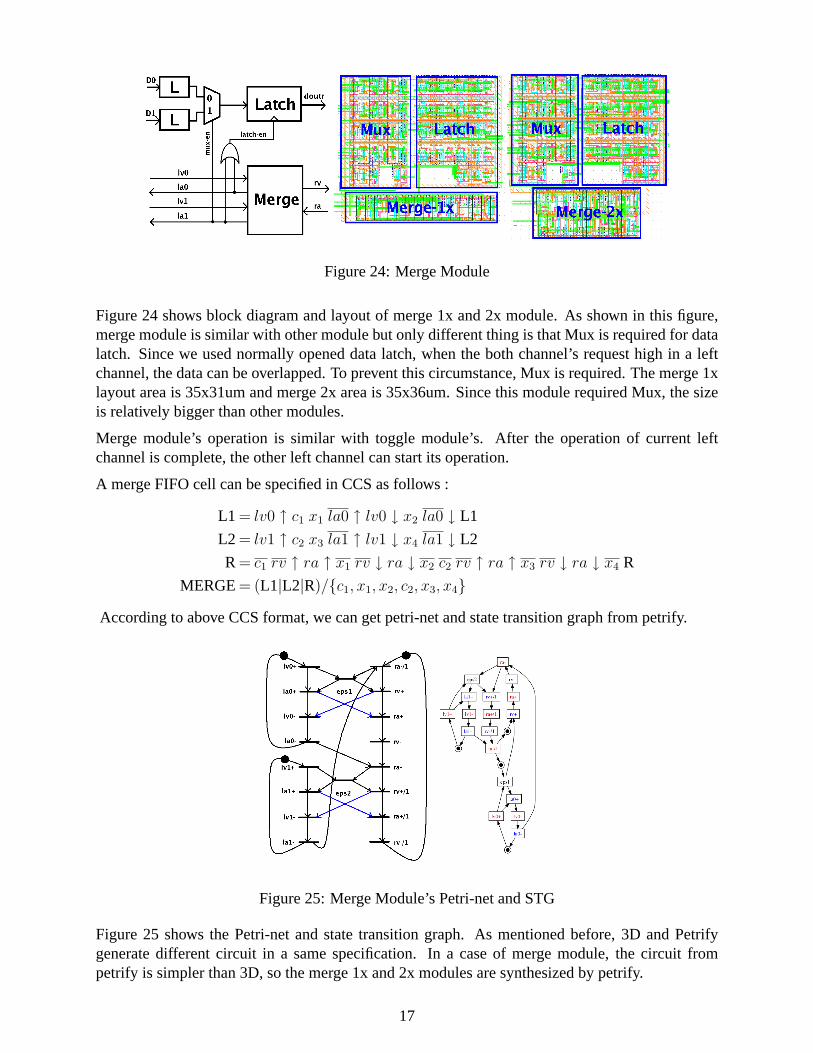
Figure 24: Merge Module
Figure 24 shows block diagram and layout of merge 1x and 2x module. As shown in this figure,merge module is similar with other module but only different thing is that Mux is required for datalatch. Since we used normally opened data latch, when the both channel’s request high in a leftchannel, the data can be overlapped. To prevent this circumstance, Mux is required. The merge 1xlayout area is 35x31um and merge 2x area is 35x36um. Since this module required Mux, the sizeis relatively bigger than other modules.
Merge module’s operation is similar with toggle module’s. After the operation of current leftchannel is complete, the other left channel can start its operation.
A merge FIFO cell can be specified in CCS as follows :
L1 = lv0 ↑ c1 x1 la0 ↑ lv0 ↓ x2 la0 ↓ L1
L2 = lv1 ↑ c2 x3 la1 ↑ lv1 ↓ x4 la1 ↓ L2
R= c1 rv ↑ ra ↑ x1 rv ↓ ra ↓ x2 c2 rv ↑ ra ↑ x3 rv ↓ ra ↓ x4 R
MERGE= (L1|L2|R)/{c1, x1, x2, c2, x3, x4}
According to above CCS format, we can get petri-net and state transition graph from petrify.
Figure 25: Merge Module’s Petri-net and STG
Figure 25 shows the Petri-net and state transition graph. As mentioned before, 3D and Petrifygenerate different circuit in a same specification. In a case of merge module, the circuit frompetrify is simpler than 3D, so the merge 1x and 2x modules are synthesized by petrify.
17
4.2 Different Structural FIFOs
In this project, we will compare different structural FIFOs for low latency and low power whileretaining high throughput. In this chapter, four different type FIFOs will be described, linear, par-allel, tree and square FIFOs. By combining above asynchronous circuit modules, we will comparea various FIFOs in ten-deep nine bit wide FIFOs in terms of latency, power and area.
4.2.1 Linear FIFO
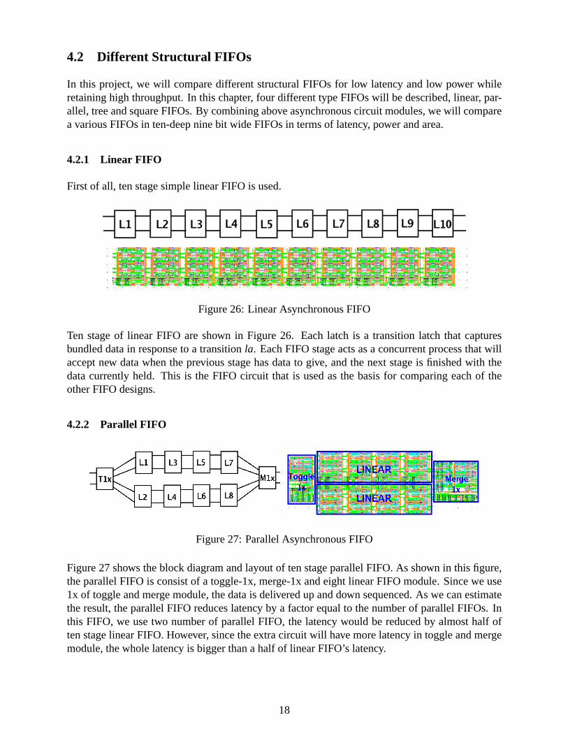
First of all, ten stage simple linear FIFO is used.
Figure 26: Linear Asynchronous FIFO
Ten stage of linear FIFO are shown in Figure 26. Each latch is a transition latch that capturesbundled data in response to a transitionla. Each FIFO stage acts as a concurrent process that willaccept new data when the previous stage has data to give, and the next stage is finished with thedata currently held. This is the FIFO circuit that is used as the basis for comparing each of theother FIFO designs.
4.2.2 Parallel FIFO
Figure 27: Parallel Asynchronous FIFO
Figure 27 shows the block diagram and layout of ten stage parallel FIFO. As shown in this figure,the parallel FIFO is consist of a toggle-1x, merge-1x and eight linear FIFO module. Since we use1x of toggle and merge module, the data is delivered up and down sequenced. As we can estimatethe result, the parallel FIFO reduces latency by a factor equal to the number of parallel FIFOs. Inthis FIFO, we use two number of parallel FIFO, the latency would be reduced by almost half often stage linear FIFO. However, since the extra circuit will have more latency in toggle and mergemodule, the whole latency is bigger than a half of linear FIFO’s latency.
18

Figure 28: Tree Asynchronous FIFO
4.2.3 Tree FIFO
Figure 28 shows the block diagram and layout of ten stage tree FIFO. The tree structural FIFO isconsist of three 1x toggle and merge modules and four linear modules. A tree FIFO is essentially aparallel FIFO but one in which each of the parallel FIFOs are also parallel. The data are fanned outto a binary tree of FIFO cells, and then collected in another binary tree to a single output cell. Themost important things in tree FIFO, the entire FIFO behaves exactly like a ten-deep FIFO, but datapass through only 5 stages. As a result, the latency would be the lowest among our four differentstructural FIFOs.
4.2.4 Square FIFO
Figure 29: Square Asynchronous FIFO
Figure 29 shows the block diagram and layout of ten stage square FIFO. Square FIFO can com-pensate the drawback of tree FIFO, which the physical tree structure may not pack well onto thetwo-dimensional surface of an IC since rectangular shapes might pack better in terms of layout.As shown in this figure, however, each module don’t have same size, so it is not exact rectangularshape.
In a square FIFO, data pattern is little bit different with other FIFOs. The first data goes all theway to the right end before dropping into the vertical FIFO in the middle. The second goes to
19
the second column and the next drops into the first column and the cycle repeats. So, toggle 2x isrequired in the first column and top row, and merge 2x is required in the third column and bottomrow. It can make the bottom row collects data from the vertical FIFOs in the same order using thesame idea. Even though tree’s latency is more efficient than square’s, the square arrangement maybe more amenable to planar VLSI layout than the tree.
4.3 Performance Comparison
In order to evaluate the performance of the various FIFO organizations presented here, we usedHspice simulation with extracting file from cadence. For precise evaluation, first of all, we com-pared each module’s power and size. Table 1 denotes the result of simulation.
Module Power (µW) % Power Increase Size (µm2) % SizeLinear 387.1 0 % 2x24 (528) 0 %Toggle 1x 467.8 20.8% 20x35 (700) 32.6%Toggle 2x 551.4 42.4% 26x35 (910) 72.3%Merge 1x 546.5 41.2% 35x31 (1085) 105.5%Merge 2x 615.8 59.1% 35x36 (1260) 138.6%
Table 1: Each Module Power and Size
The percent power and size is a measure of how much the value of each FIFO modules higher thana simple linear FIFO. In this table, we didn’t compare the latency because toggle and merge 2x isnot symmetric circuit, so the latency of (lv0, lv1) and (rv0, rv1) is different. As we can see in thistable, merge module’s power and size is relatively bigger than others because of Mux. This sizeincludes the data latch and asynchronous FIFO controller. Actually, the data latch’s size occupiedmore than 70% of whole FIFO.
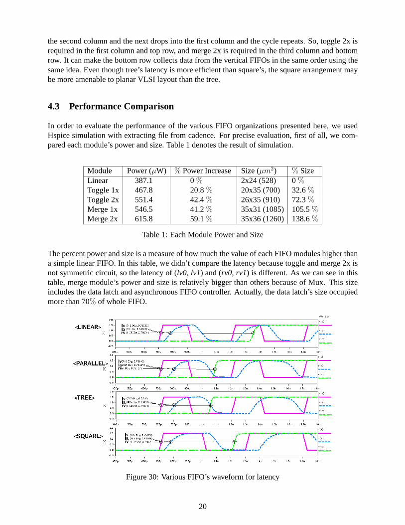
Figure 30: Various FIFO’s waveform for latency
20
By combining of each module, we designed various FIFOs, linear, parallel, tree and square FIFOs.Figure 30 shows the simulation result in Hspice. In this figure, signallv, la is first stage’s inputand output, and signalrv is last stage’s output. To measure the latency of various FIFO, we needto know when request signallv comes into first stage, how long take the time signalrv goes up. Asshown in this figure, parallel and tree FIFO’s latency is very low. Even though the parallel and treealso have ten stage, when the FIFOs are empty, the data is through only 5 or 6 stage.
Latency (ps) % Latency power (mW) % Power size (µm2) % SizeLinear 640 100% 2.459 100% 5280 0 %Parallel 375 58.6% 1.679 68.3% 6010 13.8%Tree 330 51.6% 1.479 60.1% 7470 41.4%Square 510 79.7% 1.546 62.9% 7123 34.9%
Table 2: Latency, Power and Size
The various FIFOs latency, power and area is summarized in Table 2. This table illustrates treeFIFO has the lowest latency and power, but drawback is size. The square FIFO has not low latency.An aspects of shape, however, the square FIFO’s shape is almost rectangular. Even though the areais relatively big among a various FIFO, it has minimum length in its longest dimension(verticaland horizontal).
In our test-bench, we simulate these various FIFO to compare the efficiency with synchronousFIFO. However, since asynchronous FIFO is much faster than synchronous FIFO, it is hard todistinguish the latency among various asynchronous FIFO. The whole test-bench is used for mea-suring throughput and we get a result that each FIFO’s throughput is almost same. Therefore, aswe expected, we designed low latency asynchronous FIFO while retaining high throughput.
4.4 Conclusion
This project has explored some circuit for building various asynchronous FIFO that have lowerlatency than a simple linear FIFO. To reduce latency and power consumption, fewer signal transi-tions are needed to pass data through the FIFO.
The linear FIFO uses a distribution to compare with other various FIFO, so we use simple linearFIFO which from Dr. Stevens linear FIFO. The parallel shows that the latency is reduced by afactor equal to the number of parallel FIFOs the data are distributed into. If we designed three waytoggle in front of parallel FIFO, the latency might be reduced by one third. Tree FIFO distributesthe data into a binary tree of FIFOs. Even though the layout shape is not rectangular, this has thelowest latency and power consumption. Square FIFO is similar with tree FIFO, but there are bigdifference. Data are stored in the top and bottom FIFOs as those cells are doing the distribution.In addition, the shape is fit well in terms of VLSI layout.
In our SoC design, we don’t need many stage FIFO. In a previous project, we only use 2 stageFIFO, but to compare various FIFO in a same condition, we use ten stage FIFOs. According totraffic signal from PE, if we need from 4 to 8 stage FIFO, the parallel FIFO would be efficient dueto low latency and low power consumption.
21
5 Behavioral Validation & Results
5.1 Golden Model & Testbench
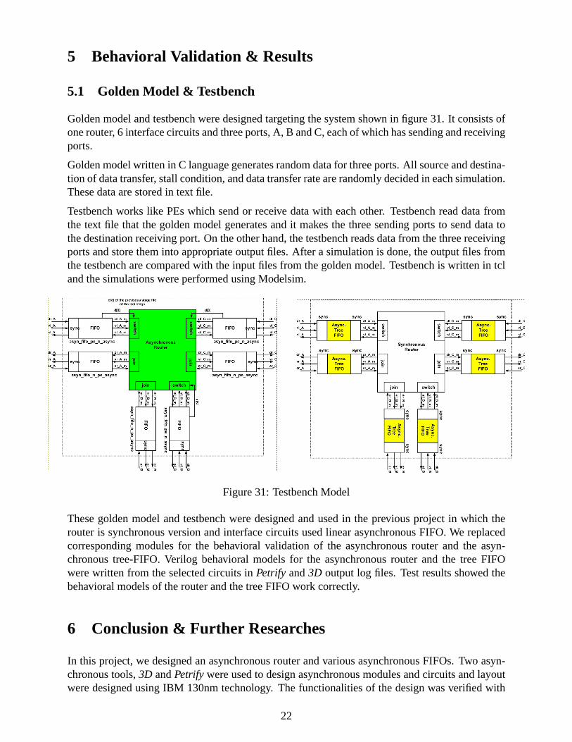
Golden model and testbench were designed targeting the system shown in figure 31. It consists ofone router, 6 interface circuits and three ports, A, B and C, each of which has sending and receivingports.
Golden model written in C language generates random data for three ports. All source and destina-tion of data transfer, stall condition, and data transfer rate are randomly decided in each simulation.These data are stored in text file.
Testbench works like PEs which send or receive data with each other. Testbench read data fromthe text file that the golden model generates and it makes the three sending ports to send data tothe destination receiving port. On the other hand, the testbench reads data from the three receivingports and store them into appropriate output files. After a simulation is done, the output files fromthe testbench are compared with the input files from the golden model. Testbench is written in tcland the simulations were performed using Modelsim.
Figure 31: Testbench Model
These golden model and testbench were designed and used in the previous project in which therouter is synchronous version and interface circuits used linear asynchronous FIFO. We replacedcorresponding modules for the behavioral validation of the asynchronous router and the asyn-chronous tree-FIFO. Verilog behavioral models for the asynchronous router and the tree FIFOwere written from the selected circuits inPetrify and3D output log files. Test results showed thebehavioral models of the router and the tree FIFO work correctly.
6 Conclusion & Further Researches
In this project, we designed an asynchronous router and various asynchronous FIFOs. Two asyn-chronous tools,3D andPetrify were used to design asynchronous modules and circuits and layoutwere designed using IBM 130nm technology. The functionalities of the design was verified with
22

verilog behavioral model and ModelSim simulation. The timing analysis of operation of circuitswere performed in HSPICE simulation.
The asynchronous router is a main module composing asynchronous network fabric to interconnectprocessing elements or IP blocks in SoC system. As one of following researches of this project,the operation and performance of the asynchronous router need to be verified and evaluated withother modules, Processing Elements and interface circuits, which are not currently available in130nm technology. Comparison of this asynchronous router with the synchronous version fromthe previous project may be another valuable research.
Various asynchronous FIFOs, such as linear, tree, parallel, and square FIFO were designed andanalyzed as well. As an aspects of latency, power consumption, and area, we compared variousFIFO with simple linear FIFO. By combining linear, toggle 1x and 2x , and merge 1x and 2x, wedesigned various FIFOs. As a result, tree FIFO has the lowest latency and power consumption, butit occupied relatively big area. Therefore, in our SoC system, the parallel FIFO is more efficientthan others since it has lower latency and power consumption and the size increases only 10% withsimple linear FIFO. However, to use the most appropriate FIFO in an interface system, it dependson which part is more weighted than others, such as latency and power consumption. In furtherresearch, we need to design more simple circuit by reducing concurrency and investigate moreefficient FIFOs for instance three way parallel FIFO or folded FIFO.
Our system will be fabricated in both 130nm and 0.5µm in near future. For fabricating our asyn-chronous interconnect network system, the rest of modules such as PE and synchronizers are sup-posed to be designed in 130nm technology which can be possible only after synthesis and APRprocess are available in 130nm technology. And, only the asynchronous router is required to beredesigned for 0.5µm chip
23
References
[1] T. Bjerregaard and S. Mahadevan.A survey of research and practices of network-on-chip.ACM Computing Surveys, 38(1), 2006.
[2] Amde, M., Felicijan, T., Edwards, A. E. D., and Lavagno, L.Asynchronous on-chip networks.IEE Proceedings of Computers and Digital Techniques 152, 273-283, 2005
[3] R. Milner. Communication and Concurrency. Prentice-Hall, London, 1989
[4] Kenneth S. Stevens, Ran Ginosar, and Shai RotemRelative Timing. IEEE Transactions onVery Large Scale Integration (VLSI) Systems, 11(1), Feb. 2003, pp. 129-140.
[5] Erik BrunvandLow Latency Self-Timed Flow Through FIFOs. 16th Conference on AdvancedResearch in VLSI, Chapel Hill, NC, March 1995.
24
A Petrify Input Files
.
A.1 Asynchronous Network Fabric Modules
A.1.1 Switch.g
25
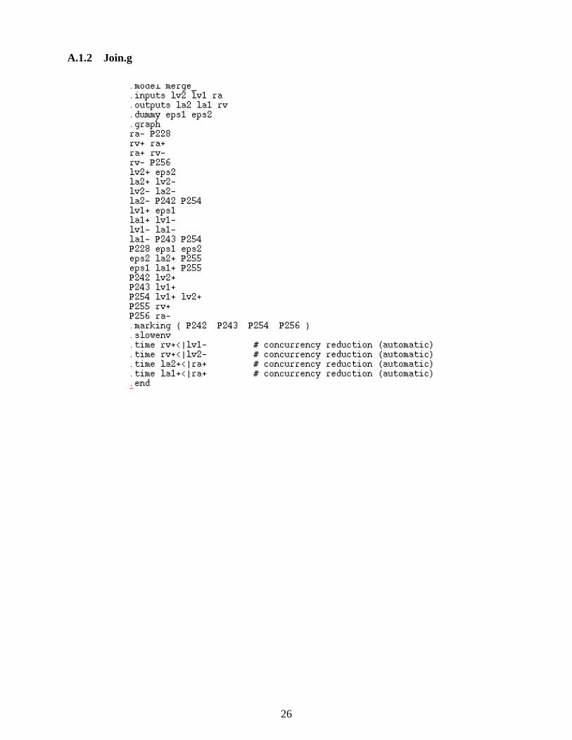
A.1.2 Join.g
26