asynchronous ic interconnect network design and ...stevew/papers/pdf/iccd2005.pdfasynchronous ic...
TRANSCRIPT

Asynchronous IC Interconnect Network Design and Implementation Using aStandard ASIC Flow
Bradley R. QuintonDept. of Electrical and Computer
EngineeringUniversity of British Columbia
Mark R. GreenstreetDept. of Computer Science
University of British [email protected]
Steven J.E. WiltonDept. of Electrical and Computer
EngineeringUniversity of British Columbia
Abstract
The implementation of interconnect is becoming asignificant challenge in modern IC design. Bothsynchronous and asynchronous strategies have beensuggested to manage this problem. Creating a low skewclock tree for synchronous inter-block pipeline stages isa significant challenge. Asynchronous interconnectdoes not require a global clock and therefore it has apotential advantage in terms of design effort. Thispaper presents an asynchronous interconnect designthat can be implemented using a standard ASIC flow.This design is considered in the context of a simpleinterconnect network. The results demonstrate thatthere is a region of the design space where theimplementation provides an advantage over asynchronous interconnect. A detailed comparison ofpower, area and latency of the two strategies is alsoprovided for a range of IC scenarios.
1. Introduction
The implementation of interconnect is becoming asignificant issue in modern IC design. In olderprocesses, wire delays were not significant whencompared to gate delays. This greatly simplified inter-block communication since any part of the IC couldcommunicate with any other part without special timingconsiderations. However, in modern processes, wiredelays are significant, and inter-block communication isno longer a simple matter [1]. Without careful design,interconnect may become the critical path on a given ICand limit the overall operation. Repeater insertion hasbeen employed to decrease wire latency and improveperformance [2]. However, even optimally placedbuffers may not be sufficient and register pipelining isrequired in some situations [3]. Although registerpipelining increases throughput, there is a significantdesign effort required to implement these synchronouspipeline stages since each individual register requires alow-skew clock. Asynchronous techniques have beensuggested as a potential solution to the problem of IC
interconnect [4,5]. These asynchronous techniques donot require a global clock. Instead, a localrequest/acknowledgement protocol is used to co-ordinated each data transfer.
Although a number of asynchronous protocols andimplementations have been explored with the intentionof being used for IC interconnect, theseimplementations require custom designed circuits anduser-implemented CAD tools or manual designoptimization. These techniques are not feasible fortypical ASIC/SoC designs that are implemented withstandard cells and commercial CAD tools (oftenreferred to as a standard ASIC flow). In this paper wepresent an asynchronous interconnect design that can beimplemented using only standard cells and optimizedusing commercially available CAD tools. We explorethis design in the context of a simple interconnectnetwork. We show that while the requirements of anASIC design flow impose limitations on theperformance of the asynchronous interconnect there isstill a significant portion of the overall design spacewhere an asynchronous interconnect provides anadvantage over a synchronous interconnect. In addition,we compare the area, power and latency of synchronousand asynchronous implementations of an interconnectnetwork for a range of IC sizes and constructions.These results are based on a standard ASIC flow and areextracted from silicon-ready placed and routed designs.Finally, we conclude by identifying some relativelysimple changes to the standard ASIC flow that couldsignificantly increase the performance and reduce thecost of the asynchronous interconnect.
2. Related work
The problem of managing high-speed interconnecthas been addressed in a number of ways. Forsynchronous interconnects, a number of algorithms havebeen developed which determine the optimal repeaterand register insertion locations [3,6]. While thesealgorithms determine the optimal location of registers to
pipeline the interconnect and achieve a target clockfrequency, they do not address the issues of producing alow-skew clock for each of these registers. High-speedclock tree design remains a significant challenge.
Other research has focused on asynchronousinterconnect techniques. These techniques can beclassified into two broad categories: 1) bundled-dataand 2) delay-insensitive [7]. Bundled-data designsmanage a number of bits together, and make use ofrequest/acknowledge signalling which is separate fromthe data. Because of this separation, these designsrequire delay-matching between the data bits and thecontrol signalling. In contrast, delay-insensitive designsrely on a data encoding that allows the controlsignalling to be extracted from the encoded data. Thisencoding removes the requirement of delay-matchingfrom these designs. While bundled-data techniques tendto be more efficient and higher performance than delay-insensitive techniques, the requirement of delay-matching is not compatible with current commercialCAD tools. Therefore bundled-data techniques werenot considered for this work. There are a number ofdifferent delay-insensitive designs. These designsprimarily differ on the basis of data encoding methodsand handshaking protocols. There are many possibledata encodings [8], however most research has focusedon two of these encodings: 1) dual-rail and 2) 1-of-4.Dual-rail uses a two bit encoding for each data bit,whereas 1-of-4 encoding uses a four-bit code for eachtwo data bits. There are two widely used handshakingprotocols: 2-phase and 4-phase. When using 2-phasehandshaking the transitions of the control andacknowledgement signals indicate the completion of atransfer. When using 4-phase handshaking the value ofthe control signals indicate the completion of a transfer.The commercially available Nexus crossbar fromFulcrum Microsystems uses a 1-of-4, 4-phaseimplementation [5]. Unlike our work the Nexuscrossbar is based on custom designed pre-chargedomino logic. Work by Bainbridge and Furber has alsobeen based on a 1-of-4, 4-phase approach [4]. Again,unlike our work their work requires a sequential cellthat does not exist in normal standard cell libraries (a C-element) and does not make use of circuit optimizationfrom commercial CAD tools. A dual-rail, 2-phaseprotocol, LEDR, has been described [9]. However thisimplementation was described in terms of customdynamic logic, and was not investigated in the contextof interconnect with long wires. Finally, Stevens hascompared a number of synchronous and asynchronousinterconnect implementations using first order models[10]. These first order models do not consider theperformance or cost in the context of a standard ASICflow.
3. Interconnect network structure
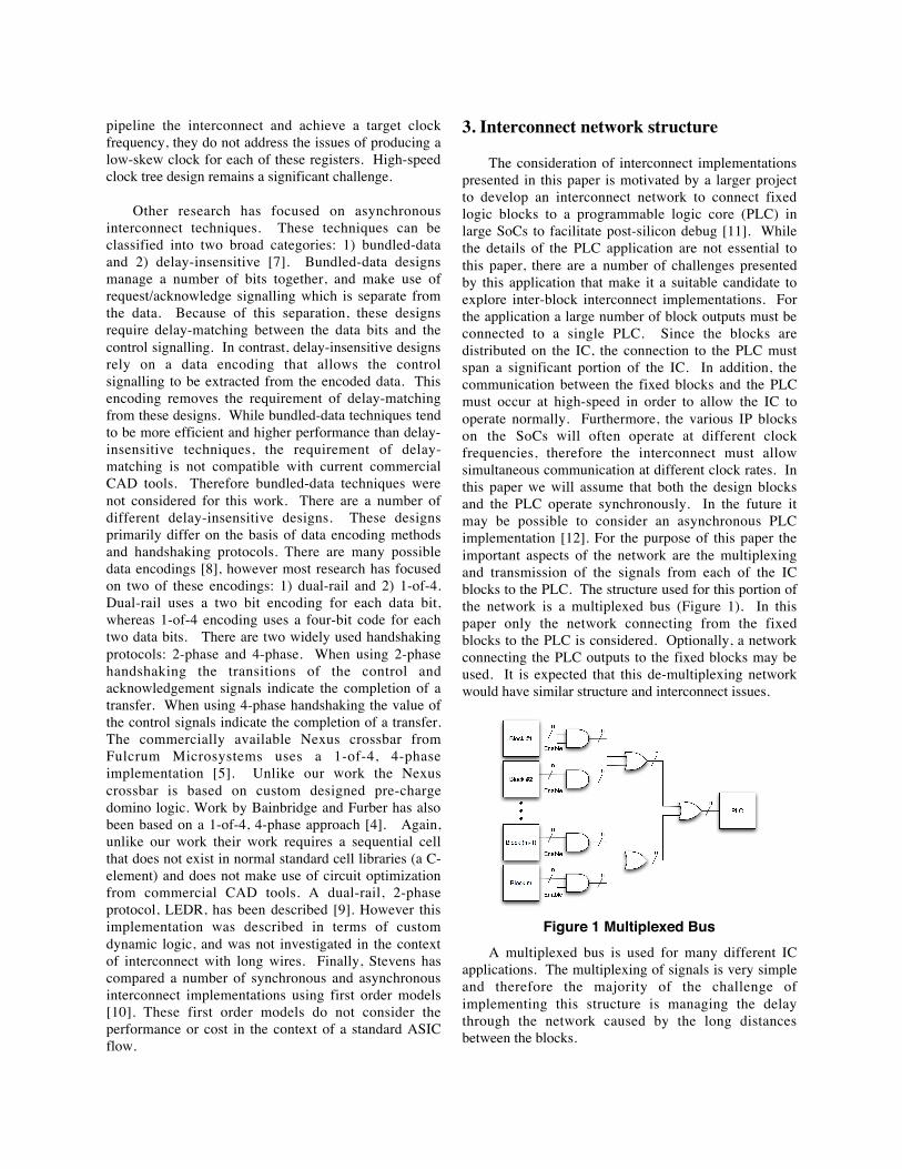
The consideration of interconnect implementationspresented in this paper is motivated by a larger projectto develop an interconnect network to connect fixedlogic blocks to a programmable logic core (PLC) inlarge SoCs to facilitate post-silicon debug [11]. Whilethe details of the PLC application are not essential tothis paper, there are a number of challenges presentedby this application that make it a suitable candidate toexplore inter-block interconnect implementations. Forthe application a large number of block outputs must beconnected to a single PLC. Since the blocks aredistributed on the IC, the connection to the PLC mustspan a significant portion of the IC. In addition, thecommunication between the fixed blocks and the PLCmust occur at high-speed in order to allow the IC tooperate normally. Furthermore, the various IP blockson the SoCs will often operate at different clockfrequencies, therefore the interconnect must allowsimultaneous communication at different clock rates. Inthis paper we will assume that both the design blocksand the PLC operate synchronously. In the future itmay be possible to consider an asynchronous PLCimplementation [12]. For the purpose of this paper theimportant aspects of the network are the multiplexingand transmission of the signals from each of the ICblocks to the PLC. The structure used for this portion ofthe network is a multiplexed bus (Figure 1). In thispaper only the network connecting from the fixedblocks to the PLC is considered. Optionally, a networkconnecting the PLC outputs to the fixed blocks may beused. It is expected that this de-multiplexing networkwould have similar structure and interconnect issues.
Figure 1 Multiplexed BusA multiplexed bus is used for many different IC
applications. The multiplexing of signals is very simpleand therefore the majority of the challenge ofimplementing this structure is managing the delaythrough the network caused by the long distancesbetween the blocks.
4. Experimental framework
4.1 Target ICs
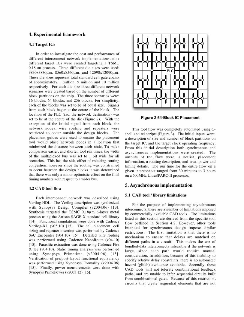
In order to investigate the cost and performance ofdifferent interconnect network implementations, ninedifferent target ICs were created targeting a TSMC0.18µm process. Three different die sizes were used:3830x3830µm, 8560x8560µm, and 12090x12090µm.These die sizes represent total standard cell gate countsof approximately 1 million, 5 million and 10 millionrespectively. For each die size three different networkscenarios were created based on the number of differentblock partitions on the chip. The three scenarios were:16 blocks, 64 blocks, and 256 blocks. For simplicity,each of the blocks was set to be of equal size. Signalsfrom each block began at the centre of the block. Thelocation of the PLC (i.e., the network destination) wasset to be at the centre of the die (Figure 2). With theexception of the initial signal from each block, thenetwork nodes, wire routing and repeaters wererestricted to occur outside the design blocks. Theplacement guides were used to ensure the placementtool would place network nodes in a location thatminimized the distance between each node. To makecomparison easier, and shorten tool run times, the widthof the multiplexed bus was set to 1 bit wide for allscenarios. This has the side effect of reducing routingcongestion, however since the routing was constrainedto occur between the design blocks it was determinedthat there was only a minor optimistic effect on the finaltiming numbers with respect to a wider bus.
4.2 CAD tool flow
Each interconnect network was described usingVerilog-HDL. The Verilog description was synthesizedwith Synopsys Design Compiler (v2004.06) [13].Synthesis targeted the TSMC 0.18µm 6-layer metalprocess using the Artisan SAGE-X standard cell library[14]. Functional simulations were done with CadenceVerilog-XL (v05.10) [15]. The cell placement, cellsizing and repeater insertion was performed by CadenceSoC Encounter (v04.10) [15]. Detailed wire routingwas performed using Cadence NanoRoute (v04.10)[15]. Parasitic extraction was done using Cadence Fire& Ice (v04.10). Static timing analysis was performedusing Synopsys Primetime (v2004.06) [15].Verification of pre/post-layout functional equivalencywas performed using Synopsys Formality (v2004.06)[15]. Finally, power measurements were done withSynopsys PrimePower (v2003.12) [15].
Figure 2 64-Block IC Placement
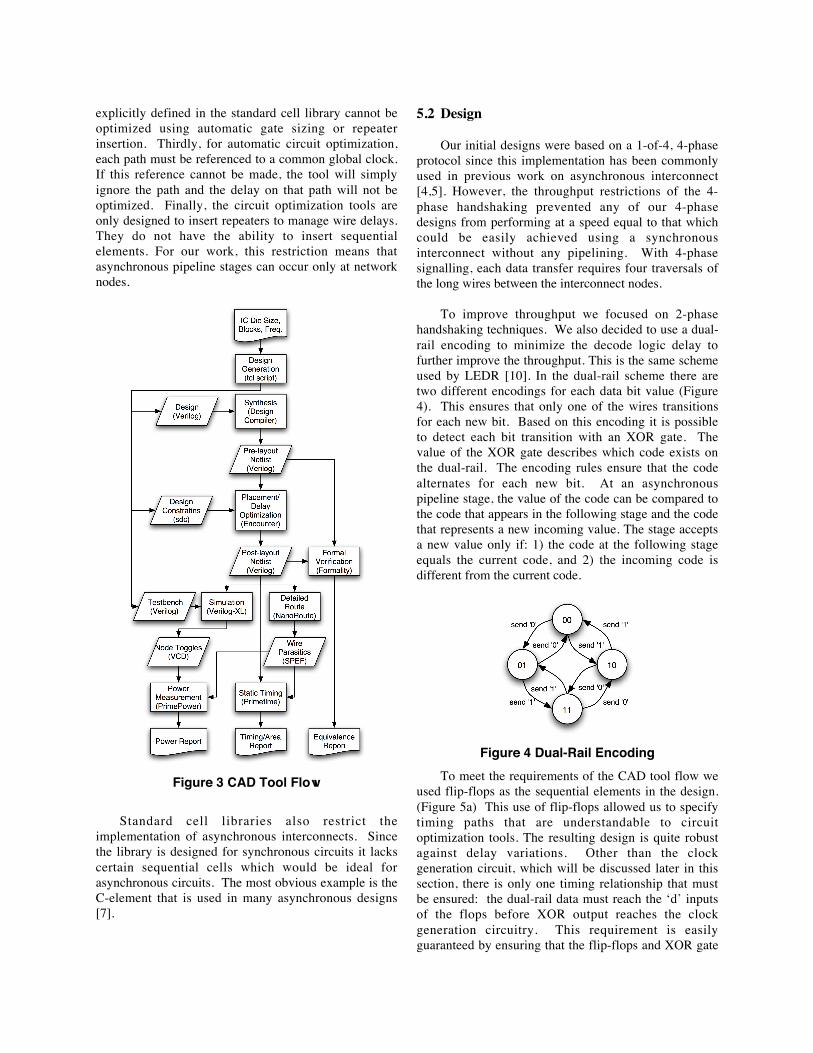
This tool flow was completely automated using C-shell and tcl scripts (Figure 3). The initial inputs were:a description of size and number of block partitions onthe target IC, and the target clock operating frequency.From this initial description both synchronous andasynchronous implementations were created. Theoutputs of the flow were: a netlist, placementinformation, a routing description, and area, power andtiming details. The run time for the entire flow on agiven interconnect ranged from 30 minutes to 3 hourson a 500MHz UltraSPARC-II processor.
5. Asynchronous implementation
5.1 CAD tool / library limitations
For the purpose of implementing asynchronousinterconnects, there are a number of limitations imposedby commercially available CAD tools. The limitationslisted in this section are derived from the specific toolflow outlined in Section 4.2. However, other toolsintended for synchronous design impose similarrestrictions. The first limitation is that there is nomechanism to ensure that delays are matched ondifferent paths in a circuit. This makes the use ofbundled-data interconnects infeasible if the network islarge, since each path would require manualconsideration. In addition, because of this inability tospecify relative delay constraints, there is no automatedhazard (glitch) avoidance available. Secondly, theseCAD tools will not tolerate combinational feedbackpaths, and are unable to infer sequential circuits builtfrom combinational gates. Because of this restriction,circuits that create sequential elements that are not
explicitly defined in the standard cell library cannot beoptimized using automatic gate sizing or repeaterinsertion. Thirdly, for automatic circuit optimization,each path must be referenced to a common global clock.If this reference cannot be made, the tool will simplyignore the path and the delay on that path will not beoptimized. Finally, the circuit optimization tools areonly designed to insert repeaters to manage wire delays.They do not have the ability to insert sequentialelements. For our work, this restriction means thatasynchronous pipeline stages can occur only at networknodes.
Figure 3 CAD Tool Flow
Standard cell libraries also restrict theimplementation of asynchronous interconnects. Sincethe library is designed for synchronous circuits it lackscertain sequential cells which would be ideal forasynchronous circuits. The most obvious example is theC-element that is used in many asynchronous designs[7].
5.2 Design
Our initial designs were based on a 1-of-4, 4-phaseprotocol since this implementation has been commonlyused in previous work on asynchronous interconnect[4,5]. However, the throughput restrictions of the 4-phase handshaking prevented any of our 4-phasedesigns from performing at a speed equal to that whichcould be easily achieved using a synchronousinterconnect without any pipelining. With 4-phasesignalling, each data transfer requires four traversals ofthe long wires between the interconnect nodes.
To improve throughput we focused on 2-phasehandshaking techniques. We also decided to use a dual-rail encoding to minimize the decode logic delay tofurther improve the throughput. This is the same schemeused by LEDR [10]. In the dual-rail scheme there aretwo different encodings for each data bit value (Figure4). This ensures that only one of the wires transitionsfor each new bit. Based on this encoding it is possibleto detect each bit transition with an XOR gate. Thevalue of the XOR gate describes which code exists onthe dual-rail. The encoding rules ensure that the codealternates for each new bit. At an asynchronouspipeline stage, the value of the code can be compared tothe code that appears in the following stage and the codethat represents a new incoming value. The stage acceptsa new value only if: 1) the code at the following stageequals the current code, and 2) the incoming code isdifferent from the current code.
Figure 4 Dual-Rail EncodingTo meet the requirements of the CAD tool flow we
used flip-flops as the sequential elements in the design.(Figure 5a) This use of flip-flops allowed us to specifytiming paths that are understandable to circuitoptimization tools. The resulting design is quite robustagainst delay variations. Other than the clockgeneration circuit, which will be discussed later in thissection, there is only one timing relationship that mustbe ensured: the dual-rail data must reach the ‘d’ inputsof the flops before XOR output reaches the clockgeneration circuitry. This requirement is easilyguaranteed by ensuring that the flip-flops and XOR gate
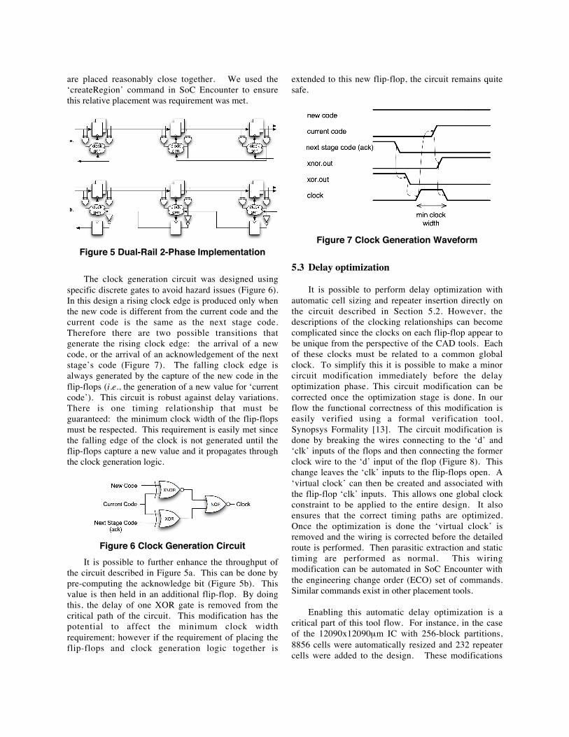
are placed reasonably close together. We used the‘createRegion’ command in SoC Encounter to ensurethis relative placement was requirement was met.
Figure 5 Dual-Rail 2-Phase Implementation
The clock generation circuit was designed usingspecific discrete gates to avoid hazard issues (Figure 6).In this design a rising clock edge is produced only whenthe new code is different from the current code and thecurrent code is the same as the next stage code.Therefore there are two possible transitions thatgenerate the rising clock edge: the arrival of a newcode, or the arrival of an acknowledgement of the nextstage’s code (Figure 7). The falling clock edge isalways generated by the capture of the new code in theflip-flops (i.e., the generation of a new value for ‘currentcode’). This circuit is robust against delay variations.There is one timing relationship that must beguaranteed: the minimum clock width of the flip-flopsmust be respected. This requirement is easily met sincethe falling edge of the clock is not generated until theflip-flops capture a new value and it propagates throughthe clock generation logic.
Figure 6 Clock Generation CircuitIt is possible to further enhance the throughput of
the circuit described in Figure 5a. This can be done bypre-computing the acknowledge bit (Figure 5b). Thisvalue is then held in an additional flip-flop. By doingthis, the delay of one XOR gate is removed from thecritical path of the circuit. This modification has thepotential to affect the minimum clock widthrequirement; however if the requirement of placing theflip-flops and clock generation logic together is
extended to this new flip-flop, the circuit remains quitesafe.
Figure 7 Clock Generation Waveform
5.3 Delay optimization
It is possible to perform delay optimization withautomatic cell sizing and repeater insertion directly onthe circuit described in Section 5.2. However, thedescriptions of the clocking relationships can becomecomplicated since the clocks on each flip-flop appear tobe unique from the perspective of the CAD tools. Eachof these clocks must be related to a common globalclock. To simplify this it is possible to make a minorcircuit modification immediately before the delayoptimization phase. This circuit modification can becorrected once the optimization stage is done. In ourflow the functional correctness of this modification iseasily verified using a formal verification tool,Synopsys Formality [13]. The circuit modification isdone by breaking the wires connecting to the ‘d’ and‘clk’ inputs of the flops and then connecting the formerclock wire to the ‘d’ input of the flop (Figure 8). Thischange leaves the ‘clk’ inputs to the flip-flops open. A‘virtual clock’ can then be created and associated withthe flip-flop ‘clk’ inputs. This allows one global clockconstraint to be applied to the entire design. It alsoensures that the correct timing paths are optimized.Once the optimization is done the ‘virtual clock’ isremoved and the wiring is corrected before the detailedroute is performed. Then parasitic extraction and statictiming are performed as normal. This wiringmodification can be automated in SoC Encounter withthe engineering change order (ECO) set of commands.Similar commands exist in other placement tools.
Enabling this automatic delay optimization is acritical part of this tool flow. For instance, in the caseof the 12090x12090µm IC with 256-block partitions,8856 cells were automatically resized and 232 repeatercells were added to the design. These modifications
improved the loop time by 12.46 ns thereby improvingthroughput by approximately 260 MHz. This largechange highlights the importance of allowing placementaware delay optimization when using a standard cellbased interconnects.
Figure 8 Circuit Modification
6. Synchronous implementation
6.1 CAD tool / library limitations
The CAD tool flow and standard cell library wereintended for synchronous design, therefore there werefewer limitations with respect to implementing thesynchronous interconnect. The one significantlimitation for this work was that current CAD tools donot support automatic insertion of sequential elementsto optimize wire delays. This ability does exist inalgorithms described research papers [3] but has not yetbeen implemented in the tools that we used for thiswork. Because of this, synchronous pipeline stageswere restricted to occurring only at network nodes.
6.2 Design
The synchronous design was implemented in abasic manner. Pipeline flops were restricted to thenetwork nodes. Circuits were designed to tolerate aclock skew of 100 ps. In addition a clock uncertaintymargin of 100 ps was assumed for all synchronoustiming measurements to compensate for jitter and othernon-ideal clock tree effects.
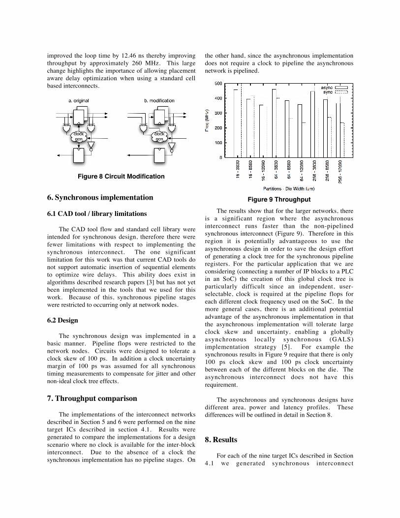
7. Throughput comparison
The implementations of the interconnect networksdescribed in Section 5 and 6 were performed on the ninetarget ICs described in section 4.1. Results weregenerated to compare the implementations for a designscenario where no clock is available for the inter-blockinterconnect. Due to the absence of a clock thesynchronous implementation has no pipeline stages. On
the other hand, since the asynchronous implementationdoes not require a clock to pipeline the asynchronousnetwork is pipelined.
Figure 9 ThroughputThe results show that for the larger networks, there
is a significant region where the asynchronousinterconnect runs faster than the non-pipelinedsynchronous interconnect (Figure 9). Therefore in thisregion it is potentially advantageous to use theasynchronous design in order to save the design effortof generating a clock tree for the synchronous pipelineregisters. For the particular application that we areconsidering (connecting a number of IP blocks to a PLCin an SoC) the creation of this global clock tree isparticularly difficult since an independent, user-selectable, clock is required at the pipeline flops foreach different clock frequency used on the SoC. In themore general cases, there is an additional potentialadvantage of the asynchronous implementation in thatthe asynchronous implementation will tolerate largeclock skew and uncertainty, enabling a globallyasynchronous locally synchronous (GALS)implementation strategy [5]. For example thesynchronous results in Figure 9 require that there is only100 ps clock skew and 100 ps clock uncertaintybetween each of the different blocks on the die. Theasynchronous interconnect does not have thisrequirement.
The asynchronous and synchronous designs havedifferent area, power and latency profiles. Thesedifferences will be outlined in detail in Section 8.
8. Results
For each of the nine target ICs described in Section4.1 we generated synchronous interconnect

implementations targeting 200 MHz, 350 MHz, 500MHz, and 750 MHz operation. We also createdasynchronous implementations targeting 200 MHz, 350MHz, and 500 MHz operation. For each case theminimum number of pipeline stages was used to meetthe target clock frequency. The area, power and latencywere determined for each implementation. These valueswere generated using detailed placed and routeddesigns. The worst-case library was used for allmeasurement. The worst-case library represents theslowest process corners with a 1.62V supply and dietemperature 125°C. Therefore no manufactured deviceswould be expected to have timing slower than thesevalues. For simplicity the worst-case library valueswere also used for power measurements. This allowsfor a consistent comparison between the two approachesbut does not represent the upper bound of the powerconsumption.
Due to space constraints, only results for the 350MHz target are presented for each IC scenario. This is arepresentative case highlighting the part of the designspace where the trade off between using anasynchronous implementation and building clock treefor inter-block pipeline stages occurs for many of thescenarios. The results for area, latency and power arepresented below.
The area of both implementations was comparedfor each of the nine design scenarios (Figure 10). Thearea reflects the total standard cell area and does notinclude the wire area. For the synchronous case the arearequired for a global clock tree was not included. Ingeneral the area for the asynchronous case is about eighttimes larger than the synchronous case. Althoughrelative area difference is quite large, in the context ofthe overall IC the difference is not that significant. Forexample the extra area of the asynchronous interconnectfor an 8560x8560µm IC with 64 block partitions isapproximately 0.09% per bit.
The latency of both implementations was comparedfor each of the nine design scenarios (Figure 11). Thelatency of the asynchronous interconnect is significantlylarger than the synchronous case. This latency is adirect result of the delay of the clock generation circuitand the ‘clk-q’ delay of the flip-flops. We anticipatethat the latency could be significantly reduced by addinga small number of cells to the standard cell library. Thisis discussed as future work in Section 9. Alternatively,there have been proposals for latency-insensitive designtechniques [16].
Figure 10 AreaThe power consumption of both implementations
was compared for each of the nine design scenarios(Figure 12). The results were generated by measuringthe power consumption while transmitting a fixed set of1000 random bits from a single input to the output. Toallow for consistent comparisons the results aredisplayed as the energy per end-to-end transfer. For thesynchronous case the power does not include the clocktree distribution power, but does include the powerconsumed by clocking each individual flip-flop. It isinteresting to note that the power of asynchronous caseis lower that the synchronous case for some of the largerscenarios. The difference is a result of the fact that inthe synchronous case each flip-flop in the designconsumes power on each clock cycle. In contrast forthe asynchronous case only the flip-flops on the activepath consume power.
Figure 11 Latency
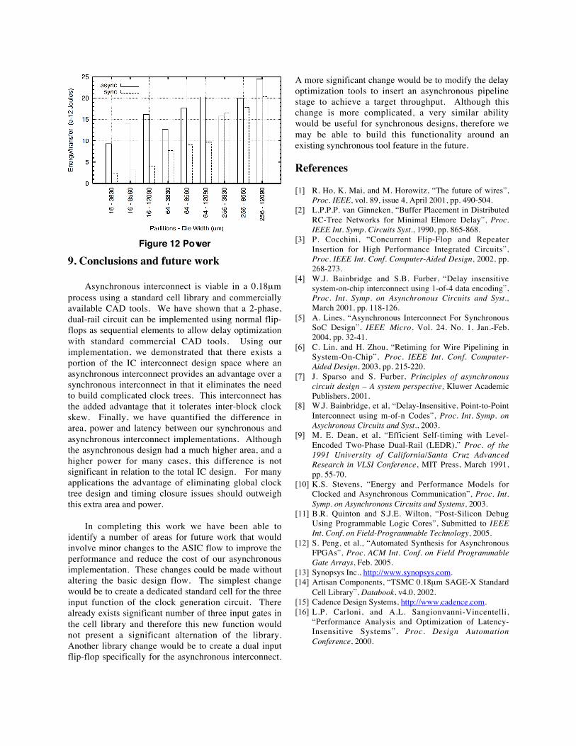
Figure 12 Power
9. Conclusions and future work
Asynchronous interconnect is viable in a 0.18µmprocess using a standard cell library and commerciallyavailable CAD tools. We have shown that a 2-phase,dual-rail circuit can be implemented using normal flip-flops as sequential elements to allow delay optimizationwith standard commercial CAD tools. Using ourimplementation, we demonstrated that there exists aportion of the IC interconnect design space where anasynchronous interconnect provides an advantage over asynchronous interconnect in that it eliminates the needto build complicated clock trees. This interconnect hasthe added advantage that it tolerates inter-block clockskew. Finally, we have quantified the difference inarea, power and latency between our synchronous andasynchronous interconnect implementations. Althoughthe asynchronous design had a much higher area, and ahigher power for many cases, this difference is notsignificant in relation to the total IC design. For manyapplications the advantage of eliminating global clocktree design and timing closure issues should outweighthis extra area and power.
In completing this work we have been able toidentify a number of areas for future work that wouldinvolve minor changes to the ASIC flow to improve theperformance and reduce the cost of our asynchronousimplementation. These changes could be made withoutaltering the basic design flow. The simplest changewould be to create a dedicated standard cell for the threeinput function of the clock generation circuit. Therealready exists significant number of three input gates inthe cell library and therefore this new function wouldnot present a significant alternation of the library.Another library change would be to create a dual inputflip-flop specifically for the asynchronous interconnect.
A more significant change would be to modify the delayoptimization tools to insert an asynchronous pipelinestage to achieve a target throughput. Although thischange is more complicated, a very similar abilitywould be useful for synchronous designs, therefore wemay be able to build this functionality around anexisting synchronous tool feature in the future.
References
[1] R. Ho, K. Mai, and M. Horowitz, “The future of wires”,Proc. IEEE, vol. 89, issue 4, April 2001, pp. 490-504.
[2] L.P.P.P. van Ginneken, “Buffer Placement in DistributedRC-Tree Networks for Minimal Elmore Delay”, Proc.IEEE Int. Symp. Circuits Syst., 1990, pp. 865-868.
[3] P. Cocchini, “Concurrent Flip-Flop and RepeaterInsertion for High Performance Integrated Circuits”,Proc. IEEE Int. Conf. Computer-Aided Design, 2002, pp.268-273.
[4] W.J. Bainbridge and S.B. Furber, “Delay insensitivesystem-on-chip interconnect using 1-of-4 data encoding”,Proc. Int. Symp. on Asynchronous Circuits and Syst.,March 2001, pp. 118-126.
[5] A. Lines, “Asynchronous Interconnect For SynchronousSoC Design”, IEEE Micro, Vol. 24, No. 1, Jan.-Feb.2004, pp. 32-41.
[6] C. Lin, and H. Zhou, “Retiming for Wire Pipelining inSystem-On-Chip”, Proc. IEEE Int. Conf. Computer-Aided Design, 2003, pp. 215-220.
[7] J. Sparso and S. Furber, Principles of asynchronouscircuit design – A system perspective, Kluwer AcademicPublishers, 2001.
[8] W.J. Bainbridge, et al, “Delay-Insensitive, Point-to-PointInterconnect using m-of-n Codes”, Proc. Int. Symp. onAsychronous Circuits and Syst., 2003.
[9] M. E. Dean, et al, “Efficient Self-timing with Level-Encoded Two-Phase Dual-Rail (LEDR),” Proc. of the1991 University of California/Santa Cruz AdvancedResearch in VLSI Conference, MIT Press, March 1991,pp. 55-70.
[10] K.S. Stevens, “Energy and Performance Models forClocked and Asynchronous Communication”, Proc. Int.Symp. on Asynchronous Circuits and Systems, 2003.
[11] B.R. Quinton and S.J.E. Wilton, “Post-Silicon DebugUsing Programmable Logic Cores”, Submitted to IEEEInt. Conf. on Field-Programmable Technology, 2005.
[12] S. Peng, et al., “Automated Synthesis for AsynchronousFPGAs”, Proc. ACM Int. Conf. on Field ProgrammableGate Arrays, Feb. 2005.
[13] Synopsys Inc., http://www.synopsys.com.[14] Artisan Components, “TSMC 0.18µm SAGE-X Standard
Cell Library”, Databook, v4.0, 2002.[15] Cadence Design Systems, http://www.cadence.com.[16] L.P. Carloni, and A.L. Sangionvanni-Vincentelli,
“Performance Analysis and Optimization of Latency-Insensitive Systems”, Proc. Design AutomationConference, 2000.