particle sensors in commercial technologies
TRANSCRIPT
Heraeus Seminar: Semiconductor detectors in astronomy, medicine, particle physics and photon science 1
Particle Sensors in Commercial Technologies
Ivan Perić

Heraeus Seminar: Semiconductor detectors in astronomy, medicine, particle physics and photon science 2
Introduction

Heraeus Seminar: Semiconductor detectors in astronomy, medicine, particle physics and photon science
• KIT = unified University of Karlsruhe and the Research Centre Karlsruhe
University of Karlsruhe Research Centre Karlsruhe

Heraeus Seminar: Semiconductor detectors in astronomy, medicine, particle physics and photon science
• Neutrino Experiment KATRIN, synchrotron source ANKA, proton irradiation facility
KATRIN
ANKA
Heraeus Seminar: Semiconductor detectors in astronomy, medicine, particle physics and photon science
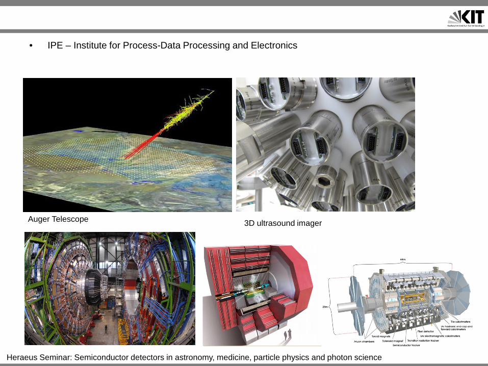
• IPE – Institute for Process-Data Processing and Electronics
Auger Telescope 3D ultrasound imager

Heraeus Seminar: Semiconductor detectors in astronomy, medicine, particle physics and photon science
• ASIC Design and Detector Technology group
PET Mu3e (HVCMOS)
Belle II PXD
CIX ROC

Heraeus Seminar: Semiconductor detectors in astronomy, medicine, particle physics and photon science 7
CMOS
Heraeus Seminar: Semiconductor detectors in astronomy, medicine, particle physics and photon science
CMOS
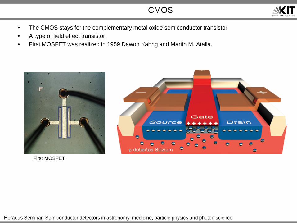
• The CMOS stays for the complementary metal oxide semiconductor transistor • A type of field effect transistor. • First MOSFET was realized in 1959 Dawon Kahng and Martin M. Atalla.
First MOSFET

Heraeus Seminar: Semiconductor detectors in astronomy, medicine, particle physics and photon science
MOS technology
• With development of ICs the MOSFET took the main role in electronics
First IC - Kilby Planar IC Noyce
CMOS IC
First microprocessor
Modern intel processor
Heraeus Seminar: Semiconductor detectors in astronomy, medicine, particle physics and photon science
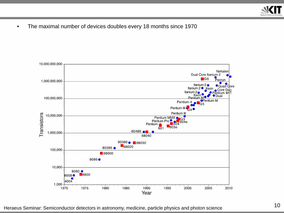
• The maximal number of devices doubles every 18 months since 1970
10

Heraeus Seminar: Semiconductor detectors in astronomy, medicine, particle physics and photon science
• The maximal number of devices doubles every 18 months since 1970
11

Heraeus Seminar: Semiconductor detectors in astronomy, medicine, particle physics and photon science 12
CMOS Sensors
Heraeus Seminar: Semiconductor detectors in astronomy, medicine, particle physics and photon science
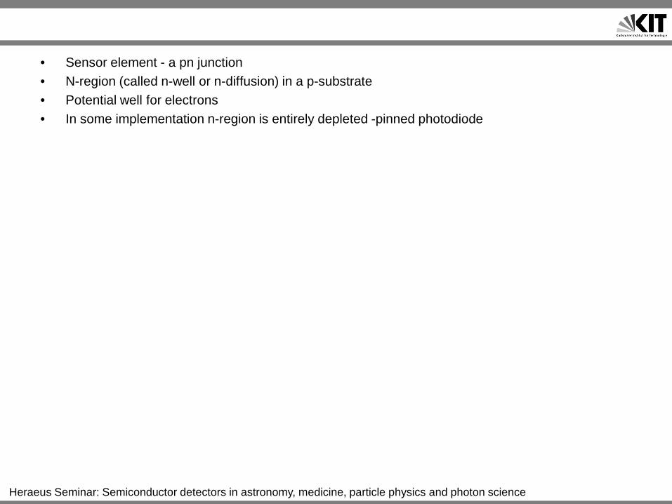
• Sensor element - a pn junction • N-region (called n-well or n-diffusion) in a p-substrate • Potential well for electrons • In some implementation n-region is entirely depleted -pinned photodiode

Heraeus Seminar: Semiconductor detectors in astronomy, medicine, particle physics and photon science
PN junction as sensor of radiation
• The pn-junction is reversely biased - depleted region, potential change, here depicted as the slope • 1. step - ionization
Atoms
Photons or particles
Ionisation Free e-

Heraeus Seminar: Semiconductor detectors in astronomy, medicine, particle physics and photon science
PN junction as sensor of radiation
• 2. step – charge collection • Two possibilities for charge collection – drift (through E-force) and by diffusion (density gradient)
Atoms
Collection of electrons

Heraeus Seminar: Semiconductor detectors in astronomy, medicine, particle physics and photon science
PN junction as sensor of radiation
• 3. step – charge to voltage conversion • Collection of the charge signal leads to the potential change
Atoms Potential change

Heraeus Seminar: Semiconductor detectors in astronomy, medicine, particle physics and photon science
MOS technology
• CMOS imaging sensors ,or CMOS pixel sensors, almost always contain at least one transistor inside a pixel. This transistor is acting as an amplifier

Heraeus Seminar: Semiconductor detectors in astronomy, medicine, particle physics and photon science
CMOS pixel
• Connection between the n-region (charge collecting electrode) and the gate of the transistor
N-type region Diffusion (shallow)
Or well (deep)
Sensor-junction MOS FET
Sensor-junction
MOS FET
Gate

Heraeus Seminar: Semiconductor detectors in astronomy, medicine, particle physics and photon science
CMOS pixel
• N in P diode acts as sensor element – signal collection electrode
N-type region Diffusion (shallow)
Or well (deep)
Sensor-junction MOS FET
Sensor-junction
MOS FET
Gate
Heraeus Seminar: Semiconductor detectors in astronomy, medicine, particle physics and photon science
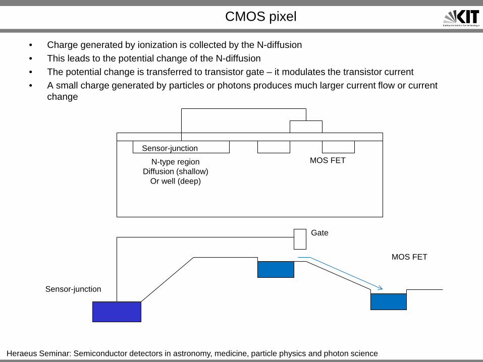
CMOS pixel
• Charge generated by ionization is collected by the N-diffusion • This leads to the potential change of the N-diffusion • The potential change is transferred to transistor gate – it modulates the transistor current • A small charge generated by particles or photons produces much larger current flow or current
change
N-type region Diffusion (shallow)
Or well (deep)
Sensor-junction MOS FET
Sensor-junction
MOS FET
Gate

Heraeus Seminar: Semiconductor detectors in astronomy, medicine, particle physics and photon science 21
Drift and Diffusion

Heraeus Seminar: Semiconductor detectors in astronomy, medicine, particle physics and photon science
CMOS pixel
• Charge generated in depletion region • Charges experience high field and holes are separated from electrons. Electrons move by drift
and are collected by the n-region
N-type region Diffusion (shallow)
Or well (deep)
Sensor-junction MOS FET
Sensor-junction
MOS FET
Gate
Heraeus Seminar: Semiconductor detectors in astronomy, medicine, particle physics and photon science
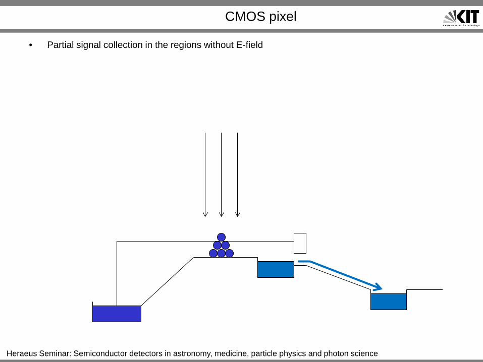
CMOS pixel
• Partial signal collection in the regions without E-field

Heraeus Seminar: Semiconductor detectors in astronomy, medicine, particle physics and photon science
CMOS pixel
• Partial signal collection in the regions without E-field
Recombination

Heraeus Seminar: Semiconductor detectors in astronomy, medicine, particle physics and photon science
CMOS pixel
• Partial signal collection in the regions without E-field
Recombination

Heraeus Seminar: Semiconductor detectors in astronomy, medicine, particle physics and photon science
CMOS pixel
• Partial signal collection in the regions without E-field
Charge collection by diffusion

Heraeus Seminar: Semiconductor detectors in astronomy, medicine, particle physics and photon science
CMOS pixel
• Partial signal collection in the regions without E-field
Charge collection by diffusion

Heraeus Seminar: Semiconductor detectors in astronomy, medicine, particle physics and photon science
• Differences between CMOS imaging sensors and CMOS particle sensors • CMOS imaging sensors are now the mostly used sensor type for digital cameras • Rolling shutter principle
A
A A A A A
Switch Switch
Pixel i+1 Pixel i Periphery of the chip

Heraeus Seminar: Semiconductor detectors in astronomy, medicine, particle physics and photon science
• Pixels of the same column share the same column line. • The gates of the switches are connected row-wise • For the readout of whole matrix we need n steps, where n is the number of rows. • Proper concept for imaging
A
A A A A A
Switch Switch
Pixel i+1 Pixel i Periphery of the chip

Heraeus Seminar: Semiconductor detectors in astronomy, medicine, particle physics and photon science 30
CMOS Sensors for Particle Physics

Heraeus Seminar: Semiconductor detectors in astronomy, medicine, particle physics and photon science
• Imaging sensors: efficiency 80% ok • Particle sensors: efficiency >99% required • Imaging sensors: detection of low energy photons • Particle sensors: detection of high energy ionizing particles • Imaging sensors: time resolution less important • Particle sensor: high time resolution is required • Output of imaging sensor pixel - amplified charge signal • Output of a smart particle sensor pixel - time information of (the triggered) hit
Heraeus Seminar: Semiconductor detectors in astronomy, medicine, particle physics and photon science 32
CMOS Sensors Types

Heraeus Seminar: Semiconductor detectors in astronomy, medicine, particle physics and photon science 33
MAPS

Heraeus Seminar: Semiconductor detectors in astronomy, medicine, particle physics and photon science 34
MOS pixel sensor with 100% fill factor - MAPS
MAPS
NMOS transistor in p-well N-well (collecting region) Pixel i
Charge collection (diffusion)
P-type epi-layer
P-type substrate Energy (e-)
• The collection electrode is near the electronics. • The charge collection is by diffusion. • Standard process. • Disadvantage: introduction of PMOS transistors lead to a charge loss • Lower radiation tolerance • Not a smart pixel • Still, very successful

Heraeus Seminar: Semiconductor detectors in astronomy, medicine, particle physics and photon science
MAPS
• IPHC Strasbourg (PICSEL group) • Family of MIMOSA chips • Applications:, STAR-detector (RHIC Brookhaven), Eudet beam-telescope
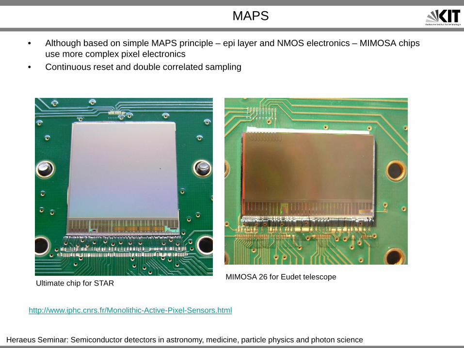
http://www.iphc.cnrs.fr/Monolithic-Active-Pixel-Sensors.html
Heraeus Seminar: Semiconductor detectors in astronomy, medicine, particle physics and photon science
MAPS
http://www.iphc.cnrs.fr/Monolithic-Active-Pixel-Sensors.html
Ultimate chip for STAR MIMOSA 26 for Eudet telescope
• Although based on simple MAPS principle – epi layer and NMOS electronics – MIMOSA chips use more complex pixel electronics
• Continuous reset and double correlated sampling

Heraeus Seminar: Semiconductor detectors in astronomy, medicine, particle physics and photon science
MAPS structure with CMOS pixel electronics
• If PMOS transistors are introduced, signal loss can happen
NMOS transistor in p-well
N-well (collecting region)
Pixel i
P-type epi-layer
P-type substrate Energy (e-)
MAPS with a PMOS transistor in pixel
PMOS transistor in n-well
Signal collection Signal loss

Heraeus Seminar: Semiconductor detectors in astronomy, medicine, particle physics and photon science 38
INMAPS
NMOS shielded by a deep p-well PMOS in a shallow p-well
N-well (collecting region)
Pixel
P-doped epi layer
INMPAS
• Deep P-layer is introduced to shield the PMOS transistors from epi layer • No charge loss occurs • Smart pixels possible • Not a CMOS standard process • Disadvantages are slow charge collection by diffusion and less radiation tolerance. Another
disadvantage is very limited number of producers and non-standard CMOS process

Heraeus Seminar: Semiconductor detectors in astronomy, medicine, particle physics and photon science
INMPAS
• INMAPS Tower Jazz process is gaining popularity in particle physics community • It was originally developed by the foundry and the Detector Systems Centre, Rutherford Appleton
Laboratory
2 Megapixels, large area sensor Designed for high-dynamic range X-ray imaging 40 µm pixel pitch 1350 x 1350 active pixels in focal plane Analogue readout Region-of-Reset setting 140 dB dynamic range 20 frames per second
??? chip
http://dsc.stfc.ac.uk/Capabilities/CMOS+Sensors+Design/Follow+us/19816.aspx

Heraeus Seminar: Semiconductor detectors in astronomy, medicine, particle physics and photon science
INMPAS
• Detector Systems Centre, Rutherford Appleton Laboratory – some examples
http://dsc.stfc.ac.uk/Capabilities/CMOS+Sensors+Design/Follow+us/19816.aspx
Wafer scale 120 x 145 mm chip for medical imaging
Heraeus Seminar: Semiconductor detectors in astronomy, medicine, particle physics and photon science 41
Depleted CMOS

Heraeus Seminar: Semiconductor detectors in astronomy, medicine, particle physics and photon science 42
Special Technologies

Heraeus Seminar: Semiconductor detectors in astronomy, medicine, particle physics and photon science 43
Depleted INMAPS - HRCMOS
• In depleted sensors charge is collected by drift -> faster signals • One of the first ideas is described in the PhD thesis of Walter Snoyes: „A new integrated pixel
detector for high energy physics“

Heraeus Seminar: Semiconductor detectors in astronomy, medicine, particle physics and photon science 44
Depleted INMAPS
NMOS shielded by a deep p-well PMOS in a shallow p-well
N-well (collecting region)
Pixel
• Improved version of INMAPS. Here a high voltage is used partially deplete the region underneath the electronics.
• Nonstandard CMOS

Heraeus Seminar: Semiconductor detectors in astronomy, medicine, particle physics and photon science 45
Depleted INMAPS
• Application: ALICE Upgrade

Heraeus Seminar: Semiconductor detectors in astronomy, medicine, particle physics and photon science 46
SOI technology
• Sensor part and the electronics are separated by oxide. The sensor has the form of a matrix of pn junctions, the collecting regions are p-type diffusion implants in the n-substrate. A connection through the buried oxide is made to connect the readout electronics with electrodes. SOI sensors are can use CMOS, the charge collection is based on drift. The disadvantage is a complex process.
Hi res. N
-type substrate E
lectronics layer B
uried oxide
Connection
Energy (h+)
CMOS pixel electronics
P+ collecting electrode
• Originally developed at University of Krakow • The development continued in collaboration
with industry (OKI and Lapis) • The collaboration is now led by KEK, Japan

Heraeus Seminar: Semiconductor detectors in astronomy, medicine, particle physics and photon science 47
SOI technology
• SOI technology can be used for x-ray detection thanks to its thick sensitive region • Example of an x-ray detector: INTPIX4
15.4 mm
10.2
mm

Heraeus Seminar: Semiconductor detectors in astronomy, medicine, particle physics and photon science 48
HVCMOS Depleted Sensors in Standard (Commercial)
Technologies

Heraeus Seminar: Semiconductor detectors in astronomy, medicine, particle physics and photon science 49
HVCMOS (HVMAPS) • HVCMOS is an attempt to implement CMOS depleted sensors in a standard process. • HVCMOS uses one trick; the electronics is placed directly inside the collecting electrode.
Transistors sense the tiny voltage change in their environment • Since electronics is placed in the n-well the substrate is decoupled from the electronics • It can be put on high negative potential and a large drift field is induced. • This makes HVCMOS sensors very radiation tolerant. • HVCMOS are based on a standard process. They are therefore cheap
P-Substrate
Depleted zone
“Smart” Diode
n-Wanne
Pixel
HVCMOS Detector
Drift Ppotential energy (e-)

Heraeus Seminar: Semiconductor detectors in astronomy, medicine, particle physics and photon science 50
HVCMOS (HVMAPS) • HVCMOS is an attempt to implement CMOS depleted sensors in a standard process. • HVCMOS uses one trick; the electronics is placed directly inside the collecting electrode.
Transistors sense the tiny voltage change in their environment • Since electronics is placed in the n-well the substrate is decoupled from the electronics • It can be put on high negative potential and a large drift field is induced. • This makes HVCMOS sensors very radiation tolerant. • HVCMOS are based on a standard process. They are therefore cheap
P-Substrate
Depleted
n-Wanne
Drift N-well (collecting region)
P-type epi-layer
P-type substrate

Heraeus Seminar: Semiconductor detectors in astronomy, medicine, particle physics and photon science
3D layout of a “smart diode”
40 µm
3D layout generated by GDS2POV software
Heraeus Seminar: Semiconductor detectors in astronomy, medicine, particle physics and photon science 52
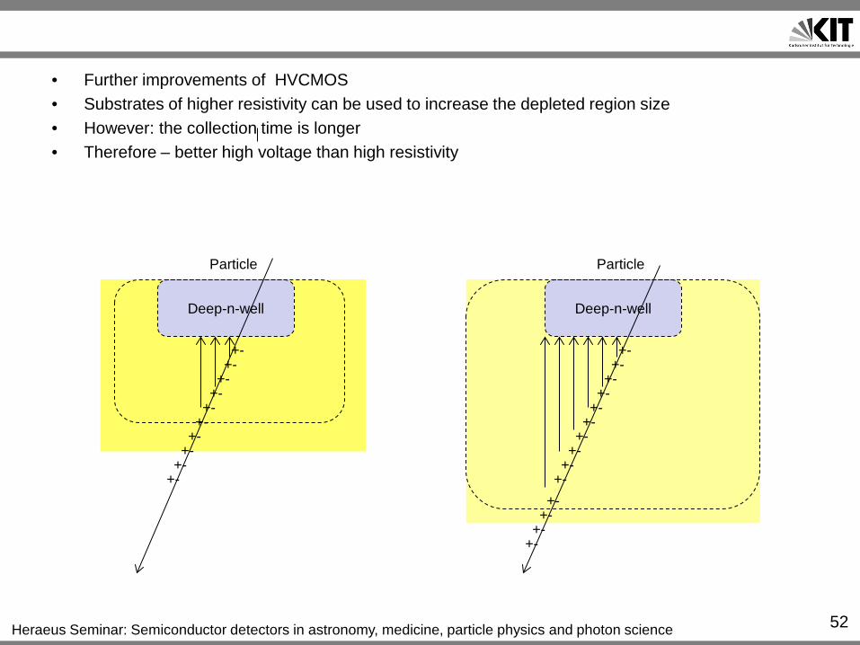
• Further improvements of HVCMOS • Substrates of higher resistivity can be used to increase the depleted region size • However: the collection time is longer • Therefore – better high voltage than high resistivity
Deep-n-well
+- +-
+- +-
+- +-
+- +-
+- +-
Deep-n-well
+- +-
+- +-
+- +-
+- +-
+- +-
+- +-
+- +-
Particle Particle

Heraeus Seminar: Semiconductor detectors in astronomy, medicine, particle physics and photon science 53
• For radiation tolerant sensors, substrate resistivity of 100 Ωcm is probably optimal
Compare measured/calculated After a certain dose, we expect that all substrates behave similarly ~100 Ohm cm probably the best chioce
Heraeus Seminar: Semiconductor detectors in astronomy, medicine, particle physics and photon science 54
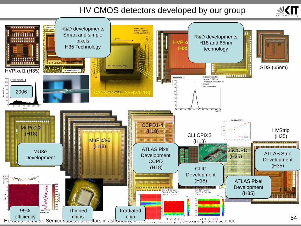
HV CMOS detectors developed by our group
CAPSENS (0.35HV/0.18)
HVPixel1 (H35)
0 50 100 150 200 250 3000
200
400
600
800
1000
1200
1400Fe-55, Diode, 55V
Num
ber o
f hits
ToT/Clk
HVPixel2 (CCPD)
HVPixelM (H35)
Hpixel (H18)
SDS (65nm)
MuPix1/2 (H18)
MuPix3-6 (H18)
CCPD1-4 (H18)
CLIICPIXS (H18)
H35CCPD (H35)
HVStrip (H35)
R&D developments Smart and simple
pixels H35 Technology
R&D developments H18 and 65nm
technology
MU3e Development
ATLAS Pixel Development
CCPD (H18) CLIC
Development (H18) ATLAS Pixel
Development (H35)
ATLAS Strip Development
(H35)
2006
99% efficiency
Thinned chips
Irradiated chip

Heraeus Seminar: Semiconductor detectors in astronomy, medicine, particle physics and photon science
HV CMOS detectors developed by our group
• Demonstrator in AMS H35: Collaboration: Barcelona, Bern, Geneva, KIT, Liverpool • Implemented at four different substrates: 20, 80, 200 and 1 kΩ cm
55

Heraeus Seminar: Semiconductor detectors in astronomy, medicine, particle physics and photon science 56
• The development of HVCMOS sensors started as a small project. • Now they are developed within several collaborations: • Mu3e collaboration (Heidelberg, PSI, KIT, University ETH Zuerich) • ATLAS CMOS demonstrator collaboration • ATLAS CMOS strip collaboration • CLIC detector R&D group • ATLAS HVMAPS collaboration

Heraeus Seminar: Semiconductor detectors in astronomy, medicine, particle physics and photon science 57
CLIC
Heraeus Seminar: Semiconductor detectors in astronomy, medicine, particle physics and photon science 58
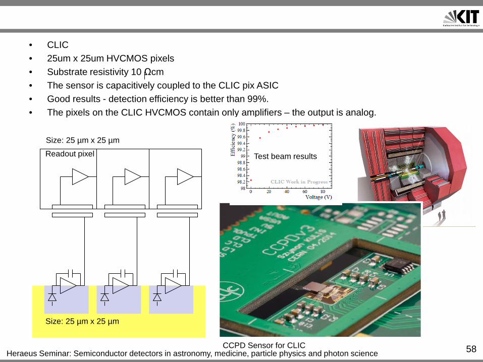
• CLIC • 25um x 25um HVCMOS pixels • Substrate resistivity 10 Ωcm • The sensor is capacitively coupled to the CLIC pix ASIC • Good results - detection efficiency is better than 99%. • The pixels on the CLIC HVCMOS contain only amplifiers – the output is analog.
Readout pixel
Size: 25 µm x 25 µm
Size: 25 µm x 25 µm
CCPD Sensor for CLIC
Test beam results

Heraeus Seminar: Semiconductor detectors in astronomy, medicine, particle physics and photon science 59
Mu3e
Heraeus Seminar: Semiconductor detectors in astronomy, medicine, particle physics and photon science 60
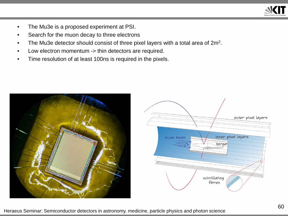
• The Mu3e is a proposed experiment at PSI. • Search for the muon decay to three electrons • The Mu3e detector should consist of three pixel layers with a total area of 2m2. • Low electron momentum -> thin detectors are required. • Time resolution of at least 100ns is required in the pixels.

Heraeus Seminar: Semiconductor detectors in astronomy, medicine, particle physics and photon science 61
• We have developed within several iterations a monolithic pixel sensor. It is a system on a chip - the readout electronics is placed on the same chip as the sensors. The signals are directly sent to FPGAs via GBit links. We measure 99% efficiency in beam tests
• Thinned chips successfully tested • 10 Ωcm
MuPixel
Test of a thinned chip <100um
Kapton cable
1.25GBit/s data transmission

Heraeus Seminar: Semiconductor detectors in astronomy, medicine, particle physics and photon science 62
• We have developed within several iterations a monolithic pixel sensor. It is a system on a chip - the readout electronics is placed on the same chip as the sensors. The signals are directly sent to FPGAs via GBit links. We measure 99% efficiency in beam tests.
>99% detector effeiciency

Heraeus Seminar: Semiconductor detectors in astronomy, medicine, particle physics and photon science 63
ATLAS

Heraeus Seminar: Semiconductor detectors in astronomy, medicine, particle physics and photon science 64
• HVCMOS is also investigated for ATLAS upgrade, both for pixel and strip layers. • Two concepts • 1. The more conservative concept is to keep the existing readout chips, with slight modifications,
and to replace the existing planar pixel or strip sensors with so called smart HVCMOS sensors • 2. Monolithic sensors

Heraeus Seminar: Semiconductor detectors in astronomy, medicine, particle physics and photon science 65
CCPD Pixels
Heraeus Seminar: Semiconductor detectors in astronomy, medicine, particle physics and photon science 66
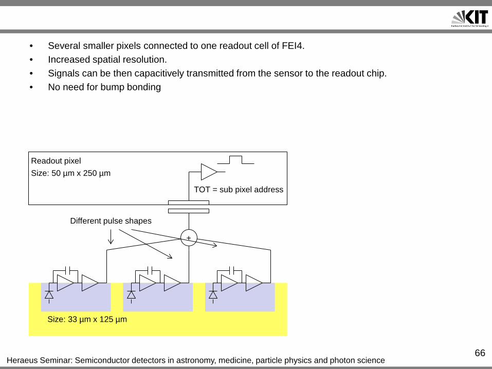
• Several smaller pixels connected to one readout cell of FEI4. • Increased spatial resolution. • Signals can be then capacitively transmitted from the sensor to the readout chip. • No need for bump bonding
+
TOT = sub pixel address
Readout pixel Size: 50 µm x 250 µm
Size: 33 µm x 125 µm
Different pulse shapes
Heraeus Seminar: Semiconductor detectors in astronomy, medicine, particle physics and photon science
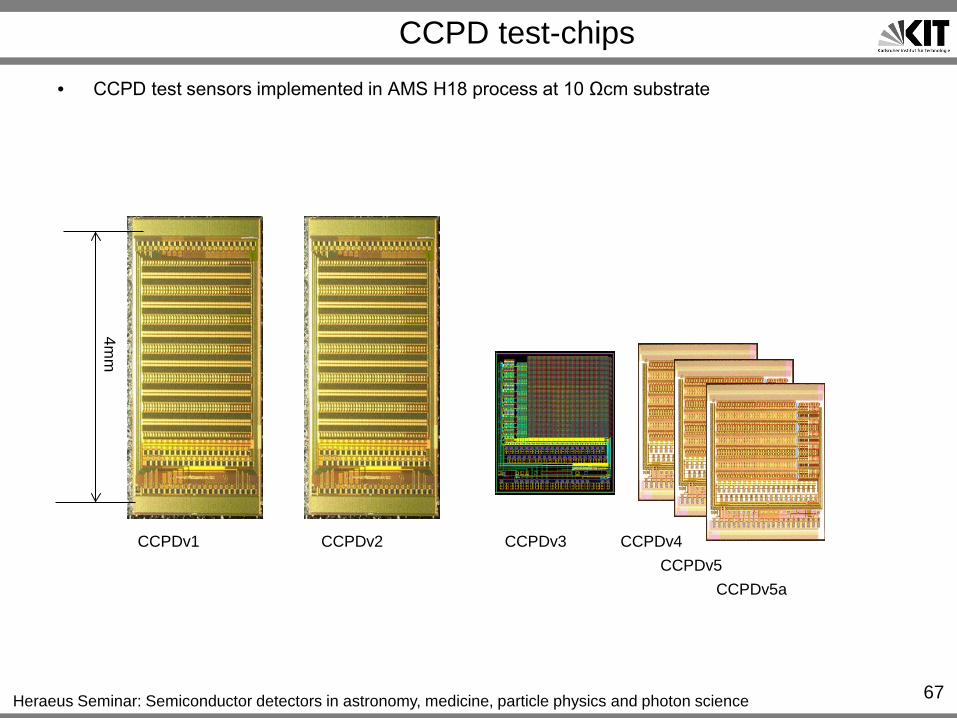
CCPD test-chips • CCPD test sensors implemented in AMS H18 process at 10 Ωcm substrate
67
CCPDv1 CCPDv2 CCPDv3 CCPDv4
4mm
CCPDv5 CCPDv5a

Heraeus Seminar: Semiconductor detectors in astronomy, medicine, particle physics and photon science 68
• >99% detection efficiency before irradiation • Several chips irradiated with neutrons at Jozef Stefan institute in Ljubljana. • Detection efficiency with an irradiated chip (fluence 1015 neq) 96% • Bias voltage was reduced – 12V
Efficiency of more than 99 % has been measured by University of Geneva with unirradiated chips and 96% with the chips irradiated to 1015 neq/cm2 with neutrons

Heraeus Seminar: Semiconductor detectors in astronomy, medicine, particle physics and photon science 69
Thank you

Heraeus Seminar: Semiconductor detectors in astronomy, medicine, particle physics and photon science 70
CMOS Strips

Heraeus Seminar: Semiconductor detectors in astronomy, medicine, particle physics and photon science 71
• In the case of strips, hit data are sent in digital format to the external chip that does the triggering. HVCMOS replacement for the strip sensor is actually a pixel sensor with long pixels.
• The advantages over the present concept is the z-resolution with one layer, less number of wire bonds between the sensor and the digital readout chip, and a simplified readout chip which is only digital.
Pixel contains a charge sensitive amplifier
CSA
A C5 DB
Output 1
Output 2
0 10
C5
y5
A C DB
y2
y3
Output 1
Output 2
0 1 2
A2
B3

Heraeus Seminar: Semiconductor detectors in astronomy, medicine, particle physics and photon science 72
• In the case of strips, hit data are sent in digital format to the external chip that does the triggering. HVCMOS replacement for the strip sensor is actually a pixel sensor with long pixels.
• The advantages over the present concept is the z-resolution with one layer, less number of wire bonds between the sensor and the digital readout chip, and a simplified readout chip which is only digital.
Pixel contains a charge sensitive amplifier
CSA
HVStripV1, irradiated to 2 x 10¹⁵neq/cm2 - MPW of Sr-90 spectrum vs. sensor bias.
HVStripV1, irradiated to 2 x 10¹⁵neq/cm2 and 60 MRad – NMOS characteristics.

Heraeus Seminar: Semiconductor detectors in astronomy, medicine, particle physics and photon science 73
Radiation Tolerance

Heraeus Seminar: Semiconductor detectors in astronomy, medicine, particle physics and photon science 74
• Radiation tolerance
Spectrum of beta particle signals when a HVStripV1, irradiated to 2 x 10¹⁵neq/cm2 is exposed to Sr-90 source. Calibration x-ray spectra are also shown. Strontium-90 signal after proton irradiation to 2 x 10¹⁵neq/cm2 ~ 3600e. Signal to noise ratio after proton irradiation ~ 20.
Charge vs. fluence
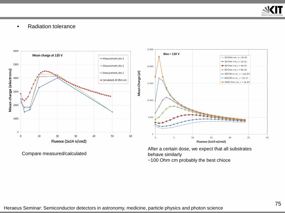
Heraeus Seminar: Semiconductor detectors in astronomy, medicine, particle physics and photon science 75
• Radiation tolerance
Compare measured/calculated After a certain dose, we expect that all substrates behave similarly ~100 Ohm cm probably the best chioce

Heraeus Seminar: Semiconductor detectors in astronomy, medicine, particle physics and photon science 76
Time Resolution

Heraeus Seminar: Semiconductor detectors in astronomy, medicine, particle physics and photon science
Time resolution • Time resolution in test beam measurements was about 100ns – we need 25ns • This time uncertainty is mostly caused by the time walk effect • The problem is that the preamplifier is designed to have a peaking time > 100ns. • Using of long peaking time allows us to operate the detector in low-power mode – long peaking
time reduces noise for an equal bias current (power). However if the signal spread is large (landau distribution, we will have a time walk – time skew.
77
TW
Tpeak
Th
Sig

Heraeus Seminar: Semiconductor detectors in astronomy, medicine, particle physics and photon science
• There are a few way to improve time resolution • One is to make the amplifier faster. This is possible, however it increases the noise. If we make
amplifier faster we will probably need to increase the signal – which can be done by using high resistive substrate.
• More elegant way to improve the timing - compensation • Bases of the fact that the time walk is proportional to the signal amplitude
78

Heraeus Seminar: Semiconductor detectors in astronomy, medicine, particle physics and photon science
• Idea: time walk compensating comparator. Rise time is longer for signal with high amplitudes. This means a signal with higher amplitude has a faster threshold crossing, but the comparator output is slower.
• A signal with lower amplitude has a later threshold crossing but the comparator output is faster. As consequence of this the comparator outputs for all amplitudes can cross in one point. By adding another comparator we can make the response time independent of amplitude.
79
Slow down
Slow down
Higher amplitude
Lower amplitude
2

Heraeus Seminar: Semiconductor detectors in astronomy, medicine, particle physics and photon science
• Idea: time walk compensating comparator. Rise time is longer for signal with high amplitudes. This means a signal with higher amplitude has a faster threshold crossing, but the comparator output is slower.
• A signal with lower amplitude has a later threshold crossing but the comparator output is faster. As consequence of this the comparator outputs for all amplitudes can cross in one point. By adding another comparator we can make the response time independent of amplitude.
80
Amplifier response to signals from 1000e to 3800e
Comparator response to signals from 1000e to 3800e
100ns 15ns