pÁginas 1-74 - rmf.smf.mx · universidad de la frontera, chile ivan l’heureux university of...
TRANSCRIPT
REVISTA MEXICANA DE FÍSICA S ABRILVOL. 57 NUM. 2 2011 PÁGINAS 1-74
ISSN 0035-00IX
VOLUMEN 57
NUMERO 2
ABRIL 2011
PÁGINAS 1-74
CODEN: RMFXFATEjemplar $170.00
PÁGINAS 1-74
VOLUMEN 57
NUMERO 2
ABRIL
2011
PÁGINAS 1-74
REVISTA MEXICANA DE FÍSICA S
Abril 2011
REVISTA MEXICANA DE FÍSICA S
Abril 2011
www.smf.mx/rmf/

REVISTA MEXICANA DE FISICADirector:Fransisco Ramos GomezFacultad de Ciencias, UNAM, Mexico
Consejeros EmeritosMarcos MoshinskyInstituto de Fısica, UNAM, Mexico
Leopoldo Garcıa-ColınUniversidad Autonoma Metropolitana – Iztapalapa, Mexico
Manuel PeimbertInstituto de Astronomıa UNAM, Mexico
Fernando AlbaInstituto de Fısica, UNAM, Mexico
Consejo Editorial
Materia Condensada:Carlos BalseiroCentro Atomico de Bariloche, Argentina
Alipio G. CallesFacultad de Ciencias, UNAM, Mexico
Manuel CardonaInstitute Max Planck, Stuttgart, Alemania
Robert CavaUniversity of Princeton, USA
Roberto EscuderoInstituto de Investigaciones en Materiales, UNAM, Mexico
Francisco JaqueUniversidad Autonoma de Madrid, Espana
Harold KrotoFlorida State University
Fısica Atomica y Molecular:Gerardo Delgado-BarrioConsejo Superior de Investigacion Cientıfica, Espana
James McGuireTulane University, USA
Alfred SchlachterAdvanced Light Source, LBL Berkeley California, USA
Fısica Nuclear:Alejandro FrankInstituto de Ciencias Nucleares, UNAM, Mexico
Arturo MenchacaInstituto de Fısica, UNAM, Mexico
Andres SandovalGSI, Alemania & CERN, Suiza
Termodinamica y Fısica Estadıstica:Eugenio E. VogelUniversidad de la Frontera, Chile
Ivan L’heureuxUniversity of Ottawa, Canada
Vıctor RomeroInstituto de Fısica, UNAM, Mexico
Optica:Alejandro CornejoInstituto Nacional de Astrofısica, Optica y Electronica, Mexico
Eugenio MendezCICESE, Mexico
Jumpei TsujiuchiInstitute of Technology, Tokio, Japon
Fernando MendozaCentro de Investigaciones en Optica, Mexico
Gravitacion y Fısica Matematica:Octavio ObregonInstituto de Fısica, Universidad de Guanajuato, Mexico
Fernando QuevedoUniversity of Cambridge, Inglaterra
Instrumentacion:Victor CastanoCentro de Fısica Aplicada y Tecnologıa Avanzada, UNAM, Mexico
Daniele FinotelloKent State University, USA
Partıculas Elementales y Teorıa de Campo:Gerardo Herrera CorralCINVESTAV, IPN, Mexico
Fısica Medica:Marıa Ester BrandanInstituto de Fısica, UNAM, Mexico
Secretaria:Marıa Magdalena Lopez ReynosoSociedad Mexicana de Fısica
Revision de Estilo:Jose Luis Alvarez GarcıaFacultad de Ciencias, UNAM
Juan Pablo Flores del VillarSociedad Mexicana de Fısica
Edicion Tecnica:Raul A. Espejel MoralesFacultad de Ciencias, UNAM
Asistentes Tecnicos:Efraın R. Garrido RomanSociedad Mexicana de Fısica
Paris M. Sanchez CarreonSociedad Mexicana de Fısica
La Revista Mexicana de Fısica es una publicacion bimestral de la Sociedad Mexicana de Fısica, A.C., Apartado Postal 70-348, Coyoacan,04511 Mexico, D.F., MEXICO. Se publica con el patrocinio de: Instituto Nacional de Astrofısica Optica y Electronica, Puebla, InstitutoPotosino de Investigacion Cientıfica y Tecnologica, San Luis Potosı, y de la UNAM: Rectorıa, Coordinacion de la Investigacion Cientıfica,Instituto de Astronomıa, Centro de Ciencias de la Materia Condensada, Instituto de Ciencias Nucleares, Instituto de Investigaciones enMateriales, Instituto de Fısica, Facultad de Ciencias e Instituto de Matematicas.
Indizada en: Actualidad Iberoamericana, Astron. & Astrophys. Abstr., Bull. Signal., Chem. Abstr., Curr. Cont., Curr. Math. Pub., Curr.Pap. Phys., Electr. & Electron. Abstr., INIS Atomind., Math. Sci., LatIndex, Math. Rev., Nucl. Sci. Abstr., PERIODICA, Phys. Abstr.,Phys. Ber., Res. Alert, Sci. Abstr., Sci. Cit. Ind., y SciSearch. Incluida en el Indice de Revistas Mexicanas de Investigacion Cientıfica yTecnologica del Consejo Nacional de Ciencia y Tecnologıa (CONACyT).
Las instrucciones para autores aparecen publicadas en el numero 6 de cada volumen. El costo de la suscripcion anual es de $1000.00 pesospara la Republica Mexicana, $130 USD para America Central y del Norte y $160 USD para el resto del mundo. Precio del ejemplar $170.00pesos.

Revista Mexicana de Fısica S ISSN–0035–00IX
Publicacion de la Sociedad Mexicana de Fısica, A.C.Apartado postal 70-348, Coyoacan, 04510 Mexico, D.F.
Director : Fransisco Ramos Gomez
Oficinas: 2 piso, Departamento de Fısica, Facultad de Ciencias, Ciudad Universitaria, 04510Mexico, D.F. Tel.: (55) 5622-4946; FAX: (55) 5622-4848.
Se autoriza la reproduccion parcial o total de su contenido citando la fuente: Rev. Mex. Fis S.Los artıculos firmados son responsabilidad de los autores.
Certificado de licitud numero 3110 y de contenido numero 2775 otorgado por la ComisionCalificadora de Publicaciones y Revistas Ilustradas de la Secretarıa de Gobernacion. Reservadel tıtulo numero 68–88 de la Direccion General de Derechos de Autor. Publicacion periodica:Registro numero 038 0488, caracterısticas 210241109, otorgado por la oficina del ServicioPostal Mexicano.
El volumen 57, numero 2, abril de 2011, se termino de imprimir en abril de 2011; se tiraron500 ejemplares.
Impresion: Impresiones Integradas del Sur, S.A. de C.V., Amatl No. 20, Col. Santo Domingo,Delegacion Coyoacan, 04369 Mexico, D.F., Tel.: 5619-4088.
Diseno de portada: Arte Grafico, Sur 71 No. 501, Col. Justo Sierra, 09460 Mexico, D.F.
Impreso en Mexico–Printed in Mexico

i
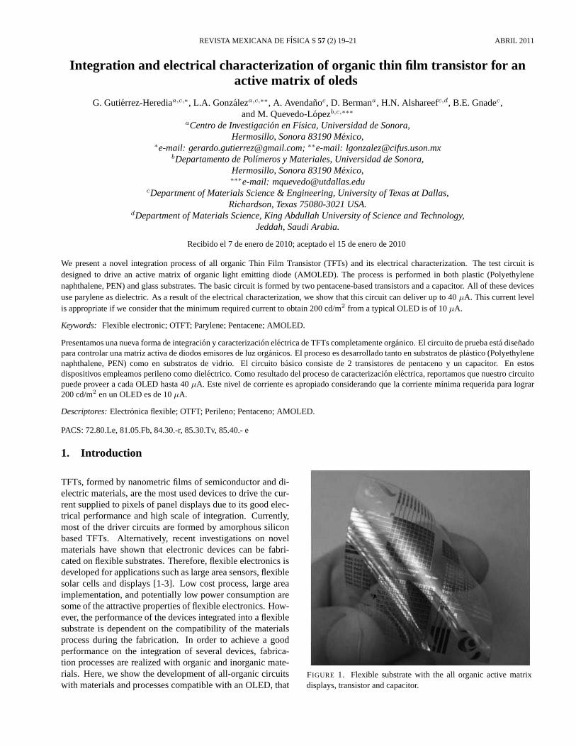
VI International Topical Meeting on Nanostructured Materialsand Nanotechnology, Nanotech 2009
San Carlos, Nuevo GuaymasSeptember 17-19, 2010
Editor:
RAFAEL GARCIA GUTIERREZ

ii
ORGANIZING COMMITTEE
Rafael Garcıa Gutierrez
Alvaro Posada Amarillas
Elder de la Rosa Cruz
Marcelino Barboza Flores

iii
PREFACIO
El Sexto Encuentro Internacional sobre Materiales Nanoestructurados y Nanotec-nologıa, NANOTECH 2009, es un congreso internacional que se ha organizado enla Republica Mexicana desde el ano 2004. La primera reunion se llevo a cabo enlas instalaciones del Centro de Investigacion enOptica, en Leon, Guanajuato. Enel 2005 se organizo en el Centro de Ciencias de la Materia Condensada-UNAMen Ensenada. En el 2006 se llevo a cabo en la ciudad de Puebla en el Institutode Fısica-BUAP. Monterrey fue la sede de la organizacion de la Conferencia del2007, en las instalaciones de la Universidad Autonoma de Nuevo Leon. En el2008 el congreso se celebro en Ciudad Universitaria-UNAM en Mexico D.F. Enesta ocasion la reunion fue organizada del 17 al 19 de septiembre del 2009 porel Departamento de Investigacion en Fısica de la Universidad de Sonora en SanCarlos Nuevo Guaymas. El congreso fue el escenario para la presentacion de 2cursos cortos, 2 mesas redondas para tratar los temas de las aplicaciones de lananotecnologıa en la industria, 15 exposiciones orales y 88 carteles, ademas de 10conferencias magistrales presentadas por empresarios sonorenses y cientıficos derenombre mundial.
El objetivo principal del NANOTECH 2009 fue el de proporcionar un foropara que cientıficos, ingenieros y empresarios busquen solucion a problemas cientı-ficos que conduzcan a aplicaciones practicas. Los topicos que se trataron en dichoevento comprendieron desde ciencia basica hasta aplicaciones y tecnicas de com-ercializacion de alta tecnologıa. Algunos de los principales temas discutidos aquıfueron los nanotubos de carbono, nanomateriales magneticos y nanoestructurasmetalicas (plasmones), celdas solares y de combustible, nanofosforos incluyendooxidos, nitruros, tierras raras, y organicos; nanomedicina, nanocristales lineales yno lineales y cristales fotonicos.
El comite organizador agradece profundamente el apoyo financiero otorgadopor la Universidad de Sonora, la Direccion Adjunta de Desarrollo Cientıfico yAcademico, CONACYT (Mexico), Red Tematica de Nanociencias y Nanotec-nologıa, y las empresas, Rubio Pharma y Asociados y RD Research & Technology.

REVISTA MEXICANA DE FISICA S57 (2) 1–6 ABRIL 2011
Catalytic activity of MoS 2 nanotubes in the hydrodesulphurizationreaction of dibenzothiophene
F. Leonard-Deepaka,b, R.Perez-Hernandezb,c, J. Cruz-Reyesd, S. Fuentese, and M.J. Yacaman∗,baInternational Iberian Nanotechnology Laboratory,
Avda Mestre Jose Veiga, Braga 4715, Portugal.bDepartment of Physics and Astronomy, One UTSA Circle,The University of Texas at San Antonio, Texas, 78249, USA,
cInstituto Nacional de Investigaciones Nucleares,Carr. Mexico-Toluca S/N La Marquesa, Ocoyoacac, Edo. de Mexico 52750, Mexico.
dFacultad de Ciencias Quımicas e Ingenierıa, Universidad Autonoma de Baja California,Tijuana, B.C., Mexico.
e Centro de Nanociencias y Nanotecnologıa de la Universidad Nacional Autonoma de Mexico,Km. 107 Carretera Tijuana-Ensenada, Apartado Postal, 356, Ensenada, B.C., 22800, Mexico.
Recibido el 20 de noviembre de 2009; aceptado el 18 de enero de 2010
In the need for developing better fuels and as a consequence better hydrodesulphurization catalysts (HDS), new generations of catalystsare necessary to reduce substantially the sulfur content in diesel and gasoline fuels. HDS are catalytic processes that involve Mo or W-based catalysts, often doped with other transition metals. We synthesized MoS2 nanotubes by reacting MoO3 with thiourea and usedthem as catalysts for the hydrodesulfurization of dibenzothiophene in a batch reactor. X-ray diffraction, scanning electron microscopy, andtransmission electron microscopy techniques were used to characterize their morphology and structure. The results indicated the hexagonalcrystalline structure of MoS2 and large yields of the MoS2 nanotubes with unusual square or rhomboid faceted shapes. The catalyticbehavior of the MoS2 nanotube catalysts showed that the direct desulfurization pathway prevailed over the hydrogenation (HYD) pathway.This finding was attributed to the low rim/edge sites ratio, induced by the size and morphology of the nanotubes showing large flat area whichis responsible for the biphenyl (BP) selectivity.
Keywords: Hydrodesulfurization; selectivity; dibenzothiophene (DBT); molybdenum sulfide (MoS2); nanotubes; TEM.
En la necesidad de desarrollar mejores combustibles y como consecuencia mejores catalizadores para la hidrodesulfuracion (HDS), nuevasgeneraciones de catalizadores son necesarios para reducir sustancialmente el contenido de azufre en los combustibles diesel y gasolina.HDS es un proceso catalıtico que involucra catalizadores basados en Mo y W, a menudo dopados con otros metales de transicion. Sesintetizaron nanotubos de MoS2 reaccionando MoO3 con thiourea. Los nanotubos se utilizaron como catalizadores para la hidrodesulturacionde dibenzotiofeno en un reactor discontinuo (batch reactor). Las tecnicas de difraccion de rayos X, microscopıa electronica de barrido y detransmision fueron utilizadas para caracterizar la morfologıa y la estructura de los catalizadores. Los resultados mostraron la estructuracristalina hexagonal del MoS2 y grandes rendimientos de nanotubos de MoS2 con formas facetadas cuadradas o romboidales inusuales. Elcomportamiento catalıtico de los nanotubos de MoS2 demostro que la vıa de desulfuracion directa prevalecio sobre la vıa de hidrogenacion(HYD). Este resultado se atribuyo a la baja relacion diametro/superficie (rim/edge), inducida por el tamano y morfologıa de los nanotubos,mostrando unarea grande y plana, que es la responsable de la selectividad del bifenilo (BP).
Descriptores:hidrodesulfuracion; selectividad; dibenzotiofeno; sulfuro de molibdeno (MoS2); MET.
PACS: 81.16.Hc, 61.05.cp, 68.37.Lp, 68.37.Og
1. Introduction
Elimination of sulfur from petroleum feedstocks is necessaryin order to meet the severe restrictions on the sulfur con-centrations in fuels [1,2]. The hydrodesulfurization (HDS)of polyaromatic sulfur compounds or deep HDS is espe-cially difficult for the case of heavy oils containing highconcentration of sulfur (2–3 wt %). Catalysts based onmolybdenum sulfide are widely used in oil refineries forthe HDS, hydrodenitrogenation (HDN) and hydrodeoxygena-tion (HDO) reactions of petroleum-derived feedstocks [3-5].Due to the stringent environmental legislation that set thesulfur level at ¡ 15 ppm, new catalysts with significantlyimproved catalytic performance must be developed. Sul-fur compounds that are known to remain in fuels such as
diesel at sulfur levels below 500 ppm include dibenzoth-iophene (DBT) and alkyl-substituted DBT’s such as 4,6-dimethyldibenzothiophene (4,6-DMDBT) [6,7]. The HDSgenerally proceeds through two pathways: a hydrogenation(HYD) pathway involving aromatic ring hydrogenation anda hydrogenolysis pathway via direct C–S bond cleavage, alsocalled the direct desulfurization (DDS) pathway [8]. Thecontribution of both pathways defining the selectivity de-pends on the catalyst type. The HDS of DBT in CoMocatalysts occurs predominantly via the DDS pathway yield-ing HYD/DDS ratios from 0.3 to 0.5. However, for theHDS of 4,6-DMDBT [5], due to the steric hindrance of themethyl groups it is necessary for the hydrogenation of atleast one aromatic ring before the elimination of sulfur. In

2 F.L. DEEPAK, R.P. HERNANDEZ, J. CRUZ-REYES, S. FUENTES, AND M.J. YACAMAN
that case, new catalysts with higher specific hydrogenoly-sis activity and/or higher hydrogenation activity are required.The addition of acid functionality through the use of zeo-lite [9-11] or amorphous alumina-silicate supports [11,12]to the standard promoted molybdenum sulfide-based cata-lysts led to noticeable enhancement in the HDS of alkyl-substituted DBT enabling the dealkylation and isomerizationof the alkyl substituents, thereby transforming the refractorycomponents into more reactive species. Acidic supports havealso improved the catalytic performance of the catalyst par-ticles by increasing their electron deficient character, result-ing in greater sulfur resistance and intrinsic activity [13-15].However, support acidity is also associated with catalyst de-activation by coke formation [16], a phenomenon that led tonumerous efforts to fine-tune the effects of the support acid-ity [17-21].
MoS2 nanoparticles can have different morphologies de-pending on the preparation conditions (nanotubes, nanorods,onion-like nanoparticles, 2D nanoparticles, etc). All the mor-phologies are derived from its layer structure in which atomswithin a layer are bound by strong covalent forces, while in-dividual layers are held together by van der Waals interac-tions. The stacking sequence of the layers can lead to theformation of either a hexagonal polymorph with two layersin the unit cell (2H), rhombohedral with three layers (3R)or trigonal with one layer (1T). Nanotubes of the transitionmetal dichalcogenides (ex: MoS2, WS2) have attracted con-siderable attention in recent years [22-26]. One of the firstmethods of synthesis of MoS2 nanotubes was developed byFeldman,et al. [27]. This method involved the gas-phasereaction of MoO3−x and H2S at 850C in a reducing at-mosphere. Nath,et al. [28] used thermal decomposition ofammonium thiomolybdate at higher temperatures, which re-sulted in the formation of MoS2 nanotubes. Li,et al. [29]have developed an atmospheric pressure chemical vapor de-position (APCVD) route for the synthesis of MoS2 nanos-tructures. These nanostructures, including three-dimensionalnanoflowers (NF), were obtained by the reaction of chlo-rides (MoCl5) and sulfur, under controlled conditions. Themeasured surface area and field emission of these nanostruc-tures showed them to be promising candidates as catalysts.In all the methods of synthesis outlined so far, the reducing-sulphidizing agents included H2S (or a mixture of H2 andH2S) and S powder. In general, the methods of synthesis ofMoS2 nanotubes obtained them in low yields (∼20 %) aswell as by long tedious procedures (ex: two-stage synthesis).The most important application of MoS2 is as catalyst for theHDS of fuels, typically, they are evaluated in model test re-actions as the HDS of thiophene, dibenzothiophene and 4,6DMDBT [30-34]. In order to scale the use of MoS2 nan-otubes in catalysis or other applications it is important to de-vise new synthetic routes to obtain them in large yields. Thepresent work proposes a simple one step synthetic process,using thiourea and MoO3 as the starting materials to producelarge quantities of MoS2 nanotubes. The resulting nanotubeshave unusual faceted shapes (square or rhomboid) which are
reported here for the first time. Thiourea has not been em-ployed previously as a sulphur source for making MoS2 nan-otubes; it generates a suitable reducing-sulphidizing environ-ment in-situ, eliminating the use of a separate reducing agent.
2. Experimental methods and characteriza-tion
2.1. Synthesis
Synthesis of the MoS2 nanotubes was carried out as follows.About 0.6 g of MoO3 (mp = 795C) and 1.0 g of thiourea(CSN2H4,mp = 170-176C) were placed in an alumina boat(ratio of Mo:S was kept at∼ 1:2.5 to ensure an excess ofthe sulphur source). The boat was placed in an alumina tubeat the heating zone of a horizontal furnace. Before the re-action the system was flushed with N2 for 1/2 hr to removeany traces of oxygen. The tube was then heated to 1000C inflowing N2 (flow rate = 200 cc/min) [35]. Previously cleanedsilicon substrates were placed at regular intervals in the outletregion of the alumina tube to collect the product as a depositduring the course of the reaction. The reaction was carriedout for 1 hr, after which it was gradually cooled down to roomtemperature in flowing N2. At the end of the reaction the re-sulting grey colored powder was collected from the aluminaboat and the silicon substrate (nanotubes) for further analysis.
2.2. Characterization
X-ray diffraction (XRD) powder patterns were recorded in aSiemens D-5000 diffratometer, using Cu Kα (λ=0.15406 nm)radiation. Scanning electron microscopy (SEM) was per-formed in a FEG Hitachi S-5500 ultra high resolution elec-tron microscope (0.4 nm at 30 kV) with a BF/DF Duo-STEMdetector. Transmission electron microscopy (TEM) and se-lected area electron diffraction (SAED) were performed us-ing a Tecnai 20 TEM equipped with a Schottky-type fieldemission gun, ultra-high resolution pole piece (Cs=0.5 mm),and a scanning transmission electron microscope (STEM)unit with high angle annular dark field (HAADF) detectoroperating at 200 kV.
2.3. Catalytic experiments
The HDS of DBT was tested in a 300 mL high pressure Parrreactor by placing 4.4 g DBT, 100 mL of decalin and the cal-culated amount of precursor needed to produce 0.68 g of cat-alyst. The reactor was purged of residual air, pressurized withH2 to 3.1 MPa (450 psi) and then heated to the reaction tem-perature of 623 K in about 10 min. A stirring rate of 600 rpmwas used. The advance of the reaction was monitored by gaschromatography with a HP 6890 gas chromatograph, usingsamples taken every 20 min during the first hour, then every30 min for the next four hours. Reduction of sample volumedue to sampling was≤ 5% of total volume. The identity ofthe reaction products was confirmed by mass spectrometry
Rev. Mex. Fıs. 57 (2) (2011) 1–6

CATALYTIC ACTIVITY OF MOS 2 NANOTUBES IN THE HYDRODESULPHURIZATION REACTION OF DIBENZOTHIOPHENE 3
FIGURE 1. Powder XRD patterns of the MoS2 nanotubes. Redlines-MoS2 and blue lines-MoO2
FIGURE 2. (a) SEM micrographs of the as-obtained MoS2 nan-otubes. (b) Close-up view of the nanotubes showing the facetedmorphology (square or rhomboid shapes) of the nanotubes.
with a HP 6890 GC-MS, using a HP-5 MS capillary column(30 m×0.25 mm×0.25µm). Catalytic activity was expressedin terms of % conversion of DBT vs reaction time, and fromthese data, the reaction rates were calculated for the MoS2
nanotubes. The mean standard deviation for catalytic mea-surements was about 2.5%
3. Results and discussion
Figure 1 shows the XRD patterns of the MoS2 nanotubessynthesized using thiourea as the S source and MoO3 asthe Mo source. The XRD patterns are in good agreementwith those reported for the hexagonal crystalline structureof MoS2 (JCPDS 03-066-0160). The principal diffractionpeak of the MoS2 nanotubes appeared at 2θ=14.397, corre-sponding to the (002) planes, which are a measure of crys-tal growth in the c direction; similar to the growth of 1DZnO nanorods [36]. However, a small quantity of monoclinicMoO2 (JCPDS-01-076-1807) was also identified. This find-ing showed that it is possible to use this method to obtainMoS2 nanotubes with high crystallinity and purity.
Figure 2 shows SEM micrographs of the MoS2 nanotubesobtained by the reaction of MoO3 and thiourea. The largeyield and the hollow empty core of the nanotubes are evi-dent in the micrograph in Fig. 2a. A closer look at the nan-otubes, Fig. 2b, reveals the unusual faceted shape of the tubes(square or rhomboid). To our knowledge, this is the first timethat MoS2 nanotubes with such unusual faceted shapes havebeen observed. The hollow empty core of these structures isanother outstanding feature seen in Fig. 2a. The nanotubesmeasure between 200-800 nm in diameter and extend up toseveral microns in length.
FIGURE 3. (a) BF-TEM image of a facetted MoS2 nanotube. Aclose up image of the tip is shown in the inset. b) STEM-HAADFimage of the nanotube. c) STEM-HAADF image used for EDXanalysis and drift correction. d) Point EDX analysis performed atthe center of the nanotubes. e) Line scan analysis carried out on theline from Fig. c.
FIGURE 4. (a) HRTEM image of the edge of a MoS2 nanotube. Aclose up of the image and the FFT are shown in the inset. The spac-ing of 0.63 nm (002 planes) is distinctly seen. (b) The internal partof the nanotube showing the oxide core (MoO2). The lattice spac-ing in this case is 0.24 nm, which corresponds to the (101) planesof MoO2.
Rev. Mex. Fıs. 57 (2) (2011) 1–6

4 F.L. DEEPAK, R.P. HERNANDEZ, J. CRUZ-REYES, S. FUENTES, AND M.J. YACAMAN
FIGURE 5. Results of activity and product selectivity of the HDSof DBT for the MoS2 nanotubes catalyst.
FIGURE 6. Pseudo-first order reaction over the MoS2 nanotubecatalyst. The value of kinetic parameter k is 7.49×10⁻⁷ mol/g s.
High spatial resolution Energy Dispersive X-ray Analy-sis (SEM-EDAX) and elemental mapping of individual nan-otubes was done to verify the presence of Mo and S. The el-emental map clearly reveals the presence of Mo and S in thenanotubes. This is also confirmed by EDAX, which revealsthe presence of the characteristic and distinct Mo (K,L) andS(K) lines. The Mo:S ratio of the nanotubes is found to beclose to 1:2 , according to EDAX analysis [35]. The compo-sitional analysis of the respective elements has been carriedout from the integration of the respective peaks of Mo and Sin the EDAX spectrum. Although the peaks of the S(K) linefrom the Mo(L) line are too close to be clearly distinguish-able a comparison with the standard sample of MoS2 (pur-chased from Aldrich) can be used to resolve the compositionbetween the two elements. Thus qualitatively the presenceof Mo is resolved by the presence of Mo(K) line in the EDXspectrum and the quantitative analysis has been carried outby comparison of the compositions with a standard sampleof MoS2.
Figure 3a shows a low magnification TEM micrographof a MoS2 nanotube. The nanotubes are facetted and emptywherein the faces are folded onto them to form the tube. In
Fig. 3b (STEM-HAADF image) a higher contrast is observedon the central part of the nanotube due to one face which ison top of the other. This is also confirmed by the EDX lineanalysis because the number of counts obtained in that partwas much higher due to the higher thickness of the materialat that point where the two faces were being analyzed. TheEDX drift-corrected spectrum profile shows the characteris-tic and distinct Mo and S lines (Fig. 3d). The line scan inthe EDX analysis reveals the presence of Mo (K,L) and S (K)lines and a small proportion of oxygen (O-K line) in the nan-otubes. According to line scan carried out on the nanotube,Mo and S seem to be homogenously distributed (Fig. 3e).
High resolution Transmission electron microscopy(HRTEM) analysis performed on the nanotube reveals thatindeed the MoS2 nanotube (Fig. 4a) exhibited a differentphase at the core consisting of the oxide (Fig. 4b). The d-spacing obtained on the walls (shell) was characteristic ofMoS2, with a distance between layers about 0.63 nm, cor-responding of the (002) planes. The HRTEM and the FastFourier Transform (FFT) (Fig. 4a inset) found very goodcrystallinity in the nanotubes which are oriented perpendicu-larly to the c axis. The inner part of the nanotube revealed adifferent distance between lattice fringes (Fig. 4b), the val-ues obtained were about 0.24 nm which can be attributed toMoO2 (101) that still remained in the material without be-ing completely sulphided [38]. This is in agreement with theXRD pattern (Fig. 1).
3.1. Catalytic activity
The catalytic activity of the MoS2 nanotubes has been inves-tigated for the HDS of DBT at 623 K under hydrogen pres-sure of 3.1 MPa. The five hour reaction time allowed fora better kinetic analysis of the pathway reaction followingthe evolution of products. The main HDS products detectedfrom DBT over the MoS2 nanotubes catalyst are: biphenyl(BP), obtained through the DDS pathway and tetrahydro-dibenzothiophene (THDBT) and phenylcyclohexane (PCH)obtained through the HYD pathway. These products indicatea reaction scheme in agreement with prior reports, as shownin Scheme 1 [39,40]. Since both pathways are parallel [5], theratio between HYD and DDS can be approximated in termsof experimental selectivity by Eq. (1) [40]. The selectivitycalculated was 0.66 indicating that the DDS pathway is dom-inant over the HYD pathway.
Selectivity= HYD/DDS =PCH+ [THDBT]
[BP](1)
Resultsof activity and product selectivity of the HDS of DBTfor the MoS2 nanotubes catalyst are displayed in Fig. 5. TheMoS2 nanotube catalyst showed values of 19 % conversionof DBT after 5 hours of reaction, which is in agreement withprevious reports [41]. The HDS reaction of DBT using theMoS2 nanotube catalyst was found to follow a pseudo-firstorder reaction mechanism (Fig. 6). The rate constant calcu-lated from the optimum fitting process of the present catalystwas 7.49×10⁻⁷ mol/g s. Some HDS catalysts require an ac-
Rev. Mex. Fıs. 57 (2) (2011) 1–6

CATALYTIC ACTIVITY OF MOS 2 NANOTUBES IN THE HYDRODESULPHURIZATION REACTION OF DIBENZOTHIOPHENE 5
SCHEME 1. Reaction network for the HDS of DBT.
SCHEME 2. Distinction between “rim” or “edge” sites for stackedor unstacked MoS2 particles.
SCHEME 3. Distinction between “rim” or “edge” sites for MoS2
nanotubes
tivation period, where the activity increases with time-on-stream as the catalyst is sulfided. (e.g., sulfided and/or re-duced). In our case the catalyst showed good stability sincethe beginning of the reaction. Dungeyet al. [42], observedan initial period of instability in the reaction rate, attributedto the fact that their materials were not pretreated.
The main reaction products observed in this study werebiphenyl (BP) and THDBT which are the primary productsof DDS and HYD reactions, respectively. Phenylcyclohex-ane (PCH) is a secondary product resulting from C–S bondcleavage of THDBT, an intermediate product formed by hy-drogenation of one of the aromatic rings of DBT. There is adebate over relating the HDS catalytic activity of molybde-num sulfide-like crystal structures to their edge and/or basalplane stacking [43-45]. However, some studies proposedthat the activity of molybdenum sulfide was localized at theedges and not on the flat basal planes [45]. It has been pro-posed [45], that hydrogenation is carried out in the rim-sites(end of the tube) due to the presence of active sites with highunsaturation (usually three missing sulfur atoms); meanwhileHDS is done on edge-sites of low unsaturation (usually onemissing sulfur atom). With this background of catalytic ac-tivity and electron microscopy results, we propose that thelow rim/edges sites ratio is responsible for the high BP selec-tivity because nanotubes have a larger flat area than rim sites(Scheme 2). In addition, the sulfur vacancies play a criticalrole on the selectivity because there are more vacancies in therim sites than in the edge sites [45].
4. Conclusions
A HDS catalyst containing MoS2 nanotubes was preparedby in-situ reaction of MoO3 with thiourea. Large yields ofthe MoS2-nanotubes with an unusual faceted shape (squareor rhomboid) and high internal surface area was obtained.The selectivity HYD/DDS ratio of the MoS2-nanotubes cata-lyst was 0.66; in this case the direct desulfurization pathway(DDS) was dominant over hydrogenation (HYD). This find-ing is attributed primarily to the size and morphology of thenanotubes showing low rim/edge ratio, due to the larger pres-ence of flat surfaces than rim areas, responsible for the higherBP selectivity. Indeed, sulfur vacancies cannot be discardedto play an important role on selectivity as the sulfur insatura-tion of sites which is also related with the position of atoms.
Acknowledgments
We thank M. Del Valle for reviewing the manuscript.
Rev. Mex. Fıs. 57 (2) (2011) 1–6

6 F.L. DEEPAK, R.P. HERNANDEZ, J. CRUZ-REYES, S. FUENTES, AND M.J. YACAMAN
∗. e-mail:[email protected]
1. I.V. Babich and J.A. Moulijn,Fuel 82 (2003) 617.
2. C. Song,Catal. Today86 (2003) 211.
3. B. Delmon and Y.W. Li,J. Mol. Catal. Part A: Chem.127(1997) 163.
4. B.C. Gates,Catalytic Chemistry(Wiley, New York, 1992).
5. D.D. Whitehurst, T. Isoda, and I. Mochida,Adv. Catal 42(1998) 345.
6. X. Ma, K. Sakanishi, and I. Mochida,Ind. Eng. Chem. Res33(1994) 218.
7. U.T. Turaga and C.S. Song,Catal. Today86 (2003) 265.
8. D.H. Broderick and B.C. Gates,AIChE J.27 (1981) 663.
9. P.E. Dai and J.H. Lunsford,J. Catal64 (1980) 173.
10. M.V. Landau, D. Berger, and M. Herskowitz,J. Catal 158(1995) 236.
11. T. Isoda, S. Nagao, X. Ma, and Y. Korai,I. Mochida, EnergyFuels10 (1996) 1078.
12. G. Perot,Catal. Today86 (2003) 111.
13. L.H. Hoyos, M. Primet, and H. Praliaud,J. Chem. Soc. FaradayTrans.88 (1992) 113.
14. S.D. Lin and M.A. Vannice,J. Catal.143(1993) 539.
15. T. Matsui, M. Harada, M. Toba, and Y. Yoshimura,Appl. Catal.A. 293(2005) 137.
16. R. Perez-Hernandez, A.D. Avendano, E. Rubio, and V.Rodrıguez-Lugo,Article in Press - Top. Catal.(2011).
17. P. Michaud, J.L. Lemberton, and G. Perot,Appl. Catal. A169(1998) 343.
18. E. Lecrenay, K. Sakanishi, and I. Mochida,Catal. Today39(1997) 13.
19. T. Isoda, Y. Takase, K. Kusakabe, and S. Morooka,Energy Fu-els.14 (2000) 585.
20. T. Klimova, D. Solis, J. Ramirez, and A. Lopez-Agudo,Stud.Surf. Sci. Catal.143(2002) 267.
21. F. Sanchez-Mineroet al., Catal. Today133-135(2008) 267.
22. R. Tenne,Nat. Nanotechnol.1 (2006) 103.
23. R. Tenne,J. Mater. Res.21 (2006) 2726.
24. M. Remskar,Adv. Mater.16 (2004) 1497.
25. M. Remskaret al., Science292(2001) 479.
26. V. Nemanicet al., Applied Physics Letters.82 (2003) 4573.
27. Y. Feldman, E. Wasserman, D.J. Srolovitz, and R. Tenne,Sci-ence267(1995) 222.
28. M. Nath, A. Govindaraj, and C.N.R. Rao,Adv. Mater.13(2001)283.
29. X.L. Li, J.P. Ge, and Y.D. Li,Chem. Eur. J.10 (2004) 6163.
30. N.E. Villarreal, R.V. Castillo, D.H. Galvan, A. Camacho, andM.J. Yacaman,Appl. Catal. A: Gen.328(2007) 88.
31. G. Berhault, M.P.D.l. Rosa, A. Mehta, M.J. Yacaman, and R.R.Chianelli,Appl. Catal. A: Gen.345(2008) 80.
32. G.A. Camacho-Bragadoet al., J. Catal.234(2005) 182.
33. G.A. Camacho-Bragado, J.L. Elechiguerra, and M.J. Yacaman,Mat. Characterization(2008) 204.
34. G.A. Camacho-Bragado,cand M.J. Yacaman,Appl Phys. A.82(2006) 19.
35. F.L. Deepak, A. Mayoral, and M.J. Yacaman,Mat. Chem.Physics. 118 (2009) 392.
36. R. Perez-Hernandez, A. Gutierrez-Martınez, A. Mayoral, F.Leonard Deepak, Ma. E. Fernandez-Garcıa, G. Mondragon-Galicia, M. Miki, M. Jose-Yacaman,Advanced Materials Re-search132(2010) 205.
37. R. Perez-Hernandez, J. Velazquez Salazar, and M. Jose-Yacaman. Accepted onJournal of Nano Research(2011).
38. X.L. Li and Y.D. Li, Chem. Eur. J.9 (2003) 2726.
39. V. Rabarihoela-Rakotovao, G.P.S. Brunet, and F. Diehl,Appl.Catal. A. 306(2006) 34.
40. G. Alonso-Nunezet al., Catal Lett.130(2009) 318.
41. M.A. Albiter, R. Huirache-Acuna, F. Paraguay-Delgado, J.L.Rico, and G. Alonso-Nunez,Nanotechnology17 (2006) 3473.
42. K.E. Dungey, M.D. Curtis, and J.E. Penner-Hahn,J. Catal175(1998) 129.
43. H. Topsøe, B.S. Clausen, F.E. Massoth,Hydrotreating Cata-lysts, (Catalysis Science and Technology, Springer-Verlag, NewYork, 1996) p. 11.
44. R.R. Chianelli, M. Daage, and M.J. Ledoux,Adv. Catal40(1994) 177.
45. M. Daage and R.R. Chianelli,J. Catal.149(1994) 414.
Rev. Mex. Fıs. 57 (2) (2011) 1–6

REVISTA MEXICANA DE FISICA S57 (2) 7–9 ABRIL 2011
Structural and optical characterization of In xGa1−xN nano-structuredgrown by chemical vapor deposition
A. Ramos-Carrazco and E. ChaikinaCentro de Investigacion Cientıfica y de Educacion Superior de Ensenada,
Ensenada, Baja California, CP 22860, Mexico.
O.E. ContrerasCentro de Nanociencias y Nanotecnologıa, Universidad Nacional Autonoma de Mexico,
Ensenada, Baja California, CP 22860, Mexico.
M. Barboza-Flores and R. Garcia∗
Centro de Investigacion en Fısica Universidad de Sonora,Hermosillo, Sonora, 83190 Mexico.∗e-mail: [email protected]
Recibido el 24 de noviembre de 2009; aceptado el 15 de enero de 2010
Nitrides of group III have generated important applications in optoelectronic devices. Principally InGaN is a novel alloy for the developmentof solid-state lighting and photovoltaic systems, since it is possible to control its bandgap from 3.4 eV to 0.7 eV by simply varying the indiumconcentration. However during the growth of InGaN inherent defects are obtained in the material, degrading its optical properties. In thiswork, the effect of the indium concentration is studied. The results of the optical and structural characterization of a series of InxGa1−xNfilms (0≤ x ≤ 0.3) deposited by chemical vapor deposition (CVD) are reported.
Keywords: InGaN; semiconductor; luminescence and optoelectronics.
Los nitruros del grupo III han generado aplicaciones importantes en los dispositivos optoelectronicos. Principalmente el InGaN ha mostradoser una aleacion novedosa para el desarrollo de la iluminacion de estado solido y sistemas fotovoltaicos, ya que es posible controlar el anchode su banda prohibida desde 3.4 eV a 0.7 eV con solo variar la concentracion de indio. Sin embargo durante el crecimiento de las pelıculasde InGaN aparecen defectos en el material debido a las diferencias ente losatomos indio y galio. En este trabajo se estudia el efecto dela concentracion de indio en las propiedades del InGaN. Se reportan los resultados de las caracterizacionesopticas y estructurales de laspelıculas de InxGa1−xN (0≤ x ≤ 0.3) depositadas por vapores quımicos (CVD).
Descriptores:InGaN; semiconductor; luminiscencia.
PACS: 61.46.Hk; 61.82.Rx; 71.55.Eq; 61.72.Vv; 78.60.Hk; 78.60.b
1. Intr oduction
In the development field of new materials, the compoundsemiconductors continue being an area of great interest andrapid expansion [1]. The ternary semiconductor InGaN isan important alloy for the development of lighting emittingdevices, photovoltaic systems and power electronic, due tothe capacity to control the band gap (Eg), which varies ac-cording to the indium concentration in a range of energiesfrom 0.7 eV (InN) to 3.4 eV (GaN) [2]. Recently some at-tempts to grow high-quality low-cost InGaN have been done.One of the techniques that more likely fulfill the requirementsis the chemical vapor deposition (CVD). This technique hasreduced the cost of the synthesis maintaining an acceptablelevel in the optoelectronic properties of InGaN. However, theinherent mismatch between the lattice parameters of the sub-strate (sapphire, SiC, AsGa, Si, LiGaO) [3,4] and the InGaNphase, plus the indium incorporation (0≤ x ≤ 1) limits thegrowth of the material and degrade the optical and electronicInGaN properties. [5,6,8] In this work spectroscopy UV-VISand photoluminescence (PL) have been used to study the op-tical properties of InGaN films grown by CVD [9]. Scanning
electron microscopy and X-ray diffraction were used to char-acterize the morphology and structure of the InGaN films.
2. Experimental
The synthesis of InxGa1−xN multilayer films with an indiumcomposition of 0≤ x ≤ 0.3 deposited on sapphire at tem-perature of 900C were grown by CVD. These films use thelayers of aluminium nitride (AlN) and gallium nitride (GaN)as buffer and nucleation layer, respectively. The Fig. 1 showsthe schematic diagram of the multilayer structure.
The absorption measurements were made by two differ-ent techniques: transmission and diffuse reflectance. Theabsorption spectra were obtained with an AVANTES spec-trometer (AvaSpec 256) in the wavelength range from 180nm to 1100 nm. The diffuse reflectance was carried out ina UV-visible spectrometer Cary 300. All measurements ofabsorption were realized at room temperature. The PL mea-surements were obtained using two different light sources.The first, using a He-Cd laser (74 Series omnichrome -λ=325 nm). The luminescence of the sample is collimatedthrough a spectrometer (SPECTRAPRO 500i) where the

8 A. RAMOS-CARRAZCO,E. CHAIKINA, O.E. CONTRERAS, M. BARBOZA-FLORES, AND R. GARCIA
FIGURE 1. Multilayer structure of InGaN films grown on sapphireby chemical vapor deposition.
FIGURE 2. Absorption coefficients of the InxGa1−xN films ob-tained by diffuse reflectance. Excitation source: tungsten and deu-terium lamps (λ = 190 nm to 850 nm).
signal is quantified. In the second PL measurement, a UV-visible spectrometer, Hitachi Digilab F4500, with xenonlamp as excitation source was utilized. The XRD charac-terization was carried out in a powder diffractometer (PhilipsX’pert). The surface of the InGaN films was studied in aSEM Jeol 5300.
3. Results and discussion
The absorption results obtained by diffuse reflectance (Fig. 2)were very different in comparison with the transmission mea-surements. The attenuation zone (including tails) varies ina region of energies from∼ 2 eV to ∼ 3.3 eV (620 nmto 375 nm), which are near to the values of energies bandgap expected in the InxGa1−xN films according to the Veg-ard’s law. The origin of these absorption tails are attributed tothe deformation of the crystalline lattice and to the existenceof defects such as oxygen impurities and gallium/nitrogen va-cancies [10].
Figure 3 shows the PL spectra of the InxGa1−xN films.The samples with indium composition smaller than 20 atomic
FIGURE 3. Photoluminescence emission of InGaN films obtainedby excitation He-Cd laser (λ = 325 nm).
FIGURE 4. X-ray diffractograms of (a) the InxGa1−xN (0≤ x≤30)films from 33 ˚ to 37 ˚ 2θ, the (0002) plane is marked and, (b)traces of other phases (impurities) present in the InxGa1−xN filmsgrown by CVD in this work.
percent (x<0.20) showed peaks with a FWHM of∼500 meVwhereas samples with higher indium composition (x>0.20)presented a broader peaks with a FWHM of∼1 eV.Therefore, as well as the composition is increased in theInxGa1−xN phase the band gap energy is modified, show-ing a red-shift of the PL peak and also broader luminescencein the high indium samples. This behavior has its origin inthe deformation of the InxGa1−xN lattice (stress due indiumincorporation and the formation of a wide range of differ-ent InxGa1−xN crystals) and the existence of defects (oxygenimpurities and gallium/nitrogen vacancies). Furthermore, insome parts of the spectra some modulations were observeddue to the interference effect (Fabry-Perot) caused by inter-nal reflections within the multilayer InxGa1−xN films [11].
Figure 4a shows the XRD results of the InxGa1−xN films.These diffractograms showed a hexagonal crystalline phase(wurzite) for the films. InxGa1−xN (0002) and GaN (0002)planes are marked. The InxGa1−xN crystalline phase wascorrelated with GaN phase located in the 2θ(34.56) positionfor the crystallographic plane (0002) according to the ICDDcrystallographic letters [12]. In Fig. 4b is shown traces of
Rev. Mex. Fıs. 57 (2) (2011) 7–9

STRUCTURAL AND OPTICAL CHARACTERIZATION OF InxGa1−xN NANO-STRUCTURED GROWN BY CHEMICAL. . . 9
FIGURE 5. Images of the InGaN films surface obtained in the SEM.Amplification of 750 X and a scale of 40µm.
some impurities that appear in the InxGa1−xN films, in-dium oxide (In2O3), indium nitride (InN) and indium metal-lic (clusters). The indium oxide can be related with the emis-sion in the 550 nm region (emission by an indirect transitionof 2.09 eV reported by Novkovski) [7].
Figure 5 shows SEM images of the InGaN films. Thesurface morphology of the films does not follow a patternof growth that has a relation with the indium composition.The growth mode of the InxGa1−xN films appears to be theVolmer-Weber type. This growth mode is characterized by is-land formation due to nucleation crystals in diverse crystallo-
graphic directions. In this case, the crystals are the structuresof columnar type which self-ensemble to form InxGa1−xNislands.
4. Conclusions
A series of InGaN films deposited by CVD were character-ized. It was found that the InxGa1−xN films with indiumcomposition,x ≤ 0.20 present absorption and emission spec-tra that follow the Vegard’s law. InxGa1−xN with highercontent of indium (x ≥ 0.20) showed a broad PL emission(FHWM ∼ 1 eV) and large tails of absorption. In addition anextrinsic emission in the region of∼570 nm (∼2.17 eV) wasobserved in this films. XRD showed the presence (traces) ofundesirable phases such as In2O3, InN and metallic indium inthe films. SEM analysis found the formation of InxGa1−xNislands that affect the smoothness of the film surface.
Acknowledgments
The author grateful acknowledge the use of the facilities atthe CICESE, CIFUS, ASU and CNyN. This research waspartially supported by the project PAPIIT-UNAM IN101509.Thanks to the support granted by CONACYT during my stud-ies in CICESE.
1. Ariza C. H, Rev. Acad. Colomb. Cienc., 27 104, (2003), pp.357-369.
2. S. Strite and H. Morkoc, American Vaccum Society, B10 4,(1992), pp. 1237-1266.
3. S. L. Hwang, K. S. Jang, K. H. Kim, H. S. Jeon, H. S. Ahn, M.Yang, Phys. Stat. Sol., 4 1, (2007), pp. 125-128.
4. M.A. Sanchez Garcıa, J.L. Pau, F. Naranjo, A. Jimenez, S.Fernandez, J. Ristic, F. Calle, E. Calleja y E. Munoz, MaterialScience and Engineering B, 93 1, (2002), pp. 189-196.
5. H. J. Chang, C. H. Chen and Y. F. Chen, T.Y. Lin, L. C.Chen, K.H. Chen and Z. H. Lan, Applied physics letters, 862, id(021911), (2005), pp. 1-3.
6. Feng Shih Wei, Tang Tsung-Yi, Lu Yen-Cheng, Liu Shin-Jiun,Lin En-Chiang, Yang C.C., Ma Kung-Jen, Ching-Hsing, ChenL.C., Kim K.H., Lin J. Y., Jiang H.X., Journal of AppliedPhysics, 95 10, (2004), pp. 5388-5396.
7. Novkovski, N., Tanusevski, A., 2008. Origin of the optical ab-sorption of In2O3 thin films in the visible range, SemiconductorScience and Technology, 23 (9), id. (095012), 1-4 pp.
8. Michael A. Reshchikov and Hadis Morkoc, Journal of AppliedPhysics, 97, 061301, (2005), pp 1-95.
9. M. U. Gonzalez, J. A. Sanchez-Gil, Y. Gonzalez and L.Gonzalez, E. R. Mendez, American Vaccum Society, B18 4,(2000), pp. 1980-1990.
10. O. Vigil y R. Zabala, Revista de Fısica Cubana, 72, (1987), pp.67-76.
11. C. Hums, T. Finger, T. Hempel, J. Christen and A. Dadgar, A.Hoffman, A. Krost, Journal of Applied Physics, 101, 033113-1,(2007), pp. 1-4.
12. ICDD crystallographic letters: In (00-005-0642), In2O3 (00-006-0416), InN (00-050-1239), Al2O3 (00-010-0173), GaN(00-050-0792).
Rev. Mex. Fıs. 57 (2) (2011) 7–9

REVISTA MEXICANA DE FISICA S57 (2) 10–12 ABRIL 2011
Synthesis and characterization of In-doped ZnO nano-powders produced bycombustion synthesis
R. Garciaa, R. Nunez-Gonzalezb, D. Berman-Mendozaa, M. Barboza-Floresa, and R. Rangelc
aDepartamento de Investigacion en Fısica Universidad de Sonora,Hermosillo, Sonora, 83190 Mexico,
e-mail: [email protected] de Matematicas Universidad de Sonora,
Hermosillo, Sonora, 83190 Mexico.cDivision de estudios de posgrado, Facultad de Ingenierıa Quımica, UMSNH,
Edificio V-1, Ciudad Universitaria, Morelia, Michoacan, Mexico.
Recibido el 7 de enero de 2010; aceptado el 18 de enero de 2010
Indium-doped ZnO powder was performed by a solution combustion technique using metal nitrates as oxidizer agents and carbohydrazideas fuel. The powders synthesized by this method are spongy clusters consisting of platelet-shaped nanocrystals with a wurtzite structureand narrow particle size distribution. Photoluminescence studies reveal that the powders emit high intensity luminescence. Defect-relatedgreen-yellow luminescence was found to be dependent upon the level of indium doping.
Keywords: Combustion synthesis; luminescence; ZnO; semiconducting II-VI materials.
Se sintetizo ZnO impurificado con indio usando la tecnica sıntesis por combustion partiendo de los nitratos como agentes oxidantes ycarbohidrazina como combustible. Los polvos sintetizados por este metodo estan formados por aglomerados compuestos de nano-cristalescon una estructura tipo wurtzita y con una distribucion de partıcula uniforme. Estudios de fotoluminiscencia mostraron que los polvos emitenuna luminiscencia de gran intensidad. Se encontro que la luminiscencia amarilla-verdosa que emiten estos polvos esta relacionada con laconcentracion de indio en el ZnO.
Descriptores:Sıntesis por combustion, luminiscencia; ZnO; materiales semiconductores II-VI.
PACS: 78.55.-m; 61.46.+w; 778.55.Et; 81.05.Dz; 81.07.Wx; 81.20.Ka
1. Introduction
ZnO has attracted much attention towards applications inelectronic and optoelectronic devices, such as UV pho-todetectors, solar cells, light emitting diodes and diodelasers [1,2]. Normally n-type dopants for ZnO are the IIIgroup elements such as indium [3,4], aluminum [5] and gal-lium [6]; while silver [7] and lithium [8] have been used forp-type doping. Indium doping is known to cause a red-shiftin the band gap [3], while aluminum doping causes a blueshift, which increases with doping concentration [9,10]. Inthis work, a one-step synthesis method by combustion hasbeen used to produce In-doped ZnO powder, using the ni-trates of the metals as oxidizer agents and carbohydrazide asfuel. The effect of doping concentration on the structure andluminescence of ZnO has been investigated by x-ray diffrac-tion and photoluminescence.
2. Experimental Procedure
Undoped and indium-doped ZnO powders were preparedby combustion synthesis, using zinc nitrate hexahydrate (Zn(NO3)2·6H2O), de-ionized (DI) water as the solvent and car-bohydrazide (CH6N4O) as fuel. Indium nitrate pentahydrate(In(NO3)3·5H2O) was added into the solution as a dopingsource with the molar concentration of 0.1%, 0.5%, 1%, and5%, respectively. The solution was thoroughly stirred andhomogenized in a beaker, and then it was transferred to apreheated furnace at 500C. Combustion occurred after few
minutes in the furnace and ZnO powder are formed in thebeaker. The powders showed white and yellow color depend-ing on indium concentration.
3. Results and discussion
Figure 1 shows SEM images of ZnO samples. The powderspresent a sponge-like appearance within homogeneous sizedgrains. Doping with indium has no significant effect on thepowder morphology.
XRD spectra of undoped and In-doped ZnO are shown inFig. 2. The effect of indium doping on the ZnO lattice struc-ture is studied by monitoring the diffraction peak position andits FWHM. The main diffraction peaks can be related to thehexagonal wurtzite structure.
The Bragg equation and Scherrer’s formula were usedto determine the lattice parameter and the grain diameterd,shown in Fig. 3.
A slight shift to lower diffraction angles, lower peak in-tensity, and peak broadening are observed with increasing In-doping concentration. The slight shift in peak position can berelated to the substitution of Zn2+ ions with In3+ions as thedifference between the ionic radii of In3+ and Zn2+ is verysmall (0.076 nm and 0.074 nm respectively) [11]. The ex-pansion of the lattice can be observed only at higher dopingconcentration (>5 at.%). The crystalline quality diminisheswith the introduction of indium, as seen in the broadeningof diffraction peaks related to the presence of smaller grains.The optical properties of undoped and In-doped ZnO were

SYNTHESISAND CHARACTERIZATION OF IN-DOPED ZNO NANO-POWDERS PRODUCED BY COMBUSTION SYNTHESIS 11
FIGURE 1. Secondary electron images of (a) undoped ZnO, (b) 1%In-doped ZnO, and (c) 5% In-doped ZnO. The scale is the same forthe 3 images.
characterized by PL spectroscopy at room temperature; theresults are shown in Fig. 4. For the undoped ZnO powderthere are two dominant emission bands: one is in the ultra-violet (UV) region with the emission peak at 388 nm cor-responding to near-band-edge emission; and the other is abroad peak in the green-yellow region centered at∼520 nm.
FIGURE 2. XRD spectra of (a) annealed and (b) as-grown undopedZnO powders, (c) annealed and (d) as-grown 1% In-doped ZnOpowders, and (e) annealed and (f) as-grown 5% In-doped ZnO pow-ders.
FIGURE3. Calculated lattice parameter and grain size in ZnO pow-ders with different indium doping concentrations.
FIGURE 4. Room temperature PL spectra of (a) undoped, (b) 0.1%In-doped , (c) 0.5% In-doped, (d) 1% In-doped, and (e) 5% In-doped ZnO powders.
Rev. Mex. Fıs. 57 (2) (2011) 10–12
12 R. GARCIA, R. NUNEZ-GONZALEZ, D. BERMAN-MENDOZA, M. BARBOZA-FLORES, AND R. RANGEL
With indium doping in various concentrations, the near-band-edge emission has the same energy, but its intensity is signif-icantly reduced in the 5 at. % doped sample.
The other emission peak in the green-yellow region un-dergoes a red shift to∼580 nm and quenches gradually withindium concentration. It has been previously reported thatindium doping leads to blue shift and broadening of the UVemission peak [4,12]. In our study, the introduction of indiuminto the ZnO lattice with concentrations less than 1% does notaffect the luminescence intensity, and does not produce a no-ticeable blue shift in the UV emission line. This indicatesthat the indium as dopant is not involved in the near bandedge transition. The broad green emission centered at 520 nmin undoped ZnO has been attributed to oxygen vacancies(V+
0 ) [10,13,14]. The 0.1% indium introduced into the ZnOshifts the green luminescence towards∼580 nm in the yellowregion with a considerable reduction in the intensity. This isdue to In-doping introduces negatively-charged oxygen in-terstitials (O−i ), which help to maintain charge equilibriumand contribute to the yellow luminescence [10,14,15]. Whenindium concentration increases, the yellow luminescence de-creases instead of the expected increase. This suggests thatat higher concentration levels, more indium atoms take upthe lattice or interstitial sites in the ZnO lattice, which has nocontribution to radiative recombination and only expands thelattice parameter and deteriorates the material quality. Thisalso explains the suppression of both UV and green-yellowband emission at higher doping concentrations. The red shiftof the green emission from 540 nm in undoped to 550 nmin In-doped ZnO is due to the formation of In3+- V+
0 com-
plexes [14]. Furthermore, it can be found that the intensityof the green emission at 550 nm is reduced with increas-ing indium doping concentration, as illu. Janotti and Vande Walle [16] have presented in a model for the formationenergy of oxygen vacancies in ZnO, which establishes a re-lationship between green emission intensity and the indiumdoping concentration.
4. Conclusions
Homogeneous undoped and indium-doped ZnO nano-sizedpowders with a hexagonal wurtzite structure have been pro-duced by combustion synthesis. It is observed that indiumdoping has no significant effect on the UV emission fromZnO and only influences the green-yellow luminescence.This may be due to In3+ ions inducing the generation of oxy-gen interstitials to retain the charge neutrality, an event thatcauses a deep level emission shift from green to yellow. Also,it was found that the formation of In3+- V+
0 complexes in-duces a red shift of green emission in In-doped ZnO.
Acknowledgements
The authors gratefully acknowledge the use of facilitieswithin the University of Sonora. This research has been par-tially supported by CONACyT.
1. A. Osinskyet al., Appl. Phys. Lett.85 (2004) 4272.
2. M. Law, L.E. Greene, J.C. Johnson, R. Saykally, and P.D. Yang,Nature Mater. 4 (2005) 455.
3. K.J. Kim and Y.P. Park,Appl. Phys. Lett.78 (2001) 475.
4. J. Jieet al., Chem. Phys. Lett.387(2007) 466.
5. S.Y. Kuoet al., J. Crys. Growth287(2006) 78.
6. J.D. Yeet al., J. Crys. Growth283(2005) 279.
7. L. Guan, B.X. Lin, W.Y. Zhang, S. Zhong, and Z. Fu,Appl.Phys. Lett.88 (2006) 232110.
8. O. Lopatituk, L. Chemyak, O. Osinsky, and J.Q. Xie,Appl.Phys. Lett.87 (2005) 214110.
9. H.P. Heet al., Appl. Phys. Lett.90 (2007) 023104.
10. M.S. Wanget al., Mater. Lett.61 (2007) 1118.
11. R.D. Shannon,Acta Crystallogr.A32 (1976) 751.
12. S.Y. Bae, H.C. Choi, C.W. Na, and J. Park,Appl. Phys. Lett.86(2005) 033102.
13. K. Vanheusden, W.L. Warren, C.H. Seager, D.R. Tallant, andJ.A. Voigt,J. Appl. Phys.79 (1996) 7983.
14. X.L. Wu, G.G. Siu, C.L. Fu, and H.C. Ong,Appl. Phys. Lett.78 (2001) 2285.
15. M. Liu, A.K. Kitai, and P. Mascher,J. Lumin.54 (1992) 35.
16. A. Janotti and C.G. Van de Walle,Appl. Phys. Lett.87 (2005)122102.
Rev. Mex. Fıs. 57 (2) (2011) 10–12

REVISTA MEXICANA DE FISICA S57 (2) 13–18 ABRIL 2011
Photoconductivity studies of gold nanoparticles supported on amorphous andcrystalline TiO 2 matrix prepared by sol-gel method
G. Valverde-Aguilar, J.A. Garcıa-Macedo, and V. Renteria-Tapia,Departamento de Estado Solido, Instituto de Fısica, Universidad Nacional Autonoma de Mexico,
Apartado Postal 20-364 Mexico, D.F., 04510, Mexico,Tel. (5255) 56225103; Fax (5255) 56161535
E-mail: [email protected]
M. Aguilar-FrancoDepartamento de Fısica Quımica. Instituto de Fısica, Universidad Nacional Autonoma de Mexico,
Apartado Postal 20-364 Mexico, D.F., 04510, Mexico.
Recibido el 7 de diciembre de 2009; aceptado el 13 de julio de 2010
Gold metallic nanoparticles embedded in amorphous and crystalline TiO2 matrix as powders and films were synthesized by the sol–gelprocess at room temperature. The TiO2 matrix was synthesized by using tetrabutyl orthotitanate as the inorganic precursor. The films werespin-coated on glass wafers. The samples were annealed at at 100C for 30 minutes and sintered at 520C for 1 hour to generated anatase andrutile phases. The film shows a light blue colour. The amorphous film exhibits an absorption band at 568 nm. The crystalline film exhibit twoabsorption peaks located at around 402 (from TiO2 matrix) and 651 nm is due to the surface plasmon resonance of the gold nanoparticles.The films were studied using X-ray diffraction, infrared spectroscopy, scanning electron microscopy, high resolution transmission electronicmicroscopy and UV-Vis absorption spectroscopy. Photoconductivity studies were performed on amorphous and crystalline TiO2/Au films.The experimental data were fitted with straight lines at darkness and under illumination at 515 nm and 645 nm. This indicates an ohmicbehavior. Transport parameters were calculated.
Keywords: Titania; gold nanoparticles; sol-gel; photoconductivity; Gans theory; refractive index.
Nanopartıculas metalicas de oro insertadas en una matriz de TiO2 (amorfa y cristalina) fueron sintetizadas en forma de polvos y pelıculaspor el metodo sol-gel a temperatura ambiente. La matriz de TiO2fue sintetizada usando el tetrabutil ortotitanato como precursor inorganico.Las pelıculas fueron depositadas por spin-coating sobre substratos de vidrio. Las muestras fueron recocidas a 100C por 30 minutos ysinterizadas a 520C por 1 hora para generar las fases cristalinas anatasa y rutilo. Estas pelıculas cristalinas muestran un color azul, y suabsorcion esta en 645 nm, la cual es debido a su plasmon de resonancia. Las pelıculas fueron caracterizadas por difraccion de rayos X,espectroscopia infrarroja, microscopia de barrido y de alta resolucion. Los estudios de fotoconductividad fueron realizados en las muestrasamorfas y cristalinas de TiO2/Au. Los datos experimentales obtenidos en la oscuridad y bajo iluminacion a 515 nm y 645 nm fueron ajustadospor mınimos cuadrados. Esto indica un comportamientoohmico. Los parametros de transporte fueron calculados.
Descriptores: Titanio; Nanopartıculas metalicas de oro; sol-gel; pelıculas delgadas; fotoconductividad; teorıa de Gans;ındice de refraccion.
PACS: 72.80.-r; 73.61.-r
1. Introduction
Titanium dioxide (TiO2) is a non-toxic material. TiO2 thinfilms exhibit high stability in aqueous solutions and no pho-tocorrosion under band gap illumination and special surfaceproperties. TiO2 thin films are already widely used in thestudy of the photocatalysis and photoelectrocatalysis of or-ganic pollutants [1,2]. Photoelectrocatalytic system has re-ceived a great deal of attention due to drastically enhancedquantum efficiency [3]. By applying small bias, recombina-tion of generated electron–hole pairs is retarded.
TiO2 is the subject of intensive research, especially withregard to its end uses in solar cells, chemical sensors, photo-electrochemical cells, photocatalysis and electronic devices[4,5]. Due to its wide-ranging chemical and physical prop-erties (electrical conductivity, photosensitivity, and aqueousenvironments) TiO2 has a large variety of potential applica-tions. As a wide band gap semiconductor, TiO2 shows a di-verse heterogeneity of crystalline phases, whereby it is pos-sible to find it in anatase, rutile or brookite form [6].
TiO2 are almost impossible to measure in great detail inpowder form, due to the difficulty in manipulating grain sizesin the range of 1–50 nm [7]. Furthermore, measurementscarried out on powder represent only an average value formany grains oriented in all possible directions. This difficultyin working with powder samples, together with the ongoingsearch for new applications, has compelled many researchersto work with TiO2 thin films instead.
In the present work, we described the synthesis, char-acterization and photoconductivity behaviour of amorphousand crystalline TiO2 films doped with gold nanoparticles(NP’s). The films were produced by the sol–gel process atroom temperature by using the spin-coating method and de-posited on glass wafers. The samples were sintered at 520Cfor 1 hour. The obtained films were studied by X-ray diffrac-tion (XRD), optical absorption (OA), infrared spectroscopy(IR), scanning electron microscopy (SEM) and transmissionelectron microscopy (TEM) studies. Photoconductivity stud-ies were performed on these films. Transport parameterswere calculated.

14 G. VALVERDE-AGUILAR, J.A. GARCIA-MACEDO, V. RENTERIA-TAPIA, AND M. AGUILAR-FRANCO
2. Experimental
Glass substrates were cleaned in boiling acidic solution ofsulphuric acid-H2O2 (4:1) under vigorous stirring for 30 min-utes. They were then placed in deionized water and boiledfor 30 minutes, rinsed three times with deionized water andstored in deionized water at room temperature.
Preparation ofTiO2 solution.All reagents were Aldrichgrade. The precursor solutions for TiO2 films were preparedby the following method. Tetrabutyl orthotitanate and di-ethanolamine (NH(C2H4OH)2) which prevent the precipita-tion of oxides and stabilize the solutions were dissolved inethanol. After stirring vigorously for 2 h at room temper-ature, a mixed solution of deionized water and ethanol wasadded dropwise slowly to the above solution with a pipetteunder stirring. Finally, Tetraethyleneglycol (TEG) was addedto the above solution. This solution is stirred vigorously toobtain a uniform sol. The resultant alkoxide solution waskept standing at room temperature to perform hydrolysis re-action for 2h, resulting in the TiO2sol.
Preparation of Au stock solution. 0.03 M of HydrogenTetrachloroaurate(III) hydrate (HAuCl4·aq) was dissolved ina mixture of deionized water and ethanol. It was stirred for 5minutes.
The Au stock solution was added to 20 ml of TiO2 solu-tion. This final solution was stirred for 17 hours at room tem-perature to obtain a purple colour. The final chemical com-position of this solution was Ti(OC4H9)4 : NH(C2H4OH)2: C2H5OH : DI H2O : TEG: nitric acid: HauCl4 = 1:1:14.1:1:1.028:0.136:0.024. The TiO2 with gold NP’s solutionhas a pH = 6.0. The TiO2 films were deposited by the spin-coating technique. The precursor solution was placed on theglass wafers (2.5×2.5 cm2) using a dropper and spun at a rateof 3000 rpm for 20 s.
After coating, the film was dried at 100C for 30 min ina muffle oven and sintered at 520C for 1 h in a muffle ovenin order to remove organic components. The procedure wasrepeated two times to achieve the film thickness with two lay-ers. The crystalline films show a light blue colour.
UV-vis absorption spectra were obtained on a ThermoSpectronic Genesys 2 spectrophotometer with an accuracyof ±1 nm over the wavelength range of 300-900 nm. Thestructure of the final films was characterized by XRD pat-terns. These patterns were recorded on a Bruker AXS D8Advance diffractometer using Ni-filtered CuKαradiation. Astep-scanning mode with a step of 0.02 in the range from1.5 to 60 in 2θ and an integration time of 2 s was used.IR spectra were obtained from a KBr pellet using a BrukerTensor 27 FT-IR spectrometer. Pellets were made from afinely ground mixture of the sample and KBr at a ratioof KBr:sample = 1:0.019. The thickness of the films wasmeasured using a SEM microscopy Model STEREOSCANat 20 kV.
FIGURE1. X-ray diffraction pattern at high angle of the amorphousand crystalline TiO2 films with gold NP’s.
For photoconductivity studies [8] silver electrodes werepainted on the sample. It was maintained in a 10−5 Torr vac-uum cryostat at room temperature in order to avoid humidity.For photocurrent measurements, the films were illuminatedwith light from an Oriel Xe lamp passed through a 0.25 mSpex monochromator. Currents were measured with a 642Keithley electrometer connected in series with the voltagepower supply. The applied electrostatic field E was paral-lel to the film. Light intensity was measured at the sampleposition with a Spectra Physics 404 power meter.
3. Results and discussion
3.1. X-ray diffraction patterns
The X-ray diffraction patterns of the amorphous and crys-talline TiO2 films with gold NP’s is presented in Fig. 1.
From amorphous film, its spectrum reveals the presenceof gold NP’s by the diffraction peaks located at 2θ= 38.24,44.39, 64.62 and 77.60 which can be indexed as (111), (200),(220) and (311) respectively. The position of the diffractionpeaks is in good agreement with those given in ASTM datacard (#04-0784).
The crystalline film sintered at 520C for 1 hour exhibitsvery good crystallization that corresponds to anatase and ru-tile phases. The anatase phase was identified by the diffrac-tion peaks located at 2θ= 25.33, 47.97, 54.00, 55.16 and62.71 which can be indexed as (101), (200), (105), (211)and (204) respectively. The rutile phase was identified bythe diffraction peaks located at 2θ= 27.47, 36.14 and 41.32which can be indexed as (110), (101) and (111) respectively.The position of the diffraction peaks in the film is in goodagreement with those given in ASTM data card (#21-1272)for anatase and ASTM data card (#21-1276) for rutile. Thepresence of gold NP’s was detected by the same diffractionpeaks identified in the amorphous film.
The average crystalline size (D) was calculated fromScherrer’s formula [9] by using the diffraction peak (101) foranatase phase and the peak (110) for rutile phase:
D =0.9λ
B cos θ(1)
with λ=1.54056×10⁻¹⁰m.
Rev. Mex. Fıs. 57 (2) (2011) 13–18

PHOTOCONDUCTIVITY STUDIES OF GOLD NANOPARTICLES SUPPORTED ON AMORPHOUS AND CRYSTALLINE TiO2. . . 15
TABLE I. Summary of nanoscopic characteristics of amorphousand crystalline TiO2/Au films.
Phase B Radian D Crystal phase
(nm) (wt%)
Anatase(101) 0.44 0.00768 18.5 59.7±4
Rutile (110) 0.31 0.00543 26.3 37.4±3
Au - - - 2.9±4
FIGURE 2. Absorption spectra of the amorphous (black solid line)and crystalline (grey solid line) TiO2 film with gold NP’s.
The percentage of anatase, rutile and gold phases was cal-culated by means of a Rietvield refinement. These calcula-tions are shown in Table I.
3.2. Optical absorption
Figure 2 shows the optical absorption spectra of the amor-phous and crystalline TiO2/Au films taken at room tempera-ture in the range of 300-900 nm. The spectrum of the filmcalcined at 450C for 15 min shows an absorption band A lo-cated at 402 (3.08 eV) corresponding to the TiO2 matrix, anda second band B located 651 nm (1.93 eV) corresponding tothe surface plasmon resonance (SPR) of the gold NP’s.
The spectrum of the amorphous film shows a peak shoul-der C at 568 nm (2.68 eV) which is the SPR band of sphericalAu nanoparticles [10,11].
To clarify the XRD and optical absorption experimentalresults, the formation mechanism of Au nanoparticles is dis-cussed below. It is known that the photolysis of HAuCl4 tothe Au atom, Au0, is a multiphoton event [12,13], and it pro-ceeds by irradiation. Therefore, for amorphous TiO2/Au film,the Au nucleation was slow and random because the HAuCl4
ions were reduced by daylight (containing a little UV light)and this mostly happened after the gelation. The nuclei werethus distributed randomly within the TiO2 skeleton and con-sequently led to the growth of the Au particles that were in-homogeneous, and their size distribution very wide.
Literature [8,14] reports an absorption peak for surfaceplasmon resonance (SPR) of gold nanoparticles around 500-550 nm. A red-shift in the maximum in absorbance towardslarger wavelength (from 568 to 651 nm) with respect to theamorphous TiO2 film is evident as well as a broadening ofthe peak absorption width compared to the amorphous film.
FIGURE 3. Experimental optical absorption spectrum (black dot-ted line) of the crystalline TiO2/Au film. The calculated opticalabsorption spectrum (grey solid line) obtained by Gans theory.
FIGURE 4. Cross-sectional SEM image of (a) amorphous and (b)crystalline TiO2 films with gold NP’s.
The dependence of this shift on the embedding medium indi-cates the high sensitivity of surface plasmon band to cluster-matrix interface properties. This fact is originated to the in-crease in the diameter of Au nanoparticles and an incrementof the refractive index of TiO2 matrix with increasing theheat-treatment temperature [15,16].
It is well known that the refractive index of TiO2 films isrelated to the crystal phase (anatase or rutile), the crystallinesize and the densities of the films [17]. For these reasons, theoptical absorption spectrum (Fig. 2) was fitted very well us-ing Gans theory [18] with a local refractive index nlocal = 2.6(Fig. 3). This index has a value close to the refractive indexreported for the anatase phase (nanatase= 2.54) [19]. This isconsistent with the fact we have anatase phase in a propor-tion of 59.7 wt% according to the X-ray diffraction pattern
Rev. Mex. Fıs. 57 (2) (2011) 13–18

16 G. VALVERDE-AGUILAR, J.A. GARCIA-MACEDO, V. RENTERIA-TAPIA, AND M. AGUILAR-FRANCO
FIGURE 5. (a) HRTEM image of the crystalline TiO2/Au film ex-hibits several gold NP’s. (b) The reflections correspond to anatasenanocrystals and gold metallic nanoparticles were identified withwhite arrows. The inset shows the diffraction pattern showing thesereflections.
(Fig. 3), while the rutile phase (nrutile = 2.75) [20] has aproportion of 37.4 wt%.
3.3. SEM and HRTEM measurements
The thickness of the films was measured by SEM technique.Figure 4 shows the SEM image for amorphous and crystallineTiO2 films with gold NP’s. The thickness and the standarddeviation for both kinds of films were calculated. The aver-age thickness for amorphous and crystalline TiO2/Au films isequal to 7.0± 1.2µm and 3.8± 1.1µm, respectively.
FIGURE 6. Size-distribution histograms obtained by HRTEM anal-ysis of gold metallic NP’s.
Figure 5 shows the HRTEM image of the crystallineTiO2/Au film. Figure 5a shows gold NP’s which were iden-tified as brilliant particles.
Figure 4a shows a superposition of these populations.The reflection (101) corresponds to the anatase phase; andthe reflection (111) corresponds to gold nanoparticle. Thediffraction patterns (in the insert of the figure) show these re-flections.
From HRTEM studies taking into account a populationof gold NP’s, the corresponding size-distribution histogramswere obtained (Fig. 6). The distributions from the major axisA and minor length axis B and their respective standard de-viations are A = 9.8± 7.8 nm (Fig. 5 a), B = 6.6± 3.9 nm.
3.4. Photoconductivity studies
Usually [8] Ohm’s law under light illumination is given by
→J =
→J ph + (σd + σph)
→E (2)
TABLE II. Linear fittings of amorphous and crystalline TiO2 films.
λ (nm) TiO2/ Au film A1 J0
645 Crystalline 3.14×10⁻⁷ 1.40×10⁻³
Amorphous 5.36×10⁻¹⁰ 2.89×10⁻⁶
515 Crystalline 3.64×10⁻⁷ 1.07×10⁻³
Amorphous 4.97×10⁻¹⁰ 2.27×10⁻⁶
Darkness Crystalline 3.73×10⁻⁷ 6.66×10⁻⁴
Amorphous 3.32×10⁻¹⁰ 1.89×10⁻⁶
Rev. Mex. Fıs. 57 (2) (2011) 13–18

PHOTOCONDUCTIVITY STUDIES OF GOLD NANOPARTICLES SUPPORTED ON AMORPHOUS AND CRYSTALLINE TiO2. . . 17
FIGURE 7. Experimental data of current density vs. electric fieldspectra from (a) amorphous and (b) crystalline TiO2/Au films. Lin-ear fits correspond to the dotted lines.
where→J ph is the photovoltaic current density, andσph is the
photoconductivity. When the current densities are assumedto be parallel to the electric field
→E Eq. (2) becomes into the
next one:
J =qφl0αI
hν+
(σd +
qφµταI
hν
)E (3)
with φ asthe quantum yield of charge carrier photogenera-tion, l0 as the charge carrier mean free path,α as the sam-ple absorption coefficient,I as the light intensity at the fre-quencyν of illumination,h as the Planck’s constant, andτgsthe charge carriers mean lifetime. The first term is the pho-tovoltaic transport effect, the second one is the dark conduc-tivity σd =en0µ, and the third one is the photoconductivityitself.
Eq. (3) can be written as:
J = A1E + J0 (4)
From the absorption spectrum of crystalline film (Fig. 2),the illumination wavelength for photoconductivity studieswere chosen: 645 nm that corresponds to the maximum ab-sorption band and 515 nm were there is no absorption. Photo-conductivity results of amorphous and crystalline TiO2 filmswith gold NP’s are shown in Fig. 7. Current density as func-tion of electric applied field on the film was plotted. Theexperimental data were fitted by least-squares with straightlines at darkness and under illumination. This indicates anohmic behaviour. The linear fits are shown in Table II.
For both kinds of TiO2/Au films, when the illumina-tion wavelength decreases theJ0 value decreases. For crys-talline film, when the illumination wavelength decreases, theslopeA1 increases. It indicates a strong photoconductive be-havior in these films.
TABLE III. φl0 andφµτ parameters of amorphous and crystallineTiO2/Au films.
Amophous Crystalline
λ (nm) Parameters TiO2/ Au TiO2/ Au
515 φl0 (cm) 1.23×10⁻⁶ 1.41×10⁻³
φµτ (cm2/V) 5.42×10⁻¹⁰ 3.42×10⁻⁸
645 φl0 (cm) 1.91×10⁻⁶ 9.71×10⁻⁴
φµτ (cm2/V) 3.91×10⁻¹⁰ 7.87×10⁻⁸
With the Eq. (3), by measuring I, the dark conductivityand the conductivity under illumination at 645 and 355 nm,and fitting the experimental data by the least squares method,as it is shown in Fig. 7, the photoconductive (φµτ) and pho-tovoltaic (φl0) parameters were obtained by using the nextexpressions.
φl0 =(J0i
− Jod
) hc
eαλI
φµτ = (A1i −A1d)
h c
eαλI
the subscriptsi= illumination andd= darkness. Table III con-tains theφl0 andφµτ values.
φl0 andφµτ parameter values are bigger for crystallinefilms than those from amorphous ones. This indicates astrong photoconductive effect in the crystalline TiO2/Aufilms.
4. Conclusions
High optical quality crystalline TiO2 films with gold NP’swere obtained by sol-gel process. XRD measurements revealthe presence of the anatase and rutile phases, which were pro-duced after sintering treatment of 520C for 1h. The anatasephase has a bigger proportion (59.75 wt%) than the rutilephase (37.4 wt%).
The optical absorption spectrum was fitted very good us-ing Gans theory by using a local refractive index nlocal = 2.6.This index is related to the major crystal phase, anatase.
The experimental data J vs E were fitted by straight linescorresponding to an ohmic behaviour. Crystalline TiO2/Aufilms exhibit a strong photoconductive effect. Anatase phaseleads a better conduct on the electron/hole pair than the amor-phous phase.
Acknowledgments
The authors acknowledge the financial supports of CONA-CYT 79781, REdNyN, PUNTA and PAPIIT IN107510. Theauthors are thankful to Luis Rendon (HRTEM), RobertoHernandez-Reyes (SEM) and Diego Quiterio (preparation ofthe samples for SEM studies) for technical assistance. GVAis grateful for CONACYT support.
Rev. Mex. Fıs. 57 (2) (2011) 13–18

18 G. VALVERDE-AGUILAR, J.A. GARCIA-MACEDO, V. RENTERIA-TAPIA, AND M. AGUILAR-FRANCO
1. R. Suarez, P.K. Nair, and P.V. Kamat,Langmuir 14 (1998)3236.
2. Y. Shaoguiet al., Phys. Chem. Chem. Phys.6 (2004) 659.
3. D.W. Kim et al., International Journal of Hydrogen Energy32(2007) 3137.
4. C. Graziani Garcia, N-Y. Murakami R. Argazzi, and C.-A. Big-nozzi,J. Photochem. Photobiol. A: Chem.115(1998) 239.
5. S. Duenaset al., Semicond. Sci. Technol.20 (2005) 1044.
6. L. Hu, T. Yoko, H. Kosuka, and S. Sakka,Thin Solid Films219(1992) 18.
7. H. Gerischer, and A. Heller,Electrochem. Soc.139(1992) 113.
8. J. Garcıa Macedo, A. Mondragon, J.M. Hernandez, and J.L.Maldonado,Opt. Mat.3 (1994) 61.
9. G.J. Wilsonet al., Langmuir22 (2006) 2016.
10. M.G. Maneraet al., Sensors and Actuators B132(2008) 107.
11. R.S. Sonawane, and M.K. Dongare,Journal of MolecularCatalysis A: Chemical243(2006) 68.
12. W. Shen, F.G. Liu, J. Qiu, and B. Yao,Nanotechnology20(2009) 105605.
13. K. Kurihara, J. Kizling, P. Stenius, and J.H. Fendler,J. Am.Chem. Soc.105(1983) 2574.
14. J. Yu, L. Yue, S. Liu, B. Huang, and X. Zhang,J. Colloid andInterf. Sci.334(2009) 58.
15. A. Ito, H. Masumoto, and T. Goto,Materials Transactions44(2003) 1599.
16. L.M. Liz-Marzan, M. Giersig, and P. Mulvaney,Langmuir12(1996) 4329.
17. C.J. Brinker, G.C. Frye, A. J. Hurd, and C.S. Ashley,Thin SolidFilms 201(1991) 97.
18. V.M. Renterıa, and J. Garcıa–Macedo,Colloids and SurfacesA: Physicochemical and Engineering Aspects278(2006) 1.
19. Z. Wang, U. Helmersson, and P.-O. Kall, Thin Solid Films405(2002) 50.
Rev. Mex. Fıs. 57 (2) (2011) 13–18
REVISTA MEXICANA DE FISICA S57 (2) 19–21 ABRIL 2011
Integration and electrical characterization of organic thin film transistor for anactive matrix of oleds
G. Gutierrez-Herediaa,c,∗, L.A. Gonzaleza,c,∗∗, A. Avendanoc, D. Bermana, H.N. Alshareefc,d, B.E. Gnadec,and M. Quevedo-Lopezb,c,∗∗∗
aCentro de Investigacion en Fısica, Universidad de Sonora,Hermosillo, Sonora 83190 Mexico,
∗e-mail: [email protected];∗∗e-mail: [email protected] de Polımeros y Materiales, Universidad de Sonora,
Hermosillo, Sonora 83190 Mexico,∗∗∗e-mail: [email protected]
cDepartment of Materials Science & Engineering, University of Texas at Dallas,Richardson, Texas 75080-3021 USA.
dDepartment of Materials Science, King Abdullah University of Science and Technology,Jeddah, Saudi Arabia.
Recibido el 7 de enero de 2010; aceptado el 15 de enero de 2010
We present a novel integration process of all organic Thin Film Transistor (TFTs) and its electrical characterization. The test circuit isdesigned to drive an active matrix of organic light emitting diode (AMOLED). The process is performed in both plastic (Polyethylenenaphthalene, PEN) and glass substrates. The basic circuit is formed by two pentacene-based transistors and a capacitor. All of these devicesuse parylene as dielectric. As a result of the electrical characterization, we show that this circuit can deliver up to 40µA. This current levelis appropriate if we consider that the minimum required current to obtain 200 cd/m2 from a typical OLED is of 10µA.
Keywords: Flexible electronic; OTFT; Parylene; Pentacene; AMOLED.
Presentamos una nueva forma de integracion y caracterizacion electrica de TFTs completamente organico. El circuito de prueba esta disenadopara controlar una matriz activa de diodos emisores de luz organicos. El proceso es desarrollado tanto en substratos de plastico (Polyethylenenaphthalene, PEN) como en substratos de vidrio. El circuito basico consiste de 2 transistores de pentaceno y un capacitor. En estosdispositivos empleamos perileno como dielectrico. Como resultado del proceso de caracterizacion electrica, reportamos que nuestro circuitopuede proveer a cada OLED hasta 40µA. Este nivel de corriente es apropiado considerando que la corriente mınima requerida para lograr200 cd/m2 en un OLED es de 10µA.
Descriptores:Electronica flexible; OTFT; Perileno; Pentaceno; AMOLED.
PACS: 72.80.Le, 81.05.Fb, 84.30.-r, 85.30.Tv, 85.40.- e
1. Introduction
TFTs, formed by nanometric films of semiconductor and di-electric materials, are the most used devices to drive the cur-rent supplied to pixels of panel displays due to its good elec-trical performance and high scale of integration. Currently,most of the driver circuits are formed by amorphous siliconbased TFTs. Alternatively, recent investigations on novelmaterials have shown that electronic devices can be fabri-cated on flexible substrates. Therefore, flexible electronics isdeveloped for applications such as large area sensors, flexiblesolar cells and displays [1-3]. Low cost process, large areaimplementation, and potentially low power consumption aresome of the attractive properties of flexible electronics. How-ever, the performance of the devices integrated into a flexiblesubstrate is dependent on the compatibility of the materialsprocess during the fabrication. In order to achieve a goodperformance on the integration of several devices, fabrica-tion processes are realized with organic and inorganic mate-rials. Here, we show the development of all-organic circuitswith materials and processes compatible with an OLED, that
FIGURE 1. Flexible substrate with the all organic active matrixdisplays, transistor and capacitor.

20 G. GUTIERREZ-HEREDIA, L.A. GONZALEZ, A. AVENDA NO, D. BERMAN, H.N. ALSHAREEF, B.E. GNADE, AND M. QUEVEDO-LOPEZ
FIGURE 2. Active pixel circuit diagram. Transistor and capacitorall organic based to drive an OLED.
FIGURE 3. Driver OTFT cross-section with respectively layers.Selection OTFT are not shown.
FIGURE 4. Selection OTFT electrical characteristics. (a)IDS −VGS and (b)IDS − VDS .
FIGURE 5. Driver OTFT electrical characteristics. (a)IDS − VGS
and (b)IDS − VDS .
it was previously reported in Ref. 4, and a flexible PEN sub-strate. Each circuit has the capability to supply the requiredcurrent to turn a matrix of OLEDs on.
All the processes were carried out at temperatures lowerthan 80C. The circuit is based on a conventional 2 OTFTs(pentacene) configuration, with a capacitor to store the chargefor the driver OTFT. The OTFTs are fabricated using a pro-cess previously reported [5-7]. In Fig. 1 we illustrate a PENsubstrate containing the fabricated circuits.
2. Fabrication process
The basic pixel circuit design used for the active matrix isshown in Fig. 2. A pulse is sent to the selection OTFT toactive the pixel. The driver OTFT uses the voltage providedby the data line to supply the current to turns the OLED on.Charge stored in the capacitor allows a stable current supplyto the OLED while the selection OTFT is off. This allowsthe circuit to be active. The OLED used in this work requires1 mA/cm2 to provide a brightness of about 200 cd/m2 [4].This corresponds to a current of about 10µA for each in-dividual OLED. Each OLED has a dimension of 1×1 mm.From the above calculations we estimated the width (W ) andlength (L) of both the driver and selection transistors as wellas the required capacitor to fulfill the time response requiredto get an active pixel. TheW/L dimensions of the transis-tors are 1500/5µm and 350/5µm for the driver and selectionOTFT, respectively.
Figure 2 shows the integration process for the activepixel. We start with either glass or PEN substrates coveredwith 150 nm of ITO. The ITO is then patterned and wetetched to define the OLED anode contact as shown in theFig. 3a. Next, 10 nm of chrome (Cr) and 100 nm of gold
Rev. Mex. Fıs. 57 (2) (2011) 19–21
INTEGRATION AND ELECTRICAL CHARACTERIZATION OF ORGANIC THIN FILM TRANSISTOR FOR AN ACTIVE. . . 21
(Au) are deposited and patterned to define the bottom capac-itor contact and the OTFT gate (Fig 3b). Figure 3c shows thegate dielectric deposition of 150 nm of parylene using chem-ical vapor deposition (CVD).
The dielectric is then patterned and etched using ReactiveIon Etching (RIE). 100 nm of Au are deposited by e-beam forthe source-drain contacts and then patterned and etched asshow Fig. 3d. 150 nm of organic semiconductor, pentaceneis thermally deposited followed by 300 nm of parylene as en-capsulation. Both films are then patterned and etched usingRIE (Fig. 3e). Another 300 nm film of parylene is depositedto encapsulate all the devices and lines before the OLED de-position as shown in Fig. 3f. This layer is then patterned andetched by RIE to open the anode contact (ITO). Finally, theOLED is deposited as described in the process reported inRef. 4.
3. Results and discussions
Previously reported pentacene based TFTs show that theirelectrical behaviour is that of p-type devices. This is alsoobserved with the resulting TFTs. The electrical response ofthe fully integrateddevices is shown in Fig. 4 and 5. Fig-ure 4a shows the typicalIDS − VGS for the selection TFT.Figure 4b shows theIDS − VDS curve family, where drain–source voltage (VDS) is swept from 0 V to -20 V for differ-
ent gate voltages (VGS). As it was expected, good transistorcharacteristics are observed.
Figure 5a and 5b show theIDS−VGS and theIDS−VDS
(curve family), respectively for the driver OTFT which showsenough current to supply the OLED. AtVGS of -10 Vthe driver OTFT provides about 10µA, current required toachieve a brigthness of 200 cd/m2. From these results we ex-tracted the average hole mobility (µsat) of 0.04 cm2/V-s anda threshold voltage (VT ) of -2V by fitting the linear regionof experimental data in these plots according to the followingequation [8].
I1/2D =
(CiWµsat
2L
)1/2
(VG − VT ). (1)
4. Conclusions
We demonstrated an integration process for an AMOLEDcompatible with flexible substrates. Both driver and selec-tion transistors showed excellent characteristics. All pro-cesses are carried out at temperatures lower than 80C. Theoperation and performance analyses of the circuit show thatthis integration can deliver more than 4 times (40µA) the re-quired current (10µA) to drive an OLED at a brightness of200 cd/m2.
1. L. Zhouet al., IEEE Electron Device Letter26 (2005) 640.
2. S.C. Lim et al., Materials Science and Engineering B121(2005) 211.
3. S. Yujuan, Z. Yi, C. Xinfa, and L. Shiyong,IEEE TransactionsOn Electron Devices50 (2003) 1137.
4. U. S. Bhansaliet al., Appl. Phys. Lett.94 (2009) 203501.
5. S. Gowrisankeret al., Organic Electronics10 (2009) 1024.
6. S Gowrisankeret al., Organic Electronics10 (2009) 1217.
7. S. Gowrisankeret al., Electrochemical and Solid-State Letters12 (2009) H50.
8. A. Ortiz-Condeet al., Microelectronics Reliability42 (2002)583.
Rev. Mex. Fıs. 57 (2) (2011) 19–21

REVISTA MEXICANA DE FISICA S57 (2) 22–25 ABRIL 2011
Theoretical study of the electronic band gap inβ-SiC nanowires
A. Trejoa, M. Calvinoa, A. E. Ramosb, E. Carvajala, and M. Cruz-IrissonaaInstituto Politecnico Nacional, ESIME-Culhuacan,Av. Santa Ana 1000,Mexico, 04430, D.F., Mexico,
e-mail: [email protected] Nacional Autonoma de Mexico, Instituto de Investigaciones en Materiales,
Apartado Postal 70-360, Mexico,04510, D.F., Mexico,e-mail: [email protected]
Recibido el 7 de diciembre de 2009; aceptado el 14 de julio de 2010
The structure and electronic properties ofβ-SiC nanowires in the directions of growth [111] and [001] are carried out by means of densityfunctional theory (DFT) based on the generalized gradient approximation (GGA). The dangling bonds of the surface atoms in the quantumwires are passivated using hydrogen atoms. The calculations show that both nanowires exhibit a direct energy band gap at center of Brillouinzone. The electronic band structure and band gaps show a significant dependence on the diameter, orientation and surface passivation.
Keywords: Density functional theory; nanowires; silicon carbide.
La estructura y las propiedades electronicas de nanoalambres deβ-SiC crecidos en las direcciones [111] y [001] son calculadas a traves de lateorıa del funcional de la densidad (DFT) basada en la aproximacion de gradiente generalizado (GGA). Los enlaces rotos de losatomos de lasuperficie en los alambres cuanticos son pasivados usandoatomos de hidrogeno. Los resultados muestran que ambos tipos de nanoalambrespresentan una brecha de energıa directa en el centro de la zona de Brilllouin. La estructura de bandas electronica y la brecha de energıamuestran una significativa dependencia del diametro, orientacion y pasivacion de la superficie.
Descriptores:Teorıa del funcional de la densidad; nanoalambres; carburo de silicio.
PACS: 71.15.Mb; 73.21.Hb; 62.23.Hj
1. Introduction
The study of low-dimensional quantum structures has at-tracted great attention recently in the field of semiconduc-tors research [1–3]. Nanowires are one of the most com-mon one-dimensional (1-D) structures and many kinds ofmaterials can be synthetized into nanowires structures. Theypresent remarkable different properties and applications fromtheir corresponding bulk forms [4]. An example, of these1-D systems are SiC nanowires (NWs), due to their wideband gap with high electron mobility, SiCNWs would befavorable for applications in high temperature, high power,and high frequency nanoscale devices [5, 6]. In recent yearsSiC have been intensively studied for their potential appli-cations in electronic devices and sensors [7]. In this work,we study the hydrogen-passivatedβ-SiC NWs oriented alongboth [001] and [111] directions [Figs. 1(a) and 1(b), respec-tively] using the density functional theory (DFT) based onthe pseudopotential plane-wave approach with the supercelltechnique. The generalized gradient approximation (GGA)exchange-correlation functional used is a revised version ofPerdew, Burke, and Enzerhof (RPBE) [8]. We are focusingon the electronic structure and energy gap and their depen-dence on wire diameter and orientation. Also, the total andpartial density of states (DOS) as well as the total electrondensity are calculated.
2. Calculation procedure
As we have mentioned above, our calculations were per-formed in the framework of DFT-GGA utilizing the RPBE
exchange and correlation functional. The core electrons aredescribed using ultrasoft Vanderbilt pseudopotentials [9]within the CASTEP code [10, 11], as implemented in theMaterials Studio software suite. The kinetic energy cutofffor the plane-wave basis set is 280 eV. The Brillouin zonehas been sampled with a highly converged set ofk points, us-ing grids up to (1×1×6) points according to the MonkhorstPack scheme [12], the initial bond lengths of Si-H and C-Hare 0.147 nm and 0.107 nm, respectively. Nanowires are thenplaced in a cubic simulation cell with periodic boundary con-ditions. The size of the simulation cell is chosen so that
FIGURE 1. Side and top view of relaxed structural models grownin the directions (a) [001] and (b) [111] SiCNWs passivated withH (small spheres). C and Si are represented by dark and light grayspheres.

THEORETICALSTUDY OF THE ELECTRONIC BAND GAP INβ-SiC NANOWIRES 23
FIGURE 2. Energy bands for the SiCNWs grown in the directions[001] and [111], respectively. The calculated gaps are 5.04 and4.3 eV for the diameters 3.261 and 3.55A, respectively. The maxi-mum value of the valence band energy, at theΓ point, was taken asthe (zero) reference.
FIGURE 3. Calculated density of states (DOS, solid line) and par-tial density of states (PDOS) projected ontos (dotted line) andp(dashed line) orbitals. (a) Bulkβ-SiC, (b) [001], and (c) [111] SiC-NWs.
FIGURE 4. Band gap energy of hydrogenated SiCNWs as a func-tion of diameter. (a) [001] SiCNW (solid diamonds) and (b) [111]SiCNW (solid hexagons). The dash line is a guide for the eyes.
the distance between the cluster and its replica (due to theperiodic boundary conditions) is more than 12A. Under thisconsideration, the interactions between the nanowires andtheir replicas are negligible. Finally all the wires are relaxedto minimize the total energy using the conjugate gradient al-gorithm [13]. The local minimum is achieved when all resid-ual forces acting on the atoms are less than 0.03 eV/A. It isknown that DFT systematically underestimates the semicon-ductor band gap energy [14]. A scissors operator of 0.97 eVhas been considered, which is corresponding to the differencebetween experimental (2.34 eV) [15] and our calculated value(1.37 eV) for the energy bandgap of bulk crystallineβ-SiC.
3. Results
We present here the electronic band structure forβ-SiC nanowires (SiCNWs) oriented along the [001] and[111] directions. The atomic positions of all atoms werefully relaxed using the first principles methods describedabove. Calculation of electronic properties performedin one-dimensional Brillouin zone along the wires axis.Figures 2(a) and 2(b) shows the band dispersion along the
Rev. Mex. Fıs. 57 (2) (2011) 22–25

24 A. TREJO, M. CALVINO, A. E. RAMOS, E. CARVAJAL, AND M. CRUZ-IRISSON
FIGURE 5. (a) Longitudinal and cross sectional view of [001] re-laxed SiCNWs showing the total electron density, the isosurfacevalue used was 0.2A−3. (b) Electron charge density in a (110)plane through only C atoms of bulk, showing the ropelike structureresulting from the relaxation.
nanowire direction for SiCNWs with similar widthd. Noticethat in both cases the SiCNWs have a direct band gap. Thisis true for all NWs widths considered here. It is worth notingthat dangling bond-like states do not appear within the energyband gap region for SiCNWs in the two directions. This isan indication of hydrogen passivation of the surface danglingbonds that provides a smooth termination of the orbitals.
Figure 3 shows the calculated total density of states(DOS) and partial density of states (PDOS) corresponding toelectronic band structure of Fig. 2. An analysis of the orbitalcontributions shows that the eigenvalue near the valence-band maximum are pure carbon atomp states. Notice that inall cases, (a)-(c), the conduction band edge near the Brillouinzone center is primarily formed byp states, the contributionof s states being negligible.
As expected from quantum size effects, we observed thatthe absolute value of the conduction band minimum increasesin energy as the thickness of the wire decreases. This effectof quantum confinement of electron is observed all widths
FIGURE 6. (a) Longitudinal and cross sectional view of [111] re-laxed SiCNWs showing the total electron density. The isosurfacevalue used was 0.2A−3. (b) Electron charge density in a (110)plane through only C atoms of bulk, showing the ropelike structureresulting from the relaxation.
we studied. This leads to an increase in the electronic energyband gap (Eg) with decreasing NWs diameter.
For NWs with similar diameter but different orientationwe observed, in Fig. 4, thatEg is greater for wires along[001] and lower for wires along [111] directions. Besidesthis dependence ofEg on the diameterd and the orienta-tion of growth axis, other ways for modifying the electronicproperties would be important for applications. The orienta-tion anisotropy in Eg reduces with the nanowire width and isexpected to disappear for very thick wires when the Eg ap-proaches that of the bulk material.
Figures 5 and 6 show the isosurface (a) and the con-tour map (b) for the total electron density of the two kindsof nanowires [001] and [111], respectively. The electrondensities cover regions in the [001] nanowire only for car-bon atoms in transversal planes (observed from the [110]perspective) of growth direction. The substantial differ-ence with [111] nanowire is the orientation of these planes,which is diagonal (observed from the same perspective) tothe growth direction. In the contour maps, the lighter regions
Rev. Mex. Fıs. 57 (2) (2011) 22–25

THEORETICALSTUDY OF THE ELECTRONIC BAND GAP INβ-SiC NANOWIRES 25
are associated with higher field values. In the isosurfaces, thedarker values correspond to more populated regions. This in-formation could be corroborated observing the contour mapsfor both wires. As was expected the greater magnitude val-ues are associated with the nearest regions of the more elec-tronegative nucleus (carbon atoms). Consistently, partial den-sity of states [Fig. 3 (a)-(c)], for the superior edge of valenceband has a primordialp character contribution, which are re-lated with carbon atoms shown in the electron density maps.Similarly, the partial density of states for the lower edge ofconduction band has ap character, we suppose that these arerelated with unoccupiedp orbitals of Si atoms.
4. Conclusions
In summary we have studied, in the framework of densityfunctional theory within the generalized gradient approxima-tion, the structures ofβ-SiC nanowires oriented in the [001]
and [111] and their electronic band structure as a function ofdiameter. These properties are strongly influenced by quan-tum confinement. Direct fundamental band gaps are foundat Gamma point for both wires, which enlarge as diametershrinks. It is also found that [001] wires have overall a largergap than [111] wires. SiC nanowires with direct band gap arepromising candidates for optoelectronics applications such aslight emitting devices and photodetectors. The wave length ofthe emitted or detected light can be tuned through the choiceof the NWs width.
Acknowledgments
This work was partially supported by SIP-IPN 20090652and 25231-F from CONACyT. The computing facilities ofDGSCA-UNAM are fully acknowledged
1. R.Rurali,Phys. Rev. B71 (2005) 205405.
2. X.H. Penget al., J. Appl. Phys.102(2007) 024304.
3. E. Bekaroglu, M. Topsakal, S. Cahangirov, and S. Ciraci,Phys.Rev. B81 (2010) 075433.
4. F. Fabbriet al., Mat. Sci. Semicond. Process.11 (2008) 179.
5. B.K. Agrawal, A. Pathak, and S. Agrawal,J. Phys. Soc. Jap.78(2009) 034721.
6. Z. Wanget al., J. Phys. Chem. C113(2009) 12731.
7. H. Kohmoet al., Nanoscale1 (2009) 344.
8. B. Hammer, L.B. Hansen and J.K. Norskov,Phys. Rev. B59(1999) 7413.
9. D. Vanderbilt, Phys. Rev. B41 (1990) 7892.
10. S.J. Clarket al., Zeitschrift fuer Kristallographie220 (2005)567.
11. Accelrys Inc., CASTEP Users Guide (San diego, Accelrys Inc.2001).
12. H.J. Monkhorst, and J.D. Pack,Phys. Rev. B13 (1976) 5188.
13. B.G. Pfrommer, M. Cote, S.G. Louie, and M.L. Cohen,J.Comp. Phys.131(1997) 233.
14. H. Ehrenreich and F. Spaepen,Solid State Physicseds. Ad-vances in Research Applications54 (Academic Press, USA,2000). p. 179.
15. W. M. Zhouet al., Appl. Surf. Sci.253(2006) 2056.
Rev. Mex. Fıs. 57 (2) (2011) 22–25
REVISTA MEXICANA DE FISICA S57 (2) 26–29 ABRIL 2011
Dose dependent shift of the TL glow peak in a silicon rich oxide (SRO) film
T.M. Pitersa M. Aceves-Mijaresb, D. Berman-Mendozaa, L.R. Berriel-Valdosb, and J.A. Luna-LopezcaCentro de Investigacion en Fısica, Universidad de Sonora,Apartado Postal 5-088, Hermosillo, Sonora 83190, Mexico,e-mail: [email protected]; [email protected]
bInstituto Nacional de Astrofısica,Optica y Electronica,Apartado Postal 51, Puebla, Puebla, 72000, Mexico,
e-mail: [email protected] Centro de Investigacion en Dispositivos Semiconductores, Benemerita Universidad Autonoma de Puebla,
Apartado postal 1651, Puebla, Pue. 72000, Mexico.
Recibido el 7 de febrero de 2010; aceptado el 18 de enero de 2010
Thermoluminescence (TL) properties of UV irradiated silicon oxide films with silicon nano particles were investigated. The TL glow curveexhibits two symmetric glow peaks, one centered at about 120C and the other one centered at around 240C. The position of the peakmaximum of the 120C TL peak appears to shift to higher temperatures with increasing radiation dose while the high temperature peak shiftsto lower temperature. The shift to lower temperature with increasing radiation dose of the 240C peak is typical for a second order kineticsglow peak. The shift of the 120C peak to higher temperature however is peculiar and is explained in this work as an effect of the multiplephase (silicon nano particles embedded in silicon oxide) nature of the film.
Keywords: Thermoluminescence; silicon; SRO; LPCVD.
En este trabajo se investigaron las propiedades de Termoluminiscencia (TL) de pelıculas de oxido de silicio con exceso de silicio irradiadascon UV. La curva de emision termoluminiscente exhibe dos picos simetricos, uno centrado en 120C y la otra centrada en alrededor de240C. La posicion del maximo pico de TL en 120C parece correrse hacia altas temperaturas con el incremento en la dosis de radiacion,mientras el pico que se encuentra a altas temperaturas se desplaza hacia temperaturas bajas. El corrimiento hacia temperaturas bajas con elincremento de la dosis de radiacion del pico en 240C es tıpico para un pico emision cinetico de segundo orden. El corrimiento del pico deemision en 120C hacia temperaturas altas sin embargo es peculiar y en este trabajo se explica como un efecto de la naturaleza multifases(nanopartıculas de Silicio embebidas en el oxido de silicio) de la pelıcula.
Descriptores: Termoluminiscencia; silicio; SRO; LPCVD.
PACS: 73.61.Cw, 74.25.Gz, 73.63.Kv, 78.60.Kn, 78.67.Bf, 81.15.Gh.
1. Introduction
Optical and electrical properties of silicon-rich silica havebeen extensively investigated during the last decades dueto the potential use of these materials in optoelectronic de-vices [1,2]. Many techniques have been reported to ob-tain SRO, including: co sputtering [3,4], RF glow dis-charge of SiH4-O [5,6], Oxidation, ion-beam-assisted elec-tron beam deposition [7,8], and CVD (Chemical VaporDeposition) and combinations of these techniques with Siimplantation [9-10]. Depending on the fabrication methodand conditions SRO presents strong visible photo lumines-cence emission [11]. Emissions have been reported around350 nm, 410 nm, 560 nm and 750 nm. The 350, 410 and560 nm emissions have been ascribed to Si-O related speciesand oxygen vacancy related defects while the 750 nm emis-sion is associated with some form of quantum confinementeffect of the silicon clusters [12]. Evidence for the associa-tion of the 750 nm luminescence is the red shift and the de-crease of intensity of this luminescence with increasing sizeof the silicon clusters [13-15]. In this study we investigatedthe UV induced thermoluminescence (TL) behavior of an an-nealed SRO film that contained principally 750 nm emissionpeak, in its photoluminescence spectrum and some emission
in the 300-475 nm range. The low temperature (120C) TLpeak shows a peculiar shift to higher temperature when theintensity of this peak increases. It is shown that this behaviorcan be explained by the multiple phase (silicon nano particlesembedded in silicon oxide) nature of the film.
2. Experimental details
The samples used in this study were cut from a 550 nm thickSRO film deposited on an N type Si wafer with a resistiv-ity in the range of 3-5Ωcm. The film was prepared by theLPCVD (Low Pressure Chemical Vapor Deposition) methodin a hot wall reactor at 700C, using a mixture of N2O andSiH4 reactor gases. The ratio of the flow rates of the reac-tor gases, R0=N2O/SiH4 was 20 which resulted in a siliconexcess of 8%. After the preparation the samples were sub-mitted to a heat treatment at 1100C in a N2 atmosphere fordensification. After this treatment the samples contain nanoparticles of Si. The TL measurements were performed in anautomated TL/OSL reader, model TL/OSL System TL-DA-15, fabricated by RISO, National Laboratory, Denmark. TheTL reader was adapted for the possibility to perform UV-Visilluminations. The light source comprises a 450 W Xenon

DOSEDEPENDENT SHIFT OF THE TL GLOW PEAK IN A SILICON RICH OXIDE (SRO) FILM 27
FIGURE 1. TL glow curves of the SRO film sample nr A42 after300 s irradiation with 230, 260, 290 and 350 nm light and a 600 sstorage.
FIGURE 2. Raw data for the low temperature glow peak of sam-ple B with different intensities (left graph). Gaussian shaped peakswere fitted to the data and from these fittings the peak positionsTand intensitiesH were determined. In the middle graph are threeexamples a, b and c corresponding to the data a, b and c of theleft graph. The determined intensities and positions (temperatures)are plotted in the right graph (scattered data points) together with afitting of a proposed model for the shift (solid line).
lamp operated at 300 W, a home made shutter that couldbe gradually opened and a monochromator model GM252(KRATOS). The intensity of the light at the sample posi-tion was about 3 mW/cm2 for 300 nm and shutter completelyopened. This was determined using a pyroelectric radiome-ter system model 7080 purchased from Oriel. A homemadecomputer program controlled the monochromator, the shutterand the TL/OSL system. All experiments in the TL-readerwere performed in a N2 environment.
3. Experimental results and analyses
To determine the TL glow curve, the sample was irradiatedfor 5 (sample A42) or 10 min (sample B) with UV light ofwavelengths between 200 and 400 nm and additionally storedfor 10 min to clean “fading sensitive glow peaks”. Figures 1shows the results of the TL measurements for different irra-diation wavelengths for the sample A42. It is seen that theshape of all glow curves is very similar except for a small
variation in the peak temperatures. These variations appear tobe related to the intensity rather than the wavelength as wasverified by TL measurements after irradiations with 350 nmlight of different intensities (partially opened shutter). Thesemeasurements indicate that the first TL peak shifts to a highertemperature and the second peak to a lower temperature withincreasing intensity.
The shift of the second peak of the TL glow curve tolower temperatures with increasing intensity (or dose) is typ-ical for a non-first order glow peak. This effect has beenwell documented [16] and is related to the dependence ofthe recombination probability with the concentration of re-combination centres. On the other hand the behaviour of thefirst TL glow peak,ie the shift to higher temperature withincreasing intensity (or dose), has as far as we know neverbeen described before. Here this behaviour is explained asa consequence of the presence of nano particles. The 120Cpeak is treated as a distribution of first order peaks with theirmaxima at slightly different temperatures. The temperatureat which the distribution has its maximum is considered asthe average peak position of the individual peaks of the dis-tribution weighted by their intensities. For the intensity ofthe peak, the peak height was taken. The position and peakheight were determined by fitting a Gaussian function to thepeak excluding the region where the peak overlaps with thesecond peak and taking into account the background signal.Figure 2 shows the procedure for sample B.
To explain the temperature shift of the peak we propose amodel in which it is assumed that during the irradiation stagethe radiation defects, say electrons and holes, are generatedat the Si nano particles. Some of the electrons escape fromthe nano particles and get trapped at TL traps in the bulk ma-terial of the film preferentially close to the nano particle. Theholes get trapped at not yet specified luminescence centers.Actually, for explaining the temperature shift of the TL peak,the details about how the holes reach the luminescence cen-ters and the assignation of these centers is not important andhere it is simply assumed that the hole is left behind at thenano particle. Further it is assumed that the TL peaks of thedistribution corresponding to the electron traps closest to the
FIGURE 3. Energy level diagram of the model for the trap filing.At zero doses the defect ?, generated at the nano particle np by UVlight, is trapped at trap 1, which is the trap closest to the nano parti-cle np (a). As the dose increases, the subsequent generated defectsat the nano particle are trapped at trap 2, 3 and 4 which are at in-creasing distance from the nano particle (b), (c), (d). The energylevels of the traps increase with the approximation of the trap tothe nano particle due to crystal strain caused by the presence of thenano particle.
Rev. Mex. Fıs. 57 (2) (2011) 26–29

28 T.M. PITERS, M. ACEVES-MIJARES, D. BERMAN-MENDOZA, L.R. BERRIEL-VALDOS, AND J.A. LUNA-LOPEZ
nano particle have the lowest peak temperature (or lowest ac-tivation energy). This may be thought of as an effect of crys-tal strain caused by the presence of the nano particle. Figure 4shows an energy level diagram and the transfer processes dur-ing the irradiation stage corresponding to this model. Thereadout stage of the TL process is assumed to be similar tothe usually assumed,i.e. during the heating the electronsare thermally released from the traps and transfer through theconduction band to the trapped holes where, upon recombi-nation, a photon is emitted.
Within this model we make the following three assump-tions:
(1) The dependence of the individual peak tem-peratures of traps on the distance (r) between nano par-ticle and trap is:
T (r) = T∞ − (T∞ − T0) exp (−krr) (1)
where kr is the spatial alteration coefficient for thepeak temperature,T∞ is the peak temperature of trapsfar away from the nano particle andT0 is the peak tem-perature of traps closest to the nano particle
(2) Secondly we assume that the traps are dis-tributed homogeneously over space. This implies thatthe number of available traps at a distantr from a nanoparticle increases proportional tor2
(3) Finely we assume that the electrons gener-ated during irradiation at a nano particle are trapped atnearest available traps. Thus when N electrons are gen-erated at the nano particle, they are all trapped within acircumferenceR around the nano particle correspond-ing to a volume with N traps while al traps outside thecircumference remain empty. Note that according tothe first and second assumption, R is proportional to3√N. Since the intensity H is proportional to N, R isalso proportional to3
√H.
Using these three assumptions and additionally assumingthat the nano particle is very small compared to the sphereof filled traps around the nano particle (so that we may inte-grate from the center of the nano particle) the average peaktemperature can be expressed as:
T (H) =3H
3√H∫
0
(T∞ − (T∞ − T0) exp (−kqq)) q2dq (2)
with
kq = kr ·(
43πV ρqρT γ
)−1/3
and
q = r ·(
43πV ρqρT γ
)1/3
whereρq is the density of nano particles,ρT the density oftraps,V is the volume of the sample andγ is a ‘set up’ pa-rameter that relates the peak height with the number of filledtraps. The solution for (2) is
T (H) = cT0 + (1− c)T∞ (3)
wherec is:
c =6− 3(Q2 + 2Q + 2) exp(−Q)
Q3
Q = kq3√
H
The function T (H) depends thus only on three parameters:T∞, T0 and kq. Fitting this function to the scattered datapoints of the right graph of Fig. 3 leads to the solid linein this graph with parameter valuesT0 = 352 K (79C) andT∞=400 K (127C). The parameterkq has the value 0.5185.
4. Conclusion
We have shown that the temperature shift as function of doseof the UV induced low temperature glow peak of SRO couldbe an effect of the confinement of the defect creation sites (atsilicon nano particles). Good fitting results were obtained fora simple model based on the generation of radiation defectsat the nano particles and subsequent trapping at traps in thebulk, in which it is assumed that (1) the traps are homoge-neously distributed, (2) the traps closest to the nano particlesare filled first and (3) the peak temperature of the traps obey:T = T∞ − (T∞ − T0)exp(−kr · r) wherer is the distancebetween traps and nano particles.
Acknowledgement
We are grateful to the laboratory of microelectronics ofINAOE, and especially to Mauro Landa y Pablo Alarcon forthe preparation of the SRO Films.
1. A. Kalnitsky, A.R. Boothroyd, and J.P. Ellul,Solid State Elec-tron 33 (1190) 893.
2. M. Aceves, C. Falcony, A. Reynoso, W. Calleja, and A. Torres,Solid State Electron39 (1996) 637.
3. H.Z. Song and X.M. Bao,Phys. Rev. B55 (1997) 6988.
4. H.Z. Song. X.M. Bao, N.S. Li, and J.Y. Zhang,J. appl. Phys.82 (1997) 4028.
Rev. Mex. Fıs. 57 (2) (2011) 26–29

DOSEDEPENDENT SHIFT OF THE TL GLOW PEAK IN A SILICON RICH OXIDE (SRO) FILM 29
5. Y. Zankawa, S. Hayashi, and K. Yakamoto,J. Phys.: Condens.Matter 8 (1996) 4823.
6. P.T. Huy, VV. Thu, N.D. Chien, C.A.J. Ammerlaan, and J. We-ber,Physica B376(2006) 868.
7. X.Y. Chenet al., J. Appl. Phys.96 (2004) 3180.
8. E. Fazio, E. Barletta, F. Barreca, F. Neri, and S. Trusso,J Vac.Sci. Technol. B23 (2005) 519.
9. F. Iacona, S. Lombardo, and S.U. Campisano,J. Vac. Sci. Tech-nol. B14 (1996) 2693.
10. X.Y. Chenet al., J. Appl. Phys.97 (2005) 014913.
11. A. Moraleset al., Physica E.38 (2007) 54.
12. Z. Yu, M. Aceves, A. Luna, E. Quiroga, and R. Lopez,Focuson Nanomaterials Research(Nova Publishers, NY, USA 2006).
13. W. Calleja, M. Aceves, and C. Falcony,Electron Lett.34(1998)1294.
14. D.J. DiMaria, D.W. Dong, and F.L. Pesavento,J. appl. Phys.55(1984) 3000.
15. M. Aceveset al., Thin solid films373(2000) 134.
16. S.W.S. McKeever,Thermoluminescence of solids(CambridgeUniversity Press, 1985).
Rev. Mex. Fıs. 57 (2) (2011) 26–29
REVISTA MEXICANA DE FISICA S57 (2) 30–35 ABRIL 2011
Estudio del desempeno de un catalizador Au/TiO2/SiO2 en la reaccion deoxidacion de CO
J.A. Garcıa-Macedo∗, R. Arreola-Sanchez, M.A. Rıos-Enrıquez, V.M. Renterıa-Tapia, y G. Valverde-AguilarDepartamento de Estado Solido, Instituto de Fısica, Universidad Nacional Autonoma de Mexico,
Circuito Exterior Cd. Universitaria Coyoacan. Mexico, D.F., 04510, Mexico,∗Tel. (5255) 56225103; Fax (5255) 56161535,
e-mail: [email protected]
Recibido el 6 de febrero de 2010; aceptado el 3 de agosto de 2010
El presente trabajo reporta el estudio del desempeno de un catalizador con baja carga de oro depositado sobre un material compuesto dedioxido de titanio-dioxido de silicio en funcion de parametros como la relacion TiO2:SiO2, la carga de oro, el metodo de deposicion deoro, etc., y su efecto sobre la actividad catalıtica medida como conversion de CO. Con base en los resultados obtenidos se logro mejorar laactividad del catalizador consiguiendo oxidacion de CO a temperatura ambiente y la estabilidad en los materiales despues de 4 corridas deconversion de CO en un perıodo de 5 dıas.
Descriptores:Catalizadores de oro; oxidacion de CO; alta estabilidad; materiales compuestos TiO2/SiO2.
In this work the performance, measured as CO conversion, of a catalyst with low gold loading deposited on titanium dioxide: silicon dioxidecomposite was studied as function of several parameters like: TiO2:SiO2 ratio, gold loading, gold deposition method, etc. Based on the resultsobtained from the experiments an improvement of the catalytic activity of the material was achieved. CO oxidation at room temperature wasreached and high long catalyst stability after 4 catalytic runs during 5 days was observed.
Keywords:Gold catalyst; CO oxidation; high long catalyst stability; TiO2/SiO2 composites.
PACS: 82.65.+r; 81.16.HC
1. Introduccion
A pesar de que desde los anos 70’s se encuentran en la lite-ratura estudios de catalizadores de oro soportados sobreoxi-dos [1], solo hasta que Haruta y col. reportaron que pequenaspartıculas de oro (<5 nm) altamente dispersas sobreoxidosmetalicos son muy activas en la oxidacion de monoxido decarbono (CO) e H2 a bajas temperaturas [2] se desperto ungran interes en el desarrollo de catalizadores de oro. Sin em-bargo, la implementacion de estos catalizadores en aplicacio-nes practicas ha sido lenta hasta ahora, esto debido en partea la gran dependencia del desempeno de los catalizadores delas rutas y condiciones de sıntesis durante la preparacion deellos [3]. Ademas, las nanopartıculas de oro tienden a aglo-merarse, disminuyendo su actividad catalıtica conforme cre-ce su diametro [4]. Debido a la granarea superficial y altaestabilidad termica de la sılice (SiO2) esta ha sido un ma-terial muy atractivo como soporte para catalizadores, espe-cialmente para usos industriales [5]. Sin embargo, materialesde Au/SiO2 obtenidos mediante rutas de sıntesis similares alas empleadas para obtener catalizadores de Au/TiO2 exhi-ben una actividad catalıtica pobre, debido a que las partıcu-las de oro sobre materiales inertes como el SiO2 suelen sergrandes debido a la acidez de la sılice [6]. El mejor desem-peno catalıtico del oro sobreoxidos reducibles, como el TiO2o CeO2 se atribuye a la estabilizacion de las nanopartıculaspor las interacciones mas fuertes metal-soporte [7]. Por otrolado, el TiO2 tiene unarea superficial mucho menor que lasılice, pero pertenece a la clasificacion deoxidos reduciblesy semiconductores tipo n. Estudios recientes reportan el efec-
to positivo de TiO2 altamente disperso sobre sılice respectoa la estabilizacion de las partıculas soportadas de oro [8]. Engeneral, los estudios se realizan con altas cargas de oro, alre-dedor del 1 % al 3 %. Investigaciones a cargas menores sonmuy escasas.
2. Experimental
2.1. Preparacion de los catalizadores
2.1.1. Preparacion del soporte de dioxido de titanio depo-sitado sobre sılice (TiO2/SiO2)
El deposito de TiO2 sobre SiO2 se realizo mediante procesossol-gel. Para lograr el sol, a 5 mL de una suspension coloi-dal comercial, (LudoxR©AS-40; 40 % en agua, con diame-tro de partıcula de 24 nm,area superficial de 135 m2/g) osuspension de sılice pirogenica (Sigma-Aldrich con diame-tro de partıcula de 7 nm,area superficial de 300 m2/g) seagregaron lentamente las cantidades correspondientes de unadisolucion al 20 % en isopropanol anhidro (Sigma-Aldrich)de tetra-isopropoxido de titanio (98 % Sigma-Aldrich) bajofuerte agitacion para lograr materiales con relaciones de 11 y22 % en peso de TiO2. Al sol resultante se le permitio la ge-lacion por 3 semanas. El material resultante se seco a 200Cpor 12 h.
2.1.2. Deposicion de oro sobre el soporte
Previo a la deposicion de Au sobre los materiales se pre-paro una disolucion de HAuCl4 (Sigma-Aldrich, 99.99 %)

ESTUDIODEL DESEMPENO DE UN CATALIZADOR Au/TiO2/SiO2 EN LA REACCION DE OXIDACION DE CO 31
FIGURA 1. Efecto de la temperatura de activacion de la muestrasobre la actividad catalıtica, para muestras activadas a 300 y 600Cen atmosfera de hidrogeno.
FIGURA 2. Efecto del soporte de la muestra sobre la actividadcatalıtica, para TiO2 depositado sobre sılice LudoxR© y sılice pi-rogenica.
con una concentracion de 1×10⁻⁴ M, de NaOH 0.1 M y deurea 1.2 M.
A) Para el metodo de deposicion con NaOH (DP-NaOH)el valor del pH de la disolucion de HAuCl4 fue ajusta-do a 9.0 anadiendo lentamente pequenas cantidades dela disolucion NaOH. Acto seguido se adiciono el so-porte de TiO2/SiO2 en una proporcion de 1 g de sopor-te por 50 mL de disolucion. La suspension resultante seagito vigorosamente por 2 h a temperatura ambiente,para despues separar el solido por centrifugacion. Laadicion del soporte a la disolucion disminuyo el valorde su pH, por lo que fue necesario anadir, posterior-mente, pequenas cantidades de disolucion de NaOHpara reajustar el valor a 9.0. El material resultante seseco a 150C por 8 h. El material frıo se almaceno enviales sin cuidados especiales [3].
B) Para la deposicion empleando urea (DP-Urea) alıcuo-tas de las disoluciones de HAuCl4 y la de urea se mez-claron para obtener una dilucion con una concentra-cion de 0.42 M de urea y la cantidad necesaria de Auen disolucion. A esta mezcla se le agrego, bajo fuer-te agitacion, el soporte en una proporcion de 1 g por100 mL de disolucion. Despues de 24 h de agitacion se
separo el solido por centrifugacion y se seco a 150Cpor 8 h y se almaceno sin cuidados especiales.
2.2. Actividad catalıtica
La determinaciones de la disminucion de la concentracion deCO se realizo en un microreactor de lecho catalıtico de cuarzo(∅DI=0.9 mm) a presion atmosferica (585 mmHg) conectadoen lınea a un cromatografo de gases Perkin-Elmer Clarus 500equipado con un detector de ionizacion de flama y una colum-na empacada. 40 mg de catalizador con una carga de 0.01 %en peso fueron colocados en el reactor y este fue alimenta-do con una mezcla de concentracion certificada (Praxair) al1 % de CO y 1 % de O2 en balance de nitrogeno (v:v), conun flujo de 20 mL/min. Con el objeto de reducir el Au3+ delion [AuCl4]− a Au metalico (Au0) las muestras del catali-zador Au/TiO2/SiO2 se sometieronin situ a una corriente dehidrogeno con un flujo de 60 mL/min a 300C y 600C por 2horas. El porcentaje de conversion en funcion de la tempera-tura de reaccion de determino segun la Ec. (1):
%Convco = 100 ∗(
1− A0
AT
)(1)
Donde:% ConvCO = porcentaje de conversion de CO a latemperatura de reaccion TA0 = Area cromatografica del COen ausencia de catalizador correspondiente a la concentracioninicial AT = Area cromatografica del CO a la temperatura Ten presencia de catalizador.
2.3. Microscopıa electronica
Microfotografıas de alta resolucion fueron tomadas con unmicroscopio JEOL JEM-2010F FasTEM con un voltaje deaceleracion de 200 KV y una resolucion punto apunto de 0.19nm.
3. Resultados y discusion
Actividad catalıtica
Efecto de la temperatura de activacion
Muestras de catalizador con cargas del 11 % de TiO2 y0.01 % de Au fueron activadas en presencia de hidrogeno a300 y 600C por 2 h. Las muestras que fueron activadas a300C durante la primera corrida de oxidacion de CO presen-taron conversiones comparativamente menores que las mues-tras activadas a 600C. Sin embargo, al emplear las mues-tras activadas a 300C la curva de conversion de CO se des-plazo hacia temperaturas menores logrando conversiones ma-yores en comparacion con los resultados de la segunda corri-da con la muestra activada a 600C, como se observa enla Fig. 1. Cuando el catalizador es activado a 300C, la can-tidad de hidroxido de oro convertido a oro metalico es com-parativamente menor que en el catalizador activado a 600C,
Rev. Mex. Fıs. 57 (2) (2011) 30–35
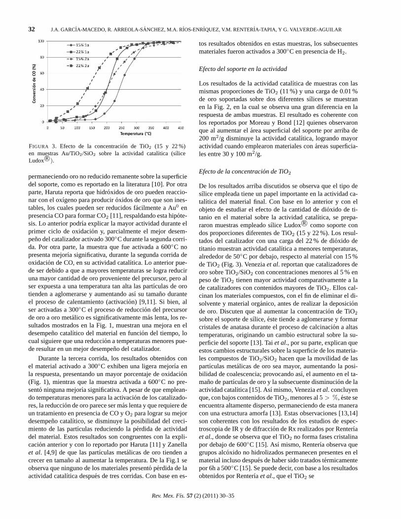
32 J.A.GARCIA-MACEDO, R. ARREOLA-SANCHEZ, M.A. RIOS-ENRIQUEZ, V.M. RENTERIA-TAPIA, Y G. VALVERDE-AGUILAR
FIGURA 3. Efecto de la concentracion de TiO2 (15 y 22 %)en muestras Au/TiO2/SiO2 sobre la actividad catalıtica (sıliceLudox R©).
permaneciendo oro no reducido remanente sobre la superficiedel soporte, como es reportado en la literatura [10]. Por otraparte, Haruta reporta que hidroxidos de oro pueden reaccio-nar con el oxıgeno para produciroxidos de oro que son ines-tables, los cuales pueden ser reducidos facilmente a Au0 enpresencia CO para formar CO2 [11], respaldando esta hipote-sis. Lo anterior podrıa explicar la mayor actividad durante elprimer ciclo de oxidacion y, parcialmente el mejor desem-peno del catalizador activado 300C durante la segunda corri-da. Por otra parte, la muestra que fue activada a 600C nopresenta mejorıa significativa, durante la segunda corrida deoxidacion de CO, en su actividad catalıtica. Lo anterior pue-de ser debido a que a mayores temperaturas se logra reduciruna mayor cantidad de oro proveniente del precursor, pero alser expuesta a una temperatura tan alta las partıculas de orotienden a aglomerarse y aumentando ası su tamano duranteel proceso de calentamiento (activacion) [9,11]. Si bien, alser activadas a 300C el proceso de reduccion del precursorde oro a oro metalico es significativamente mas lenta, los re-sultados mostrados en la Fig. 1, muestran una mejora en eldesempeno catalıtico del material en funcion del tiempo, locual siguiere que una reduccion a temperaturas menores pue-de resultar en un mejor desempeno del catalizador.
Durante la tercera corrida, los resultados obtenidos conel material activado a 300C exhiben una ligera mejorıa enla respuesta, presentando un mayor porcentaje de oxidacion(Fig. 1), mientras que la muestra activada a 600C no pre-sento ninguna mejorıa significativa. A pesar de que emplean-do temperaturas menores para la activacion de los catalizado-res, la reduccion de oro parece ser mas lenta y que requiere deun tratamiento en presencia de CO y O2 para lograr su mejordesempeno catalıtico, se disminuye la posibilidad del creci-miento de las partıculas reduciendo la perdida de actividaddel material. Estos resultados son congruentes con la expli-cacion anterior y con lo reportado por Haruta [11] y Zanellaet al. [4,9] de que las partıculas metalicas de oro tienden acrecer en tamano al aumentar la temperatura. De la Fig.1 seobserva que ninguno de los materiales presento perdida de laactividad catalıtica despues de tres corridas. Con base en es-
tos resultados obtenidos en estas muestras, los subsecuentesmateriales fueron activados a 300C en presencia de H2.
Efecto del soporte en la actividad
Los resultados de la actividad catalıtica de muestras con lasmismas proporciones de TiO2 (11 %) y una carga de 0.01 %de oro soportadas sobre dos diferentes sılices se muestranen la Fig. 2, en la cual se observa una gran diferencia en larespuesta de ambas muestras. El resultado es coherente conlos reportados por Moreau y Bond [12] quienes observaronque al aumentar elarea superficial del soporte por arriba de200 m2/g disminuye la actividad catalıtica, logrando mayoractividad cuando emplearon materiales conareas superficia-les entre 30 y 100 m2/g.
Efecto de la concentracion de TiO2
De los resultados arriba discutidos se observa que el tipo desılice empleada tiene un papel importante en la actividad ca-talıtica del material final. Con base en lo anterior y con elobjeto de estudiar el efecto de la cantidad de dioxido de ti-tanio en el material sobre la actividad catalıtica, se prepa-raron muestras empleado sılice LudoxR© como soporte condos proporciones diferentes de TiO2 (15 y 22 %). Los resul-tados del catalizador con una carga del 22 % de dioxido detitanio muestran actividad catalıtica a menores temperaturas,alrededor de 50C por debajo, respecto al material con 15 %de TiO2 (Fig. 3). Veneziaet al. reportan que catalizadores deoro sobre TiO2/SiO2 con concentraciones menores al 5 % enpeso de TiO2 tienen mayor actividad comparativamente a lade catalizadores con contenidos mayores de TiO2. Ellos cal-cinan los materiales compuestos, con el fin de eliminar el di-solvente y material organico, antes de realizar la deposicionde oro. Discuten que al aumentar la concentracion de TiO2
sobre el soporte de sılice, este tiende a aglomerarse y formarcristales de anatasa durante el proceso de calcinacion a altastemperaturas, originando un cambio estructural sobre la su-perficie del soporte [13]. Taiet al., por su parte, explican queestos cambios estructurales sobre la superficie de los materia-les compuestos de TiO2/SiO2 hacen que la movilidad de laspartıculas metalicas de oro sea mayor, aumentando la posi-bilidad de coalescencia; provocando ası, el aumento en el ta-mano de partıculas de oro y la subsecuente disminucion de laactividad catalıtica [15]. Ası mismo, Veneziaet al. concluyenque, con bajos contenidos de TiO2, menores al5 > %, este seencuentra altamente disperso, permaneciendo de esta maneracon una estructura amorfa [13]. Estas observaciones [13,14]son coherentes con los resultados de los estudios de espec-troscopia de IR y de difraccion de Rx realizados por Renterıaet al., donde se observa que el TiO2 no forma fases cristalinapor debajo de 600C [15]. Ası mismo, Renterıa observa quegrupos alcoxido no hidrolizados permanecen presentes en elmaterial incluso despues de haber sido tratados termicamentepor 6h a 500C [15]. Se puede decir, con base a los resultadosobtenidos por Renterıaet al., que el TiO2 se
Rev. Mex. Fıs. 57 (2) (2011) 30–35

ESTUDIODEL DESEMPENO DE UN CATALIZADOR Au/TiO2/SiO2 EN LA REACCION DE OXIDACION DE CO 33
FIGURA 4. Efecto de la carga de Au (0.01 y 0.002 %) en muestrasde Au/TiO2/SiO2 sobre la actividad catalıtica (sılice LudoxR©).
FIGURA 5. Efecto del numero de corridas sobre la actividad ca-talıtica (sılice LudoxR©).
encuentra con una estructura amorfa incluso en los materialescon contenidos mayores al 20 %, debido a que las muestrasde TiO2/SiO2 no fueron sometidos a temperaturas mayores a150C antes de ser probadas como catalizadores.
Se ha reportado en diversas investigaciones que la acti-vidad catalıtica depende de la carga de oro en los cataliza-dores [11]. Muestras de TiO2/SiO2 al 22 % de TiO2 fuerandepositadas con dos diferentes cargas de Au empleando elmetodo DP-urea [8], los materiales obtenidos fueron emplea-dos durante la oxidacion de CO y como se muestra en laFig. 4. Estos dos materiales ya presentan actividad a tem-peratura ambiente. En esta figura es claro que al disminuirla carga de oro en un 80 % la actividad catalıtica mejora, lo-grando una conversion de CO del 50 % durante la segundacorrida aproximadamente a los 138C en comparacion con elmaterial con una carga de oro de 0.01 % que alcanzo la mismaconversion alrededor de los 255C, es decir, 117C por en-cima de la anterior. La disminucion en la actividad catalıticaesta relacionada con el aumento en el tamano de las partıculasde oro sobre el catalizador, al aumentar la carga de oro, auna-do a que el oro se deposita preferentemente sobre el dioxidode titanio y no sobre la sılice [13], aumentando la posibili-dad de crecimiento de las partıculas. La Fig. 6a muestra unamicrografıa de contraste Z, realizada mediante microscopica
electronica de transmision (TEM) de alta resolucion, en ellase ve claramente como una partıcula de oro se deposito sobreun pequeno casquete de TiO2 que crecio sobre una partıculade sılice LudoxR©.
Esta bien documentado que el tamano de las partıculasmetalicas es de suma importancia en la actividad catalıticade los catalizadores de oro [11] yeste aumenta al someter elcatalizador a altas temperaturas o con su empleo en la oxida-cion de CO [4,9,11]. La muestra con una concentracion del22 % de TiO2 y una carga de 0.01 % de oro fue sometida a 2corridas adicionales en un periodo de 5 dıas. Se observa en laFig. 5 un desplazamiento hacia temperaturas mas altas en la
FIGURA 6. a) b)Micrografıa de contraste Z de muestras de nano-partıculas de oro depositadas sobre TiO2/SiO2; concentracion deoro de 0.01 %.
Rev. Mex. Fıs. 57 (2) (2011) 30–35

34 J.A.GARCIA-MACEDO, R. ARREOLA-SANCHEZ, M.A. RIOS-ENRIQUEZ, V.M. RENTERIA-TAPIA, Y G. VALVERDE-AGUILAR
FIGURA 7. a) Micrografıa de una nano partıcula de oro tomada porTEM. b) Espectro de dispersion de energıa (EDS) realizado en elTEM sobre la nanopartıcula de oro.
tercera y cuarta corrida, de 49 y 58C al 50 % de conver-sion, respectivamente; es decir, una disminucion en la acti-vidad catalıtica debido, presumiblemente, al crecimiento delas partıculas de oro. Comottiet al., prepararon catalizado-res de Au/TiO2 partiendo de una suspension coloidal de oroempleando alcohol polivinılico o glucosa monohidratada co-mo agentes protectores de los coloides. Ellos observan queestos catalizadores mejoran su actividad catalıtica despuesde varias corridas de oxidacion de CO y, que a partir de lacuarta corrida se observa una caıda en la actividad catalıti-ca [16]. Estas observaciones coinciden con el comportamien-to de nuestro catalizador. Comotti explica que, esta mejorıaen la respuesta catalıtica se debe a que el catalizador requie-re de un tratamiento termico mas prolongado en presencia deoxıgeno, esto con el fin de eliminar los agentes protectoresque tienen un efecto inhibitorio en la reaccion y, para lograrla maxima activacion del catalizador [16]. Porultimo, reali-
zan tratamientos termicos a diferentes temperaturas y obser-van que cuando se calientan los catalizadores por arriba delos 400C las perdidas en la actividad catalıtica son mayo-res. Los estudios de espectrofotometrıa de IR de Renterıa etal. [15] revelan la presencia de grupos alcoxido no hidroli-zados que permanecen sobre el sobre el soporte de Au/TiO2.Estos grupos normalmente son eliminados por calcinacion atemperaturas arriba de los 500C, con la consecuente mo-dificacion estructural el TiO2 para formar cristales de ana-tasa [13,14]. Estos grupos alcoxido persistentes en nuestrosmateriales pueden actuar como inhibidores de la reaccionde CO y ser eliminados paulatinamente en presencia de O2
para que la actividad catalıtica mejore durante las primerascorridas como se observa en la Fig. 5. El decaimiento clara-mente marcado de la actividad catalıtica, a partir de la terce-ra corrida, tiene explicacion en el hecho de que estos mate-riales durante las corridas catalıticas fueron calentados hastalos 550C en cada una de ellas, lo cual coincide con los resul-tados reportados por Comottiet al. [16]. Lo anterior suponeuna explicacion alternativa y complementaria del desplaza-miento de las cuervas hacıa temperaturas mas bajas.
Se plantean realizar analisis termogravimetricos y termi-co diferencial para obtener datos que expliquen a detalle estecomportamiento.
Cabe destacar que, los resultados obtenidos en estas dosultimas corridas son muy similares, las curvas se superponenalrededor del 60 % de conversion y la diferencia de tempera-tura entre la tercera y cuarta corrida al 50 % es de solo 9Cdespues de 3 dıas, es decir, la perdida de actividad es muchomenor, lo cual indica que el material tiende a ser estable. De-bido al deposito de dioxido de titanio sobre sılice LudoxR© ya que la carga de oro es muy baja, la dispersion de oro en elmaterial no es homogenea (Fig. 6b).
De acuerdo al analisis quımico hecho por TEM-EDS, lacomposicion de la partıcula mostrada en la Fig. 7, contieneoro, titanio, silicio y oxıgeno, los cuales corresponden al ma-terial Au/TiO2/SiO2, las senales de cobre corresponden a larejilla en la cual esta montada la muestra.
4. ConclusionesEl desempeno, medido como actividad catalıtica, de materia-les compuestos de TiO2/SiO2, es sensible a parametros comoel contenido de TiO2, contenido de oro, tipo de SiO2 que seemplea, metodo de deposicion de las nanopartıculas de oroy la temperatura de activacion de los mismos. Con base enlos resultados obtenidos durante el estudio, se logro mejorarla actividad del catalizador consiguiendo actividad a tempe-ratura ambiente y estabilidad en los materiales durante 5 dıasdespues de 4 corridas de conversion de CO.
AgradecimientoLos autores agradecen el apoyo financiero de los proyec-tos: CONACYT 79781, NSF-CONACYT, PUNTA, PAPIITIN107510 y al ICyT-DF. M. A. Rıos-Enrıquez y GVA agra-decen al ICyT-DF por la Beca posdoctoral.
Rev. Mex. Fıs. 57 (2) (2011) 30–35

ESTUDIODEL DESEMPENO DE UN CATALIZADOR Au/TiO2/SiO2 EN LA REACCION DE OXIDACION DE CO 35
1. G.Cocoet al., J. Phy. Chem.83 (1979) 2527; G.B. Bondet al.,J. Chem. Soc. Chem.Commun.(1973) 444.
2. M. Harutaet al., J. Catal.115(1989) 301.
3. Moreauet al., J. Catal.231(2005) 105.
4. R. Zanellaet al., J. Catal.222(2004) 357.
5. K. Qianet al., J. Catal.248(2007) 137.
6. M.S. Chen y D.W. Goodman,Science306 (2004) 252; N. Lo-pezet al., J. Catal. 23 (2004) 232; M.M. Schubertet al., J. Ca-tal. 197(2001) 113; M. Khoudiakovet al., J. Catal. 291(2005)151.
7. Veneziaet al., Appl. Catal. A310(2006) 114.
8. B. Schumakeret al., Catal. Lett.89 (2003) 109; B.K. Min,etal., J. Phys. Chem. B108(2004) 14609.
9. R. Zanellaet al., J. Phys. Chem. B106(2002) 7634.
10. O. Muller et al., J. Inorg. Nucl. Chem31 (1969) 2966; Green-wood, N. Norman, A. Earnshaw,Chemistry of the Elements(2a Ed.), (Oxford: Butterworth-Heinemann. Woburn, Massa-chusetts, EE.UU.1997)
11. M. HarutaCatal., Today36 (1997) 153.
12. Moreau y Bond,Catal. Today122(2007) 215.
13. M. Veneziaet al., App. Catal. A310(2006) 114; W. Yanet al.,J. Phys. Chem. B109(2005) 15489
14. Y. Tai et al., Appl. Catal. A268(2004) 183.
15. V.M. Renterıa et al., (2010) en preparacion.
16. M. Comottiet al., J. Am. Chem. Soc.128(2006) 917.
Rev. Mex. Fıs. 57 (2) (2011) 30–35

REVISTA MEXICANA DE FISICA S57 (2) 36–40 ABRIL 2011
Photocatalytic activity in the visible region of high energy milledTiO 2:N nanopowders
L. Rojas-Blanco, F.J. Espinoza-Beltran, P.G. Mani-Gonzalez and R. Ramırez-BonCentro de Investigacion y Estudios Avanzados del IPN. Unidad Queretaro,
apartado postal 1-798, Queretaro, Qro., 76001, Mexico,e-mails: [email protected];[email protected];
[email protected]; [email protected]
G. ZambranoThin Films Group,
Universidad del Valle, Cali, Colombia,e-mail: [email protected]
J. Velasquez-SalazarDepartamento de Fısica de la Universidad de Austin Texas,
University Station C1600 Austin, Texas,e-mail: [email protected]
Recibido el 26 de febrero de 2009; aceptado el 16 de julio de 2010
In this work, TiO2:N nanopowders were synthesized by high-energy ball milling using commercial titanium dioxide (TiO2) in the anatasecrystalline phase and urea to introduce nitrogen into the TiO2 lattice in order to enhance their photocatalytic properties in the visible spectralregion. Several samples were prepared by milling a mixture of TiO2-urea powders during 2, 4, 8, 12 and 24 hours and characterized byspectroscopic and analytical techniques. X-ray diffraction (XRD) results showed the coexistence of anatase and the high-pressure srilankiteTiO2 crystalline phases in the samples. Scanning electron microscopy (SEM) revealed that the grain size of the powder samples decreasesto about 200 nm after 24 h of milling. UV–Vis diffuse reflectance spectroscopy measurement showed a clear red-shift in the onset of lightabsorption from about 390 to 470 nm as consequence of nitrogen doping in the samples. The photocatalytic activity of the TiO2:N sampleswas evaluated by methylene blue degradation under visible light irradiation. We found that all samples have a higher photocatalytic activitythan the undoped TiO2, which can be attributed to the effect of the introduction of N atoms into the TiO2 lattice. X-ray photoelectronspectroscopy (XPS) measurements were performed to confirm the presence of N and determine its chemical bonding in the samples.
Keywords:Photocatalysis; titanium oxide; nitrogen doping; srilankite.
En este trabajo, nanopolvos de TiO2:N fueron sintetizados en un molino de bolas de alta energıa usando dioxido de titanio comercial (TiO2)en fase cristalina anatasa y urea para introducir nitrogeno en la red de TiO2 con el objetivo de optimizar sus propiedades fotocatalıticas enla region espectral visible. Varias muestras fueron preparadas moliendo una mezcla de TiO2-urea en polvo durante 2, 4, 8, 12 y 24 horas ycaracterizadas por tecnicas espectroscopicas y analıticas. Los resultados de difraccion de rayos X (DRX) mostraron la coexistencia de lasfases cristalinas anatasa y srilankita de alta presion de TiO2. La microscopıa electronica de barrido (MEB) revelo que el tamano de granodecrece a alrededor de 200 nm despues de 24 horas de molienda. Los datos de espectroscopia por reflectancia difusa en el UV-Vis mostraronun corrimiento en el borde de absorcion de 390 a 470 nm debido a la introduccion de nitrogeno en las muestras. La actividad fotocatalıticade las muestras de TiO2:N fue evaluada por la degradacion del azul de metileno bajo irradiacion de luz visible. Encontramos que todaslas muestras tienen una actividad fotocatalıtica mas alta que las del TiO2 sin dopar, lo cual puede ser atribuido al efecto de la introducciondeatomos de N. Se realizaron tambien mediciones de espectroscopıa de electrones fotoemitidos por rayos X para confirmar la presencia yenlace quımico de losatomos de N en las muestras.
Descriptores:Fotocatalisis; oxido de titanio; dopaje con nitrogeno; srilankita.
PACS: 82.30.Vy; 82.45.Jn; 81.07.Wx; 82.80.Pv
1. Introduction
Heterogeneous photocatalysis of organic compounds onsemiconductor surfaces in aqueous media is an efficientmethod for waste water treatment and its use has been in-creased in recent years [1]. TiO2is a low-cost photocatalystand is the most extensively investigated material in this field.However, its high energy band gap (3.3 eV for anatase phase)limits the photocatalytic process to irradiation wavelengthsin the UV region (λ <390 nm). Such radiation corresponds
to only 5% of the incident solar flux. Due to this limita-tion, the preparation of new photocatalysts which can be ex-cited in the visible range is a currently topic of great inter-est among researchers in the area. One approach is to dopethe TiO2 lattice with transition metals [2] and another one isto form coupled photocatalysts [3]. However, doped mate-rials suffer from thermal instability and increase in carrier-recombination centers. On the other hand, coupled photocat-alysts can efficiently separate photogenerated electron–holepairs, but they are not effective in extending the wavelength
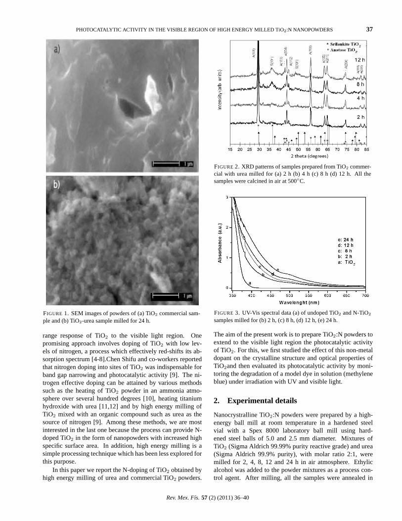
PHOTOCATALYTIC ACTIVITY IN THE VISIBLE REGION OF HIGH ENERGY MILLED TiO2:N NANOPOWDERS 37
FIGURE 1. SEM images of powders of (a) TiO2 commercial sam-ple and (b) TiO2-urea sample milled for 24 h.
range response of TiO2 to the visible light region. Onepromising approach involves doping of TiO2 with low lev-els of nitrogen, a process which effectively red-shifts its ab-sorption spectrum [4-8].Chen Shifu and co-workers reportedthat nitrogen doping into sites of TiO2 was indispensable forband gap narrowing and photocatalytic activity [9]. The ni-trogen effective doping can be attained by various methodssuch as the heating of TiO2 powder in an ammonia atmo-sphere over several hundred degrees [10], heating titaniumhydroxide with urea [11,12] and by high energy milling ofTiO2 mixed with an organic compound such as urea as thesource of nitrogen [9]. Among these methods, we are mostinterested in the last one because the process can provide N-doped TiO2 in the form of nanopowders with increased highspecific surface area. In addition, high energy milling is asimple processing technique which has been less explored forthis purpose.
In this paper we report the N-doping of TiO2 obtained byhigh energy milling of urea and commercial TiO2 powders.
FIGURE 2. XRD patterns of samples prepared from TiO2 commer-cial with urea milled for (a) 2 h (b) 4 h (c) 8 h (d) 12 h. All thesamples were calcined in air at 500C.
FIGURE 3. UV-Vis spectral data (a) of undoped TiO2 and N-TiO2
samples milled for (b) 2 h, (c) 8 h, (d) 12 h, (e) 24 h.
The aim of the present work is to prepare TiO2:N powders toextend to the visible light region the photocatalytic activityof TiO2. For this, we first studied the effect of this non-metaldopant on the crystalline structure and optical properties ofTiO2and then evaluated its photocatalytic activity by moni-toring the degradation of a model dye in solution (methyleneblue) under irradiation with UV and visible light.
2. Experimental details
Nanocrystralline TiO2:N powders were prepared by a high-energy ball mill at room temperature in a hardened steelvial with a Spex 8000 laboratory ball mill using hard-ened steel balls of 5.0 and 2.5 mm diameter. Mixtures ofTiO2 (Sigma Aldrich 99.99% purity reactive grade) and urea(Sigma Aldrich 99.9% purity), with molar ratio 2:1, weremilled for 2, 4, 8, 12 and 24 h in air atmosphere. Ethylicalcohol was added to the powder mixtures as a process con-trol agent. After milling, all the samples were annealed in
Rev. Mex. Fıs. 57 (2) (2011) 36–40

38 L. ROJAS-BLANCO et al.,
air at 500C for 1.0 h. X-ray diffraction measurement ofthe powder samples with different milling times were per-formed using Co-Kαradiation in a Rigaku D/max-2100 X-ray diffractometer. The morphology of TiO2 milled parti-cles was observed by scanning electron microscopy (SEM)with a Philips XL30-SEM instrument. In the photocatalyticactivity experiments, the TiO2:N powders were placed intoa methylene blue solution (concentration 15 mg/l), in orderto study the kinetic of its degradation as function of the ex-posure time to the visible light irradiation from a tungstenhalogen lamp. Firstly, the powdered samples (about 200 mg)were dispersed into 200 ml of methylene blue aqueous solu-tion (Ci=15 mg/L) stirring magnetically for 30 min to estab-lish absorption/desorption equilibrium. After the suspensionswere centrifuged at 2000 rpm, the concentrations (C0) of the
FIGURE 4. XPS survey of the sample milled for with 24 hr wherethe signal of O 1s, Ti 2p C1s are observed. The N1s signal is veryweak.
FIGURE 5. XPS spectra in the O1s region of samples milled for(a) 24 h and (b) 4 h with urea.
FIGURE 6. XPS spectra in the Ti2p region of samples milled for:(a) 24 h and (b) 4 h with urea.
FIGURE 7. XPS spectra in the N1s region of samples milled for:(a) 24 h and (b) 4 h with urea.
FIGURE 8. Photocatalytic degradation of methylene blue dye inthe presence of N-doped TiO2 nanoparticles.
Rev. Mex. Fıs. 57 (2) (2011) 36–40

PHOTOCATALYTIC ACTIVITY IN THE VISIBLE REGION OF HIGH ENERGY MILLED TiO2:N NANOPOWDERS 39
solutions were measured from absorption spectra at 662 nmon a UV–Vis spectrometer. Then, the tungsten halogen lampwas switched on, and the aqueous suspensions containingmethylene blue and powdered catalysts were irradiated. Atthe given time intervals, 5 ml of the suspension were takenfrom the suspensions and their concentrations were mea-sured. The XPS (X-ray Photoelectron Spectroscopy) datawere obtained using a ThermoElectron instrument with aXPS110 electron analyzer employing non-monocromatic AlKα X-ray (hν=1486.6 eV) at 100 W with an electron take-off angle of 90. Samples were attached on top of a sampleholder by Indium foil. The spectrometer is equipped with aseven-channel hemispherical detector. The lens mode usedwere small area XPS 600µm with slit 0 and aperture 4. Passenergy of 100 eV for surveys and 50 eV for high resolutionwere used during the analysis of the samples. The scan num-bers were different for each range of core level electron en-ergy states of samples. All analyses were performed at a vac-uum pressure of 3 x 10⁻¹⁰ Torr. XPS measurements providedinformation regarding the form which nitrogen is bonding inthe TiO2 lattice. The XPS peaks were fitted into subcompo-nents using the software Aanalyzer [13].
3. Results and discussion
Figure 1 shows the SEM images of (a) unmilled TiO2 sampleand b) 24 hours milled TiO2 sample. The unmilled sampleshows a microstructure of irregularly shaped laminar crystals,meanwhile the milled sample shows agglomerated nanopar-ticles with an average size of about 200 nm. These imagesshow clearly the effect of high energy milling on the parti-cle size of TiO2. The XRD patterns of the milled samplesare shown in Fig. 2. At the bottom are indicated the po-sitions of the diffraction peaks of the anatase (JCPDS#00-021-1272) and srilankite (JCPDS #00-035-0584) phases ofTiO2. The evolution of these patterns with milling time indi-cates that ball milling induces the crystalline phase transfor-mation from tetragonal anatase to orthorhombic srilankite inthe TiO2 powders. It has been shown that the milling-inducedtransformation from anatase to srilankite in nanocrystallineTiO2 is partly attributed to the rise of the local temperatureand pressure at the collision sites of the powder and the balls.However, it can also be seen in this figure that not all anatasephase transforms into srilankite one, because the presence ofanatase diffraction peaks in the milled samples patterns.
Figure 3 shows the UV-Vis absorption spectra of undopedand nitrogen-doped TiO2samples. These data reveal that ni-trogen doping of TiO2 nanoparticles shifts the absorptionedge toward higher wavelength from about 390 to 470 nm,that is toward the visible region with a substantially long bandtailing produced by dopant-defect states. From these spectra,the mean band gap values were found to be 3.2 and 2.64 eVfor undoped and doped samples, respectively.
XPS measurements provided information about the incor-poration of N into TiO2 powders after high energy millingprocessing. Figure 4 shows the XPS survey scan of the
TiO2:N sample milled for 24 hours where the signals of O1s,Ti 2p, N 1s and C1s can be observed. High resolution XPSscans were performed to identify the chemical bonding of O,Ti and N in the milled samples. The O1s region displayeda signal with peaks (Fig. 5) in 540.4, 539.4 and 538.2 eVcorresponding to Ti-O and C-O bonding and O1s, respec-tively. The XPS spectrum (Fig. 6) in the Ti2p region showedthe doublet2p1/2(472.6 eV) and2p3/2 (467 eV) of titanium.The signals of titanium oxide, titanium nitride and titaniumcarbide in 468.4, 469.9 and 471.1 eV, respectively, were iden-tified in this spectrum. Figure 7 shows the XPS results in theN 1s region for the unmilled sample and milled samples for4 and 24 h. The N1s peak at 408.5 eV corresponds to N inthe N-Ti bond indicating that N atoms substitute O atoms inthe TiO2 lattice. This peak is more intense in the spectrumof the sample milled for 4 h than in the one of the samplemilled for 24 h. It indicates that the former sample has alarger amount of nitrogen at the surface. This difference canbe explained in terms of thermal stability of the TiO2:N pow-der. After few hours of milling, urea compound is destroyedand a small amount of nitrogen from urea diffuses into TiO2
crystals. For higher milling times, above 4 hours, N-dopedTiO2 powder is kept at temperatures about 80C or higher.At this temperature TiO2:N powder could be unstable losingits nitrogen content. The previous results show that N waseffectively introduced into the TiO2 lattice after high energymilling of the mixture of TiO2-urea powders. In addition,the N-doping enhanced the optical absorption of TiO2 in thevisible light region.
In order to study the effect of N-doping on the catalyticproperties of TiO2, the catalytic activities of the nanopow-der samples were estimated by the degradation of methyleneblue in solution after exposure to irradiation. Figure 8 showsthe methylene blue solution absorption spectra after differ-ent times of exposure to lamp irradiation as described in theexperimental section. The spectrum of the solution beforelight exposure displays the typical methylene blue absorptionbands at about 600 and 660 nm. The decrease in the intensityof these absorption bands is due to the photodegradation ofmethylene blue in the presence of N-doped TiO2 nanoparti-cles of the sample milled for 24 h. Thus, the results in Fig. 8,clearly show a significant decrease in the absorption bands in-tensity of methylene blue, indicating substantial degradationof the dye under the visible light dominated illumination.
4. ConclusionsIn conclusion we found that N-doped anatase titania couldbe prepared by a high energy ball mill using titanium ox-ide commercial and urea. The substitutional N doping ofTiO2 broaden the light absorption spectrum to the visible re-gion to make it visible light active. XPS measurements con-firmed the incorporation of N atoms substituting O atoms inthe crystalline lattice of TiO2.The photocatalytic activity ofTiO2:N samples induced by visible light was corroboratedby the methylene blue photodegradation in our photocatalyticexperiments.
Rev. Mex. Fıs. 57 (2) (2011) 36–40

40 L. ROJAS-BLANCO et al.,
Acknowledgements
The helpful technical assistance of J.E. Urbina Alvarez andM.A. Hernandez Landaverde is acknowledged.
1. C.J.Tristao, F. Magalhaes, P. Corio, and C.M.E. Sansiviero,J.Photochem and Photobiol.181(2006) 152.
2. K. Lee, N.H. Lee, S.H. Shin, H.G. Lee and S.J. Kim,MaterialsScience and Engineering: B.129(2006) 109.
3. Y. Bessekhouadet al., Journal of Photochemistry and Photobi-ology A: Chemistry183(2006) 218.
4. R. Asahi, T. Morikawa, T. Ohwaki, K. Aoki, and Y. Taga,Sci-ence, 293(2001) 269.
5. S. Sakthivel, M. Janczarek, and H. Kisch,J. Phys. Chem. B.108(2004) 19384.
6. S. Sakthivel and H. Kisch,Chem. Phys. Chem.4 (2003) 487.
7. K. Kobayakawa, Y. Murakami and Y. Sato,J. Photochem. Pho-tobiol. A170(2005) 177.
8. Z.P. Wanget al., Appl. Catal. B57223 (2005).
9. Chen Shifu, Chen Lei, Gao Shen, and Cao Gengyu,ChemicalPhysics Letters413(2005) 404.
10. H. Irie, Y. Watanabe, and K. Hashimoto,J. Phys. Chem. B107(2003) 5483.
11. JianYuan, Mingxia Chen, Jianwei Shi, and Wenfeng Shang-guan. International Journal of Hydrogen Energy31 (2006)1326.
12. K. Kobayakawa, Y. Murakami, and Y. Sato.Journal of Photo-chemistry and Photobiology A: Chemistry170(2005) 177.
13. A. Herrera-Gomez, “Analyzer: An Analysis Software for Pho-toelectron and Infrared Spectra”.
Rev. Mex. Fıs. 57 (2) (2011) 36–40

REVISTA MEXICANA DE FISICA S57 (2) 41–43 ABRIL 2011
Preparacion de nanoparticulas polimericas con aplicacion farmaceuticausando tecnicas basadas en emulsificacion
N. Naranjos-Ramırez, D.I. Torres-Cantu, V.I. Castillo-Rodrıguez, S.A. Galindo-Rodrıguez y A. Chavez-MontesDepartamento de Quımica, Facultad de Ciencias Biologicas, Universidad Autonoma de Nuevo Leon,
Av. Manuel L. Barragan s/n Cd. Universitaria 66451, Monterrey, N.L. Mexico,e-mail: [email protected]
R. Castro-Rıos y R.Alvarez-RomanDepartamento de Quımica Analıtica, Facultad de Medicina, Universidad Autonoma de Nuevo Leon,
Av. Madero y Dr. Aguirre Pequeno Col. Mitras Centro 64460. Monterrey, N.L. Mexico,e-mail: roc alvarez [email protected]
M.E. Martınez-BarbosaDepartamento de Investigacion en Polımeros y Materiales, Universidad de Sonora,
Blvd. Rosales y Luis Encinas s/n 83000, Hermosillo, Sonora, Mexico,e-mail: [email protected]
Recibido el 29 de enero de 2010; aceptado el 13 de julio de 2010
Desde el punto de vista farmaceutico, el tamano de las nanopartıculas polimericas (NP) es un parametro clave en su interaccion con sistemasbiologicos. El objetivo de este estudio fue establecer la influencia de la velocidad de homogenizacion, la concentracion de agente tensoactivo yla relacion de fase organica/fase acuosa sobre el tamano de NP preparadas mediante los siguientes metodos de emulsificacion: doble emulsion(w/o/w)-evaporacion, emulsificacion-evaporacion y emulsificacion-difusion. Las NP fueron formadas a partir de polımeros derivados deacido metracrılico. Polivinilalcohol (PVA) y Lutrol F127 (Poloxamer) fueron usados como tensoactivos. Las tecnicas permitieron obtenerpartıculas con tamanos definidos de 182 a 545 nm.
Descriptores:Nanopartıculas polimericas; fabricacion de nanopartıculas; caracterizacion de nanopartıculas.
From pharmaceutical point of view polymeric nanoparticle (NP) size is a key interaction parameter with biological systems. The aim ofthis study was to establish the influence of stirring rate, surfactant concentration and organic phase/aqueous phase ratio on the size of NPprepared by double emulsion (w/o/w)-evaporation, emulsification-evaporation and emulsification-diffusion methods. Polymers derived frommethacrylic acid were used to form the NP and polyvinylalcohol (PVA) and Lutrol F127 (Poloxamer) were used as surfactants. The evaluatedexperimental parameters allow to obtain NP with defined size from 182 to 545 nm.
Keywords: Polymeric nanoparticles; fabrication of nanoparticles; characterization of nanoparticles.
PACS: 81.07.-b; 81.16.-c
1. Introduccion
Durante lasultimas decadas, las nanopartıculas polimeri-cas (NP) han sido ampliamente investigadas en elarea far-maceutica como sistemas de liberacion de principios activos,principalmente, debido a que pueden mejorar la estabilidad,la biodisponibilidad y el direccionamiento de farmacos a unsitio blanco [1]. Asimismo, las NP ofrecen ventajas como po-tenciar la absorcion del farmaco en el tejido diana, reducirlos efectos adversos y disminuir la dosificacion. Una de lascaracterısticas mas significativas de las NP es el tamano, yaque facilita la entrada y mejora la interaccion deestas conlos sustratos biologicos (i.e.celula o tejido). La obtencion deNP con tamano definido se logra, basicamente, modificandodistintas variables experimentales del metodo utilizado parapreparar a las NP. Entre los metodos mas comunmente usa-dos para obtener NP se encuentran aquellos basados en laformacion de una emulsion [2]. En el presente estudio, seevaluaron los principales parametros que influyen en el ta-mano de NP preparadas mediante tres tecnicas: emulsifica-cion-difusion, emulsificacion-evaporacion y doble emulsion
(w/o/w)-evaporacion. En elarea farmaceutica, las dos prime-ras tecnicas son utilizadas para incorporar principios activoshidrofobicos, mientras que, laultima es empleada para incor-porar farmacos hidrofılicos.
2. Materiales y metodos
2.1. Materiales
Alcohol polivinılico (PVA, Mowiol R© 4-88) fue donado ama-blemente por Clariant Mexico. LutrolR© F127 (Poloxamer407) fue donado gentilmente por BASF Mexico. Los polıme-ros derivados de metacrilato EudragitR© E100, EudragitR©L100 55 y EudragitR© RL100 fueron gentilmente donadospor Helm Mexico. El resto de los reactivos empleados fueronde grado reactivo.
2.2. Preparacion de las nanopartıculas polimericas
Las nanopartıculas fueron preparadas de acuerdo a los pro-cedimientos de las tecnicas emulsificacion-difusion, emulsi-ficacion-evaporacion y doble emulsion (w/o/w)-evaporacion.

42 N. NARANJOS-RAMIREZ et al.,
FIGURA 1. Relacion del diametro de nanopartıcula en fun-cion de la concentracion de tensoactivo en las tecnicas de A)Emulsificacion-difusion B) Emulsificacion-evaporacion C) Dobleemulsion (w/o/w)-evaporacion (n= 3).
Emulsificacion-difusion.2.1 g de fase organica, que con-tiene el polımero formador de las nanopartıculas (500 mgde Eudragit L100-55) en 9.5 mL de alcohol bencılico, seemulsionan agitando a 2000 rpm (Eurostar Power-b, IKA-WERKE) con 3.0 g de una fase acuosa que contiene PVA al14 % (p/p). A la emulsion resultante se le adicionaron 66 g deagua destilada para inducir tanto la difusion del solvente de lafase organica a la fase acuosa, como la formacion de las NP.
Emulsificacion-evaporacion. 10 g de una fase organicaconstituida de Eudragit E100 (500 mg) disuelto en acetato deetilo fue adicionada a 20 g de una fase acuosa de Poloxameral 4 % (p/v). La emulsificacion de las dos fases se realizo a2000 rpm (Eurostar Power-b, IKA-WERKE), seguida de unahomogenizacion (7,900–20,450 rpm) (VDI 12, VWR). Unavez obtenida la emulsion, el solvente se evaporo a presionreducida para inducir la formacion de las NP.
Doble emulsion (w/o/w)-evaporacion.La formacion de laprimera emulsion se obtuvo mezclando con agitacion 1 mLde una fase acuosa interna (agua destilada) con 10 mL de fa-se organica (20 mg de Eudragit RL100 en cloroformo). La
emulsion primaria (w1/o) resultante se adiciono a una faseacuosa externa conteniendo 4 % (p/p) de PVA, manteniendo-se una agitacion constante a 2000 rpm. La emulsion obte-nida (w1/o/w2) fue homogenizada a diferentes velocidades(9,400-20,450 rpm). Finalmente, la evaporacion del solventea presion reducida dio como resultado la formacion de las NP.
Las siguientes variables fueron modificadas para deter-minar su efecto sobre el tamano de nanopartıcula: la con-centracion de tensoactivo en la fase acuosa, la relacion fa-se organica/fase acuosa externa, la velocidad de agitacion yla velocidad de homogenizacion. Cada lote fue realizado portriplicado.
FIGURA 2. Influencia de la relacion fase organica/fase acuosa so-bre el tamano de nanopartıcula en la tecnica de doble emulsion(w/o/w)-evaporacion (n= 3 ).
FIGURA 3. Influencia de la velocidad de homogenizacion sobre eldiametro de nanopartıcula en las tecnicas de A) Emulsificacion-evaporacion y B) Doble emulsion (w/o/w)-evaporacion (n= 3 ).
Rev. Mex. Fıs. 57 (2) (2011) 41–43

PREPARACION DE NANOPARTICULAS POLIMERICAS CON APLICACION FARMACEUTICA USANDO TECNICAS. . . . 43
2.3. Determinacion del tamano de la nanopartıcula
La determinacion del tamano de las NP se realizo por espec-trofotometrıa de correlacion fotonica (Zetasizer Nano ZS90,Malvern Instruments, R.U.) a partir de un alıcuota de cadalote diluida en agua Milli-Q.
3. Resultados y discusion
3.1. Efecto de la concentracion de tensoactivo sobre eltamano de NP
En la tecnica de emulsificacion-difusion se observo que elincremento en la concentracion de tensoactivo (PVA) de 10 a16 % en la fase acuosa disminuyo el tamano de las NP de 400a 182 nm (Fig. 1). Considerando que las cadenas polimeri-cas de PVA que interactuan en la interfase fase organica–faseacuosa reducen la tension interfacial y funcionan como unabarrera mecanica evitando la coalescencia de los globulos du-rante la emulsificacion, un incremento en la concentracion detensoactivo en la fase acuosa permite que haya mas molecu-las deeste en la superficie de los globulos, estabilizandolos yreduciendo su tamano [4]. El mismo comportamiento se ob-servo en la tecnica de emulsificacion-evaporacion, al variarla concentracion de tensoactivo (Poloxamer 407) de 4 a 11 %(p/v) se obtuvieron tamanos de 505 a 378 nm. Un compor-tamiento similar se observo a velocidades de homogeniza-cion de 9,400 a 14,450 rpm. En la tecnica de doble emulsion(w/o/w) la variacion en la concentracion del agente tensoac-tivo (PVA) de 3-6 % (p/p) permitio obtener tamanos de 325 a248 nm (Fig. 1).
3.2. Efecto de la relacion de fase organica/fase acuosaexterna sobre el tamano de NP
En la tecnica de doble emulsion (w/o/w)-evaporacion se ob-servo que un cambio en la relacion fase organica/fase acuosaexterna de 1.7 a 2.5 provoca una disminucion del tamano deNP de 341 a 269 nm (Fig. 2). Es probable que este compor-tamiento se deba a que al aumentar el volumen del solventeorganico las cadenas polimericas se encontraran mas dilui-das en el seno del globulo de emulsion, lo que inducira la
formacion de una NP mas pequena durante la agregacion delpolımero [5].
3.3. Efecto de la velocidad de homogenizacion sobre eltamano de NP
Al aumentar la velocidad de homogenizacion se observo unadisminucion del diametro de NP. Este comportamiento puedeexplicarse si consideramos que el incremento en la veloci-dad de agitacion produce mas turbulencia de la fase continualo que provocan un mayor corte de los globulos de la emul-sion, llevando ası a la reduccion del tamano deestos y enconsecuencia de las NP [6]. En la tecnica de emulsificacion-evaporacion se obtuvieron tamanos de NP de 521 a 250 nmutilizando velocidades de 7,900 a 20,450 rpm. Para la tecni-ca de doble emulsion (w/o/w) se obtuvo un rango de 547-230 nm en el intervalo de velocidades 9,400-20,450 rpm(Fig. 3).
4. Conclusion
Para las tres tecnicas de emulsificacion, la variacion en el ta-mano de NP tuvo una relacion inversamente proporcional ala velocidad de homogenizacion, la relacion de fase organi-ca/fase acuosa y a la concentracion de tensoactivo. Este es-tudio comparativo permite elegir la tecnica adecuada para laformulacion de NP con un tamano de partıcula definido den-tro del rango de 547 a 230 nm.
Agradecimientos
El presente trabajo es apoyado por el Consejo Nacio-nal de Ciencia y Tecnologıa a traves de los proyectosSALUD-2006-C01-45069 y Tutorıa Licenciatura 104554.Asimismo, los autores agradecen el apoyo otorgado porel PROMEP-SEP a traves de los proyectos Nuevos PTCPROMEP/103.5/08/4913 y Red Tematica Tuberculosis PRO-MEP/103.5/09/4935 P/CA-180. El trabajo es tambien apoya-do por el proyecto PAICyT 2009-UANL SA210-09.
1. S.A. Galindo-Rodrıguez, E. Allemann, H. Fessi y E. Doelker.Pharm. Res.21 (2004) 1428.
2. V.J. Mohanraj y Chen.J. Pharm. Res.5 (2006) 561.
3. A. Lamprechtet al., Int. J. Pharm.196(2000) 177.
4. S.K. Sahoo, J. Panyam, S. Pravha y V. Labhasetwar,J. Control.Rel. 82 (2002) 105.
5. A.F. Citalan Madrid,Tesis de licenciatura(U. Aut. Chiapas Me-xico, 2009).
6. N. Rizkalla, Ch. Range, F. Lacasse y P. Hildgen,J. Microencap23 (2006) 39.
Rev. Mex. Fıs. 57 (2) (2011) 41–43

REVISTA MEXICANA DE FISICA S57 (2) 44–50 ABRIL 2011
Push-pull chromophores aggregation in SiO2 sol-gel films doped withsilver nanoparticles
A. Francoa,b,∗, G. Brusatina, M Guglielmia, V. Renteriab, G. Valverde-Aguilarb, and J.A. Garcıa-MacedobaDipartimento di Ingegneria Meccanica (Settore Materiali),
Universita degli Studi di Padova. Via Marzolo 9, 35131, Padova, Italia.bDepartamento de Estado Solido. Instituto de Fısica, Universidad Nacional Autonoma de Mexico,
Mexico D.F. 04510. D.F., Mexico.∗Instituto de Fısica, Universidad Nacional Autonoma de Mexico,
Circuito de la Inv. Cientıfica s/n 04510. Del. Coyoacan Mexico, D.F. Mexico,Tel. (5255) 56225103; Fax (5255) 56225100
e-mails: [email protected]; [email protected]
Recibido el 29 de enero de 2009; aceptado el 14 de julio de 2010
Sol-gel films used for second-order non-linear optical applications often contain some organic molecules working as spacers between chro-mophores with large permanent dipolar moments. The spacers improve the optical quality of the films because they avoid the chromophoresaggregation. We propose the use of silver nanoparticles as good spacers, instead of organic molecules. In this work the effect of silvernanoparticles on the arrangement of push-pull chromophores inside SiO2 sol-gel films is investigated by UV-vis optical absorption spec-troscopy. Key variables for a good performance of spacers are: their polarizability, their concentration with respect to the concentration ofthe chromophores, as well as the temperature of the system. Disperse Red 1 chromophores, well known push-pull chromophores, arrangethemselves forming H-aggregates when they are inside films in high enough concentrations. Those aggregates are clearly detected by UV-visoptical absorption spectroscopy, where they show an absorbance peak close to 404 nm. That peak disappears as the temperature of thefilms and/or the concentration of the spacers and/or the polarizability of the spacers increase. A possible electrostatic shielding betweenthe chromophores, created by the spacers, makes us to think about the possibility to use metallic nanoparticles as a new kind of molecularspacer.
Keywords: Sol-gel films; metallic nanoparticles; molecular aggregation; UV-vis spectroscopy; push-pull chromophores.
Las pelıculas sol-gel empleadas para aplicaciones enoptica no lineal de segundo orden frecuentemente contienen moleculas organicasque funcionan como espaciadores entre cromoforos que tienen momentos dipolares permanentes grandes. Los espaciadores mejoran lacalidadoptica de las pelıculas porque evitan la agregacion de cromoforos. Nosotros proponemos el uso de nanopartıculas de plata comobuenos espaciadores, en vez del uso de moleculas organicas. En este trabajo se investiga el efecto de las nanopartıculas de plata sobre elarreglo de cromoforos push-pull dentro de pelıculas sol-gel de SiO2 por medio de espectroscopia de absorcion optica UV-vis. Las variablesclave para un buen desempeno de los espaciadores son: su polarizabilidad, su concentracion en relacion a la concentracion de cromoforos,ası como la temperatura del sistema. Los cromoforos Disperse Red 1, cromoforos push-pull bien conocidos, se acomodan por sı mismosformando agregados H, cuando se encuentran dentro de pelıculas en concentraciones suficientemente grandes. Tales agregados son detectadosclaramente mediante espectroscopia de absorcion optica UV-vis, en donde exhiben un pico de absorcion cercano a los 404 nm. Dicho picodesaparece conforme la temperatura de las pelıculas y/o la concentracion de los espaciadores y/o la polarizabilidad de los espaciadoresaumentan. Un posible apantallamiento electrostatico entre los cromoforos, creado por los espaciadores, nos hace pensar en la posibilidad deusar nanopartıculas metalicas como un nuevo tipo de espaciador molecular.
Descriptores: Pelıculas sol-gel; nanopartıculas metalicas; agregacion molecular; espectroscopia UV-vis; cromoforos push-pull.
PACS: 78.40.Me; 78.67.Bf
1. Introduction
Sol-gel films doped with organic push-pull chromophores arepotential candidates for photonics applications due to the easeof their fabrication and their good optical performances [1,2].However, they have some features to overcome: the smallamount of chromophores that sol-gel films can host and theirstability. In particular, for second-order non-linear optical ap-plications the stability means to maintain the chromophoresoriented non-centrosymmetrically inside the material. Dueto the fact that push-pull chromophores usually have largepermanent dipolar moments, they tend to form aggregates,in consequence they do not distribute homogeneously in thematerials when their concentration is high. Also, if the chro-
mophores are oriented in a particular way inside a matrix,they tend to loose their orientation because of dipole-dipoleinteractions [3]. For blocking the strong dipole-dipole inter-actions between chromophores it is common to incorporateother kind of organic molecules in the materials, as the car-bazole moieties, in order to increase the quantity and stabilityof the push-pull chromophores inside the materials [4]. Weuse silver nanoparticles as a novel kind of inorganic spacersbetween chromophores.
The existence of surface plasmons in metallic nanoparti-cles indicates that they are highly polarizable moieties, thusthey should be able to block efficiently the interactions be-tween chromophores. It means that metallic nanoparticlesshould be able to avoid the formation of push-pull chro-

PUSH-PULLCHROMOPHORES AGGREGATION IN SiO2 SOL-GEL FILMS DOPED WITH SILVER NANOPARTICLES 45
mophores aggregates and to increase the stability of the chro-mophores orientation.
In this work we present the physical mechanism be-hind the molecular spacers, the synthesis of sol-gel filmsdoped with push-pull chromophores and metallic nanopar-ticles, the detection of surface plasmons and molecular ag-gregated states in the films by means of UV-vis optical ab-sorption spectroscopy, and finally we analyze and discuss theresults.
2. Physical model
When a material has a very low chromophores concentra-tion, the chromophores are homogeneously distributed insidethe material, the distance between them is very large and thedipole-dipole interactions are negligible. Therefore, at lowchromophores concentrations it is not necessary to use spac-ers in order to avoid aggregation. But as the chromophoresconcentration increases in a system, the distance betweenchromophores decreases, the dipole-dipole interactions be-come larger and different kinds of aggregation structures takeplace. Then the use of spacers becomes necessary in order toavoid the aggregation of the chromophores.
Some molecular spacers decrease the dipole-dipoleelectrostatic interactions existing between push-pull chro-mophores by the means of the induction of an electrostaticshielding between neighbor chromophores. It means that thelarge permanent dipole of the push-pull chromophores inducedipoles in the spacers, which screen the interaction betweenthe permanent dipoles of neighbor chromophores.
An induced dipolep in a spacer is directly related to thepolarizability of the spacer←→α and to the external electro-static fieldE in which the spacer is immersed by means ofthe equation:
p = ←→α E (1)
Thus, as the components of the polarizability are larger,the induced dipoles in the spacers should shield better the in-teractions between chromophores.
In general, the polarizability is directly related to the mo-bility of the charge carriers of the spacers; actually, it is easierto induce a dipole in a molecule whose electrons have a largeenough mobility [5]. It suggests that the surface charge car-riers of metallic nanoparticles can shield properly the dipole-dipole interactions between push-pull chromophores.
In a system with both of them, highly polarizable spacerswith a negligible permanent dipole and chromophores withlarge permanent dipoles, the field due to the chromophoresinduce dipoles in the spacers; then besides the dipole-dipoleinteractions, the dipole-induced dipole ones take place in thesystem too. The dipole-induced dipole coupling can occur,turning more difficult the dipole-dipole aggregation of thechromophores. In consequence, materials doped with highlypolarizable spacers increase the amount of non-self-coupledpush-pull chromophores that they can host.
FIGURE 1. Scheme about how the polarization of the spacers helpsto avoid the chromophores aggregation and to improve the chro-mophores alignment stability through an electrostatic shielding.
Rev. Mex. Fıs. 57 (2) (2011) 44–50

46 A. FRANCOet al.
FIGURE 2. Schematic picture with the two cases considered fromthe Onsagers theory. (a) Polarizable shell inside a constant electricfield. (b) Polarizable shell with a permanent dipole at its center.
This kind of highly polarizable spacer-chromophore sys-tem is attractive too for those materials in which their chro-mophores are oriented non-centrosymmetrically with the useof an external intense electrostatic field, because the ex-ternal field also induces a dipole in the spacers, breakingany kind of zero dipolar moment formed in dipole-induceddipoles structures. Besides, when the external field is off,the chromophores are again the main responsible of the in-duced dipoles in the spacers, but now the induced dipoles arenon-centrosymmetrically oriented too, which helps to main-tain the particular orientation of the chromophores,i.e. it in-creases the stability of the system. The scheme in Fig. 1exemplifies the situation.
Summarizing, the spacer works in two different ways: (a)as a physical spacer, increasing the distance between chro-mophores, and (b) as an electrostatic screen, shielding theelectrostatic interactions between chromophores. In any case,the effect of a spacer should be stronger as its polarizabilityis larger.
In order to understand better the effect of the polariz-able spacers on the chromophore-chromophore interactionswe have taken into account an extension of the well knownOnsagers theory for polarizable media [6].
We assume, as an approximation, that the molecular spac-ers modify in a continuous way the surrounding medium ofeach chromophore. We describe this surrounding medium bya spherical shell made mainly by spacers, with aε2 dielectricconstant, different from the dielectric constants correspond-ing to that of the outside shell medium made by the support-ing matrix (ε3), and to that of the inside medium, where achromophore can be hosted (ε1). It is reasonable to considerε1 ≈1 in those materials plenty of free volume cavities wherechromophores can be hosted; that is the case of some poly-meric or SiO2 sol- gel films [7,8].
Also, it is plausible to assume that the shell itself obeysthe Clausius-Mossotti relation,i.e., the dielectric constant ofthe shell is related to the densityN and to the polarizabilityof the spacers by means of the equation:
ε2 − 1ε2 + 2
=Nα
3. (2)
Two different situations are considered. In first place, asdepicted in Fig. 2a, a system immersed in a constant elec-trostatic field; this situation is analogous to have a film im-mersed in an external electrostatic field. The field inside the
FIGURE 3. (a)E1/E0 vs. Nα plot. (b)E3/Edipole vs. Nαglot.
shell is the field that a chromophore can experience; that fieldcan eventually orient the chromophore in a particular direc-tion. In second place, as depicted in Fig. 2b, a system withoutthe influence of an external field, but with a dipole situatedat the center of the shell; from this situation the field thatanother chromophore experiences outside the shell is deter-mined.
After considering usual boundary conditions of continu-ity of the electrostatic potential and continuity of the elec-tric displacement field between two adjacent media, follow-ing the procedure suggested by E. Riandeet al., [6] and On-sager [9], assuming that spacer molecules form a continuousshell that obeys Clausius-Mossotti relation and encloses anempty cavity, the results in terms of electric fields are: Forthe first case (a), inside the shell there is an electrostatic fieldwith the same direction of the external field and with a con-stant magnitude everywhere. The ratio between the magni-tudes of the electric field inside (E1) and outside (E0) theshell is given in the next equation
E1
E0=
9ε3 (2Nα + 1)(2ε3 + 2Nα + 1) (4Nα + 3)
(3)
For the second case (b), the ratio between the magnitudesof the electrostatic field outside the shellE3, when a perma-nent dipole is at the center of the shell, and the electrostaticfield of the simple situation of a dipole in vacuumEdipole is,everywhere:
E3
Edipole=
9 (2Nα + 1)(2ε3 + 2Nα + 1) (4Nα + 3)
. (4)
A plot of Eqs. (3) and (4) are shown in Fig. 3. In thecase (a), the plot compares, as a function ofNα, the electricfield magnitude in the region inside the polarizable shell (sys-tem with spacers) with respect to the electric field magnitudein the same region but without a polarizable shell,i.e. whenε2=1 (system without spacers).
In case (b), the comparison is done between the mag-nitude of the electric field produced outside the polarizableshell by the dipole (system with spacers), and the magnitude
Rev. Mex. Fıs. 57 (2) (2011) 44–50

PUSH-PULLCHROMOPHORES AGGREGATION IN SiO2 SOL-GEL FILMS DOPED WITH SILVER NANOPARTICLES 47
of the electric field produced by the dipole when it is in vac-uum,i.e. ε1=ε2=ε3= 1 (system without spacers).
Note that the plots are not 1 atNα equal to zero, becauseatNα equal to zero the equations still consider two differentregions: supporting matrix and vacuum.
In Eq. (3) there are not spatial variables, it means that adipole inside the shell experiences a spatially constant field,with the same direction of the external one; and for fewNαvalues, the field is even larger in magnitude. As the polariz-ability of the spacers and/or their concentration increase, themagnitude of the field inside the shell diminishes.
On the other hand, the field due to a fixed dipole in-side the shell is always lower outside, with respect to thefield produced by the dipole in the absence of the spacers(E3/Edipole <1). This field decreases its magnitude as thenumber of spacers and/or their polarizability increase.
All this means that spacers with large enough polariz-abilities and negligible permanent dipole moments, in an ap-propriate concentration inside a material which hosts chro-mophores (SiO2 is the hosting material in this work), de-crease the dipole-dipole interactions between neighbor chro-mophores, but they still allow the molecular orientation bymeans of an external electric field. From this point of view,these spacers increase the stability of those materials whichrequire a particular orientation of their chromophores.
This spherical shell model is a simplification of the realsituation, but it clarifies the processes behind the influencethat polarizable spacers exert on dipole-dipole chromophoresinteractions, even if the model is based on the assumption of amacroscopic, continuous and isotropic behavior of the media,which obeys the Clausius-Mossotti relation. In real materialsthere is a discrete ratio between the number of chromophoresand the number of spacers.
Thus, highly polarizable nanoparticles, like silvernanoparticles, are good candidates to work well as molecu-lar spacers.
3. Experimental details
In order to study how metallic nanoparticles influence push-pull chromophores aggregation in a real system, hybrid SiO2
films doped with both, push-pull chromophores and silvernanoparticles, were synthesized. As stated in the previoussection, we do not expect a strong aggregation of the push-pull molecules when the concentration and the polarizabilityof the spacers are high enough.
The formation of silver nanoparticles and their influenceon the aggregation process was studied by UV-vis optical ab-sorption spectroscopy as a function of the concentration ofthe chromophores in the films.
The UV-vis measurements were performed on each film,just after their deposition, using a JASCO V-570 spectropho-tometer in transmission mode.
Hybrid organic-inorganic SiO2 films were synthesized bysol-gel method. All the films were deposited on soda limesubstrates by spin-coating at 1000 rpm for 30 seconds.
4. Materials synthesis
All the reactants were purchased from Aldrich.2-Ethyl-[4-(4-nitro-phenylazo)-phenyl]-amino-ethanol
(also known as Disperse Red 1 or DR1) was used as a ref-erence of push-pull chromophores with large dipolar mo-ment (8.7 D).
Three different sol-gel precursos were used dur-ing the preparation of the hybrid matrix of the film,they are: Tetraethoxysilane (TEOS), (2-Glycidyloxypropyl)trimethoxysilane (GPTMS) and [3-(2-Aminoethylamino)Propyl]trimethoxysilane (AEAPTMS).
The synthesis was carried out in several steps.First, GPTMS and TEOS were prehydrolized by mix-ing GPTMS, TEOS, water and methanol (MeOH) ina [TEOS:GPTMS:H2O:MeOH] molar ratio equal to1:2.33:6.66:18.33. GPTMS and TEOS are stirred togetherfor 10 minutes at room temperature, and then water wasadded dropwise, followed by methanol. This solution wasmagnetically stirred for 10 minutes; finally, it was refluxedfor 4 hours at 80C. The final sol is named GT, and it has atheoretical silicon concentration of 2.08 moles/L.
In other flask, 5 µl of AEAPTMS were added to0.13 mg of silver nitrate (AgNO3) dissolved in 800µl ofMethoxyethanol, and agitated ultrasonically during 15 min-utes (some samples were made without AgNO3). Then, DR1was added and stirred magnetically at room temperature dur-ing 15 minutes. At last, 30.3µl of GT were added. Every-thing is stirred magnetically during 30 minutes at 40C.
The DR1 molecules are added in the next quantities: 0,1.6, 5.0, 10.0 and 15.0 mg, corresponding to 0%, 5%, 15%,30% and 45% molar of the push-pull chromophores with re-spect to the total theoretical silicon concentration in the ma-terial.
The AEAPTMS works in two different ways: (a) as areducing agent, converting silver ions into metallic silver,and (b) forming organic bonds with the GPTMS.
5. Results and discussion
Through UV-vis spectra it is possible to detect the presenceof free electrons on the surface of silver nanoparticles as wellas the state of aggregation of push-pull chromophores, as re-ported in several works [10-14].
The UV-vis spectrum of a system with silver nanoparti-cles shows a plasmon resonance peak around 410 nm. InFig. 4 there is a normalized UV-vis spectrum of the hy-brid SiO2 films made without DR1. The spectrum shows aplasmon resonance peak, evidence of the presence of silvernanoparticles in our samples. The spectrum was fitted usingof a modified Gans theory [14], in order to know the mainproperties of the silver nanoparticles in our samples. Throughthe fitting it is possible to say that the samples have silvernanoparticles
Rev. Mex. Fıs. 57 (2) (2011) 44–50

48 A. FRANCOet al.
FIGURE 4. Normalized UV-vis spectrum of SiO2 films doped withsilver nanoparticles. The dotted line is a modified Gans fitting tothe spectrum.
FIGURE 5. Normalized UV-vis spectra of SiO2 films doped withtwo different concentrations of DR1, but without silver nanoparti-cles. The normalization factor is the maximum value of each spec-trum. For clarity, some spectra are vertically shifted.
which are not monodispersed, approximately 4.06 nm in di-ameter, with a 0.88 axial ratio, and they are surrounded by aneffective local refractive index equal to 1.68.
On the other hand, the UV-vis spectrum of samples pre-pared without AgNO3 and low DR1 concentrations consistsof a main band due to the electronic transitions of the DR1double conjugated bonds system, superimposed to a base-line due to the matrix of the films. Their UV-vis spectrumcan be taken as a reference of a system or DR1 moleculeswith negligible aggregation. Actually, the samples with lowchromophores concentration are not affected by aggregation,due to the large distance among the chromophores inside ahomogeneous film. In this way the electrostatic interactionsamong permanent dipoles become almost negligible, whichis straightforward understandable from the fact that dipole-dipole forces between two molecules vary inversely as the3rd power of the distance between the molecules [15]. Fig-ure 5 shows the normalized spectrum of a film with a low
FIGURE 6. Normalized UV-vis spectra of SiO2 films doped withsilver nanoparticles and three different concentrations of DR1. Thenormalization factor is the maximum value of each spectrum. Forclarity, some spectra are vertically shifted.
amount of chromophores: only 5% molar of DR1 with re-spect to the silicon in the matrix. In this case the spectrum iscentered at 496 nm.
The other normalized spectra of Fig. 5 correspond tofilms without silver nanoparticles too, but with a largeramount of DR1: 15% molar with respect to the silicon con-tent. One of them was measured at room temperature; itshows an additional peak at 404 nm, because DR1 moleculesform H-aggregates in the films [10]. The other one was mea-sured in-situ at 110C; it does not show the peak at 404 nm,because at 110C the chromophores have enough mobility tobreak the aggregates.
It is clear that the peak at 404 nm is due to chromophoresaggregation: when the DR1 concentration is low, that peakdoes not appear; when the DR1 concentration is higher thatpeak is present; if the sample is heated, the DR1 aggregatesare broken and the peak at 404 nm disappears [16].
In Fig. 6 there are the normalized UV-vis spectra, takenat room temperature, of the films doped with a constant con-centration of silver nanoparticles and several DR1 concentra-tions: 15%, 30% and 45% molar with respect to the siliconcontent. The spectra of the films with 15% and 30% of DR1do not exhibit a peak at 404 nm, but the spectrum of the filmwith 45% of DR1 shows a clear aggregation peak at 404 nm.The effect of the silver nanoparticles is evident: they allowto increase the amount of non-aggregated DR1 molecules inSiO2 sol-gel films, because the aggregation of chromophorestakes place at larger concentrations of DR1 molecules thanthose at which takes place in films without silver nanoparti-cles. It is only at larger concentrations than 30% of DR1 thatchromophores aggregation appears.
The H-aggregates peak at 404 nm should not be confusedwith the plasmon resonance peak at 410 nm, this last peakdoes not appear in Fig. 6 because it is very small with respectto the height of the DR1 main band. It makes sense that theDR1 main band covers to the small plasmon peak, since the
Rev. Mex. Fıs. 57 (2) (2011) 44–50

PUSH-PULLCHROMOPHORES AGGREGATION IN SiO2 SOL-GEL FILMS DOPED WITH SILVER NANOPARTICLES 49
FIGURE 7. Second Harmonic Generation Intensity vs. Time plot,for films with 30% of DR1 at 80C. The dots correspond to theSHG measurements. The continuous line corresponds to the Pol-ing Voltage.
DR1 molecules are in more quantity inside the films, asthe AgNO3:DR1 molar ratios of the samples suggest. TheAgNO3:DR1 molar ratios are 1:20.8, 1:41.6 and 1:62.4 forDR1 concentrations of 15%, 30% and 45% respectively.
It is clear that the concentration ratio between push-pullchromophores and metallic nanoparticles plays an importantrole in the aggregation of the chromophores. For larger quan-tities of highly polarizable spacers the chromophores aggre-gation becomes more difficult to occur.
As Fig. 3 shows, it is not expected that the silver nanopar-ticles of the samples block completely any external electro-static field. Thus an appropriate external electrostatic fieldcould make the dipolar chromophores inside the samples re-arrange in a non-centrosymmetric way. In order to confirm itand to confirm the potential use of these films in second or-der nonlinear optical applications, the films with 30% of DR1and silver nanoparticles were subjected to a Corona polingprocess.
During the Corona poling process an intense externalelectrostatic field is applied on the films. The orientation ofthe molecules as function of the poling time was followedby Second Harmonic Generation (SHG) measurements. The
Corona poling set-up and the Second Harmonic Generationset-up are described elsewhere [17]. For this work the Coronavoltage was 6 kV, the temperature was 80C, and the incidentangle of the fundamental beam of light was 40. The resultsare shown in Fig. 7.
From Fig. 7 it is possible to see that the nanoparticles donot avoid the chromophores orientation neither the film Sec-ond Harmonic Generation. From Fig. 7 also it is recognizablethe recovery of the chromophores orientation after their lossof orientation by thermal agitation.
A quantitative comparison between the Second HarmonicGeneration intensities of the films with and without silvernanoparticles, as well as the temporal stability of the poledfilms are still in progress, the results will be discussed in afuture work.
6. Conclusions
The molecular spacers avoid the dipole-dipole interactionsbetween chromophores with high dipolar moments. Thoseinteractions are screened better as the concentration of thespacer and/or its polarizability increase. This kind of electro-static screening avoids the formation of aggregates in the sol-gel films, which is expected to increase their optical quality.The spectroscopic results on the formation of chromophoreaggregates in the films are in agreement with the dependenceon the concentration and polarizability of the spacers pro-posed by the theory. A great improvement in the optical qual-ity of sol-gel films devoted to second-order non-linear appli-cations could be possible by the incorporation of an appro-priate amount of metallic nanoparticles as molecular spacers.
Acknowledgements
The authors acknowledge the financial support of CONA-CYT 79781, UNAM-UNIPD 22411-1188-28-VIII-08 agree-ment, PUNTA, PAPIIT IN107510 and FIRB Italian projectRBNE033KMA “Molecular compounds and hybrid nanos-tructured material with resonant and non resonant opticalproperties for photonic devices”.
1. G. Della Giustinaet al., Mat. Sci. & Eng. C-Bio. S.26 (2006)979.
2. H.X. Zhang, D. Lu, and M. Fallahi,Opt. Mater.28 (2006) 992.
3. J.A. Reyes-Esquedaet al., Opt. Commun.198(2001) 207.
4. I.G. Marinoet al., J. Sol-Gel Sci. Techn.37 (2006) 201.
5. K.D. Bonin and V.V. Kresin,Electric-Dipole Polarizabilities ofAtoms, Molecules and Clusters.(World Scientific PublishingCo., Singapore, 1997). p. 58.
6. E. Riande and R. Dıaz-Calleja,Electrical Properties of Poly-mers(Marcel Dekker, USA, 2004) p. 14.
7. B. Dunn and J.I. Zink,Chem. Mater.9 (1997) 2280.
8. K. Clays, G. Olbrechts, and A. Persoons,Chem. Phys. Lett.288(1998) 171.
9. L.J. Onsager,Chem. Phys.58 (1936) 1486.
10. A. Priimagiet al., Chem. Mater.17 (2005) 5798.
11. D.H. Choi, K.J. Choi, Y.K. Cha, and S.J. Oh,Bull. KoreanChem. Soc.21 (2000) 1222.
12. I.G. Marino, R. Raschella, P.P. Lottici, and D. Bersani,J. Non-Cryst. Solids354(2008) 688.
13. G. Brusatinet al., Adv. Funct. Mater.14 (2004) 1160.
14. V.M. Renteria and J. Garcia-Macedo,Mater. Chem. Phys.91(2004) 88.
Rev. Mex. Fıs. 57 (2) (2011) 44–50

50 A. FRANCOet al.
15. J. Israelachvili,Intermolecular and Surface Forces(AcademicPress, USA, 2002). p. 57.
16. B.J. Kim, S.Y. Park, and D.H. Choi,Bull. Korean Chem. Soc.22 (2001) 271.
17. A. Francoet al., Opt. Mater.29 (2006) 6.
Rev. Mex. Fıs. 57 (2) (2011) 44–50

REVISTA MEXICANA DE FISICA S57 (2) 51–56 ABRIL 2011
Preparation of chitosan/magnetite polymeric-magnetic films
M.A. Garza-Navarroa,b, V. Gonzaleza,b, M. Hinojosaa,b, and A. Torres-Castroa,b
aFacultad de Ingenierıa Mecanica y Electrica, Universidad Autonoma de Nuevo Leon,Universidad Ave. S/N, San Nicolas de los Garza, Nuevo Leon 66450, Mexico.
bCentro de Innovacion, Investigacion y Desarrollo en Ingenierıa y Tecnologıa, Universidad Autonoma de Nuevo Leon,Apodaca, Nuevo Leon 66600, Mexico,Phone: +52 (81) 8329-4000 x 5770
e-mail: [email protected]
Recibido el 29 de enero de 2009; aceptado el 14 de julio de 2010
Based on a solid state in situ co-precipitation process, it was developed a method to obtain nanocomposites of chitosan/magnetite with highmagnetite content (75 wt%) and narrow particles size distribution which observe a mean diameter of about 7 nm. The possibility to obtainhigh magnetite concentration and the observed invariance of size distribution with magnetite content, differentiate this method with othersreported in the literature. The nanocomposites were structurally and morphological studied by X-ray diffraction and transmission electronmicroscopy, and magnetically characterized by magnetometry. The nanocomposites show a congruent behaviour with the actual magnetictheory on single domain particles, presenting superparamagnetic character at room temperature and ferromagnetic properties at 2 K.
Keywords: Magnetite; nanoparticles; superparamagnetism; polymeric films.
En este trabajo se reporta el desarrollo de materiales nanocompositos de nanopartıculas de magnetita sintetizadas mediante una reaccion deco-precipitacion in situ en estado solido utilizado como matriz al biopolımero quitosan. A diferencia de otras rutas de sıntesis reportadas enla literatura, la metodologıa propuesta en este trabajo asegura una distribucion estrecha de tamano de partıcula, cuyo diametro promedio es de7 nm, aun a concentraciones de nanopartıculas en el nanocomposito tan altas como 75% en peso de nanopartıculas con respecto al peso totaldel nanocomposito. Los nanocompositos obtenidos fueron estudiados estructural y morfologicamente por tecnicas de difraccion de rayosX y microscopıa electronica de transmision, y sus caracterısticas magneticas fueron evaluadas por magnetometrıa. Los nanocompositossintetizados muestran un comportamiento magnetico coherente con el reportado para partıculas magneticas monodominio, presentandosuperparamagnetismo a temperatura ambiente y caracterısticas ferromagneticas a 2 K.
Descriptores: Magnetita; nanopartıculas; superparamagnetismo; pelıculas polimericas.
PACS: 75.20.-g; 75.30.-m; 75.47.Lx; 75.50.Dd; 75.50.Tt
1. Introduction
Superparamagnetic nanocomposites represent an importantclass of new advanced materials with possible applications asmagnetic drug carriers, hyperthermia local inductors for can-cer therapy, magnetic cell separators and biological sensors[1-6]. Important developments have been reported in the syn-thesis of drug targeting delivery systems, in which particles ofmetal oxides are embedded in biocompatible and biodegrad-able polymeric matrices [7-9]. Accordingly, has been theo-rized that once these composite systems are introduced intothe blood vessel, it is possible to drive the magnetic drug car-riers through the body using an external magnetic field, inorder to deliver drug molecules to targeted organs [10,11].Development of nanoparticles systems for hyperthermia hasbeen also reported [2,12,13]. These systems should be op-erable using an AC magnetic field to induce alternating spinmagnetic moments response at each superparamagnetic parti-cle in colloidal suspension. Hence, local heating is producedto ablate cancerous tissues [2]. The use of composites mate-rials for cell separation and biological sensing processes hasbeen also discussed [5,6]. This kind of systems are composedby magnetic nanostructures coated with biocompatible sur-factants capable to interact with biological entities such asred blood cells, bacteria, lung cancer cells, urological cancer
cells and Glogi vesicles [14-16]. It is possible the identifica-tion of added biological molecules onto magnetic nanoparti-cles through the study of its dynamic magnetic properties [6].
Several approaches have been suggested to the synthe-sis of iron oxide nanoparticles in polymeric matrices usingin situ chemical co-precipitation [17-20]. For example, Z.Huang et al. have reported the synthesis of polystyrene-coated magnetite microparticles during its polymerization re-action, obtaining magnetite nanoparticles with sizes between10 to 65 nm, depending on the magnetite concentration,which is as high as 58 wt% [19]. D. Rabeloet al. have re-ported that it is possible to obtain magnetite nanoparticles bythe in situoxidation of adsorbed Fe2+ in a mesoporous poly-(styrene-co-divinyl-bencene) template, and a subsequent co-precipitation of ferric and ferrous ions, obtaining magnetitenanoparticles coated with the polymer at magnetite concen-tration as high as 3.6 wt% and particle sizes between 20and 50 nm [20]. It is important to remark that in these ap-proaches have been established that the increases of mag-netite concentration conduces to an increases of the parti-cle size. Specifically, the synthesis of chitosan/magnetitenanocomposites has been performed by two steps proce-dures, as is reported elsewhere [21-24]. Briefly, these ap-proaches consider the synthesis of magnetite nanoparticlesfollowed by its dispersion into chitosan acid dissolutions,

52 M.A. GARZA-NAVARRO, V. GONZALEZ, M. HINOJOSA, AND A. TORRES-CASTRO
giving chitosan/magnetite nanocomposites with a particlesizes interval of 14 to 1390 nm, depending on the chi-tosan/magnetite weight content ratio, which has been re-ported as high as 4 [21-24].
According to previous reports, the polyamine-saccharidechitosan presents a remarkable affinity to form coordina-tion compounds between its amine and hydroxyl functionalgroups and metal ions, such as Fe(II), Fe(III), Co(II), Cu(II),Ni(II), Pb(II), Cd(II) and Cd(IV) [25-32]. Therefore, the syn-thesis of chitosan/magnetite nanocomposites could be pos-sible from coordinated compounds between ferric and fer-rous ions, and chitosan, as some authors have suggested pre-viously [33,34]. Thereby, considering the existent worksabout the development of chitosan/magnetite nanocompos-ites and those related toin situ co-precipitation of magnetitein polymeric matrices, in this work we report the synthe-sis of chitosan/magnetite polymeric-magnetic nanocompos-ites films usingin situ chemical co-precipitation of coordi-nated ferric and ferrous ions in a chitosan matrix. It is impor-tant to remark that, unlike to previous reports, the proposedsynthetic route gives narrow particle size distribution even atnanoparticles concentration as high as 75 wt%.
2. Experimental
2.1. Materials
All reagents, FeCl2-4H2O, FeCl3-6H2O, NaOH, HCOOH(88 %v) and low molecular weight chitosan (degree ofdeacetylation of 84.5% and molecular weight of 50-190 kDa)were acquired as reactive grade from Aldrich Co., and usedas received without further treatment.
2.2. Synthesis
Ferric and ferrous chlorides were dissolved in formic acidto give stoichiometric ratio of 2:1 of Fe(III):Fe(II) and con-centrations of 0.034M of salts, under magnetic stirring atroom conditions. The dissolution was mixed with a previ-ously formed dissolution of low molecular weight chitosanin formic acid at concentration of 10.0 mg/mL. The amountof each dissolution was mixed at the necessary proportionsto obtain chitosan/magnetite nanocomposites samples withweight ratios of 75/25, 50/50 and 25/75 w/w, which werenamely as 75C25M, 50C50M and 25C75M, respectively.The dissolutions were placed in Petri dishes and the dissol-vent was evaporated at room temperature. The resulting yel-lowish to orange films was immersed into 5 M aqueous dis-solution of NaOH. The films turn dark-brownish indicatingthe in situ co-precipitation of the iron oxide. The films werewashed several times with de-ionized water and finally driedat room temperature.
FIGURE 1. XRD patterns obtained from the nanocomposite sam-ples: (a) 75C25M, (b) 50C50M and (c) 25C75M.
2.3. Characterization
Nanocomposites were analyzed by X-ray diffraction (XRD)of powdered samples using a Phillips multipurpose X-raydiffractometer with CuK-α radiation. Transmission elec-tron microscopy (TEM) was performed in a Jeol 2010F us-ing an acceleration voltage of 200.0 kV; the TEM speci-mens were prepared dispersing the chitosan/magnetite pow-der in isopropanol using an ultrasonic bath and placing analiquot of the dispersion onto a lacey-carbon-coated grid.The magnetic properties of the nanocomposites were deter-mined using a superconducting quantum interference device(SQUID) MPMS-5 (Quantum Design) magnetometer. Mag-netization applied field-dependent, M(H), curves were ob-tained at 300.0 K and 2.0 K, using in both cases a maximumapplied magnetic field of 1 T. Magnetization temperature-dependent, M(T), curves were obtained performing zero fieldcooled (ZFC) and field cooled (FC) magnetization processesfrom 2.0 K to 300.0 K at 10.0 mT.
3. Results and discussion
3.1. Crystalline and morphological characterization
The XRD patterns of the three nanocomposite samples areshown in Fig. 1. The observed patterns are consistent withthose reported for magnetite [JCPDS 19-0629 diffractioncard] and maghemite [JCPDS 39-1346 diffraction card]. Theamorphous halo between 10 and 28 could be attributed tothe chitosan matrix, as has been documented elsewhere [35].The broadening of the diffraction peaks makes difficult toprecise if the reflecting planes corresponds to magnetite ormaghemite. However, the absence of the correspondingdiffraction peaks of (211) at 32.2 indicates the absence of aseparate cubic maghemite phase [see JCPDS 39-1346 diffrac-tion card]. The presence of a tetragonal maghemite phase is
Rev. Mex. Fıs. 57 (2) (2011) 51–56

PREPARATION OF CHITOSAN/MAGNETITE POLYMERIC-MAGNETIC FILMS 53
FIGURE 2. TEM images obtained from the nanocomposite sam-ples: (a) 50C50M, (b) 75C25M and (c) 25C75M.
not clearly detectable, since the corresponding peaks at-tributed to the planes (203) and (116) at 23.9 and 26.2,respectively, are obscured by the amorphous halo in this in-terval [see JCPDS 25-1402 diffraction card].
In order to identify the embedded phase in the chitosanmatrix, we calculated the lattice parameter using the peakscorresponding to (311) and (400) reflecting planes. The re-sults of these calculations were 8.36 and 8.37A for the sam-ples 25C75M, 50C50M and 75C25M, respectively. Note thatthese results are close to the reported lattice parameter formagnetite and cubic maghemite: 8.396A and 8.352A, re-spectively. This could be attributed to a partial oxidationof Fe(II) to Fe(III). Since the ionic radius of Fe(II) cation(0.074 nm) is bigger than that of Fe(III) (0.064 nm), an in-crease in Fe(III) content due to oxidation of Fe(II) will reducethe size of the unit cell. Accordingly, the major decreasein Fe(II) content is shown by 025C075M sample. Thus, itis reasonable to assume that the polymer matrix interferes,avoiding oxidation. This effect has been reported previouslyfor chitosan/magnetite hydrogels [33]. Moreover, in all casespartial oxidation occurs and hence the crystalline structure ofthe dispersed phase is composed of non-stoichiometric mag-netite [36].
The dimension of the crystalline domains of the particlescan be estimated from the broadening of the Bragg diffractionlines using the Scherrer equation as follows:
L =Kλ
β cos θ(1)
hereL is the volume weighted average crystal size, K is theScherrer factor (usually taken as 0.89),λ is the X-ray wave-length, β is the mean width of the maximum peak andθis the Bragg angle of the diffraction. The results of thesecalculations give crystalline domains sizes of 4.64, 4.91 and5.45 nm for the samples 25C75M, 50C50M and 75C25M,respectively. Here it is noticeable small crystal domainssizes even at nanoparticles weight content ratio of 75 % w/w,which could be explained as a stabilization feature of the chi-tosan matrix. Nevertheless, in order to associate the crystaldomain sizes with the particle sizes, it is necessary to ob-
serve the morphology and crystalline ordering of the mag-netite nanoparticles.
The morphology and crystalline ordering of the magnetitenanoparticles is shown in the Fig. 2. Figure 2a shows thepresence of well dispersed and stabilized 4 nm magnetitenanoparticles from sample 50C50M, which is embedded inthe chitosan matrix. Figures 2b and 2c shows high resolutionimages of particles, obtained from the samples 75C25M and25C75M samples, respectively. Here is clearly observed aregular array of atomic site, which does not presents any dis-ruption associated with crystalline faults (ex. grain bound-aries). The interplanar spacing measures at Figs. 2b and2c indicates that this arrangement corresponds to the fam-ily planes311and220, respectively, of magnetite [seeJCPDS 19-0629 diffraction card]. Thus, considering this fea-ture, we can assure that magnetite nanoparticles are singlecrystals and hence its particle size is proportional to the sizeof its crystalline domains.
From these results is possible to state that particle size iscontrolled by two factors: 1) the reactants concentration and2) the steric effect of the stabilization media, given by inter-molecular sites used to nucleate the magnetite nanoparticles,due to the coordination of the reactants with its amine andhydroxyl functional groups. Therefore, if the concentrationof the reactants is controlled in order to obtain nanocompos-ites with a given nanoparticles weight content, the final di-mensions will depend of the size of the intermolecular siteswhere particles growth take place.
3.2. Magnetic measurements
The Fig. 3 shows the hysteresis loops, M(H), obtainedfrom the nanocomposites samples 75C25M, 50C50M and25C75M. As it is displayed in the Fig. 3a, at 2 K all sam-ples depict typical ferromagnetic behavior, with coercivitiesof 41.8, 44.8 and 47.7 mT, remanences of 20.0, 16.3 and9.4 A-m2/kg, and saturation of 67.2, 65.4 and 49.4 A-m2/kg,respectively; saturation of the samples was deduced from lin-ear extrapolation of the initial magnetization curves to infi-nite field. From this data is possible to indicate that rema-nence ratio of all nanocomposite samples is smaller than thereported for isolated magnetic particles systems with uniaxialanisotropy, 0.5, or cubic anisotropy, 0.8, suggesting that theresponse of the spin magnetic moment of particles is leadedby the competition between interparticle and intraparticle in-teractions [34,37,38]. Moreover, the saturation value of thenanocomposites is lower than the reported for bulk magnetiteof 100 A-m2/kg [39]. This lack of saturation could be associ-ated to surface effects due to the particle size [40]. It is wellknow that ferrimagnetic order in oxides nanoparticles can de-viate from the conventional picture of two sublattices whichcouple each other by superexchange interactions, to a morecomplex ordering where canted spins onto particles surfaceinteract with co-lineally ordered spins of its core [41,42]. Thecanting of the surface spins could be explained as the result ofthe incomplete coordination of the surface cations due to the
Rev. Mex. Fıs. 57 (2) (2011) 51–56

54 M.A. GARZA-NAVARRO, V. GONZALEZ, M. HINOJOSA, AND A. TORRES-CASTRO
FIGURE 3. Hysteresis loop obtained from the samples 75C25M (•) 50C50M (N) and 25C75M (¥) at (a) 2 K and (b) 300 K. The units of theinset axis at (a) are the same than that showed in the graphs.
FIGURE 4. Magnetization temperature-dependent curves obtainedfrom ZFC (solid circles) and FC (open circles) measurements at10 mT to the samples: (a) 75C25M, (b) 50C50M and (c) 25C75M.
reduction of the particle size or the presence of vacancies inthe crystalline structure [42].
The Fig. 3b shows the M(H) curves recorded fromnanocomposites samples at 300 K. These curves depict typi-cal magnetic response of magnetic nanoparticles under super-paramagnetic regimen, which is characterized by the absenceof hysteretic features. The superparamagnetic response ismanifested by single domain particles systems when its mag-netic properties are measured above certain critical tempera-ture from which its ferromagnetic frozen ordering diverges toa fluctuating spin ordering regimen [41,43-44]. This temper-ature is called blocking temperature, TB , and can be approx-imated as the threshold where the thermal energy overcomethe energy barrier related to the change in the orientation ofthe spin magnetic moment of a particle or an assembly ofparticles [44,45].
The Fig. 4 shows the magnetization temperature-dependent, M(T), ZFC and FC curves of the nanocompositessamples. As it is noticeable, ZFC curves depict an increaseof the magnetization as temperature increases, followed bya maximum and a subsequent magnetization decrease. Thisbehavior could be explained as follows [44,45]. At low tem-peratures, the spin magnetic moment is blocked on its moreenergetically favorable direction, which is mainly leaded byits anisotropy. However, as temperature increases, the ther-mal energy become significant to relax spin moment from itseasy axis. Thus, the increase described by ZFC curves couldbe associated to the spin moment relaxation over its energybarrier. Accordingly, is safe to say that this barrier is over-came by the entire particle system at the temperature whereZFC curves exhibit its maximum. This temperature can be re-lated to TB [44-46]. The correspondent TB of the 75C25M,50C50M and 25C75M nanocomposites samples is 44, 78.1,86.1 K, respectively. As temperature continues to increaseabove TB , thermal energy induces the fluctuation of the spinmoment orientation between several metastable states. Thissituation is observed as a decrease of the magnetization, sincethe spin moments of particles do not follows the applied fieldwhen the measure is taken [46].
Moreover, as the M(T) curves of the nanocompositesshow (Fig. 4) there is a significant irreversibility betweenZFC and FC curves in all cases, and, as the temperature de-creases below TB , FC curves depict an increase on the mag-netization above the maximum of the ZFC curves. A possibleexplanation to this irreversibility could be related to the re-sponse of frozen spin moments at the particles surface, whichare aligned with the applied field-cooled [45,47]. Under thisreasoning, frozen spin moments can also collaborate to in-crease the magnetization above the maximum of the ZFCcurves.
It has been reported that is possible to determine the par-ticles sizes from the initial magnetization data, of magnetic
Rev. Mex. Fıs. 57 (2) (2011) 51–56

PREPARATION OF CHITOSAN/MAGNETITE POLYMERIC-MAGNETIC FILMS 55
TABLE I. Particle size distribution calculated from initial magneti-tation data.
ParameterSample
25C75M 50C50M 75C25M
dv(nm) 6.01 5.75 5.80
da(nm) 6.88 6.58 6.62
σd(s/u) 1.35 1.35 1.34
dm(nm) 5.25 5.03 5.09
dn(nm) 5.49 5.26 5.32
dvv(nm) 7.19 6.88 6.92
particlesunder superparamagnetic regime [33,36,48]. Thisapproach involves the use of high field magnetization data,a high field expansion of the Langevin function and to as-sume a log-normal distribution of particle diameters. Usingthe reported Eqs. (2)-(7) is possible to calculate [48]: the vol-ume average diameter corresponding to mean crystal volume,dv; the diameter corresponding to surface area average diam-eter,da; log-normal distribution standard deviation,σd; themedian diameterdm; the number average diameter,dn; andvolume weighted average diameter,dvv.
dv =[6kBTM0
πMSC1
] 13
(2)
whereC1 and M0 are the slope and the linear extrapolation toinfinite field respectively, from a plot of the observed mag-netization (µA-m2) vs. the inverse field (T−1), kB is theBoltzmann’s constant and T is the temperature at which mea-surement was performed. The saturation magnetization perunit volume of the crystals presents in the sample, MS , canbe calculated as the ratio of M0/ε, whereε is the crystallinevolume fraction which can be evaluated from the magnetitecontent and its density (5.2 g/cm3).
da =[6kBT
πMS
√3χ
µ0C1
] 13
(3)
whereχ is the initial susceptibility in m3/kg evaluated fromthe magnetization curve as the slope at zero magnetic field.
σd = exp
√23
ln(
da
dv
) (4)
dm = dv exp[−3
2(lnσd)
2
](5)
dn = dv exp(− (ln σd)
2)
(6)
dvv = dv exp(2 (ln σd)
2)
(7)
These calculations were performed using the initial mag-netization data recorded at 300 K from the nanocompositessamples. The results of the calculations are summarizedin Table I. The results are in good agreement with particlesizes obtained from XRD and that observed in TEM images(Fig. 2). Furthermore, these results indicate that particlesize is independent of the nanoparticles concentration, evenat nanoparticles concentration of 75% w/w.
4. Conclusions
In this work has been reported the preparation of chi-tosan/magnetite nanocomposites. The proposed synthesisroute permits high concentration of stabilized magnetitenanoparticles in a biopolymer matrix (chitosan). Solid statein situ co-precipitation using the chitosan as matrix assuresnarrow particle size distribution of magnetite nanoparticles,whose sizes and standard deviation are independent of mag-netite concentration, even at nanoparticles concentration of75% w/w. These characteristics have not been reached us-ing other reported methods related to the development of chi-tosan/magnetite nanocomposites.
Acknowledgements
This research was supported by the Programa de Apoyo ala Investigacion Cientıfica y Tecnologica (PAICYT) of theUniversidad Autonoma de Nuevo Leon and by the ConsejoNacional de Ciencia y Tecnologıa (CONACYT). Authors ac-knowledge the assistance of Profs. R. Escudero and M. Jose-Yacaman, as well as the support of Dr. U. Ortiz-Mendez.
1. J. Murbe, A. Rechtenbach, and J. Topfer,Mater. Chem. Phys.110(2008) 426.
2. D.-H. Kim, D.E. Nikles, D.T. Johnson, and C.S. Brazel,J.Magn. Magn. Mater.320(2008) 2390.
3. T.-Y. Liu, S.-H. Hu, S.-H. Hu, S.-P. Tsai, and S.-Y. Chen,J.Magn. Magn. Mater.310(2007) 2850.
4. A.H. Habib, C.L. Ondeck, P. Chaudhary, M.R. Bockstaller, and
M.E. McHenry,J. Appl. Phys.103(2008) 07A307.
5. J. Lim, R.D. Tilton, A. Eggeman, and S.A. Majestich,J. Magn.Magn. Mater.311(2007) 78.
6. S.-H. Chunget al., J. Appl. Phys.97 (2005) 10R101.
7. X. Liu et al., J. Magn. Magn. Mater.311(2007) 84.
8. K. Aurich, M. Schwalbe, J.H. Clement, W. Weitschies, and N.Buske,J. Magn. Magn. Mater.311(2007) 1.
Rev. Mex. Fıs. 57 (2) (2011) 51–56

56 M.A. GARZA-NAVARRO, V. GONZALEZ, M. HINOJOSA, AND A. TORRES-CASTRO
9. A. Zhu, L. Yuan, and T. Liao,Int. J. Pharm.350(2008) 361.
10. Z. Bo, X. Jianmin, and L. Huizhou,Front. Chem. Eng. Chin.1(2007) 96.
11. T. Neuberger, B. Schopf, H. Hofmann, M. Hofmann, and B.V.Rechenberg,J. Magn. Magn. Mater.293(2005) 483.
12. J. Giri et al., J. Magn. Magn. Mater.320(2008) 724.
13. P. Pradhan, J. Giri, R. Banerjee, J. Bellare, and D. Bahadur,J.Magn. Magn. Mater.311(2007) 208.
14. Q.A. Pankhurst, J. Connolly, S.K. Jones, and J. Dobson,J.Phys. D: Appl. Phys.36 (2003) R167.
15. B.Y. Kularatneet al., Cytometry50 (2002) 160.
16. S. Morisada, N. Miyata, and K. Iwahori,J. Microbiol. Methods51 (2002) 141.
17. S.S. Andrade, D. Rabelo, V.K. Garg, A.C. Oliveira, and P.C.Morais,J. Magn. Magn. Mater.289(2005) 25.
18. R.A. Ali-zade,J. Colloids and Surfaces A: Physicochem. Eng.Aspects225(2005) 111.
19. Z. Huang and F. Tang,J. Colloid and Interface Sci.275(2004)142.
20. D. Rabeloet al., Nano lett.1 (2001) 105.
21. V. Belessiet al., Chem. Mater.20 (2008) 3298.
22. A. Zhu, L. Yuan, and T. Liao,Int. J. Pharm.350(2008) 361.
23. K. Donadelet al., Mater. Sci. Eng., C28 (2008) 509.
24. E.H. Kim, Y. Ahnb, and H.S. Lee,J. Alloys Compd.434(2007)633.
25. E. Onsoyen and O. Skaugrud,J. Chem. Technol. and Biotech-nol. 49 (1990) 345.
26. J.R. Deans and B.G. Dixon,Water Res.26 (1992) 469.
27. G.L. Rorrer, T.-Y. Hsien, and J.D. Way,Ind. Eng. Chem. Res.32 (1993) 2170.
28. W. Kaminski and Z. Modrzejewska,Sep. Sci. Technol.32(1997) 2659.
29. R. Schmuhl, H. M. Krieg, and K. Keizer,Water SA27 (2001)1.
30. A. Burke, E. Yilmaz, and N. Hasirci,Turk. J. Med. Sci.30(2000) 341.
31. L. Jin and R. Bai,Langmuir18 (2002) 9765.
32. A.K. Boal, K. Das, M. Gray, and V.M. Rotello,Chem. Mater.14 (2002) 2628.
33. B. Li, D. Jia, Y. Zhou, Q. Hu, and W. Cai,J. Magn. Magn.Mater.306(2006) 223.
34. M. Garza-Navarroet al., J. Appl. Polym. Sci.(2009) DOI:10.1002/app.31043.
35. D. Cheng, X. Zhou, H. Xia, and H. Chan,Chem. Mater.17(2005) 3578.
36. C. Jung and P. Jacobs,Magn. Resonan. Imaging13 (1995) 661.
37. J.L. Lopez, H.-D. Pfannes, R. Paniago, J.P. Sinnecker, and M.A.Novak,J. Magn. Magn. Mater.320(2008) e327.
38. K. Maaz, A. Mumtaz, S.K. Hasanain, and A. Ceylan,J. Magn.Magn. Mater.308(2007) 289.
39. R. Cornell and U. Schwertmann,The iron oxides: structure,properties, reactions, occurrences and uses, (Wiley-VCH Ver-lag GmbH & Co. KGaA, Weinheim, 2003).
40. R. Sato Turtelli, G. V. Duong, W. Nunes, R. Grossinger, and M.Knobel,J. Magn. Magn. Mater.320(2008) e339.
41. R.H. Kodama,J. Magn. Magn. Mater.200(1999) 359.
42. J.M.D. Coey,Phys. Rev. Lett.27 (1971) 1140.
43. D.S. Mathew and R.-S. Juang,Chem. Eng. J.219(2007) 51.
44. D.L. Leslie-Pelecky and R.D. Rieke,Chem. Mater.8 (1996)1770.
45. A. Labarta, X. Batlle, and O. Iglesias,From finite size and sur-face effects to glassy behaviour in ferrimagnetic nanoparticles,chapter 4 in the book:“Surface effects in magnetic nanopar-ticles” (D. Fiorani, editor, Nanostructured Science and Tech-nology Series, Spinger Science+Business, Inc., Nueva York,2005).
46. K.M. Unruh and C.L. Chien,Magnetic and electron trans-port properties of granular films, chapter 14 of the book:“Nanomaterials: synthesis, properties and applications”, (A.S. Edelstein, R. C. Cammarata, editors, Series in Micro andNanoscience and Technology, Institute of Physics Publishing,London, 2002).
47. B. Martınez, X. Obradors, Ll. Balcells, A. Rouanet, and C.Monty, Phys. Rev. Lett.80 (1998) 181.
48. C.E. Sjogrenet al., Magn. Reson. Imaging15 (1997) 55.
Rev. Mex. Fıs. 57 (2) (2011) 51–56

REVISTA MEXICANA DE FISICA S57 (2) 57–60 ABRIL 2011
Synthesis of Gd2O3:Eu3+ nanocrystallites emmbeded in SiO2 usingpolyvinylpyrrolidone (pvp) by sol-gel process
A. Garcıa Murillo, F. Carrillo Romo, and M. Garcıa HernandezInstituto Politecnico Nacional, CIITEC,
Cerrada CECATI S/N Col. Sta. Catarina, Del. Azcapotzalco, Mexico, D.F., 02250, Mexico,e-mail: [email protected]
J.C. BadilloInstituto Politecnico Nacional, CICATA Unidad Altamira,
Km. 14.5, Carretera Tampico-Puerto Industrial Altamira, Altamira, Tamps, 89600, Mexico.
E. de la Rosa and T. Lopez-LukeCentro de Investigaciones enOptica,
Apartado Postal 1-948, Leon, Gto., 37150 Mexico,e-mail: [email protected]
Recibido el 5 de febrero de 2010; aceptado el 14 de julio de 2010
Europium doped gadolinium oxide were synthesized by sol-gel method. SiO2 matrix was prepared by sol-gel method using TEOS, am-monium hydroxide and water as precursors. Both sols were mixed in different molar ratio in order to obtain Gd2O3:Eu3+/SiO2 stable sol.We report the structure and morphology of Gd2O3:Eu3+ (2.5% mol)/SiO2 with PVP (average molecular weight 1300 000) analyzed usingDRX and SEM. The XRD pattern of Gd2O3:Eu3+/SiO2 powders heat treated at 700C for 10 min revealed crystalline cubic phase. SEManalyses showed significant changes in the morphology which depends on the concentration ratio G2O3:SiO2. Luminescent properties ofglass ceramics (Gd:Si=8:1) showed intense emission bands in comparison with bare Gd2O3:Eu3+ powders. This result is promising to theelaboration of thick films with optical properties.
Keywords:Gadolinium oxide; europium; silica; PVP; sol-gel.
El sistemaoxido de gadolinio dopado con europio fue sintetizado mediante el metodo sol-gel. La matriz de SiO2 fue preparada por sol-gel apartir de los precursores: TEOS, hidroxido de amonio y agua. Ambos soles fueron mezclados en diferentes relaciones molares para obtenerun sol estable de Gd2O3:Eu3+/SiO2. En este trabajo se reporta la estructura y morfologıa del sistema vitroceramico Gd2O3:Eu3+ (2.5%mol)/SiO2 en presencia de PVP (peso molecular promedio 1300 000), mismas que fueron analizadas mediante DRX y MEB. El patronde difraccion de Rayos X de los polvos de Gd2O3:Eu3+/SiO2tratados termicamente a 700C durante 10 min revelan la presencia de unaestructura cristalina en fase cubica. Los analisis de microscopia electronica de barrido muestran cambios significativos en la morfologıa enfuncion de la relacion molar de SiO2 utilizada. Las propiedades luminiscentes de los polvos vitroceramicos (Gd:Si=8:1) mostraron bandasintensas de emision en comparacion con los polvos de Gd2O3:Eu3+ de referencia. Este resultado es prometedor para la elaboracion depelıculas de alto espesor con propiedadesopticas.
Descriptores:Oxido de gadolinio; europio; sılice; PVP; sol-gel.
PACS: 71.20.Eh, 81.20.Fw, 81.05.Pj
1. Introduction
Rare earth doped core-shell systems are promising alterna-tives for practical applications involving the production ofdifferent visible fluorescent color, such as cathode rays tubes,trichromatic lamps, high-definitions television screen, X rayimaging, etc. [1-3]. Composites systems have extendedboundaries of materials science applications as explainedabove. These materials have shown superior characteristicsthat overcome the limits of the individual component [4].Among the rare earth oxides as an individual component, eu-ropium doped Gd2O3 has attractive features for optical ap-plications [5]. The production of luminescent materials fortechnology films applications requires strict control over theirpowder characteristics, which include chemical homogene-ity, low-impurity levels and sub-micrometer particle size with
a narrow distribution. The requirements for films, relies inthickness of 1–10µm [6]. Theoretically, optical propertiesmeasurements in thickness film less than 1µm are very diffi-cult because the energy is absorbed by the substrate exhibit-ing its own emission [7]. The thickness required for filmshave been obtaining via repetitive cycles producing crackedfilms. Xiaolin Liu et al. [8] have demonstrated that the addi-tion of polyvinylpyrrolidone (PVP) in alkoxide solutions al-lows crack-free films after 15 cycles deposition with 1.5µmof the Gd2O3:Eu system. Garcıa Hernandezet al. [9,10] haveincorporated PVP in alkoxides solution obtaining crack-freefilms with ∼800 nm in thickness created via single-step de-position of BaTiO3:Er3+ and BaTiO3:Eu3+. An importantfactor in the preparation of these films is the reduction of costproduction, the strategy followed by different authors was theaddition of SiO2 in the synthesis process, recombining the

58 A. GARCIA MURILLO et al.
FIGURE 1. X-ray diffraction patterns of Gd2O3:Eu3+@SiO2 com-posites with different Gd:Si molar ratios and heat-treated at 700Cfor 20 min. Gd2O3 cubic phase (JCPDS 43-1014).
fluorescence properties of rare earth oxide with SiO2 par-ticles for the cost efficient phosphor [11,12]. To ourknowledge, the synthesis of Gd2O3:Eu@SiO2 powders us-ing PVP establishing the influence of the presence ofPVP in the phosphor matrix never has been reported. Inthe present paper, Gd2O3:Eu@SiO2 composites were pre-pared by sol-gel method using PVP as viscosity modifieragent. Gd2O3:Eu@SiO2 composites were analyzed by X-Ray diffraction and SEM in order to study their structural andmorphological characteristics. The luminescent properties ofthe systems were investigated using photoluminescence.
2. Experimental
2.1. Synthesis of SiO2
SiO2 were prepared by the sol-gel method usingtetraethoxysilane (Si(OC2H5)4, ≥99.0 %, Fluka), ethylicalcohol (C2H6O, Fermont), distilled water and ammonium
hydroxide (NH4OH, 28 volume % in H2O,≥99.99%, SigmaAldrich) as a catalyst. The molar ratio of ethylic alco-hol/TEOS and TEOS/water was kept at 4:1 according toKlein’s diagram [13]. TEOS was dissolved in ethylic alco-hol for one hour under vigorous stirring. Distilled water andNH4OH were added in appropriate quantities to the solutionin order to adjust the pH at 6.
2.2. Synthesis of Gd2O3:Eu3+
Gd2O3:Eu3+ was prepared using gadolinium acetate[GdO(Ac)·xH2O] (99.5 % Alfa Aesar), glacial acetic acidanhydrous (C2H4O2), 99.8%, Fermont), methanol [CH3OH](Fermont 99.8%), europium (III) nitrate [Eu(NO3)3] (99.9 %Alfa Aesar) and PVP [1 300000 g mol−1]. The molar com-position of the sol was Gd:Eu:PVP:CH3OH:H2O:C2H4O2
= 1:0.05:1:240:100:17, where the molar ratio for PVP wasdefined for the monomer. Gadolinium acetate was dissolvedin a mixture of acetic acid, distilled water and europium ni-trate for 6 hours. The PVP was dissolved in methyl alcoholfor 2 hours. Both solutions were prepared at room tempera-ture. Then, gadolinium solution was added drop by drop intoPVP solutions under vigorous stirring at room temperaturefor 2 hours. An appropriate quantity of europium nitrate wasadded to gadolinium solution to get the defined concentra-tions (5 % mol Eu3+).
2.3. Gd2O3:Eu3+@SiO2 sols
The preparation of composite consisted of dissolvingGd2O3:Eu3+ sol into the SiO2 sol in different molar ra-tio Gd:Si, 4:1, 5:1, 6:1, 8:1, 10:1 and 25:1. Thereafter,these solutions were ultrasonically dispersed for 1 h at 65C.Additionally, Gd2O3:Eu3+@SiO2 composites were dried at100C for 24 h and thereafter thermally treated 450C and700C for 20 min. at each temperature in order to yield theglass ceramic powders.
3. Results and Discussion
3.1. Structural and morphological characterization
The X-Ray diffraction patterns of the Gd2O3:Eu3+@SiO2
(4:1, 5:1, 6:1, 8:1, 10:1 and 25:1 molar ratios) samples heatedat 700C are depicted in Fig. 1.
The sample corresponding to Gd:Si=4:1 molar ratio ex-hibits very weak intensity of the peaks assigned as (2 2 2)and (4 4 0) reflection lines characteristic of cubic phase ofgadolinium oxide. This suggests that local crystalline Gd2O3
has been formed on the surface of silica. After increasing theGd:Si molar ratio, the diffraction peaks becomes sharpened.
Owing to short thermal treatment, the peaks of gadolin-ium oxide in the Gd2O3:Eu3+@SiO2 (10:1, 25:1) pow-ders presented lowest peaks intensity than that observed forGd:Si=8:1.
Rev. Mex. Fıs. 57 (2) (2011) 57–60

SYNTHESISOF Gd2O3:Eu3+ NANOCRYSTALLITES EMMBEDED IN SiO2 USING POLYVINYLPYRROLIDONE (PVP). . . 59
FIGURE 2. SEM images of Gd2O3:Eu3+@SiO2 films atGd:Si=6:1 (a), Gd:Si=8:1 (b), Gd:Si=10:1 (c) molar ratios.
This effect could be related to the short time of the heattreatment due to the increased presence of Gd2O3 in the sys-tems. Previous reports have revealed that well defined crys-talline structure is obtained after 700C for 1 h [14].
The powders crystallite sizes D (nm) were estimated bythe Debye–Scherer equationD = (0.9λ)/(β cos θ), where
FIGURE 3. Emission spectra of Gd2O3:Eu3+ andGd2O3:Eu3+@SiO2 composites (6:1, 8:1 and 10:1).
λ = 1.5406 A is the X-ray wavelength,θ is the diffrac-tion angle and β is the corrected half-width of thestrongest di?raction peak [15] The crystallite size of theGd2O3:Eu3+@SiO2 powders is presented inside Fig. 1. Thisvalue was found to increase when the increasing gadoliniumratio, corresponding the biggest crystallite size to Gd:Si=8:1,after this molar ratios, the crystallite size decreases.
The best Gd:Si molar ratio observed by XRD corre-sponded to 6:1, 8:1 and 10:1. At Gd:Si<8:1 molar ratio,the crystalline Gd2O3 is surrounded by amorphous phase ofSiO2. From this result SEM analyses were performed andare presented in Fig. 2(a-c). The SEM images for Gd:Si=6:1(Fig. 2a) revealed big particles associated to the amorphousphase from SiO2, some ceramic oxide particles of Gd2O3 canbe observed inside the SiO2. In Fig. 2b is presented theGd2O3:Eu3+@SiO2 composites with Gd:Si=8:1, the imageshows particles with stars-like shape associated to gadolin-ium oxide and some big amorphous SiO2 particles. In theFig. 2c, homogeneous particles are observed attributed to ce-ramic Gd2O3. The amorphous phase was not observed in thismolar ratio (Gd:Si=10:1) because of the high concentrationof gadolinium oxide in the system. From SEM and XRDresult was possible determine that molar ratio Gd:Si=8:1for Gd2O3:Eu3+@SiO2 powders revealed the most homoge-neous morphology and best crystallinity. For this reason, theluminescent properties were studied by this system.
4. Luminescent properties
In order to compare the luminescence properties ofGd2O3:Eu3+@SiO2 with that of the bulk Gd2O3:Eu3+, weprepare the europium doped gadolinium oxide ceramic sys-tem by sol-gel process as previously indicated.
The emission spectra of Gd2O3:Eu3+@SiO2 compos-ites corresponding to 6:1, 8:1 and 10:1 with 260 nm exci-tation is presented in Fig. 3. The positions and intensities ofGd2O3:Eu3+@SiO2 composites are very similar to bare par-ticles. In this emission spectra, the strongest emission peaksat 610 nm correspond to forced electron dipole transition of
Rev. Mex. Fıs. 57 (2) (2011) 57–60

60 A. GARCIA MURILLO et al.
Eu3+ (5D0 →7F2) for all studied samples. Additional emis-sion bands at 590 nm, 630 nm and 650 nm corresponds to(5D0 →7FJ ) transitions (J=0-3).
The absence of new emission bands or shift of the peaksposition arising from energy level of Eu3+ in the three coatedsuggest that the silica coating do not alter the crystallinefield of Gd2O3. It is observed that the largest signal emit-ted correspond to the samples prepared at Gd:Si=8:1 molarratio, see Fig. 3, and correspond to the characteristic transi-tion 5D0 →7F2 of Eu3+.
5. Conclusions
The Gd2O3:Eu3+@SiO2 composites in presence of PVPwere obtained by sol-gel method. The silica glass coatedGd2O3:Eu3+ systems were studied by means of XRD andSEM. The crystallite size of cubic Gd2O3:Eu3+ ceramics
were determined to be in the range 17-25 nm depending ofGd:Si molar ratio. Emission spectra showed that the amountof silica does not diminish the luminescent properties ofthe Gd2O3:Eu3+. We conclude that the glass ceramic sys-tems with different silica molar ratios prepared by this routedemonstrated the possibility to elaborate Gd2O3:Eu3+ thickfilms with promising red emission properties.
Acknowledgments
The authors gratefully acknowledge the financial supportof this work by the SIP (20100091, 20100090), SEP-CONACYT (100764) and CONCYTEG (09-04-K662-072)projects. The authors would also thank Daniel RamırezGonzalez from IPICyT for his help in the SEM analyses.Juan Carlos Badillo A. thanks to CONACYT for his schol-arship grant.
1. J.Fun, M. Kobayashi, S. Sugimoto, and J.M. Parker.Mat. Re-search Bull43 (2008) 1502.
2. T. Tzuzuki, E. Pirault, and P.G. McCormick,NanostructureMaterials11 (1999) 125.
3. A. de J. Morales Ramırez et al., Thin Solid Films24 (2009)6753.
4. C. Cannaset al., J. Mater. Chem.13 (2003) 3079.
5. A. Garcıa Murillo, C. Le Luyer, C. Dujardin, C. Pedrini, and J.Mugnier,Opt. Mat.16 (2001) 39.
6. W.C. Chien,J. Crystal Growth290(2006) 554.
7. A. Garcıa Murillo, A. de J. Morales Ramırez, F. de J. CarrilloRomo, M. Garcıa Hernandez, and M.A. Domınguez Crespo,Mater. Lett.63 (2009) 1631.
8. Xiaolin Liu, Feng Zhou, Mu Gu, Shiming Huang, Bo Liu,ChenNi. Opt. Mat.31 (2008) 126.
9. M. Garcıa Hernandez et al., J Sol-Gel Sci Technol.DOI10.1007/s10971-009-2084-1.
10. M. Garcıa-Hernandezet al., Int. J. Mol. Sci.10 (2009) 4088.
11. G. Liu, G. Hong, and D. Sun,J. Colloid Interface Sci.278(2004) 133.
12. G. Liu and G. Hong,J. Solid State Chem.178(2005) 1647.
13. D.M. Cupid and H.J. Seifert,J. Phase Equilib. Diffus.28(2007)90.
14. A. Garcıa-Murillo et al., Opt. Mater.19 (2002) 161.
15. A.L. Patterson,Phys. Rev.56 (1039) 978.
Rev. Mex. Fıs. 57 (2) (2011) 57–60
REVISTA MEXICANA DE FISICA S57 (2) 61–65 ABRIL 2011
Adsorption of gold nanoparticles on silicon substrate and their application inSurface Enhancement Raman Scattering
F. CastilloDoctorado Institucional en Ingenierıa y Ciencia de Materiales,
Universidad Autonoma de San Luis Potosı, Av. Manuel Nava No. 6,Zona Universitaria, San Luis Potosı, S.L.P, Mexico,
e-mail: [email protected]
E. PerezInstituto de Fısca, Universidad Autonoma de San Luis Potosı,
Alvaro Obregon #64, San Luis Potosı, S.L.P, Mexico,e-mail: [email protected]
E. de la RosaCentro de Investigaciones enOptica, A.C.
Loma del Bosque #115, Col. Lomas del Campestre, Apartado Postal 1-948, Leon Gto., 37150, Mexico,e-mail: [email protected]
Recibido el 5 de febrero de 2010; aceptado el 16 de julio de 2010
Gold nanoparticles were synthesized by using sodium citrate and they were deposited on silicon wafer by immersion and by solvent evapora-tion methods. Silicon wafers was functionalized for the first method and a template of colloidal silica was used in the second one. Scanningelectron microscopy shows a homogeneous distribution of nanoparticles on the surface for the immersion method and a self-assembly ofgold nanoparticles forming clusters with different sizes in the solvent evaporation one. Rhodamine 6G at concentrations as lower as 10−7 Mwas used to characterize the Surface Enhanced Raman scattering on surfaces prepared by both methods. The largest enhancement of Ramansignal was observed for those substrates prepared by solvent evaporation where clusters were formed. Such enhancement is attributed to theintense electromagnetic field produced by plasmon resonance of gold nanoparticles deposited on a surface.
Keywords: SERS; gold nanoparticles; plasmons.
Nanopartıcula de oro fueron sintetizadas usando citrato de sodio y depositadas sobre sustratos de silicio. La deposicion de las nanopartıculasfue hecha por los metodos de inmersion y evaporacion de solvente. Los sustratos de silicio usados en el primer metodo fueron previamentefuncionalizados, mientras que, para el segundo usamos un molde de sılica coloidal. Imagenes de microscopia electronica de barrido mues-tran una distribucion homogenea de nanopartıculas depositadas por el metodo de inmersion y un auto-ensamble de nanopartıculas de oroformando aglomerados de diferentes tamanos en el caso de evaporacion de solvente. Se uso Rodamina 6G a concentraciones de 10−7 Mpara caracterizar el Realce del Esparcimiento Raman en los substratos obtenidos por ambos metodos de deposicion. El realce mas grandeen la senal Raman se observo en aquellos sustratos obtenidos por el metodo de evaporacion de solvente donde se formaron los aglomera-dos de nanopartıculas. El realce de la senal se atribuye al intenso campo electromagnetico producido por el plasmon de resonancia de lasnanopartıculas de oro depositadas sobre la superficie
Descriptores: SERS; nanopartıculas de oro; plasmones.
PACS: 78.67.Bf; 78.66.-w; 81.07.Bc; 61.46.Bc; 63.20.Pw; 78.66.Hf
1. Introduction
The miniaturization and manipulation of objects have been acurrent trend for a great number of new applications nowa-days. Evidently, these developments require of advanced de-tection techniques for their utilization. Optical techniques arevery useful because of their nondestructive and noncontactnature, but they are limited for objects whose size is compara-ble to the wavelength of the used radiation. These limitationshave been overcome bringing target molecules closely to thevicinity of nanoparticles, usually made of noble metals. Suchnanoparticles offer remarkable properties whose origin is theLocalized Surface Plasmon Resonance (LSPR) that inducesa very intense local electric field near the particle surface.
LSPR is charge density oscillation confined to metallicnanoparticle surface whose excitation is quantified by their
extinction coefficient. This coefficient results from the contri-bution of scattering and absorption bands. For small metallicnanoparticles (<40 nm) the extinction coefficient is mainlymodulated by the absorption, which produces a surface plas-mon resonance for small particles. The frequency and theintensity of this band are characteristic of the type of mate-rial, and it is highly sensitive to the size, size distribution andshape of the nanostructures, as well as to the environment thatsurround them [1].
LSPR has been used for various applications, rangingfrom optical detection of molecules to applications in thefields of spintronics and chemical sensing [2-4]. LSPR com-bined with Raman scattering result in a technique named Sur-face Enhanced Raman Scattering (SERS) that is able to en-hance the Raman signal until 1014 times [5]. SERS has re-ceived increasing attention in recent years because of its high

62 F. CASTILLO, E. PEREZ AND E. DE LA ROSA
sensitivity in detecting and characterizing a wide range ofchemical and biological systems. SERS has been attributedto electromagnetic interaction with matter and in some casesit involves changes on the electronic states of the absorbant,due to chemisorptions of the analyte [2-4,6-9]. The electro-magnetic theory can be applied even in those cases wherethe specimen is only physisorbed to the surface although ex-act mechanisms of the electromagnetic enhancement at metalsurface or nanoparticles have been not yet fully understood.
Experimental evidences and theoretical simulations indi-cate that maximum SERS occurs when target molecules arelocated near a metal surface and that enhancement attenuatesrapidly within a few nanometers away from the surface [10].In the present paper we are interested in the design of exper-iments to make evident the effect of the nanoparticles clus-ter on a detection of target molecule deposited on a surface.Gold nanoparticles deposited on a substrate represent a prac-tical system for this purpose. In this work, gold nanoparticleswere prepared and deposited using two methods that allow usto observe the effect produced by the deposition method onthe enhancement of Raman signal.
2. Theoretical calculations
Theoretical extinction coefficients for gold nanoparticleswere calculated using Mie theory, where the extinction andscattering cross sections for spherical particles with radius Rembedded in a medium with refractive index nm are given by.
Cext =2π
k2
∞∑n=1
(2n + 1)Re(an + bn) (1)
where k=2πnmed/λ0, and:
an =[(Dn(mx)/m) + (n/x)]Ψn(x)−Ψn−1(x)
[Dn(mx) + (n/x)] ξn(x)− ξn−1(x)(2)
bn =[(mDn(mx)/m) + (n/x)]Ψn(x)−Ψn−1(x)
[mDn(mx) + (n/x)] ξn(x)− ξn−1(x)(3)
Here, x=2πRnmed/λ0 is the size parameter,m is the rel-ative complex refractive index of the nanoparticle respectto the medium,ψn andξn are the Ricatti-Bessel functions.Primes represent first differentiation with respect to the argu-ment in parentheses Dn is given by.
Dn(mx) =d lnΨn(mx)
d(mx)(4)
Usuallytheextinction efficiency is calculated by:
Qext =Cext
πR2(5)
3. Experimental
Tetrachloroauric acid (HAuCl 3H2O), Sodium Citrate(HOC(COONa)(CH2COONa)2 2H2O), Deionized wa-ter, Tetraethy orthosilicate (Si(OC2H5)4, TEOS), 3-Aminopropyltrimethoxysilane (APTES), Ammonium
Hidroxide (NH4OH) and Rhodamine 6G (C28H31N2O3Cl)were used for sample preparation and SERS measurement.All chemical products were purchased from Sigma-Aldrichand used as received. Silicon Wafer of 1 cm2 and orientation〈100〉 resistivity 0.01-0.02Ω-cm Thickness of 500-550µmwas purchase from silicon Valley.
Gold nanoparticles were synthesized following the pro-cedure reported by Turkevich [11]. Briefly, 1 ml of tetra-chloroauric acid was dissolved in 20 ml of deionized water.This solution was boiling under stirring for 10 min. Then,25 mg of sodium citrate was added to the solution on a con-stant stirring for 30 min. The solution underwent a series ofcolor change before finally turning wine red.
Silica particles were synthesized by hydrolysis and con-densation of TEOS using the Stober’s method [12]. Briefly,a solution of 10 ml Ethanol, 3 ml of Water and 0.75 ml ofAmmonium hydroxide were stirred at room temperature andthen 1.2 ml of TEOS was added drop by drop in the solution.After 3 hours of reaction, the silica particles were centrifu-gated at 3000 rpm for 30 minutes and rinsed several times toeliminate residues of reagents [11].
Adsorption of gold nanoparticles.Gold nanoparticleswere deposited on silicon wafers (SW) by two methods
Immersion method.SW were treated with piranha solu-tion (1:1 in volume of H2SO4:H2O2) for 30 minutes, rinsedwith deionized water, and dried with nitrogen and pure CO2.The substrate was then immersed in a 10% ethanol solutionof APTES to functionalize the surface with amine groups.Finally, nanoparticles adsorption was made by immersion ofthese substrates in an aqueous solution with gold nanopar-ticles. This adsorption was controlled by the time that thesubstrate was immersed. A schematically representation ofthe chemical reactions that take place during this process isshow in Fig. 1. Nanoparticles near of the surface substratereact with APTES where the amino terminal groups displacethe citrates groups making the nanoparticles chemically fixedto the surface.
FIGURE 1. Schematic representation of the chemical reaction thattake a place during gold nanoparticles deposition on SW surface.
Rev. Mex. Fıs. 57 (2) (2011) 61–65

ADSORPTIONOF GOLD NANOPARTICLES ON SILICON SUBSTRATE AND THEIR APPLICATION IN SURFACE. . . 63
Solvent Evaporation method.This technique was imple-mented following the methods presented in Ref. 13 to 16:
A mixture of gold nanoparticles and silica microsphereswere prepared for the evaporation method. This mixture wascasted in a cell made by a teflon ring with an inner diameterof 4 mm encircling the mixture. A metallic plate that pressedthe ring against SW to avoid leakage of the liquid was used.A schematic representation of this experiment is shown inFig. 2. The evaporation occurs through a small hole in thetop of the cell that makes possible a low evaporation rate andproduces close packed colloidal particles with gold nanopar-ticles deposited as clusters in their interstices [13]. After thesolvent evaporation, the substrate was immersed in a solution2% of hydrofluoric acid to dissolve silica particles leaving thegold cluster immobilized on the silicon wafer.
FIGURE 2. Schematically representation of experimental setupused to obtain the gold cluster by evaporation method.
4. Results and discussion
Mie’s calculation.LSPR of the gold nanoparticles was evalu-ated theoretically by the Mie’s theory. The extinction spectrafor several particle radii as function of the wavelength areshown in Fig. 3. The wavelength corresponding to maxi-mum extinction shift to longer wavelengths as the particleradius increases. The magnitude of extinction increase by thescattering contribution when nanoparticle size increases from30 to 60 nm, On the other hand, as expected, the absorptioncoefficient is large compared with scattering coefficient fornanoparticles with size smaller than 40 nm.
FIGURE 3. Extinction coefficient for spherical gold nanoparticlesof varying radii. A red-shift and a change in bandwidth of the spec-tra was observed when the size of gold nanoparticles increases.
5. Experimental Results.
Theoretical extinction coefficient for gold nanoparticles of 9nm in radius and suspended in water are matched with theexperimental data in Fig. 4.
FIGURE 4. Comparison between the extinction coefficients calcu-lated using Mie theory (solid line) and the obtained experimentallyfor a sample of gold nanoparticles in an aqueous solution.
Theoretical results are close to those obtained experimen-tally. This confirms the presence of LSPR for these nanopar-ticles and gives us an approximate value for the nanoparticlessize.
Nanoparticles characterization. The size of goldnanoparticles was measure by TEM from a sample of goldnanoparticles in a dilute solution. It was deposited on a cop-per grid and drying. Figure 5a shows the size distributionof gold nanoparticles corresponding to TEM image shown inthe inset of Fig. 5a. The distribution was obtained measuring300 particles and gives a value of 17± 3 nm.The spectra ofgold nanoparticles in solution and on the SW substrate ob-tained by the immersion method are show in Fig. 5b. Thelast spectrum was obtained in an integration time of 3 hr. Thecoincidence of both maximum is clear, indicating the pres-ence of a LSPR signal produced by a single gold nanoparti-cle, even if clusters are observed. This individuality may bea consequence of a thin layer of citrates adsorbed onto thesurface particle during the synthesis process [17]
Nanoparticles Deposition.Figures 6a-6d shows typicalSEM images of the gold nanoparticles adsorbed onto siliconwafer by the immersion method. There it is observed an in-crement of particle density on SW as a function of the immer-sion time of the substrate in the gold solution. An excess ofamine groups in certain regions of the surface may promotethe adsorption of several numbers of nanoparticles formingclusters with sizes from 200 to 800 nm like those indicatedby the arrows in Figs. 6a-6d. The sizes of these clusters alsoincrease with the immersion time.
Rev. Mex. Fıs. 57 (2) (2011) 61–65

64 F. CASTILLO, E. PEREZ AND E. DE LA ROSA
FIGURE 5. a) Size distribution of gold nanoparticles, the inset in 5ais a TEM image of gold nanoparticles. b) Surface plasmon band ofgold nanoparticles adsorbed by immersion method onto a substrate(bottom), and a plasmon band of gold solution (top).
A characteristic arrangement of the mixture of silica par-ticles and gold nanoparticles obtained by solvent evaporationis shown in Fig. 7a. The arrangement of gold particles onthe surface is deposited as clusters with sizes from 1 to 5µm.An image of this cluster is shown in Fig. 7b. Size and dis-tribution of clusters is defined by the size and arrangement ofsilica particles onto the surface [9,13-16,18].
SW with gold nanoparticles deposited by immersionmethod was tested for the enhancement of Raman signalof R6G at a low concentration of 2×10⁻⁷ M. The adsorp-tion of R6G molecules onto the gold functionalized surfacewas made depositing a drop of Rhodamine and drying thesurface. Raman signal of approximately 580 R6G molecules(1×10⁻⁷ M in a 13µm3 scattering volume, x100 objective.)was recorded of homemade Micro Raman system with awavelength of 514 nm and a Power of 20 mW on the sam-ple. The obtained spectra are shown in Fig. 7. The spectralabeled by I1, I2, I3 and I4 represent the Raman signal ob-tained in the presence of gold nanoparticle adsorbed ontosubstrates at 2, 4, 6 and 12 hours of incubation in the immer-sion method. A clear increment on the Raman signal of R6G
FIGURE 6. Gold nanoparticles with diameter around 17± 3 nmadsorbed onto a SW surface. The arrows in Figs. 6b-6d show re-gion of the surface with clusters of nanoparticles whose origin isassociated with the excess of amine groups in these regions.
FIGURE 7. (a) Representative image of the silica photonic crys-tal template with gold nanoparticles in the interstitial sites. Thesize of silica and gold nanoparticles is 200 and 18 nm respectively.(b) Gold cluster after the dissolution of the silica template.
FIGURE 8. SERS spectra of approximately 580 R6G molecules(1×10⁻⁷ M in a 13 µm3 scattering volume,×100 objective.)R6G for substrates with gold nanoparticles deposited by immer-sion method, at different periods of time, I1to I4, and evaporationmethod E1.
was observed as incubation time increases, which are coinci-dent with the increase of cluster formation, see Fig. 8. Theseresults suggest that Raman enhancement depends strongly on
Rev. Mex. Fıs. 57 (2) (2011) 61–65
ADSORPTIONOF GOLD NANOPARTICLES ON SILICON SUBSTRATE AND THEIR APPLICATION IN SURFACE. . . 65
the clustering gold nanoparticles. It has been reported thatRaman intensity increases up to a certain limit that dependsof the cluster formation [18]. This limit was not observed inFig. 7 perhaps for the short incubation time in these experi-ments.
The spectrum E1 represent the Raman signal of R6G pro-duced in the presence of gold nanoparticles deposited by theevaporation method. There is a significant enhancement com-pared with the spectrum I4. A rough estimation indicates thatthe Enhancement Factor (EF) is approximately 1.1×10⁴ forE1 and 1.6×10³ for I4. The EF was calculated using a Ra-man spectrum of 7.8×10⁵ R6G molecules reported by Le Ruand Etchegoing [19]. The origin of this enhancement is evi-dently the cluster formation of the gold nanoparticles in theinterstices of the silica particles. This last result shows thatevaporation method gives a higher SERS than the immersionone. This may be a result of a size increase of gold clusters.It represents an important variable to be explored in this field.
6. Conclusion
We have shown an SERS of R6G with a concentration aslower as 2×10⁻⁷ M on SW surfaces. This enhancement isproduced by gold nanoparticles previously deposited on theSW surfaces by solvent evaporation and immersion methods.Gold nanoparticles clusters was observed in both methods,however, solvent evaporation gives clusters larger than theobtained by immersion. The enhancement factor of R6G
deposited on substrates obtained for these deposition meth-ods was of 1.1×10⁴ and 1.6×10³, respectively. These re-sults suggest that nanoparticles were not fused during clus-ter formation and that nanoparticles keep their individual-ity that contribute to enhancement of Raman signal of R6G.This result is supported by the LSPR spectrum measured forthe clusters obtained by immersion. The same characteristicpick of a single gold nanoparticle in solution is observed onthe substrate with adsorbed gold nanoparticles. Mie’s theoryalso validates this main result. The spectra were reproducedby surface plasmon resonance of a single gold nanoparticle.However, much more work is necessary to obtain a better un-derstanding of the enhancement produced by gold clusters.
Acknowledgments
The financial support of CONCyTEG grant 09-04-K662-072,CONACyT grant 49482, PROMEP and the scholar ship for F.Castillo is acknowledged. We would like to thanks to Q.F.BMa de Lourdes Gonzalez Gonzalez from UASLP, for her ad-vising and support on the production of gold and silica parti-cles.
To M.C. Claudia Elias and Ing. Fernando Rodrıguez fromInstitute of metallurgy, UASLP, for they advising and sup-port on the TEM and SEM characterization of gold and sil-ica particles, and to Claudio Frausto Reyes from CIO Aguas-calientes, for facilities to measure Raman spectra.
1. E.Hutterand J.H. Fendler,Advanced Materials16 (2004).
2. K. Kneipp et al., Phys. Rev. Lett.76 (1996) 2444.
3. P. Nordlander, C. Oubre, E. Prodan, K. Li, and M.I. Stockman,Nano Lett. 4 (2004) 899.
4. H.X. Xu, E.J. Bjerneld, M. Kall, and Borjesson,Phys. Rev. Lett.83 (1999) 4357.
5. A. Cerf, G. Molnar, and C. Vieu,Applied Materials and Inter-faces(2009).
6. M.T. Sun, S.B. Wang, Y.J. Liu, Y. Jia, and H.X. Xu,J. RamanSpectrscopy39 (2008) 402.
7. J.R. Lombardi and R.L. Birke,J. Chem. Phys.126 (2007)244709.
8. P. Olk, J. Renger, T. Hartlig, M.T. Wenzel, and L.M. Eng,NanoLett.7 (2007) 1736.
9. L. Gunnarsson, E.J. Bjerneld, H.X. Xu, S. Petronis, B. Kasemo,and M. Kall, Appl. Phys. Lett.78 (2001) 802.
10. W. Wang, Z. Li, B. Gu, Z. Zhang, and H. Xu,ACSNANO(2009).
11. J. Turkenvich, P.C. Stevenson, and J. Hillier,Discuss. FaradaySoc.11 (1951) 55.
12. D. Kandpal, S. Kalele, and S.K. Kulkarni,Prama J. Phys69(2000).
13. N.D. Denkov et al., Langmuir8 (1992) 3183.
14. A.S. Dimitrov and K. Nagayama,Langmuir12 (1996) 1303.
15. S.I. Matsushita, T. Miwa, D.A. Tryk, and A. Fujishima,Lang-muir 14 (1998) 6441.
16. P.M. Tessieret al., J. Am. Chem. Soc. 122(2000) 9554.
17. L.M. Marzan, M. Giersing, and P. Mulvaney,Langmuir 12(1996) 4329.
18. O.D. Velev and E.W. Kaler,Advanced Materials(2000).
19. E. Le Ru and P. Etchegoing,Principles of Surface EnhancedRaman Spectroscopy and related plasmonic effects(Elsevier,2009).
Rev. Mex. Fıs. 57 (2) (2011) 61–65
REVISTA MEXICANA DE FISICA S57 (2) 66–68 ABRIL 2011
Nanostructure formation in Cu-doped KClxBr 1−x mixed crystals
A. Perez-Rodrıguez, R. Aceves, T.M. Piters, R. Rodrıguez-Mijangos, and R. Perez-SalasDpto. Investigacion en Fısica, Universidad de Sonora,
Apartado Postal 5-088, Hermosillo, Son, 83190, Mexico,e-mail: [email protected]
Recibido el 3 de febrero de 2010; aceptado el 14 de julio de 2010
Optical absorption and photoluminescence spectra of Cu-doped KClxBr1−x mixed crystals have been analyzed to detect the Cu-halidenanostructure formation. It has been found that the absorption spectrum of each compositionx shows two peaks which are identified asthe Z1,2 and Z3 exciton absorptions of Cu mixed halide embedded nanostructures in the mixed crystal. The energy of these peaks show anon-linear shift toward lower energy on increasing the Cl− concentration in the crystal. The results suggest that Cu+ substitute K+ in themixed crystal without modifying the Cl−/Br− ratio, forming nanostructures with composition CuClxBr1−x.
Keywords: Nanoparticles; mixed crystals; alkali halides; excitons.
La absorcion optica y fotoluminiscencia de cristales mixtos KClxBr1−x dopados con iones de cobre ha sido caracterizada para detectar laformacion de nanoestructuras de haluros de cobre. El espectro de absorcion de cada composicion x muestra dos picos que fueron identificadoscomo las absorciones de exciton Z1,2 and Z3 de las nanoestructuras embebidas en el cristal mixto. Se observa que la energıa de estos picos secorre a mayor energıa al aumentar la concentracion de Cl en el cristal. De acuerdo con esto puede asumirse que los iones de Cu+ sustituyena los de K+ en el cristal mixto sin modificar la razon Cl/Br formando nanoestructuras con composicion CuClxBr1−x.
Descriptores: Nanopartıculas; cristales mixtos; haluros alcalinos; excitons.
PACS: 81.07.-b; 81.16.-c; 78.55:Fv; 78.40.Kc
1. Introduction
The formation of nanoparticles embedded in different matri-ces is an open research problem. In particular the Cu halide(CuX) nanoparticles formation in NaCl type crystals has beenthe object of several investigations [1-7]. Embedded CuXnanoparticles can be detected by several techniques. In par-ticular optical absorption and photoluminescence are con-sidered powerful techniques to detect this type of nanopar-ticles [5]. CuX nanoparticles have a good optical responsewhich can be compared with that of bulk materials. The opti-cal absorption spectra of CuX (X = Cl, Br) nanoparticles em-bedded in glasses, thin films and some alkali halides crystalshave a great similarity with those of bulk materials [1-4]. Thespectra show two exciton bands (Z1,2 and Z3) related with theelectronic transitions from theΓ6 andΓ7to theΓ1level, wherethe Γ6 andΓ7are due to the splitting produced by the spin-orbit interaction on the two-fold degeneratedΓ15 level [1].In comparison with the bulk materials, the Z1,2 and Z3 exci-ton energies are shifted toward a higher energy as an effect ofthe weak exciton confinement (size effect) [6-7]. This shift isalso used to distinguish the nanoparticle formation from bulkmaterial.
Based on the possibility to detect the formation ofnanoparticles in KCl:Cu and KBr:Cu through the character-istic exciton peaks [1, 4], it would be expected that these ex-citon peaks also could reveal the nanoparticle formation in aCu+-doped KClxBr1−x mixed system. The optical absorp-tion of mixed Cu halides thin films has been studied by Car-dona [1] who considered that the halide composition affectsthe spin-orbit splitting on theΓ15 level. The formation ofCuClxBr1−x nanoparticles have been detected in thin film of
glasses prepared by sol-gel [2] with a similar behavior. Inthis work we investigate the absorption and photolumines-cence spectra of Cu-doped mixed KClxBr1−x crystals as afunction of the composition in order to determine the possi-ble formation of Cu halide nanoparticles in these crystals.
2. Experimental
The KClxBr1−x mixed crystals were grown by the Czochral-ski method. Cu was added in the melt as CuCl in a 0.2 mo-lar %. Samples were optically analyzed at temperatures lowerthan 20 K. Optical absorption measurements were carried outin aλ19 Perkin Elmer spectrophotometer and photolumines-cence was measured in Fluorolog-3 Jobin-Yvon equipmentin the 200-600 nm spectral range. For cooling the samples,a closed cycle helium APD-202 Cryogenics Inc. system hasbeen used.
3. Results and discussion
Figure 1 shows the optical absorption spectra of five differentcompositionsx= 0.30, 0.40, 0.50, 0.60, and 0.75 measured at17.5 K. Before the measurement the samples were annealedat 120C for 2 days to form aggregates. This annealing tem-perature has been reported to be effective for the formationof CuCl nanocrystals in KCl [5]. The spectra show severalabsorption components. In each spectrum, the most promi-nent band is located around 260 nm which appears in almostall the mixed systems. This band is assigned to the 3d10-4selectronic transition of the Cu+ ions indicating the presenceof this type of ions in the crystals. In some compositions,
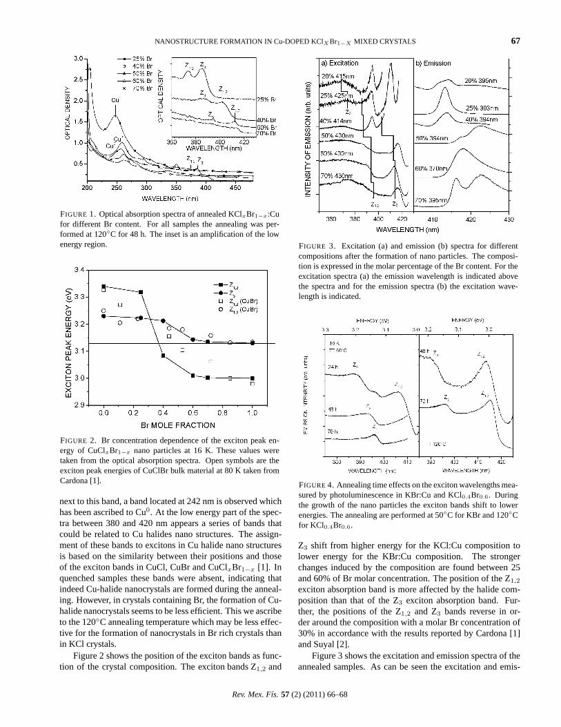
NANOSTRUCTURE FORMATION IN Cu-DOPED KClXBr1−X MIXED CRYSTALS 67
FIGURE 1. Optical absorption spectra of annealed KClxBr1−x:Cufor different Br content. For all samples the annealing was per-formed at 120C for 48 h. The inset is an amplification of the lowenergy region.
FIGURE 2. Br concentration dependence of the exciton peak en-ergy of CuClxBr1−x nano particles at 16 K. These values weretaken from the optical absorption spectra. Open symbols are theexciton peak energies of CuClBr bulk material at 80 K taken fromCardona [1].
next to this band, a band located at 242 nm is observed whichhas been ascribed to Cu0. At the low energy part of the spec-tra between 380 and 420 nm appears a series of bands thatcould be related to Cu halides nano structures. The assign-ment of these bands to excitons in Cu halide nano structuresis based on the similarity between their positions and thoseof the exciton bands in CuCl, CuBr and CuClxBr1−x [1]. Inquenched samples these bands were absent, indicating thatindeed Cu-halide nanocrystals are formed during the anneal-ing. However, in crystals containing Br, the formation of Cu-halide nanocrystals seems to be less efficient. This we ascribeto the 120C annealing temperature which may be less effec-tive for the formation of nanocrystals in Br rich crystals thanin KCl crystals.
Figure 2 shows the position of the exciton bands as func-tion of the crystal composition. The exciton bands Z1,2 and
FIGURE 3. Excitation (a) and emission (b) spectra for differentcompositions after the formation of nano particles. The composi-tion is expressed in the molar percentage of the Br content. For theexcitation spectra (a) the emission wavelength is indicated abovethe spectra and for the emission spectra (b) the excitation wave-length is indicated.
FIGURE4. Annealing time effects on the exciton wavelengths mea-sured by photoluminescence in KBr:Cu and KCl0.4Br0.6. Duringthe growth of the nano particles the exciton bands shift to lowerenergies. The annealing are performed at 50C for KBr and 120Cfor KCl0.4Br0.6.
Z3 shift from higher energy for the KCl:Cu composition tolower energy for the KBr:Cu composition. The strongerchanges induced by the composition are found between 25and 60% of Br molar concentration. The position of the Z1,2
exciton absorption band is more affected by the halide com-position than that of the Z3 exciton absorption band. Fur-ther, the positions of the Z1,2 and Z3 bands reverse in or-der around the composition with a molar Br concentration of30% in accordance with the results reported by Cardona [1]and Suyal [2].
Figure 3 shows the excitation and emission spectra of theannealed samples. As can be seen the excitation and emis-
Rev. Mex. Fıs. 57 (2) (2011) 66–68

68 A. PEREZ-RODRIGUEZ, R. ACEVES, T.M. PITERS, R. RODRIGUEZ-MIJANGOS, AND R. PEREZ-SALAS
sion bands related to Cu halide excitons are located in thesame spectral range. Furthermore the excitation and emis-sion spectra reveal the appearance of additional bands inthe mixed crystals which may be due to the formation ofCu halide nanoparticles with different compositions. Thesefindings hamper the interpretation of the spectra significantlysince the excitation bands related to a specific level can not bemeasured with the emission of that same level due to the in-terference of the intense excitation light with the weak emis-sion of that level. As a consequence the excitation spectrahave to be measured with emission light different than thatof the corresponding levels so that the resulting spectra onlyreflect a distorted view on the behavior of the correspondingexciton bands. Nevertheless some general features observedin the absorption spectra can be recognized in the excitationspectra. Also the shift of the position of the exciton bands tolower energies with increasing size of the nanoparticles dur-ing annealing could be observed in a similar way as has beenobserved for NaCl:Cu [5]. Figure 4 shows this effect for aKBr:Cu and a KCl0.4Br0.6:Cu sample.
The optical absorption and luminescence spectra of theCu+ doped mixed crystals show bands related to nanoparti-cles. The measurements of excitation and emission spectrahowever are hampered by the fact that the wavelength rangeof the exciton emission bands is close to and partly overlap-ping the wavelength range of the exciton excitation bandssuch that the intense excitation light interferes with the weakemission light. The exciton bands in the absorption spectra of
the KClxBr1−x mixed crystals shift from low to high energywith increasing valuex for the composition. The comparisonof this behavior with that of the optical absorption spectra ofCuClxBr1−x mixed crystals, indicate that the nanoparticlesformed in the KClxBr1−x mixed crystals have a similar com-position as the host. This suggest that the migration of Cu+ isprincipally on the cation lattice so that during the formationof nanocrystals the Cu+ substitutes the K+ without modify-ing the Cl−/Br− ratio. On the other hand the additional bandsin the excitation and emission spectra suggest the formationof Cu halide nanoparticles with different compositions indi-cating the migration of halogens on the anion latice.
4. Conclusions
In conclusion we have found that Cu halide nanoparticlescan be formed in KClxBr1−x mixed crystals and that thedominant composition of these nanoparticles is the same asthat of the bulk material. Nanoparticles with other composi-tions seem to be present too but further systematic researchis needed to confirm and clarify the composition of thesenanoparticles.
Acknowledgement
This work has been partially supported by a PROMEP projectP/CA-51 2006-26-18 of the PIFI 2007-26-38-108.
1. M. Cardona,Phys. Rev.129(1963) 69.
2. G. Suyal, M. Menning, and H. Schmidt,J. Mater. Chem.12(2002) 3136.
3. Y. Li, M. Ohta, and A. Nakamura,Phys. Rev. B.57 (1998)R12673.
4. A. Perez-Rodrıguez, M. Flores-Acosta, R. Rodrıguez-Mijangos, and R. Perez-Salas,Rev. Mex. Fıs.52 (2006) 151.
5. M. Haselhoff and H.J. Weber,Phys. Rev. B.58 (1998) 5052.
6. K. Yamanaka, K Edamatsu, and T Itoh,J. Luminescence76&77(1998) 256.
7. K. Yamanaka, K Edamatsu, and T Itoh,J. Luminescence87-89(2000) 312.
Rev. Mex. Fıs. 57 (2) (2011) 66–68

REVISTA MEXICANA DE FISICA S57 (2) 69–74 ABRIL 2011
Photovoltaic conversion of TiO2 nanocrystals decorated with P3OT, Aunanocystal or CdSe quantum dots
I. Zarazuaa, E. De la Rosaa,∗, T. Lopez-Lukea, J. Reyes-Gomezb, S. Ruiza, and R.A. RodriguezcaCentro de Investigaciones enOptica,
Apartado Postal 1-948 Leon, Gto. 37150 Mexico,bFacultad de Ciencias, Universidad de Colima,
Colima, Col. 28045 Mexico,cUniversidad de Guadalajara en Lagos de moreno,
Lagos de Moreno, Jal. 47460 Mexico,∗e-mail: [email protected]
Recibido el 28 de mayo de 2008; aceptado el 4 de junio de 2008
In this work, the preparation and photovoltaic conversion characterization of 10µm films of sensitized TiO2 is reported. The 300 nm TiO2particles with anatase crystalline phase were deposited on an ITO substrate and decorated with Au nanocrystals, P3OT or CdSe QuantumDots (QD’s). The photocurrent was measured in a three electrode electrochemical cell. The results exhibited that QD’s sensitized TiO2 filmshave the largest photocurrent (237µA/cm2), giving a photo-conversion efficiency of 0.149%, more than fourfold the photocurrent of TiO2
without sensitized (0.034%). These results are attributed to the ability of QD’s to photogenerate charge carriers efficiently giving a greatamount of electrons to increase the photocurrent.
Keywords: Solar cells; nanoparticles; TiO2; CdSe; P3OT; Au.
En este trabajo se reporta la preparacion y caracterizacion de pelıculas de 10µm de espesor de TiO2 sensibilizado. Las partıculas de TiO2 de300 nm con fase cristalina anatasa fueron depositadas en un substrato de ITO y decoradas con nanocristales de Au, P3OT o puntos cuanticosde CdSe (QD’s).Despues, se midio fotocorriente en una celda elctroquımica de tres electrodos. Los resultados muestran que las pelıculasde TiO2 sensibilizadas con QD tienen la mayor fotocorriente (237µA), resultando en una eficiencia de fotoconversion de 0.149%, cuatroveces mayor a la eficiencia de las pelıculas de TiO2 sin sensibilizar (0.034%). Estos resultados se atribuyen a la habilidad de los QD’s defotogenerar eficientemente portadores de carga, que contribuiran para incrementar la fotocorriente.
Descriptores: Celdas solares; nano partıculas; TiO2; CdSe; P3OT; Au.
PACS: 88.40.Hj; 88.40.Jr; 78.67.Bf; 78.67.Hc
1. Introduction
In the last years, there has been an increase in the researchof sustainable alternative energy processes. It is a result ofthe reserve decrease of fossil fuels and its environmental ef-fect. Photovoltaic Cells have received significant attentionbecause the solar energy on the earth is1012 times more pow-erful than any other source in the planet. The most commonsolar cells, the silicon solar cells, have a photo-conversion ef-ficiency of 20%, but the manufacturing process is very expen-sive and involves the use of toxic chemicals. The use of nano-structurated materials allow reduce the cost of production dueto the lower synthesis temperatures and deposition methods,although photoconversion efficiency (η) is today lower thanthe best silicon based solar cells. The advantage of nanos-tructurated solar cells is the possibility to manipulate factorslike shape and size of the particles to improveη and makethem commercially feasible. One of the most studied nanos-tructurated solar cells are the Gratzel or dye sensitized solarcells (DSSC) [5]. This kind of cells consist in TiO2 nanopar-ticles acting as a highly porous wide band gap semiconduc-tor electron acceptor layer and a dye adsorbed onto the TiO2
acting as sensitizer to harvest more of the solar flux. Underirradiation, the photo-exited dye molecules inject electrons
into the TiO2 layer and are transported through this layer tobe collected by ITO film on the glass surface. The largestphotoconversion efficiency of DSSC reported in literature is11% [6]. The principal problem in DSSC is, the use of aliquid electrolyte, necessary to reverse the oxidation of dye,that evaporates at room temperature and reduces the life timeof the cell. In addition, the largest conversion efficiency hasbeen obtained with a dye based on Ruthenium that has a greatphotogeneration of charge carriers . However, is very expen-sive and require an increment of the charge carriers injectionto avoid the recombination.
An alternative to DSSC is the use of CdSe Quantum Dots(QD’s) as sensitizer instead of the expensive Ru-complexDyes. QD’s have a large extinction coefficient in the vis-ible absorbing strongly that light and injecting electrons tothe conduction band of metal oxides, contributing to increasethe solar energy conversion. Attachment of QD’s to TiO2
could be done by immersion method using a molecular linker.This kind of solar cells have a photoconversion efficiency of∼3 %, however it presents a Quantum Efficiency (QE) of12% [7,10]. In this kind of cells is necessary to improve theinjection efficiency to increaseη and still having the problemof the liquid electrolyte.
70 I. ZARAZUA, E. DE LA ROSA, T. LOPEZ-LUKE, J. REYES-GOMEZ, S. RUIZ, AND R.A. RODRIGUEZ
Another alternative to DSSC are the solid-state hybridorganic-inorganic solar cells HSC. In these devices, the in-organic component is a metal oxide and a dye is used as lightabsorber like in DSSC. However, in this case, the regenera-tion of the dye is done for a hole injector-polymer. Thiophenederivates seem to be the bests option for this purpose [1].This configuration present less efficiency than the DSSC butpresent as advantage a longer life time due to polymer photo-stability. Cells made of metal oxides usually comprise a mul-tilayer structure with metal oxide in the bottom layer andhole acceptor polymer in the top layer, so, the extent of thedonor acceptor interface depends on the interpenetration ofthe polymer in the metal oxide, that implies the needed fora mesoporous metal oxide. This is the reason for the lowerefficiency of HSC’s and a important topic of research in solarcells [4,9]. It is possible to use a polymer as sensitizer but theefficiency drops [1].
Semiconductor-metal nanocomposites have been widelystudied in photocatalysis. The metal in contact with the semi-conductor enhances the efficiency improving the charge sepa-ration process, the photocurrent and photovoltage [15]. Stud-ies have shown a shift in the fermi level to more negativelevel by doping semiconductor with a metal ion. That shiftenhances the efficiency of interfacial charge transfer pro-cess [2]. Gold nanoparticles have the ability to undergo qua-tized charging, that make them the best candidate to achieveFermi-Level equilibration [3]. Gold have a size dependenceconductance increasing by decreasing the size [15].
Nanostructured TiO2 have many features that can af-fect the photoconversion efficiency. Size affects the elec-tron transport, by increasing the particle size defects andgrain boundaries are reduced, consequently the charge carri-ers recombination decrease resulting in a fill factor gain [14].In addition, the sensitizer metal-oxide interaction area is re-duced that is expressed as photocurrent decrease. TiO2 ex-ists in three crystalline phase, anatase, rutile, and brookite;each phase presents different electrical proprieties. Anataseand rutile have been used for photovoltaic cells, meanwhilebrookite has no received similar attention because it is themost difficult to prepare as a thin film. A better crystallinityimplies less defects and less recombination sites. The par-ticle shape is an important factor in the efficiency of solarcells, some shapes foment a preferential flux of electrons“like nanorods” [16], and others give a major interactionarea between polymer and metal oxide like nanotubes andmesopours spheres. Particle connectivity plays an importantrole, a major connectivity gives better electron conductionbut reduces polymer adsorption [1]. A major efficiency isachieved with a dual layer configuration, a compact layer inthe bottom to obtain good contact with ITO, followed by amesoscopic layer to obtain a good penetration of polymer [1].
Although these kinds of cells had been widely studied,there still unclear the optimal conditions to maximize its ad-vantages, moreover there is no a systematic study to comparethem in similar conditions. In this work, TiO2 films weresynthesized by sol-gel method, then were decorated with
Au, P3OT or CdSe QD’s to compare the sensitizer photo-conversion efficiency effect via electrochemical characteriza-tion.
2. Experimental
Preparation of TiO2 sensitized films
TiO2 film preparation.TiO2 particles were made by sol-gelmethod. 3.75 mL of titanium isoprpoxide (IV) and PluronicF127 were added in a solution of 5 mL of H2NO3 in 50 mLof EtOH adding 2.5 mL of H2O, the mixture was stirred onehour. The synthesis process was done in a glove box with N2
atmosphere. The mixed solution was transferred into a teflonautoclave. The hydrothermal treatment was carried out at70C during 12 h outside the glove box. The resulting xero-gel was washed three times with EtOH and annealed for onehour at 550C. The TiO2 powder was suspended in C2H5OHand deposited on ITO substrate by doctor blade method.
CdSe QD’s Synthesis.High-quality CdSe QD’s weresynthesized. CdO is used as the Cd precursor and 1-Tetradecylphosphonic acid (TDPA, 99%) and trioctylphos-phine oxide (TOPO, 99%) are the ligands and coordinatingsolvents, respectively. The resulting CdSe nanocrystals werein the strong confinement size regime and were synthesizedin normal air-free reaction conditions. The synthesis of theCdSe nanoparticle follows the procedure reported by Robelet al., wherein 0.05 g ( 0.39 mmol) of CdO, 0.3 g (1.1mmol)of TDPA, and 4 g of TOPO were heated to 110C and de-gassed under vacuum and then heated to 300C under a ni-trogen flow [13]. A SeTOP (0.7% by weight) solution wasobtained by adding 0.026 g of Se powder with 4.25 mL ofTOP inside of a glove box and stirring for 1 h to ensure com-plete dissolution of the Se powder. After reaching 300C, theCd-TDPA-TOPO solution was cooled to 270C prior to theinjection of SeTOP. Under a nitrogen flow, 3 mL of SeTOPwas injected, which resulted in the lowering of the tempera-ture to 260C. The temperature was then increased to 280Cto facilitate particle growth, and aliquots were removed andprobed to track nanocrystallite growth via UV-vis absorptionspectroscopy. The CdSe solution was cooled and removedfrom the reaction flask at around 80C and dissolved into10 mL of toluene. The QD’s in toluene were then cleanedtwice through a precipitation and decantation regime usingmethanol and centrifugation at 3000 rpm, and the QD’s wereultimately redissolved in toluene prior to their use as a sensi-tizer.
Au Nanocrystals Synthesis.Au nanocrystals were synthe-sized mixing a 0.2 M dissolution of Cetyl trimethylammo-nium bromide (CTAB) with 5 mL of 0.0005 M dissolutionof HAuCl4. The mixture was stirred in ice bath and added0.60 mL of 0.01M NaBH4, as result a brown solution wasobtained. The solution was stirred for 2 h to obtain a 4 nmparticles. The size was proved via UV-vis absorption spec-troscopy. Solution was stored avoiding light exposition untiluse as sensitizer.
Rev. Mex. Fıs. 57 (2) (2011) 69–74

PHOTOVOLTAIC CONVERSION OF TiO2 NANOCRYSTALS DECORATED WITH P3OT, Au NANOCYSTAL OR CdSe QUANTUM DOTS 71
FIGURE 1. Schematic representation of decoration of TiO2 films.a) Functionalization with TGA (R=CH2CO). b) Decoration whitAu.
P3OT Preparation.In this work, poly(3-octylthiophene)supplied by Sigma was used. A solution of 10−5M in tolueneof P3OT was made. The band gap of the P3OT was measuredvia UV-vis absorption spectroscopy derivate. The solutionwas store in dark before its use as sensitizer.
Sensitizers linkage to TiO2. Sensitizers (Au, CdSe QD’sand P3OT) were linked to nanocrystalline TiO2 thin filmsusing TGA (HSCH2COOH) as a molecular linker. TiO2has a strong affinity for the carboxylate group of the linkermolecules (Fig. 1a), while the sulfur atom of TGA bindsstrongly to sensitizers through surface of these (Fig. 1b). Thefilms were dried on a hot plate at 100C for 1 h to removeH2O from the surface due to ambient humidity adsorption.The films were later immersed in TGA diluted at 70% inCH3Cl for 12 h in a nitrogen environment in a glove box.The films were then immersed in toluene removing the ex-cess TGA, and then immersed in a CdSe, P3OT or Au solu-tion for 12 h inside the glove box. Four films of 3.2 cm2 wereimmersed in 6 mL of sensitizers solution. The TiO2 sensi-tized films were stored in a nitrogen-filled glove box and notexposed to light prior to Photoelectrochemistry (PEC) char-acterization. The TiO2 functionalized cell in the electrolyteis very stable; however, when it is removed from the Na2Selectrolyte and are in ambient conditions, the thin film’s prop-erties deteriorate after experimentation. Long-term stabilityneeds to be further studied in future research.
Characterization
Raman Spectroscopy.The raman shift was measured exitingthe TiO2 powder with a HeNe Laser with 60 mW at 680 nmfocusing the beam with a 40X microscope objective. Thespectrum was measured from 200 to 1000 cm−1. Morpho-logical characterization.The shape and size of the TiO2 par-ticles was measured with a JSM-6390 series, JEOL ScanningElectron Microscope.Optical Absorption.The spectra weremeasured with a Perkin Elmer absorption spectrophotometer.
FIGURE 2. SEM image of TiO2 particles.
FIGURE 3. Raman spectrum of TiO2 aged at 70C for 12 hoursand annealed at 550C for an hour, showing characteristic anatasecrystalline phase peaks.
The TiO2 spectra were measured via reflectance in tabletsof compacted powder, scanning between 200 to 800 nm.Using the maxima of the first derivate of the spectra thethreshold of the band gap was estimated.ElectrochemicalCharacterization.The photocurrent was measured in a threeelectrode cell using the sample as work electrode, StaturedCalomel Electrode (SCE) as reference, Pt wire as counter-electrode and Na2S as electrolyte using a potensiostat GamryReference 600. The work electrode was illuminated with31.83 mW/cm2 from a halogen lamp. Na2S provide us NaS−
and SO2−4 as redox couple with standard potential
E0NaS−SO
2−4
= −0.618
volts vs NHE [12].
3. Results and discussion
Structural and morphology characterization
Morphology.The morphology of the TiO2 powder was stud-ied by SEM. The average TiO2 particle size was found to bearound 300 nm in diameter see Fig. 2. This particles have a
Rev. Mex. Fıs. 57 (2) (2011) 69–74

72 I. ZARAZUA, E. DE LA ROSA, T. LOPEZ-LUKE, J. REYES-GOMEZ, S. RUIZ, AND R.A. RODRIGUEZ
FIGURE 4. Absorption spectra and its derivate of, a)TiO2 , b)P3OTand QD’s and c)Au. Doted lines represent the first derivate.
quasi spheric shape and are composed for an agglomerate ofmany nanocrystals.
Raman Spectroscopy.Figure 3 shows raman spectrumfor the TiO2 powder. Raman spectrum has the well definedcharacteristic peaks of anatase crystalline phase of TiO2 [17]indicating a high crystallinity. It can be seen that the charac-teristic peak for the anatase phase are centered at 395 cm−1,513 cm−1 and 635 cm−1.
Optical Absorption
The absorption spectra of TiO2, P3OT, QD’s and Au areshown in solid lines in Fig. 4. The representative absorp-tion peaks for TiO2, P3OT and QD’s are centered at 3.69,2.7, and 2.82 eV respectively. The first derivate of the ab-sorption spectra evidence peaks centered at 3.34, 2.75 and2.47 eV associated to the band gap of TiO2, QD’s and P3OT,
FIGURE 5. I-V characteristic of decorated and no decorated TiO2.
TABLE I. Efficiency of the solar cells under 31.83 mW/cm2 halo-gen lamp illumination
Sample Jsc Voc FF η
µA mV % %
TiO2-QD’s 237 447 44.4 0.149
TiO2-Au 183 437 51.8 0.130
TiO2-P3OT 124 443 46.6 0.080
TiO2 102 594 18.1 0.034
respectively, as is shown in Figs. 4a, 4b. The band gap ofP3OT and QD’s are lower than the one of TiO2. These ma-terials spectra shows an obvious red shift of the absorptionedge toward the visible region, allowing increase the photo-conversion efficiency. P3OT have a wider absorption peakthan QD’s. The Au nanoparticles present an absorption peakat 544 nm see Fig. 4c, corresponding to the plasmon reso-nance associated to the nanoparticle size (4 nm) [8].
Electrochemical Characterization:
The current-voltage (I-V) profiles for solar cells fabricatedwith different sensitizers were obtained. In Fig. 5 can beappreciated that all decorated systems have a higher pho-tocurrent than TiO2 films without sensitizers. The highestphotocurrent was achieved for the TiO2-QD’s and the lowerone for TiO2-P3OT cell. The short-circuit current and open-circuit voltage found in Fig. 5 are summarized in Table I.The Fill Factor (FF) and power conversion efficiency (η) arealso listed in Table I and were calcualted by using the equa-tions [11]
FF =Pmax
Jsc ∗ Voc, (1)
η =Pmax
Pl= FF
Jsc ∗ Voc
Pl, (2)
whereJsc is the short-circuit current density, Voc is the open-circuit voltage, Pmax is the maximum power density ob-served from the current density-voltage curve for each device,and Pl is the incident light power density (31.83 mW/cm2).It is clear than TiO2-Au films exhibit the highest FF (51.8%)
Rev. Mex. Fıs. 57 (2) (2011) 69–74
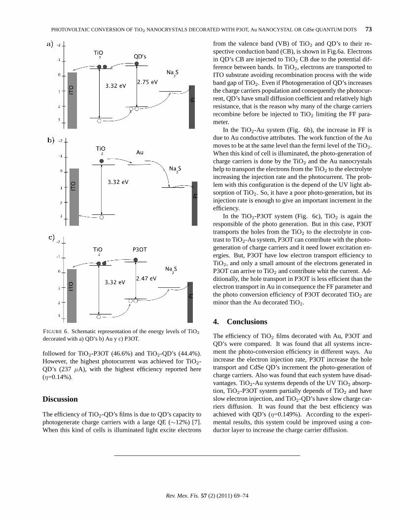
PHOTOVOLTAIC CONVERSION OF TiO2 NANOCRYSTALS DECORATED WITH P3OT, Au NANOCYSTAL OR CdSe QUANTUM DOTS 73
FIGURE 6. Schematic representation of the energy levels of TiO2
decorated with a) QD’s b) Au y c) P3OT.
followed for TiO2-P3OT (46.6%) and TiO2-QD’s (44.4%).However, the highest photocurrent was achieved for TiO2-QD’s (237 µA), with the highest efficiency reported here(η=0.14%).
Discussion
The efficiency of TiO2-QD’s films is due to QD’s capacity tophotogenerate charge carriers with a large QE (∼12%) [7].When this kind of cells is illuminated light excite electrons
from the valence band (VB) of TiO2 and QD’s to their re-spective conduction band (CB), is shown in Fig.6a. Electronsin QD’s CB are injected to TiO2 CB due to the potential dif-ference between bands. In TiO2, electrons are transported toITO substrate avoiding recombination process with the wideband gap of TiO2. Even if Photogeneration of QD’s increasesthe charge carriers population and consequently the photocur-rent, QD’s have small diffusion coefficient and relatively highresistance, that is the reason why many of the charge carriersrecombine before be injected to TiO2 limiting the FF para-meter.
In the TiO2-Au system (Fig. 6b), the increase in FF isdue to Au conductive attributes. The work function of the Aumoves to be at the same level than the fermi level of the TiO2.When this kind of cell is illuminated, the photo-generation ofcharge carriers is done by the TiO2 and the Au nanocrystalshelp to transport the electrons from the TiO2 to the electrolyteincreasing the injection rate and the photocurrent. The prob-lem with this configuration is the depend of the UV light ab-sorption of TiO2. So, it have a poor photo-generation, but itsinjection rate is enough to give an important increment in theefficiency.
In the TiO2-P3OT system (Fig. 6c), TiO2 is again theresponsible of the photo generation. But in this case, P3OTtransports the holes from the TiO2 to the electrolyte in con-trast to TiO2-Au system, P3OT can contribute with the photo-generation of charge carriers and it need lower excitation en-ergies. But, P3OT have low electron transport efficiency toTiO2, and only a small amount of the electrons generated inP3OT can arrive to TiO2 and contribute whit the current. Ad-ditionally, the hole transport in P3OT is less efficient than theelectron transport in Au in consequence the FF parameter andthe photo conversion efficiency of P3OT decorated TiO2 areminor than the Au decorated TiO2.
4. Conclusions
The efficiency of TiO2 films decorated with Au, P3OT andQD’s were compared. It was found that all systems incre-ment the photo-conversion efficiency in different ways. Auincrease the electron injection rate, P3OT increase the holetransport and CdSe QD’s increment the photo-generation ofcharge carriers. Also was found that each system have disad-vantages. TiO2-Au systems depends of the UV TiO2 absorp-tion, TiO2-P3OT system partially depends of TiO2 and haveslow electron injection, and TiO2-QD’s have slow charge car-riers diffusion. It was found that the best efficiency wasachieved with QD’s (η=0.149%). According to the experi-mental results, this system could be improved using a con-ductor layer to increase the charge carrier diffusion.
Rev. Mex. Fıs. 57 (2) (2011) 69–74

74 I. ZARAZUA, E. DE LA ROSA, T. LOPEZ-LUKE, J. REYES-GOMEZ, S. RUIZ, AND R.A. RODRIGUEZ
1. M. Antoniadou, E. Stathatos, N. Boukos, and A. Stefopoulos,Nanotechnology20 (2009) 495201.
2. G. Burgeth and H. Kisch,Chem. Rev230(2002) 40.
3. Shaowei Chen and R.W. Murray,J. Phys. Chem. B103 (1999)9996.
4. C. Goh, S.R. Scully, and M.D. McGehee,J. Appl. Phys.101(2007) 114503.
5. C.D. Grantet al., Synth. Met132(2003) 197.
6. M. Green, K. Emery, Y. Hishikawa, and W. Warta,Prog. Pho-tovolt: Res. Appl.17 (2009) 85.
7. N. Greenham, X. Peng, and A. Alivisatos,Phys. Rev. B54(1996) 17628.
8. N.R. Jana, L. Gearheart, and C.J. Murphy,J. Phys. Chem. B105(2001) 4065.
9. Y.Y. Lin, T.H. Chu, C.W. Chen, and W.F. Su,Appl. Phys. Lett.92 (2008) 053312.
10. T. Lopez-Lukeet al., J. Phys. Chem. C112(2008) 1282.
11. B. O’Regan and M. Gratzel,Nature353(1991) 353.
12. M. Pourbaix,Atlas of Electrochemecal Equilibria in AqueusSolutions(National Association of Corrosion Engineers, sec-ond ed., 1974) pp. 97.
13. I. Robel, V. Subramanian, M. Kuno, and P.V. Kamat,J. Am.Chem. Soc.128(2006) 2385.
14. Tetsuo Soga,Nanostructured Materials for Solar Energy Con-version, (Elsevier, Radarweg 29, PO Box 211, 1000 AE Am-sterdam, The Netherlands The Boulevard, Langford Lane,Kidlington, Oxford OX5 1GB, UK, 2006).
15. V. Subramanian, E.E. Wolf, and P.V Kamat,J. Am. Chem. Soc.126(2003) 4943.
16. A. Wolcott, W.A. Smith, T.R. Kuykendall, Y. Zhao, and J.Z.Zhang,Pho- toelectrochemical water splitting using dense andaligned TiO2 nanorod arrays, Small5 (2009) 104.
17. Jian zhu Yuning Huo, Yi jina and Hexing li,Appl. Catalysis B89 (2008) 543.
Rev. Mex. Fıs. 57 (2) (2011) 69–74

REVISTAMEXICANA DE
FISICAS
VOLUMEN 57NUMERO 2
ABRIL2011
CONTENIDO/CONTENTSCatalytic activity of MoS2 nanotubes in the hydrodesulphurization reactionof dibenzothiophene,
F.L. DEEPAK, R.P. HERNANDEZ, J. CRUZ-REYES, S. FUENTES,AND M.J. YACAMAN 1–6
Structural and optical characterization of InxGa1−xN nano-structured grownby chemical vapor deposition,
A. RAMOS-CARRAZCO, E. CHAIKINA , O.E. CONTRERAS, M. BARBOZA-FLORES
AND R. GARCIA 7–9Synthesis and characterization of In-doped ZnO nano-powders produced bycombustion synthesis,
R. GARCIA , R. NUNEZ-GONZALEZ, D. BERMAN-MENDOZA, M. BARBOZA-FLORES
AND R. RANGEL 10–12Photoconductivity studies of gold nanoparticles supported on amorphous andcrystalline TiO2 matrix prepared by sol-gel method,
G. VALVERDE-AGUILAR , J.A. GARCIA -MACEDO, V. RENTERIA-TAPIA ,AND M. AGUILAR-FRANCO 13–18
Integration and electrical characterization of organic thin film transistor for anactive matrix of oleds,
G. GUTIERREZ-HEREDIA, L.A. GONZALEZ , A. AVENDANO, D. BERMAN,H.N. ALSHAREEF, B.E. GNADE, AND M. QUEVEDO-L OPEZ 19–21
Theoretical study of the electronic band gap in β-SiC nanowires,A. TREJO, M. CALVINO , A. E. RAMOS, E. CARVAJAL , AND M. CRUZ-IRISSON 22–25
Dose dependent shift of the TL glow peak in a silicon rich oxide (SRO) film,T.M. PITERS, M. ACEVES-M IJARES, D. BERMAN-MENDOZA,L.R. BERRIEL-VALDOS, AND J.A. LUNA-L OPEZ 26–29
Estudio del desempeno de un catalizador Au/TiO2/SiO2 en la reaccion deoxidacion de CO,
J.A. GARCIA -MACEDO, R. ARREOLA-SANCHEZ, M.A. RIOS-ENRIQUEZ,V.M. RENTERIA -TAPIA Y G. VALVERDE-AGUILAR 30–35
continuacion/continued

continuacion/continued
contenido/contents Rev. Mex. Fıs. S57 (2) (2011) abril 2011
Photocatalytic activity in the visible region of high energy milled TiO2:Nnanopowders,
L. ROJAS-BLANCO, F.J. ESPINOZA-BELTRAN , P.G. MANI -GONZALEZ ,R. RAM IREZ-BON, G. ZAMBRANO , AND J. VELASQUEZ-SALAZAR 36–40
Preparacion de nanoparticulas polimericas con aplicacion farmaceutica usandotecnicas basadas en emulsificacion,
N. NARANJOS-RAM IREZ, D.I. TORRES-CANTU, V.I. CASTILLO-RODRIGUEZ,S.A. GALINDO -RODRIGUEZ, A. CHAVEZ-MONTES, R. CASTRO-RIOS,R. ALVAREZ-ROMAN Y M.E. MARTINEZ-BARBOSA 41–43
Push-pull chromophores aggregation in SiO2 sol-gel films doped with silvernanoparticles,
A. FRANCO, G. BRUSATIN, M GUGLIELMI , V. RENTERIA, G. VALVERDE-AGUILAR ,AND J.A. GARCIA -MACEDO 44–50
Preparation of chitosan/magnetite polymeric-magnetic films,M.A. GARZA-NAVARRO, V. GONZALEZ , M. HINOJOSA, AND A. TORRES-CASTRO 51–56
Synthesis of Gd2O3:Eu3+ nanocrystallites emmbeded in SiO2 usingpolyvinylpyrrolidone (pvp) by sol-gel process,
A. GARCA MURILLO , F. CARRILLO ROMO, M. GARCIA HERNANDEZ,J.C. BADILLO , E. DE LA ROSA, AND T. LOPEZ-LUKE 57–60
Adsorption of gold nanoparticles on silicon substrate and their application inSurface Enhancement Raman Scattering,
F. CASTILLO , E. PEREZ, AND E. DE LA ROSA 61–65Nanostructure formation in Cu-doped KClxBr1−x mixed crystals,
A. PEREZ-RODRIGUEZ, R. ACEVES, T.M. PITERS, R. RODRIGUEZ-M IJANGOS,AND R. PEREZ-SALAS 66–68
Photovoltaic conversion of TiO2 nanocrystals decorated with P3OT, Au nanocystalor CdSe quantum dots,
I. ZARAZUA , E. DE LA ROSA, T. LOPEZ-LUKE, J. REYES-GOMEZ, S. RUIZ ,AND R.A. RODRIGUEZ 69–74