p s fpga u b d - university of california, berkeleyjohnw/papers/protected/...the sobel edge...
TRANSCRIPT
C H A P T E R 8
PROGRAMMING STREAMING FPGAAPPLICATIONS USING BLOCK DIAGRAMSIN SIMULINK
Brian C. RichardsChen ChangJohn WawrzynekRobert W. BrodersenUniversity of California–Berkeley
Although a system designer can use hardware description languages, such asVHDL (Chapter 6) and Verilog to program FPGAs, the algorithm developertypically uses higher-level descriptions to refine an algorithm. As a result, analgorithm described in a language such as Matlab or C is frequently reenteredby hand by the system designer, after which the two descriptions must be verifiedand refined manually. This can be time consuming.
To avoid reentering a design when translating from a high-level simulationlanguage to HDL, the algorithm developer can describe a system from thebeginning using block diagrams in Matlab Simulink [1]. Other block diagramenvironments can be used in a similar way, but the tight integration of Simulinkwith the widely used Matlab simulation environment allows developers to usefamiliar data analysis tools to study the resulting designs. With Simulink, a sin-gle design description can be prepared by the algorithm developer and refinedjointly with the system architect using a common design environment.
The single design entry is enabled by a library of Simulink operator primitivesthat have a direct mapping to HDL, using matching Simulink and HDL modelsthat are cycle accurate and bit accurate between both domains. Examples andcompilation environments include System Generator from Xilinx [2], SynplifyDSP from Synplicity [3], and the HDL Coder from The Mathworks [1]. Usingsuch a library, nearly any synchronous multirate system can be described, withhigh confidence that the result can be mapped to an FPGA given adequateresources.
In this chapter, a high-performance image-processing system is describedusing Simulink and mapped to an FPGA-based platform using a design flow builtaround the Xilinx System Generator tools. The system implements edge detec-tion in real time on a digitized video stream and produces a corresponding videostream labeling the edges. The edges can then be viewed on a high-resolutionmonitor. This design demonstrates how to describe a high-performance parallel

184 Chapter 8 � Programming Streaming FPGA Applications
datapath, implement control subsystems, and interface to external devices,including embedded processors.
8.1 DESIGNING HIGH-PERFORMANCE DATAPATHS USING STREAM-BASEDOPERATORSWithin Simulink we employ a Synchronous Dataflow computational model(SDF), described in the Synchronous Dataflow, Section 5.1.3, of Chapter 5. Eachoperator is executed once per clock cycle, consuming input values and producingnew output values once per clock tick. This discipline is well suited for stream-based design, encouraging both the algorithm designer and the system architectto describe efficient datapaths with minimal idle operations.
Clock signals and corresponding clock enable signals do not appear in theSimulink block diagrams using the System Generator libraries, but are automati-cally generated when an FPGA design is compiled. To support multirate systems,the System Generator library includes up-sample and down-sample blocks tomark the boundaries of different clock domains. When compiled to an FPGA,clock enable signals for each clock domain are automatically generated.
All System Generator components offer compile time parameters, allowingthe designer to control data types and refine the behavior of the block. Hier-archical blocks, or subsystems in Simulink, can also have user-defined parame-ters, called mask parameters. These can be included in block property expres-sions within that subsystem to provide a means of generating a variety ofbehaviors from a single Simulink description. Typical mask parameters includedata type and precision specification and block latency to control pipelinestage insertion. For more advanced library development efforts, the maskparameters can be used by a Matlab program to create a custom schematic atcompile time.
The System Generator library supports fixed-point or Boolean data types formapping to FPGAs. Fixed-point data types include signed and unsigned values,with bit width and decimal point location as parameters. In most cases, theoutput data types are inferred automatically at compile time, although manyblocks offer parameters to define them explicitly.
Pipeline operators are explicitly placed into a design either by inserting delayblocks or by defining a delay parameter in selected functional blocks. Althoughthe designer is responsible for balancing pipeline operators, libraries of high-level components have been developed and reused to hide pipeline-balancingdetails from the algorithm developer.
The Simulink approach allows us to describe highly concurrent SDF systemswhere many operators—perhaps the entire dataflow path—can operate simulta-neously. With modern FPGAs, it is possible to implement these systems withthousands of simultaneous operators running at the system clock rate withlittle or no control logic, allowing complex, high performance algorithms to beimplemented.

8.2 An Image-processing Design Driver 185
8.2 AN IMAGE-PROCESSING DESIGN DRIVER
The goal of the edge detection design driver is to generate a binary bit mask froma video source operating at up to a 200 MHz pixel rate, identifying where likelyedges are in an image. The raw color video is read from a neighboring FPGAover a parallel link, and the image intensity is then calculated, after which two3×3 convolutional Sobel operator filters identify horizontal and vertical edges;the sum of their absolute values indicates the relative strength of a feature edgein an image. A runtime programmable gain (variable multiplier) followed by anadjustable threshold maps the resulting pixel stream to binary levels to indicateif a given pixel is labeled as an edge of a visible feature. The resulting videomask is then optionally mixed with the original color image and displayed ona monitor.
Before designing the datapaths in the edge detection system, the data andcontrol specification for the video stream sources and sinks must be defined.By convention, stream-based architectures are implemented by pairing datasamples with corresponding control tags and maintaining this pairing throughthe architecture. For this example, the video data streams may have varying datatypes as the signals are processed whereas the control tags are synchronizationsignals that track the pipeline delays in the video stream. The input video streamand output display stream represent color pixel data using 16 bits—5 bits forred, 6 bits for green, and 5 bits for blue unsigned pixel intensity values. Inter-mediate values might represent video data as 8-bit grayscale intensity values oras 1-bit threshold detection mask values.
As the data streams flow through the signal-processing datapath, the oper-ators execute at a constant 100 MHz sample rate, with varying pipeline delaysthrough the system. The data, however, may arrive at less than 100 MHz, requir-ing a corresponding enable signal (see the discussion of data presence sub-section in Chapter 5, Section 5.2.1) to tag valid data. Additionally, hysync,vsync, and msync signals are defined to be true for the first pixel of each row,frame, and movie sequence, respectively, allowing a large variety of video streamformats to be supported by the same design.
Once a streaming format has been specified, library components can bedeveloped that forward a video stream through a variety of operators to createhigher-level functions while maintaining valid, pipeline-delayed synchronizationsignals. For blocks with a pipeline latency that is determined by mask param-eters, the synchronization signals must also be delayed based on the maskparameters so that the resulting synchronization signals match the processeddata stream.
8.2.1 Converting RGB Video to GrayscaleThe first step in this example is to generate a grayscale video stream from theRGB input data. The data is converted to intensity using the NTSC RGB-to-Ymatrix:
Y = 0.3 ∗ red +0.59 ∗ green +0.11 ∗ blue

186 Chapter 8 � Programming Streaming FPGA Applications
FIGURE 8.1 � An RGB-to-Y (intensity) Simulink diagram.
This formula is implemented explicitly as a block diagram, shown in Figure 8.1,using constant gain blocks followed by adders. The constant multiplicationvalues are defined as floating-point values and are converted to fixed-pointaccording to mask parameters in the gain model. This allows the precision ofthe multiplication to be defined separately from the gain, leaving the synthesistools to choose an implementation. The scaled results are then summed with anexplicit adder tree.
Note that if the first adder introduces a latency of adder_delay clock cycles,the b input to the second adder, add2, must also be delayed by adder_delaycycles to maintain the cycle alignment of the RGB data. Both the Delay1 blockand the add1 block have a subsystem mask parameter defining the delay thatthe block will introduce, provided by the mask parameter dialogue as shown inFigure 8.2. Similarly, the synchronization signals must be delayed by three cyclescorresponding to one cycle for the gain blocks, one cycle for the first adder,

8.2 An Image-processing Design Driver 187
FIGURE 8.2 � A dialogue describing mask parameters for the rgb—to—y block.
and one cycle for the second adder. By designing subsystems with configurabledelays and data precision parameters, library components can be developed toencourage reuse of design elements.
8.2.2 Two-dimensional Video FilteringThe next major block following the RGB-to-grayscale conversion is the edgedetection filter itself (Figure 8.3), consisting of two pixel row delay lines, two3×3 kernels, and a simplified magnitude detector. The delay lines store the tworows of pixels preceding the current row of video data, providing three streamsof vertically aligned pixels that are connected to the two 3×3 filters—the firstone detecting horizontal edges and the second detecting vertical edges. Thesefilters produce two signed fixed-point streams of pixel values, approximatingthe edge gradients in the source video image.
On every clock cycle, two 3 × 3 convolution kernels must be calculated,requiring several parallel operators. The operators implement the followingconvolution kernels:
−1 0 +1 +1 +2 +1Sobel X Gradient: −2 0 +2 Sobel Y Gradient: 0 0 0
−1 0 +1 −1 −2 −1

188 Chapter 8 � Programming Streaming FPGA Applications
FIGURE 8.3 � The Sobel edge detection filter, processing an 8-bit video datastream to produce a stream ofBoolean values indicating edges in the image.
To support arbitrary kernels, the designer can choose to implement the Sobeloperators using constant multiplier or gain blocks followed by a tree of adders.For this example, the subcircuits for the x- and y-gradient operators are hand-optimized so that the nonzero multipliers for both convolution kernels areimplemented with a single hardwired shift operation using a power-of-2 scaleblock. The results are then summed explicitly, using a tree of add or subtractoperators, as shown in Figures 8.4 and 8.5.
Note that the interconnect in Figures 8.4 and 8.5 is shown with the data typesdisplayed. For the most part, these are assigned automatically, with the inputdata types propagated and the output data types and bit widths inferred to avoidoverflow or underflow of signed and unsigned data types. The bit widths can becoerced to different data types and widths using casting or reinterpret blocks,and by selecting saturation, truncation, and wraparound options available toseveral of the operator blocks. The designer must exercise care to verify thatsuch adjustments to a design do not change the behavior of the algorithm.
Through these Simulink features a high-level algorithm designer can directlyexplore the impact of such data type manipulation on a particular algorithm.
Once the horizontal and vertical intensity gradients are calculated for theneighborhood around a given pixel, the likelihood that the pixel is near theboundary of a feature can be calculated. To label a pixel as a likely edge ofa feature in the image, the magnitude of the gradients is approximated and theresulting nonnegative value is scaled and compared to a given threshold. The

8.2 An Image-processing Design Driver 189
FIGURE 8.4 � The sobel—y block for estimating the horizontal gradient in the source image.
FIGURE 8.5 � The sobel—x block for estimating the vertical gradient in the source image.
190 Chapter 8 � Programming Streaming FPGA Applications
magnitude is approximated by summing the absolute values of the horizontaland vertical edge gradients, which, although simpler than the exact magnitudecalculation, gives a result adequate for our applications.
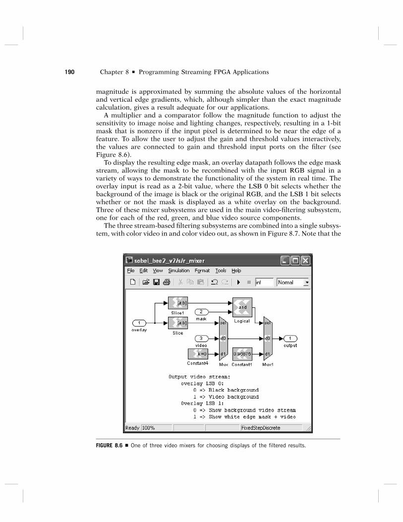
A multiplier and a comparator follow the magnitude function to adjust thesensitivity to image noise and lighting changes, respectively, resulting in a 1-bitmask that is nonzero if the input pixel is determined to be near the edge of afeature. To allow the user to adjust the gain and threshold values interactively,the values are connected to gain and threshold input ports on the filter (seeFigure 8.6).
To display the resulting edge mask, an overlay datapath follows the edge maskstream, allowing the mask to be recombined with the input RGB signal in avariety of ways to demonstrate the functionality of the system in real time. Theoverlay input is read as a 2-bit value, where the LSB 0 bit selects whether thebackground of the image is black or the original RGB, and the LSB 1 bit selectswhether or not the mask is displayed as a white overlay on the background.Three of these mixer subsystems are used in the main video-filtering subsystem,one for each of the red, green, and blue video source components.
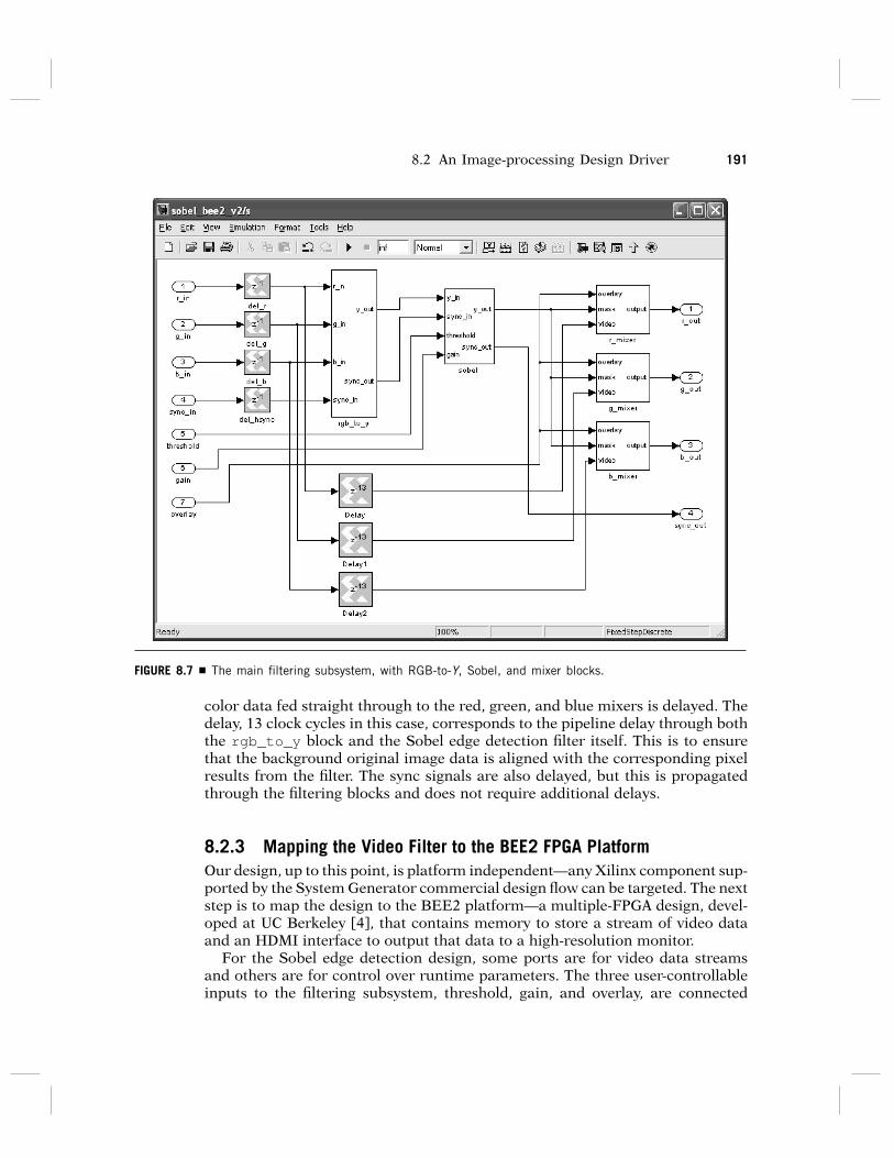
The three stream-based filtering subsystems are combined into a single subsys-tem, with color video in and color video out, as shown in Figure 8.7. Note that the
FIGURE 8.6 � One of three video mixers for choosing displays of the filtered results.
8.2 An Image-processing Design Driver 191
FIGURE 8.7 � The main filtering subsystem, with RGB-to-Y, Sobel, and mixer blocks.
color data fed straight through to the red, green, and blue mixers is delayed. Thedelay, 13 clock cycles in this case, corresponds to the pipeline delay through boththe rgb_to_y block and the Sobel edge detection filter itself. This is to ensurethat the background original image data is aligned with the corresponding pixelresults from the filter. The sync signals are also delayed, but this is propagatedthrough the filtering blocks and does not require additional delays.
8.2.3 Mapping the Video Filter to the BEE2 FPGA PlatformOur design, up to this point, is platform independent—any Xilinx component sup-ported by the System Generator commercial design flow can be targeted. The nextstep is to map the design to the BEE2 platform—a multiple-FPGA design, devel-oped at UC Berkeley [4], that contains memory to store a stream of video dataand an HDMI interface to output that data to a high-resolution monitor.
For the Sobel edge detection design, some ports are for video data streamsand others are for control over runtime parameters. The three user-controllableinputs to the filtering subsystem, threshold, gain, and overlay, are connected

192 Chapter 8 � Programming Streaming FPGA Applications
to external input ports, for connection to the top-level testbench. The filter,included as a subsystem of this testbench design, is shown in Figures 8.8 and 8.9.So far, the library primitives used in the filter are independent of both the typeof FPGA that will be used and the target testing platform containing the FPGA.
To support targeting the filter to the BEE2 FPGA platform for real-time test-ing, a set of libraries and utilities from the BEE Platform Studio, also developedat Berkeley, is used [5]. Several types of library blocks are available to assist withplatform mapping, including simple I/O, high-performance I/O, and micropro-cessor register and memory interfaces.
The strategy for using the Simulink blocks to map a design to an FPGAassumes that a clear boundary is defined to determine which operatorsare mapped to the FPGA hardware and which are for simulation only. Thecommercial tools and design flows for generating FPGA bit files assume thatthere are input and output library blocks that appear to Simulink as, respec-tively, double-precision to fixed-point conversion and fixed-point to double typeconversion blocks. For simulation purposes, these blocks allow the hardware
FIGURE 8.8 � The top-level video testbench, with input, microprocessor register, and configuration blocks.

8.2 An Image-processing Design Driver 193
FIGURE 8.9 � The output section of the top-level testbench, with a 10G XAUI interface block.
description to be simulated with a software testbench to verify basic function-ality before mapping the design to hardware. They also allow the designer toassign the FPGA pin locations for the final configuration files.
The BEE Platform Studio (BPS) [5] provides additional I/O blocks that allowthe designer to select pin locations symbolically, choosing pins that are hardwiredto other FPGAs, LEDs, and external connections on the platform. The designeris only required to select a platform by setting BPS block parameters, and doesnot need to keep track of I/O pin locations. This feature allows the designer toexperiment with architectural tradeoffs without becoming a hardware expert.
In addition to the basic I/O abstractions, the BPS allows high-performance oranalogue I/O devices to be designed into a system using high-level abstractions.For the video-testing example, a 10 Gbit XAUI I/O block is used to output thecolor video stream to platform-specific external interfaces. The designer selectsthe port to be used on the actual platform from a pulldown menu of availablenames, hiding most implementation details.

194 Chapter 8 � Programming Streaming FPGA Applications
A third category of platform-specific I/O enables communication with embed-ded microprocessors, such as the Xilinx MicroBlaze soft processor core or theembedded PowerPC available on several FPGAs. Rather than describe the detailsof the microprocessor subsystem, the designer simply selects which processoron a given platform will be used and a preconfigured platform-specific micro-processor subsystem is then generated and included in the FPGA configurationfiles. For the video filter example, three microprocessor registers are assigned andconnected to the threshold, gain, and overlap inputs to the filter using general-purpose I/O (GPIO) blocks. When the BPS design flow is run, these CPU registerblocks are mapped to general-purpose I/O registers on the selected platform, andC header files are created to define the memory addresses for the registers.
8.3 SPECIFYING CONTROL IN SIMULINK
On the one hand, Simulink is well suited to describing highly pipelined stream-based systems with minimal control overhead, such as the video with synchro-nization signals described in the earlier video filter example. These designsassume that each dataflow operator is essentially running in parallel, at the fullclock rate. On the other hand, control tasks, such as state machines, tend tobe inherently sequential and can be more challenging to describe efficiently inSimulink. Approaches to describing control include the following:
� Counters, registers, and logic to describe controllers� Matlab M-code descriptions of control blocks� VHDL or Verilog hand-coded or compiled descriptions� Embedded microprocessors
To explore the design of control along with a stream-based datapath, considerthe implementation of a synchronous delay line based on a single-port memory.The approach described here is to alternate between writing two data samplesand reading two data samples on consecutive clock cycles. A simpler design couldbe implemented using dual-port memory on an FPGA, but the one we are usingallows custom SOC designs to use higher-density single-port memory blocks.
8.3.1 Explicit Controller Design with Simulink BlocksThe complete synchronous delay line is shown in Figure 8.10. The control inthis case is designed around a counter block, where the least significant bitselects between the two words read or written from the memory on a givencycle and the upper counter bits determine the memory address. In addition tothe counter, control-related blocks include slice blocks to select bit fields andBoolean logic blocks. For this design, the block diagram is effective for describ-ing control, but minor changes to the controller can require substantial redesign.

8.3 Specifying Control in Simulink 195
FIGURE 8.10 � A simple datapath with associated explicit control.
8.3.2 Controller Design Using the Matlab M LanguageFor a more symbolic description of the synchronous delay line controller, thedesigner can use the Matlab “M” language to define the behavior of a block, withthe same controller described previously written as a Matlab function. Considerthe code in Listing 8.1 that is saved in the file sram_delay_cntl.m.
Listing 8.1 � The delay line controller described with the Matlab function sramdelaycntl.m.
function [addr, we, sel] = sramdelaycntl(rst, en, counterbits, countermax)% sramdelaycntl -- MCode implementation block.% Author: Brian Richards, 11/16/2005, U. C. Berkeley%% The following Function Parameter Bindings should be declared in% the MCode block Parameters (sample integer values are given):% {‘counterbits’, 9, ’countermax’, 5}
% Define all registers as persistent variables.persistent count,
count = x1state(0, { xlUnsigned, counterbits, 0});persistent addrreg,
addrreg = xlstate(0, { xlUnsigned, counterbits-1, 0});persistent wereg, wereg = xlstate(0, { xlBoolean});persistent selreg1, selreg1 = xlstate(0, { xlBoolean});persistent selreg2, selreg2 = xlstate(0, { xlBoolean});
% Delay the counter output, and split the lsb from% the upper bits.

196 Chapter 8 � Programming Streaming FPGA Applications
addr = addrreg;addrreg = xlslice(count, counterbits-1, 1);countlsb = xfix({ xlBoolean}, xlslice(count, 0, 0));% Write-enable logicwe = wereg;wereg = countlsb & en;
% MSB-LSB select logicsel = selreg2;selreg2 = selreg1;selreg1 = ˜countlsb & en;
% Update the address counter:if (rst | (en & (count == countermax)))
count = 0;elseif (en)
count = count + 1;else
count = count;end
To add the preceding controller to a design, the Xilinx M-code block can bedragged from the Simulink library browser and added to the subsystem. A dia-logue box then asks the designer to select the file containing the M source code,and the block sram_delay_cntl is automatically created and added to thesystem (see Figure 8.11).
FIGURE 8.11 � A simple datapath using a controller described in Matlab code.
8.3 Specifying Control in Simulink 197
There are several advantages to using the M code description compared to itsexplicit block diagram equivalent. First, large, complex state machines can bedescribed and documented efficiently using the sequential M language. Second,the resulting design will typically run faster in Simulink because many fine-grained blocks are replaced by a single block. Third, the design is mapped to anFPGA by generating an equivalent VHDL RTL description and synthesizing theresulting controller; the synthesis tools can produce different results dependingon power, area, and speed constraints, and can optimize for different FPGAfamilies.
8.3.3 Controller Design Using VHDL or VerilogAs in the M language approach just described, a controller can also be describedwith a black box containing VHDL or Verilog source code. This approach can beused for both control and datapath subsystems and has the benefit of allowingIP to be included in a Simulink design.
The VHDL or Verilog subsystems must be written according to design con-ventions to ensure that the subsystem can be mapped to hardware. Clocks andenables, for example, do not appear on the generated Simulink block, but mustbe defined in pairs (e.g., clk_sg, ce_sg) for each implied data rate in thesystem. Simulink designs that use these VHDL or Verilog subsystems can beverified by cosimulation between Simulink and an external HDL simulator, suchas Modelsim [6]. Ultimately, the same description can be mapped to hardware,assuming that the hardware description is synthesizable.
8.3.4 Controller Design Using Embedded MicroprocessorsThe most elaborate controller for an FPGA is the embedded microprocessor. Inthis case, control can be defined by running compiled or interpreted programson the microprocessor. On the BEE2 platform, a tiny shell can be used interac-tively to control datapath settings, or a custom C-based program can be builtusing automatically generated header files to symbolically reference hardwaredevices.
A controller implemented using an embedded microprocessor is often muchslower than the associated datapath hardware, perhaps taking several clockcycles to change control parameters. This is useful for adjusting parameters thatdo not change frequently, such as threshold, gain, and overlay in the Sobel filter.The BEE Platform Studio design flow uses the Xilinx Embedded DevelopmentKit (EDK) to generate a controller running a command line shell, which allowsthe user to read and modify configuration registers and memory blocks withinthe FPGA design. Depending on the platform, this controller can be accessedvia a serial port, a network connection, or another interface port.
The same embedded controller can also serve as a source or sink for low-bandwidth data streams. An example of a user-friendly interface to such a sourceor sink is a set of Linux 4.2 kernel extensions developed as part of the BEEoperating system, BORPH [7]. BORPH defines the notion of a hardware pro-cess, where a bit file and associated interface information is encapsulated in an

198 Chapter 8 � Programming Streaming FPGA Applications
executable .bof file. When launched from the Linux command line, a softwareprocess is started that programs and then communicates with the embeddedprocessor on a selected FPGA. To the end user, hardware sources and sinks inSimulink are mapped to Linux files or pipes, including standard input and stan-dard output. These file interfaces can then be accessed as software streams toread from or write to a stream-based FPGA design for debugging purposes orfor applications with low-bandwidth continuous data streams.
8.4 COMPONENT REUSE: LIBRARIES OF SIMPLE AND COMPLEXSUBSYSTEMSIn the previous sections, low-level primitives were described for implementingsimple datapath and control subsystems and mapping them to FPGAs. To makethis methodology attractive to the algorithm developer and system architect, allof these capabilities are combined to create reusable library components, whichcan be parameterized for a variety of applications; many of them have beentested in a variety of applications.
8.4.1 Signal-processing PrimitivesOne example of a rich library developed for the BPS is the Astronomy library,which was co-developed by UC Berkeley and the Space Sciences Laboratory[8, 9] for use in a variety of high-performance radio astronomy applications.In its simplest form, this library comprises a variety of complex-valued opera-tors based on Xilinx System Generator real-valued primitives. These blocks areimplemented as Simulink subsystems with optional parameters defining latencyor data type constraints.
8.4.2 Tiled SubsystemsTo enable the development of more sophisticated library components, Simulinksupports the use of Matlab M language programs to create or modify theschematic within a subsystem based on parameters passed to the block. Withthe Simulink Mask Editor, initialization code can be added to a subsystem toplace other Simulink blocks and to add interconnect to define a broad range ofimplementations for a single library component.
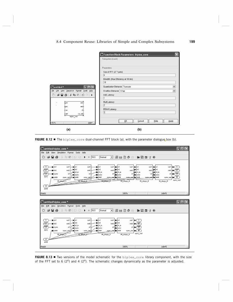
Figure 8.12 illustrates an example of a tiled cell, the biplex_core FFT block,which accepts several implementation parameters. The first parameters definethe size and precision of the FFT operator, followed by the quantization behavior(truncation or rounding) and the overflow behavior of adders (saturation orwrapping). The pipeline latencies of addition and multiplication operators arealso user selectable within the subsystem.
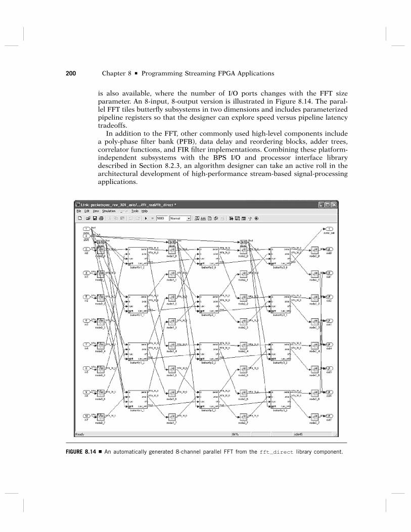
Automatically tiled library components can conditionally use different sub-systems, and can have multiple tiling dimensions. An alternative to the stream-based biplex_core block shown in Figure 8.13, a parallel FFT implementation,
8.4 Component Reuse: Libraries of Simple and Complex Subsystems 199
(a) (b)
FIGURE 8.12 � The biplex—core dual-channel FFT block (a), with the parameter dialogue box (b).
FIGURE 8.13 � Two versions of the model schematic for the biplex—core library component, with the sizeof the FFT set to 6 (26) and 4 (24). The schematic changes dynamically as the parameter is adjusted.
200 Chapter 8 � Programming Streaming FPGA Applications
is also available, where the number of I/O ports changes with the FFT sizeparameter. An 8-input, 8-output version is illustrated in Figure 8.14. The paral-lel FFT tiles butterfly subsystems in two dimensions and includes parameterizedpipeline registers so that the designer can explore speed versus pipeline latencytradeoffs.
In addition to the FFT, other commonly used high-level components includea poly-phase filter bank (PFB), data delay and reordering blocks, adder trees,correlator functions, and FIR filter implementations. Combining these platform-independent subsystems with the BPS I/O and processor interface librarydescribed in Section 8.2.3, an algorithm designer can take an active roll in thearchitectural development of high-performance stream-based signal-processingapplications.
FIGURE 8.14 � An automatically generated 8-channel parallel FFT from the fft—direct library component.
8.5 Summary 201
8.5 SUMMARY
This chapter described the use of Simulink as a common design frameworkfor both algorithm and architecture development, with an automated path toprogram FPGA platforms. This capability, combined with a rich library of high-performance parameterized stream-based DSP components, allows new appli-cations to be developed and tested quickly.
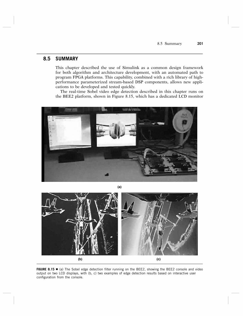
The real-time Sobel video edge detection described in this chapter runs onthe BEE2 platform, shown in Figure 8.15, which has a dedicated LCD monitor
(a)
(b) (c)
FIGURE 8.15 � (a) The Sobel edge detection filter running on the BEE2, showing the BEE2 console and videooutput on two LCD displays, with (b, c) two examples of edge detection results based on interactive userconfiguration from the console.
202 Chapter 8 � Programming Streaming FPGA Applications
connected to it. Two filtered video samples are shown, with edges displayed withand without the original source color video image.
For more information on the BPS and related software, visit http://bee2.eecs.berkeley.edu, and for examples of high-performance stream-based librarycomponents, see the Casper Project [9].
Acknowledgments This work was funded in part by C2S2, the MARCO FocusCenter for Circuit and System Solutions, under MARCO contract 2003-CT-888, and by Berkeley Wireless Research Center (BWRC) member companies(bwrc.eecs.berkeley.edu). The BEE Platform Studio development was done jointlywith the Casper group at the Space Sciences Laboratory (ssl.berkeley.edu/casper).
References[1] http://www.mathworks.com.[2] http://www.xilinx.com.[3] http://www.synplicity.com.[4] C. Chang, J. Wawrzynek, R. W. Brodersen. BEE2: A high-end reconfigurable com-
puting system. IEEE Design and Test of Computers 22(2), March/April 2005.[5] C. Chang. Design and Applications of a Reconfigurable Computing System for High
Performance Digital Signal Processing, Ph.D. thesis, University of California atBerkeley, 2005.
[6] http://www.mentor.com[7] K. Camera, H. K.-H. So, R. W. Brodersen. An integrated debugging environment
for reprogrammble hardware systems. Sixth International Symposium on Automatedand Analysis-Driven Debugging, September, 2005.
[8] A. Parsont et al. PetaOp/Second FPGA signal processing for SETI and radio astron-omy. Asilomar Conference on Signals, Systems, and Computers, November 2006.
[9] http://seti.eecs.berkeley.edu/casper.