oscillators utilizing ferroelectric-based transistors and
TRANSCRIPT

IEEE TRANSACTIONS ON ELECTRON DEVICES, VOL. 66, NO. 5, MAY 2019 2415
Oscillators Utilizing Ferroelectric-BasedTransistors and Their Coupled Dynamics
Niharika Thakuria , Atanu K. Saha, Sandeep K. Thirumala , Byunghoo Jung,and Sumeet K. Gupta, Member, IEEE
Abstract— We propose the application of ferroelectric(FE)-based transistors, viz., negative capacitance FET(NCFET) and Hysteretic ferroelectric FET (FEFET) in thedesign of coupled oscillators. The proposed oscillator uti-lizes hysteretic inverter voltage transfer characteristics,which is achieved by virtue of: 1) negative output con-ductance (NOC) in NCFETs and 2) hysteretic transfercharacteristics in FEFETs. With the aid of output-to-inputfeedback in the inverter, we show sustained oscillationswhich are controllable by the gate voltage of the feedbacktransistor (V BIAS). With focus on NCFET-based designs,we show that feedback implementation with pass transis-tor (PT) and transmission gate (TG) yields relaxation andsinusoid-like characteristics, respectively. Such behavioroffers promises for dynamically reconfiguring the oscilla-tor dynamics. We report the fundamental frequency (f ) inthe range of 12 MHz–800 MHz and 0.7 MHz–417 MHz forTG and PT implementations, respectively. We discuss howthis approach can be extended to hysteretic FEFET-baseddesigns. We also analyze coupling between two oscilla-tors considering various strengths of coupling capacitance(CCP). We establish the conditions for synchronization of fbetween the two oscillators with respect to difference in fand CCP.
Index Terms— Coupled oscillator, ferroelectric FET(FEFET), hysteresis, negative capacitance (NC), non-Boolean, Schmitt trigger.
I. INTRODUCTION
THE CMOS-based von Neumann architectures haveneared limits due to demands for increased computational
ability, scalability, and sustained power. This has led to asurge in alternative paradigms of computing such as non-Boolean/neuromorphic computation for applications involvinglearning, matching, and recognition similar to that in neu-ron [1]. Several implementations of neural networks have beenproposed among which oscillatory neuron networks (ONNs)
Manuscript received December 19, 2018; revised February 5, 2019;accepted February 22, 2019. Date of publication March 19, 2019;date of current version April 22, 2019. This work was supported byNSF under Grant 1717999 and Grant 1814756. The review of thispaper was arranged by Editor Y. Chauhan. (Corresponding author:Niharika Thakuria.)
The authors are with the School of Electrical and ComputerEngineering, Purdue University, West Lafayette, IN 47907 USA (e-mail:[email protected]; [email protected]; [email protected];[email protected]; [email protected]).
Color versions of one or more of the figures in this paper are availableonline at http://ieeexplore.ieee.org.
Digital Object Identifier 10.1109/TED.2019.2902107
are prominent [2]–[5]. This is because of the operationalsimilarities to techniques of learning in the brain, which isaccomplished by synchronization of oscillations of neuronsynapses. Many applications such as pattern matching andgraph coloring [3], [4] have been developed based on syn-chronization dynamics of oscillators.
Previously, efforts have been undertaken to design cou-pled oscillator-based systems with CMOS components [2].However, the concerns of scalability in size, power, andperformance have prevented them from coming to the fore.More recently, oscillators have been proposed with noveldevices such as those based on electron spin [6], [7], e.g., spin-torque oscillators and correlated materials [8], [9], e.g., VO2and TaOx–TiOx . While many aspects of ONN for non-Boolean/neuromorphic computing have been researched withemerging oscillators, concerns of low power, scalability, andhigh frequency in such systems continue to draw attention.
Recently, steep switching devices [9]–[11] have shownpromising solutions for the power-performance-scalabilityconflict. Among the variety of the proposed steep switchingdevices, ferroelectric (FE)-based negative capacitance (NC)FET (NCFET) [9], [10] has generated enormous interestas a replacement to CMOS due to its high-ON and low-OFF current enabling aggressive VDD scaling for logic andSRAMs [12], [16]. Another class of FE-based transistorsis hysteretic FE transistors (FEFETs) which offer severalother features [13], [14] that have guided their applicationsin low power non-volatile memories/logic and neuromorphiccomputing [15], [16].
The question, therefore, arises whether efficient oscillatorscan be enabled with FE-based transistors that can potentiallymitigate the problems associated with other technologies. If theunique properties of such transistors are ingeniously utilized torealize compact and low-power oscillators, they may result inbetter designs of coupled ONN. Recently, hysteretic FEFETshave been employed in designing coupled oscillators [16].Employing capacitors in the range of nF, these oscillatorsdisplay kHz range of fundamental frequency. However, theirfunctionality and stability for smaller capacitance need furtherexploration to ensure their utility in high performance ONNs.Moreover, hysteretic FEFETs may limit circuit performancedue to polarization switching [15] in contrast to partialpolarization switching [12] in NCFETs. Partial polarizationswitching in NCFETs results in higher speed (lower time
0018-9383 © 2019 IEEE. Personal use is permitted, but republication/redistribution requires IEEE permission.See http://www.ieee.org/publications_standards/publications/rights/index.html for more information.
2416 IEEE TRANSACTIONS ON ELECTRON DEVICES, VOL. 66, NO. 5, MAY 2019
taken to partially switch polarization) and lower energy ofswitching (since the amount of charge switched is lower).In consequence, NCFET-based oscillators may perform betterin terms of higher frequencies and energy efficiency than oscil-lators designed with hysteretic FEFET (in which polarizationswitches).
In this paper, we explore the possibility of NCFET- andFEFET-based oscillators with the focus on NCFET-baseddesigns. We utilize the negative output conductance (NOC)of NCFET for oscillator design. To give a complete picture ofimplementation of the proposed oscillator, we briefly discussthe proposed oscillator with hysteretic FEFET. This paperhighlights the following contributions.
1) We propose an oscillator utilizing FE-based transistorthat employs the Schmitt trigger action in inverter thatcan be translated to voltage controlled oscillations. SuchSchmitt trigger action is achieved by virtue of: a) NOCin NCFETs and b) hysteretic transfer characteristics ofFEFETs.
2) Oscillations are sustained by the output–input feedback.We show that the feedback can be dynamically recon-figured to obtain distinct oscillatory characteristics, viz.,relaxation or sinusoid-like dynamics.
3) We discuss device-circuit co-design of our oscillatorswith respect to thickness of FE (TFE) and voltage (VBIAS)controlling the resistance (Rf ) of the feedback path.
4) We demonstrate coupling between the oscillator pairsand discuss synchronization dynamics between twooscillators with respect to VBIAS and coupling capaci-tance (CCP).
II. MODELING AND SIMULATIONS
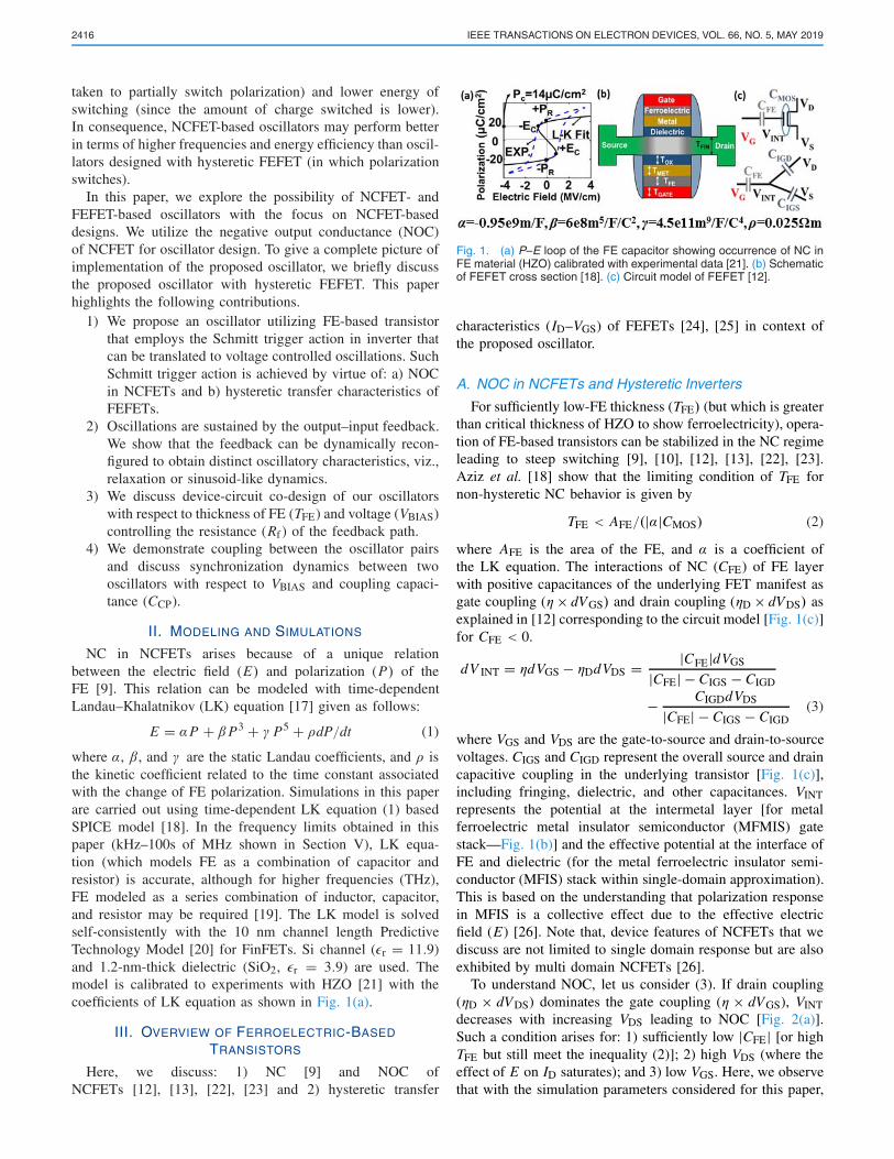
NC in NCFETs arises because of a unique relationbetween the electric field (E) and polarization (P) of theFE [9]. This relation can be modeled with time-dependentLandau–Khalatnikov (LK) equation [17] given as follows:
E = αP + β P3 + γ P5 + ρdP/dt (1)
where α, β, and γ are the static Landau coefficients, and ρ isthe kinetic coefficient related to the time constant associatedwith the change of FE polarization. Simulations in this paperare carried out using time-dependent LK equation (1) basedSPICE model [18]. In the frequency limits obtained in thispaper (kHz–100s of MHz shown in Section V), LK equa-tion (which models FE as a combination of capacitor andresistor) is accurate, although for higher frequencies (THz),FE modeled as a series combination of inductor, capacitor,and resistor may be required [19]. The LK model is solvedself-consistently with the 10 nm channel length PredictiveTechnology Model [20] for FinFETs. Si channel (�r = 11.9)and 1.2-nm-thick dielectric (SiO2, �r = 3.9) are used. Themodel is calibrated to experiments with HZO [21] with thecoefficients of LK equation as shown in Fig. 1(a).
III. OVERVIEW OF FERROELECTRIC-BASED
TRANSISTORS
Here, we discuss: 1) NC [9] and NOC ofNCFETs [12], [13], [22], [23] and 2) hysteretic transfer
Fig. 1. (a) P–E loop of the FE capacitor showing occurrence of NC inFE material (HZO) calibrated with experimental data [21]. (b) Schematicof FEFET cross section [18]. (c) Circuit model of FEFET [12].
characteristics (ID–VGS) of FEFETs [24], [25] in context ofthe proposed oscillator.
A. NOC in NCFETs and Hysteretic Inverters
For sufficiently low-FE thickness (TFE) (but which is greaterthan critical thickness of HZO to show ferroelectricity), opera-tion of FE-based transistors can be stabilized in the NC regimeleading to steep switching [9], [10], [12], [13], [22], [23].Aziz et al. [18] show that the limiting condition of TFE fornon-hysteretic NC behavior is given by
TFE < AFE/(|α|CMOS) (2)
where AFE is the area of the FE, and α is a coefficient ofthe LK equation. The interactions of NC (CFE) of FE layerwith positive capacitances of the underlying FET manifest asgate coupling (η × dVGS) and drain coupling (ηD × dVDS) asexplained in [12] corresponding to the circuit model [Fig. 1(c)]for CFE < 0.
dV INT = ηdVGS − ηDdVDS = |CFE|dVGS
|CFE| − CIGS − CIGD
− CIGDdVDS
|CFE| − CIGS − CIGD(3)
where VGS and VDS are the gate-to-source and drain-to-sourcevoltages. CIGS and CIGD represent the overall source and draincapacitive coupling in the underlying transistor [Fig. 1(c)],including fringing, dielectric, and other capacitances. VINTrepresents the potential at the intermetal layer [for metalferroelectric metal insulator semiconductor (MFMIS) gatestack—Fig. 1(b)] and the effective potential at the interface ofFE and dielectric (for the metal ferroelectric insulator semi-conductor (MFIS) stack within single-domain approximation).This is based on the understanding that polarization responsein MFIS is a collective effect due to the effective electricfield (E) [26]. Note that, device features of NCFETs that wediscuss are not limited to single domain response but are alsoexhibited by multi domain NCFETs [26].
To understand NOC, let us consider (3). If drain coupling(ηD × dVDS) dominates the gate coupling (η × dVGS), VINTdecreases with increasing VDS leading to NOC [Fig. 2(a)].Such a condition arises for: 1) sufficiently low |CFE| [or highTFE but still meet the inequality (2)]; 2) high VDS (where theeffect of E on ID saturates); and 3) low VGS. Here, we observethat with the simulation parameters considered for this paper,

THAKURIA et al.: OSCILLATORS UTILIZING FE-BASED TRANSISTORS AND THEIR COUPLED DYNAMICS 2417
Fig. 2. (a) Output (ID–VDS) characteristics of standard FET and NCFET. NCFET with TFE ≥ 7 nm shows NOC. (b) Load line of NCFET inverter forTFE (≥7 nm) at VI = VDD/2. Due to NOC for large VDS, IDS of N-NCFET lowers, and IDS of P-NCFET lowers when VDS decreases. This results inmultiple intersections. (c) VTC of NCFET-based inverter for TFE ≥ 7 nm. (d) VTC of inverter with P-FinFET and N-NCFET (TFE = 10 nm).
Fig. 3. (a) Hysteretic FEFET transfer characteristics (ID–VGS). (b) VTCof hysteretic FEFET-based inverter for TFE = 8 nm.
NOC occurs for TFE ≥ 7 nm [Fig. 2(a)] and increases withTFE [12], [23].
NOC in NCFETs leads to hysteretic inverter voltage trans-fer characteristics (VTC) [12], [13], [22] [Fig. 2(c)] whichis explained through multiple intersections in load line ofP-/N-NCFET [similar to 1, 2, and 3 as marked in Fig. 2(b)for TFE ≥ 7 nm]. Enhanced NOC with increase in TFE leadsto larger hysteresis window [∼�VM = VMP − VMN shown inFig. 2(c)] [12], [13], [22]. Also, the hysteretic VTC can beobtained in an inverter with 1-NCFET and 1-FinFET, albeitfor higher TFE (≥9 nm) [Fig. 2(d) with TFE = 10 nm]. Thisexpands the design options for our oscillator depending on thedesign target and technological capabilities.
B. Hysteretic FEFETs
In addition to NCFETs, FE-based gate stacks can be uti-lized to obtain hysteretic ID–VGS [Fig. 3(a)] in FEFETs.Experiments [24], [25] have demonstrated such characteristics,targeted toward memory/synapse designs [15], [16]. This istypically observed for TFE larger than the critical value givenby the right-hand side (RHS) of (2). Moreover, the capacitanceof the underlying transistor (CMOS) is optimized to reducethe RHS of (2) to achieve hysteresis with reasonable TFE.By proper gate work-function engineering, hysteresis can beshifted to |VGS| > 0 region [16], which proves to be helpfulin the design of FEFET-based hysteretic inverter. Such anFEFET has been demonstrated experimentally [24], [25]. Here,we analyze an inverter designed with P-/N-FEFET showinghysteretic VTC [Fig. 3(b)]. Such a design can be used for theproposed oscillator design similar to the NCFET inverter-basedoscillator design.
To sum up, hysteretic VTCs are exhibited by: 1) NCFETinverter; 2) inverter with 1-NCFET/1-FinFET; and 3) hys-teretic FEFET inverters [Figs. 2(c) and (d) and 3(b)]. How-
Fig. 4. (a) Schematic of NCFET inverter-based oscillator with PT andTG as Rf. (b) Sequence of operation of oscillatory behavior. (c) and (d)Transient waveform of oscillator with PT-/TG-NCFET as feedback resistorfor VBIAS = VDD/2 and TFE = 7 nm.
ever, the underlying mechanisms and design windows forTFE are different. While NOC in NCFET leads to hystere-sis in VTC in 1) and 2), inherent hysteretic ID–VGS inFEFETs is the prime reason for the same in 3). HystereticVTC is observed in NCFET inverter for TFE ≥ 7 nm[Fig. 2(c)] and TFE ≥ 9 nm in 1-NCFET/1-FinFET inverter[Fig. 2(d)]. For FEFET inverter, TFE ≥ 8 nm [Fig. 3(b)] alongwith other device optimizations (as described in the previousparagraph) leads to hysteretic inverter characteristics. FEFETinverters show the wider hysteresis compared to NCFETinverter or 1-NCFET and 1-FinFET inverter.
In summary, NOC in NCFETs and hysteresis in FEFETslead to the Schmitt Trigger action with two transistors com-pared to six transistors in the CMOS design [27]. This offerscompact solutions for designs based on the Schmitt trigger.In this paper, we utilize this feature for the design of low areaoscillators.
IV. NCFET OSCILLATOR
With the understanding of hysteretic NCFET inverter behav-ior, we now present the proposed oscillator. The schematicof the oscillator is shown in Fig. 4(a). Our design utilizesthe Schmitt trigger action in NCFET inverter and a feed-back between inverter input and output to obtain sustainedoscillations. Feedback resistor (R f ) can be implemented with

2418 IEEE TRANSACTIONS ON ELECTRON DEVICES, VOL. 66, NO. 5, MAY 2019
N-/P-NCFET pass transistor (denoted by PT) or NCFETtransmission gate (TG) shown in Fig. 4(a). R f can be tunedthrough the gate bias VBIAS. Feedback capacitance C f shownin Fig. 4(a) consists of two components: 1) input capacitanceof the NCFET inverter (CINV which is dependent on TFE) and2) other components, e.g., wire capacitance/fixed capacitancelumped as CDES that may be added for achieving sustainabilityof oscillations. Similarly, output capacitance Cout is represen-tative of two cumulative capacitances: 1) drain capacitanceof transistors in inverter (pull up and pull down) and PT/TG(Cdrain) and 2) any additional capacitance (CO,DES).
The operation of the proposed oscillator is described asfollows and is illustrated in Fig. 4(b). To begin with, let thefeedback path (PT/TG) be open (VBIAS = 0 V), input voltageVI = 0 V, and output voltage VO = VDD. When the feedbackpath is established (VBIAS > 0), VI starts to increase dueto charging of C f by current I f i [Fig. 4(b)]. This continuestill VI reaches VMP, at which point, VO flips to 0 V. Notethat, VMP refers to VI for which VO trips from VDD → 0[Fig. 2(c)]. Now, the current direction through the feedbackpath reverses (I f o flows from VI to VO) and therefore, C f
starts to discharge VI. After VI reaches VMN, VO returns toVDD. VMN refers to the input voltage of the inverter (VI) forwhich the output voltage (VO) changes from 0 → VDD. Thisprocess repeats to generate sustained oscillations, which is aresult of VI transitioning between VMP and VMN.
Fig. 4(c) and (d) shows the waveforms for the PT(N-NCFET) and TG-based implementations of R f . WhileFig. 4(c) shows relaxation-type characteristics, the oscilla-tions shown in Fig. 4(d) are sinusoid-like. To understandthis behavior, let us begin our discussion with PT-based R f .The relaxation-type waveform [Fig. 4(c)] results due to theasymmetry in transition time for VMP → VMN and VMN →VMP. This can be further explained by analyzing the insetof Fig. 4(c). Let VO = VDD and VI = VDD/2. VO chargesC f with current I f i until VI = VMP is reached through PTfeedback. It is evident from the inset of Fig. 4(c) (marked asT1) that a large time constant (τ f ) of PT is involved in thisprocess. Inspection of the bias conditions of the PT suggeststhat due to small VGS and VDS (VBIAS(G) ∼ VDD/2 (or VMN),VDD/2 < VI(S) < VMP, and VO(D) ∼ VDD), it conductswith large R f . When VI = VMP, the inverter transitionsto low logic output (VO = 0). We refer to this transition(VI = VMN → VMP) as T1. Now, the feedback PT will actto discharge VI due to I f o flowing from VI to VO. It is biasedat VGS = VDD/2 and VDS ∼ VDD/2 (VBIAS(G) = VDD/2,VO(S) ∼ 0, and VMP < VI(D) < VMN) indicating a low R f
state. Hence, VI transitioning phase (VI = VMP → VMN) ofthe oscillator as T2. Again VO discharges with high R f andτ f until VI reaches VMP (T1 transition phase). Repetition ofT1 and T2 results in oscillations.
Due to much higher transition time of VMN → VMP(tMN→MP) than that for VMP → VMN(tMP→MN), relaxationoscillations are observed. On the other hand, TG-based imple-mentation of R f displays symmetric sinusoid-like character-istics. In this configuration, we apply VBIAS at the gate ofthe N-NCFET of the TG and fix the gate of the P-NCFETto VDD/2 [Fig. 4(a)]. We know from the discussion of PT
R f -based oscillator that in T1, R f due to PT only is large.However, in TG implementation due to the bias conditionsof P-NCFET: |VGS| = |VDS| = VDD/2 (VBIAS(G) = VDD/2,VO(S) ∼ VDD, and VI(D) ∼ VDD/2), low R f state is achievedin T1. During T2, low feedback resistance condition prevailsby virtue of N-NCFET in T2 (similar to the PT-based design).Thus, TG feedback implementation ensures low R f duringVMN → VMP and VMP → VMN. This results in almost sym-metric transition for input charging and discharging, yielding“sinusoid-like” oscillator [Fig. 4(d)]. The same argument holdsin case of an oscillator with purely resistive feedback thatshows “sinusoid-like” characteristics.
Note that, the run-time reconfiguration of the oscillationdynamics between the relaxation-type and sinusoid-like canbe enabled using bias of P-NCFET in the feedback path.If gate of P-NCFET is VDD/2, the feedback acts as a TGyielding sinusoid-like characteristics while by setting it to VDD(P-NCFET is OFF), the feedback is reduced to PT, leadingto relaxation behavior. Thus, the proposed oscillator allowsdynamic reconfigurability while offering a more compactimplementation compared to standard CMOS designs. Theproposed design can also be realized with hysteretic FEFETs(see Section VI) although our focus is on non-hystereticNCFETs (exhibiting NOC) due to their faster and more energyefficient nature [12].
V. ANALYSIS OF NCFET OSCILLATOR
The fundamental frequency ( f ) for TG and PT is734 MHz and 13.4 MHz for VDD = 0.4, VBIAS = VDD/2,C f = 5.2 fF, Cout = 0.24 fF, and TFE = 7 nm. Recall fromFig. 2(c) that for TFE ≥ 7 nm NCFET inverter shows thehysteretic VTC that is utilized for our oscillator design (referto Section IV). More details about calculation of C f and Coutare provided in Section V-C. It is noteworthy that TG-baseddesign yields higher f (55X) than PT implementation due tolower charging time (tMP→MN) in the former.
We further explore the performance of the proposed oscilla-tor to understand the impact of various device-circuit charac-teristics. The oscillation frequency f depends on two factors:1) time constant (τ f = R f C f ) of the feedback path and2) hysteresis in VTC (�VM ) of inverter. An increase inτ f lowers f due to larger charging/discharging time of VI.Independently, an increase in �VM implies increase in timefor VMN → VMP transition and vice versa due to largervoltage swing, yielding lower f . With these factors in mind,we analyze the oscillator characteristics for different designparameters.
A. Voltage Controllability of Frequency
Here, we discuss voltage (VBIAS) controllability of f forPT- and TG-based designs. By increasing VBIAS, we mod-ulate τ f (R f and C f ) while maintaining a constant �VM .An increase in VBIAS leads to: 1) lower R f and 2) higherC f . To understand this further, note that, in the NC regimeof NCFET, the effective gate capacitance of device (C f g) isa combination of the 1) NC-induced amplification (η) and 2)capacitance of the underlying transistor (CIGD + CIGS) given

THAKURIA et al.: OSCILLATORS UTILIZING FE-BASED TRANSISTORS AND THEIR COUPLED DYNAMICS 2419
Fig. 5. Variation of NCFET oscillator frequency f with (a) feedback control voltage VBIAS, (b) FE thickness TFE, and (c) and (d) Comparison of f ofNCFET oscillator versus CMOS oscillator for varying VBIAS.
by C f g = η × (CIGS + CIGD) [12]. As VGS rises, η increases(in the range of VGS = 0–0.4 V for LK coefficients in thispaper). Also, CIGD + CIGS increases with VGS. Both thesefactors yield higher C f g . The details of this are in [12]. Butdecrease in R f dominates over increase in C f g in both PT andTG design, since C f is composed of components other thanC f g , e.g., CDES (see Section IV). Note that, C f g contributes toCINV (from Section IV). Hence, an increase in f with increasein VBIAS is achieved.
Having understood the impact of VBIAS on f , let us nowanalyze the range of VBIAS and corresponding f of successfuloscillatory operation [Fig. 5(a)]. The PT oscillator successfullyoscillates when 0.12 V < VBIAS < 0.29 V. For VBIAS <0.12 V, the oscillations cannot be sustained since PT fails toturn on to establish the feedback path. When VBIAS > 0.29 V,τ f is exceedingly small and the delay associated with thefeedback is smaller than the delay in inverter switching. Thisleads to degradation of the input voltage with oscillationscompletely damping after some time. On the other hand, forTG design, the range of VBIAS for which oscillations areachieved is 0 V < VBIAS < 0.26 V. We explain the differencebetween TG and PT oscillator design in this regard as follows.Due to fixed biasing of P-NCFET gate at VDD/2 [Fig. 4(a)],a feedback path is present for all VBIAS in the TG. Therefore,even when VBIAS is small (<0.12 V), TG-based design yieldsoscillation (whereas PT-based oscillator becomes nonfunc-tional). However, at high VBIAS (>0.26 V), the concerted effectof N-NCFET and P-NCFET in TG makes τ f comparableto the inverter delay leading to unsustained oscillations inthe TG design. On the other hand, the PT design allowsgreater flexibility in the high VBIAS region due to higherfeedback delay. Therefore, while tuning range of PT designis 0.12 V < VBIAS < 0.29 V, for TG implementation, thisrange is 0 V < VBIAS < 0.26 V. f in the respective rangescan be tuned between 12 MHz and 800 MHz for TG and0.7 MHz–417 MHz for PT implementations, respectively. Itmay be reiterated that in addition to VBIAS-controlled f ,the oscillation type can also be dynamically reconfigured usingthe gate bias of the P-NCFET, which could open avenues fornew applications.
Finally, we compare the performance of the proposedNCFET oscillator to the CMOS Schmitt trigger-based oscilla-tor (also mentioned in Section III). f of CMOS TG oscillatoris ∼5X lower than NCFET TG type [Fig. 5(c)], whereasCMOS PT oscillator is ∼10X lower than NCFET PT-basedoscillator [Fig. 5(d)]. Lower f is due to larger �VM in
CMOS-based Schmitt trigger and higher R f of the stan-dard FinFET-based feedback compared to R f of NCFETfeedback.
B. Impact of TFE and Cf on Frequency (f)
Let us begin by analyzing the impact of FE thick-ness TFE on f . Increase in TFE results in: 1) higher ID[Fig. 2(a)] or lower R f ; 2) larger �VM [Fig. 2(c)]; and3) larger gate capacitance of the NCFET due to negativeCFE [12], which increases C f . To explain the overall impact,we compare PT- and TG-based designs [Fig. 4(a)]. While forPT oscillator, increase in TFE reduces f , TG-based designshows an increasing trend [Fig. 5(b)]. We explain these trendsas follows.
Let us begin with PT-based feedback. Recall from the priordiscussion in Section IV that VBIAS = VDD/2 for PT results inlow f of the oscillator due to large tMN→MP. For VDD = 0.4 V,VBIAS = 0.2 V and PT are biased in the near-threshold region,and its drive strength is low. Hence, although ID increases withincrease in TFE [Fig. 2(b)], the increase in �VM [Fig. 2(c)],and C f is much more impactful. In other words, in PT-basedoscillator, the effect of �VM dominates over increase in IDresulting in decrease in f with increasing TFE.
Considering the case of a TG feedback-based oscillator, forVBIAS = VDD/2 either P-NCFET/N-NCFET ensures that R f isalways low (or the feedback NCFET is strong as discussed inSection IV). More specifically, since the feedback transistor isnow operating at VDS ≥ VDD/2, ID–VDS [Fig. 2(a)] suggestssignificant increase in ID with increase in TFE for the said biascondition. Hence, for the same increase in �VM , the reductionin R f with TFE increase is more effective in TG compared toPT due to the concerted action of P- and N-devices in theformer. Thus, for TG design, decrease in R f dominates over�VM increase leading to an increase in f with increasing TFE.
As TFE increases from 7 nm to 9 nm, f decreases by5.5X (from 13.3 to 2.4 MHz) in PT implementation, whereasf increases by 1.6X (734 MHz–1190 MHz) as shown inFig. 5(b).
Since τ f also affects C f , (due to CINV described inSection IV), an independent analysis of the dependenceof oscillation dynamics on C f becomes important. This isbecause C f not only depends on TFE (the overall effect ofwhich we have already discussed) but may also be tuned byoptimizing other components and even adding an additionalcapacitor (CDES). It may be noted that since the primarydriving mechanism for oscillations in our design is repeated

2420 IEEE TRANSACTIONS ON ELECTRON DEVICES, VOL. 66, NO. 5, MAY 2019
Fig. 6. Power spectrum of NCFET TG oscillator for (a) low (5.2 fF)feedback capacitance Cf and (b) high (1 pF) Cf.
Fig. 7. Power spectrum of oscillator (a) and (b) with PT as Rf and (c)and (d) TG as Rf for Cf = 1 pF in both cases.
transitions of VI between VMN and VMP (which, in turn,depends on charging/discharging of C f , as explained earlier),C f plays a more important role in determining the characteris-tics of voltage-controlled oscillations than Cout. Since both C f
and Cout show the similar trends with respect to f , we focuson analyzing the dependence of f on C f . As expected, fdecreases from 13.4 MHz to 0.12 MHz as C f increases from5.2 fF to 1 pF for TG implementation. For TG, f decreasesfrom 734 MHz to 16 MHz as C f increases from 5.2 fF to 1 pF.Simultaneously, an increase in C f leads to better sustenanceof oscillations for a wider range of design parameters. Thus,depending on application requirements (higher f /robustness),proper C f can be chosen. To analyze the impact of C f onthe robustness of oscillator, we examine the power spectrumin Section V-C.
C. Output Power Spectrum
The output power spectrum is a widely accepted measureof robustness to noise [28]. A higher peak indicates moreresilience. Here, the robustness of the oscillator is a functionof C f (comprising CINV and CDES described in Section IV).For NCFET TG design at TFE = 7 nm and VBIAS =0.2 V, C f = 5.2 fF (CINV = 0.2 fF, CDES = 5 fF, andC f = 5.2 fF) results in a peak power of −20 dB [Fig. 6(a)] at734 MHz, while for C f = 1 pF (CINV = 0.2 fF, CDES = 1 pF,and C f ∼ CDES, since CINV � CDES), the observed peakpower is −18 dB at 16 MHz [Fig. 6(b)]. Thus, higher C f
enhances robustness of the oscillator. Note that, oscillationsare sustained with desirable power (≤−20 dB) when fixedcapacitances CDES ≥ 5 fF and CO,DES ≥ 0.1 fF. In addition,CINV (averaged over voltage) is 0.2–0.25 fF for TFE =7–8 nm (hence C f = 5.2 fF) and capacitance at the inverteroutput = 0.14 fF (total Cout = 0.24 fF).
To reinforce the understanding of power spectrum of theproposed designs, we analyze the power spectrum of theproposed oscillators (PT and TG) for a different TFE. Notethat CINV depends on TFE. Fig. 7 shows the sharp and narrow
Fig. 8. (a) Schematic of FEFET (TFE = 8 nm) inverter-based oscillatorwith P-/N-FEFET and FinFET-based PT/TG feedback (Rf). (b) Variationof oscillator f with VBIAS. (c) and (d) Transient waveform of FEFEToscillator with PT/TG feedback.
peaks in the spectrum. The maximum peak values are −39 dBand −18 dB for PT and TG (TFE = 7 nm) oscillator [Fig. 7(a)and (c)], respectively. Due to the relaxation-type behaviorof the PT-based oscillators, distinct sidelobes in the powerspectrum are observed [28]. Furthermore, on increasing TFE,the spectrum peaks at lower oscillation frequency ( f ) for thePT design. For the TG implementation, increasing TFEshowsincrease in robustness [Fig. 7(c) and (d)]. The discussionsin this section related to frequency and power spectrumconsidering device–circuit parameters can guide optimizationof the proposed oscillator depending on the design targets.
To conclude this discussion, we compare this paper with theprevious reporting of FEFET oscillator [16]. For proper com-parisons, we obtain the coercive field and remnant polarizationof FE and capacitances (∼8 nF) from [16] and redesign ouroscillator with the same parameters. However, since the valueof viscosity coefficient (ρ) is not available in [16], we performsimulation for our design using a rather conservative valueρ = 2.5 ·cm (compared to 0.18 ·cm reported in [19]). Forsuch a value of ρ, the polarization switching rates of the orderof GHz are expected. Since oscillators in this comparativestudy show f in KHz-MHz (due to nF of capacitance),the influence of ρ on f is negligible. The oscillator in [16]shows maximum f = 12 kHz and −20 dB power with 8 nFcapacitance. In comparison, at C f = 8 nF, the proposedTG oscillator displays a more robust design with −6.3 dBpower at f = 6.72 kHz. At iso-power of −20 dB, the TGimplementation displays higher f (=15 MHz with C f = 1 pF)compared to 12 kHz in [16]. The referred design does notthrow light on its performance at lower capacitance; hence, itshigh f operation needs to be further examined. On the otherhand, our design can work for capacitances of the order ofseveral fF. In terms of voltage controllability, the maximumreported range in [16] is 0.2–0.36 V ( f = 5 kHz − 12 kHz)compared to 0–0.26 V ( f = 80 kHz–20 MHz). Moreover, ourdesign displays dynamic reconfigurability between oscillationtypes while incurring an overhead of two more NCFETs (forthe TG design) compared to the referred design in [16].Finally, the proposed oscillator can be designed with hys-teretic FEFETs as well as non-hysteretic NCFETs (exhibitingNOC), and is, therefore, more generic than [16], which islimited to the hysteretic regime. While the focus of this paperis on NCFET-based oscillators, we briefly discuss how the

THAKURIA et al.: OSCILLATORS UTILIZING FE-BASED TRANSISTORS AND THEIR COUPLED DYNAMICS 2421
Fig. 9. Schematic of NCFET TG coupled oscillator for (a) input–inputcoupling and (b) output–output coupling.
proposed technique can also be applied to hysteretic FEFETsin Section VI.
VI. FEFET-BASED OSCILLATOR
Hysteretic FEFET-based inverter can show hysteretic VTC[Fig. 3(b)] for TFE ≥ 8 nm (refer to Section III). Therefore,oscillations can be sustained by providing a feedback fromoutput to input [Fig. 8(a)] similar to that in NCFET oscillator.Here, we analyze the oscillator with FinFET-based feedbackdesigned with PT and TG. Voltage controllability of f isachieved through VBIAS [Fig. 8(b)]. Also, reconfigurabilityis observed between the pulse-like [Fig. 8(c)] and relaxationcharacteristics [Fig. 8(d)] for TG and PT designs. The pulse-like waveforms of FEFET TG are seen due to sharp polariza-tion switching as opposed to partial polarization switching inNCFET TG which gives rise to sinusoid-like waveforms. PTimplementation shows oscillations for VBIAS = 0.12–0.5 Vwith f = 5.36 Hz–0.97 MHz, while for TG designoscillations are observed for VBIAS = 0.0–0.5 V withf = 0.9 MHz–1.1 GHz [Fig. 8(b)]. Comparing Fig. 8(b) withFig. 5(a), we observe that both PT and TG NCFET oscillatorshow higher f (even at lower VDD) than respective PT/TGimplementation of FEFET oscillator due to polarizationswitching in the latter.
VII. COUPLING BETWEEN NCFET-BASED
OSCILLATORS
In non-Boolean computation, coupled oscillators providesolution to complex problems like pattern matching [3]. In pat-tern matching, the extent of synchronization between oscilla-tors is studied to determine the closeness of two patterns. Theinput of one of the oscillators corresponds to the input pattern,and the input to the other is the pattern to be identified.
Considering the importance of coupled oscillators for suchapplications, we now discuss the coupling dynamics betweenthe two oscillators (Fig. 9) with a focus on NCFET designs.We consider natural frequencies f1 and f2 corresponding toinputs VBIAS1 and VBIAS2, respectively.
Coupling is achieved via a coupling capacitor (CCP) ineither input–input (VI1–VI2) [Fig. 9(a)] or output–output(VO1–VO2) [Fig. 9(b)] configurations. We show that couplingof VI1–VI2 results in out-of-phase (180◦) frequency locking.Interestingly, frequency locking is in-phase (0◦) for VO1–VO2coupling.
Let us start our discussion with TG oscillators for VI1–VI2coupling. Before coupling, we set the fundamental frequenciesf1 = 734 MHz and f2 = 760 MHz corresponding to
Fig. 10. Transient waveform and phase map for (a) and (b) CCP = 0.5 fFand (c) and (d) CCP = 5 fF. (e) Synchronization map of the oscillator forVI1–VI2 coupling in NCFET TG oscillator.
Fig. 11. (a) and (b) Phase map for CCP = 0.5 fF and CCP = 10 fF.(c) Synchronization map of the oscillator for NCFET PT VI1–VI2 coupledoscillator.
Fig. 12. (a)–(c) VO1–VO2 coupling phase map for CCP = 5 fF and 10 fFand synchronization map of NCFET PT oscillators. (d)–(f) Phase map forCCP = 0.1 fF and 5 fF and synchronization map of NCFET TG oscillators.
VBIAS1 = 0.2 V and VBIAS2 = 0.22 V. Hence, boththe waveforms are unsynchronized in frequency and phase.By introducing CCP = 5 fF, the oscillators become out-of-phase frequency locked with synchronized frequency of fS =360 MHz [Fig. 10(c)]. Once the synchronization is achieved,the relative phase of the oscillators can be modulated via CCP.Correspondingly, the transition of the lobes in the phase mapof the synchronized outputs indicates the modulation in phase[Fig. 10(d)]. When CCP = 0.5 fF is small, it represents anunsynchronized state [Fig. 10(a)] without any fixed trajectoryin the phase map [Fig. 10(b)]. The extent of synchronizationof the two oscillators depends on the strength of the coupling

2422 IEEE TRANSACTIONS ON ELECTRON DEVICES, VOL. 66, NO. 5, MAY 2019
TABLE ICOMPARISON OF EMERGING OSCILLATORS FOR NON-BOOLEAN APPLICATION
and how far apart f1 and f2 are set. It is already known to thereader that, in this paper, f is the voltage controlled throughVBIAS. Hence, we study the limits of synchronization in termsof coupling strength and frequency difference by plotting CCPversus VBIAS2, while VBIAS1 is constant in Fig. 10(e). This plotprovides the information about the required coupling strengthas a function of �VBIAS = |VBIAS2 − VBIAS1|. The range of� f (= f1 − f2) or �VBIAS for which synchronization can beachieved also increases with CCP, as shown in Fig. 10(e).
In NCFET PT feedback oscillators, synchronization isachieved for CCP ∼ 10 fF which is reflected as fixed lobesin the phase map in the inset of Fig. 11(b). At low couplingstrength (CCP ∼ 0.5 fF), multiple paths in the phase map [insetof Fig. 11(a)] are observed indicating the unsynchronized state.Fig. 11(c) shows that CCP > 20 fF determines the rangeof VBIAS2 over which synchronization is achieved. In thiscase, VBIAS2 = 0.14–0.26 V represents the synchronized state.The range of �VBIAS for which frequency synchronization isachieved is smaller for PT oscillator than TG oscillator.
Here, we explore synchronization dynamics of in-phasecoupling in VO1–VO2. PT and TG oscillators show the unsyn-chronized state for CCP = 5 fF (with multiple lobes) and0.1 fF [Fig. 12(a) and (d)], respectively. By increasing CCPto 10 fF for PT [Fig. 12(b)] and 5 fF for TG [Fig. 12(e)],synchronization is achieved. Synchronization is achieved forVBIAS2 = 0.14–0.26 V in PT oscillator [Fig. 12(c)] andVBIAS2 = 0–0.26 V in TG oscillator [Fig. 12(f)] whenCCP > 20 fF for both cases. Again, TG shows greater voltagecontrollability.
VIII. DISCUSSION
We perform a comparative performance analysis of theproposed design with other emerging nano-oscillators used fornon-Boolean application (Table I). CMOS ring oscillator cir-cuits prove as representative systems for exploration of oscil-lators in the context of non-Boolean computing [29]. Althoughsome of the emerging oscillators show high scalability, theysuffer from the requirement of high bias current (mA) [6],low frequency ( f ) at low sense voltage [8], [9], and provide
other challenges with regard to material endurance, thermalstability, and nonlinearity in the electrical behavior [5], [7], [8].The proposed technique achieves competitive frequencies ofoscillation (compared with other emerging technologies) alongwith low voltage operation. By properly defining a designspace involving transistor sizing and TFE, simultaneous controlover frequency and operating voltage can be achieved for theproposed oscillator. Our design targets low power compactdesign of oscillators with voltage tunability and reconfigurabledynamics for non-Boolean computing.
It may be noted that previously negative differential resis-tance (NDR) which is similar to NOC has been utilized indesigns other than oscillators (for instance, SRAMs [30]).In NDR-based SRAMs, there has been discussion on noiseand stability challenges. However, such issues and designneeds of SRAMs are different from the requirements inoscillator design. The issue of noise affecting storage nodeand voltage retention in NDR-based SRAMs is not directlyapplicable for oscillators since in the latter, the ease ofswitching between states is desirable for oscillations (unlikeSRAMs where the state must be stable during read). It may bementioned, however, that other sources of noise and variationsin both NCFET (with NOC) and hysteretic FEFET oscillatorneed to be properly analyzed (as with oscillator implemen-tations based on other technologies as well). Such noise andvariations can affect frequency fluctuation, increasing phasenoise. The proposed oscillator is robust to noise since itspeak power is < −20 dB at its operating frequency. ForFE-based oscillators (such as our design and that in [16]), onetechnological challenge will be the control of grain/domainvariability in the FE, which needs to be addressed not just foroscillator designs but other applications of NCFET/FEFETsas well.
IX. CONCLUSION
In this paper, we proposed a dynamically reconfigurableNCFET/FEFET oscillator. The proposed NCFET oscillatordesign is based on NOC of NCFETs, while the FEFEToscillator utilizes hysteretic transfer characteristics of FEFETs.Both these features lead to hysteretic inverter characteristics.
THAKURIA et al.: OSCILLATORS UTILIZING FE-BASED TRANSISTORS AND THEIR COUPLED DYNAMICS 2423
Exploiting such Schmitt trigger action in the inverter and withthe aid of output–input feedback, sustained oscillations areachieved in the proposed design. We demonstrate reconfig-urability and distinct relaxation and sinusoid-like oscillationsby employing PT and TG feedback in the NCFET oscillator.Voltage controllability of f is achieved through the gate biasof the feedback transistor. We also show how the proposedoscillators can be coupled to achieve frequency synchro-nization, which can lead to new applications of FE-basedtransistors in non-Boolean computing.
REFERENCES
[1] D. S. Modha, R. Ananthanarayanan, S. K. Esser, A. Ndirango,A. J. Sherbondy, and R. Singh, “Cognitive computing,” Commun. ACM,vol. 54, no. 8, pp. 62–71, Aug. 2011. doi: 10.1145/1978542.1978559.
[2] T. Shibata, R. Zhang, S. P. Levitan, D. E. Nikonov, and G. I. Bourianoff,“CMOS supporting circuitries for nano-oscillator-based associativememories,” in Proc. 13th Int. Workshop Cellular Nanosc. Netw.Appl. (CNNA), Aug. 2012, pp. 1–5. doi: 10.1109/CNNA.2012.6331473.
[3] F. C. Hoppensteadt and E. M. Izhikevich, “Pattern recognition via syn-chronization in phase-locked loop neural networks,” IEEE Trans. NeuralNetw., vol. 11, no. 3, pp. 734–738, May 2000. doi: 10.1109/72.846744.
[4] C. W. Wu, “Graph coloring via synchronization of coupled oscillators,”IEEE Trans. Circuits Syst. I. Fundam. Theory Appl., vol. 45, no. 9,pp. 974–978, Sep. 1998. doi: 10.1109/81.721263.
[5] S. Kaka, M. R. Pufall, W. H. Rippard, T. J. Silva, S. E. Russek,and J. A. Katine, “Mutual phase-locking of microwave spin torquenano-oscillators,” Nature, vol. 437, pp. 389–392, Sep. 2005. doi:10.1038/nature04035.
[6] G. Csaba et al., “Spin torque oscillator models for applicationsin associative memories,” in Proc. 13th Int. Workshop Cellu-lar Nanosc. Netw. Appl., Turin, Italy, Aug. 2012, pp. 1–2, doi:10.1109/CNNA.2012.6331474.
[7] N. Shukla, W.-Y. Tsai, M. Jerry, M. Barth, V. Narayanan, and S. Datta,“Ultra low power coupled oscillator arrays for computer vision appli-cations,” in Proc. IEEE Symp. VLSI Technol., Honolulu, HI, USA,Jun. 2016, pp. 1–2, doi: 10.1109/VLSIT.2016.7573439.
[8] A. A. Sharma, J. A. Bain and J. A. Weldon, “Phase coupling and controlof oxide-based oscillators for neuromorphic computing,” IEEE J. Explor.Solid-State Comput. Devices Circuits, vol. 1, pp. 58–66, Dec. 2015. doi:10.1109/JXCDC.2015.2448417.
[9] S. Salahuddin and S. Datta, “Use of negative capacitance to providevoltage amplification for low power nanoscale devices,” Nano Lett.,vol. 8, no. 2, pp. 405–410, Dec. 2008. doi: 10.1021/nl071804g.
[10] A. I. Khan et al., “Negative capacitance in a ferroelectric capacitor,”Nature Mater, vol. 14, no. 2, pp. 182–186, Dec. 2015.
[11] H. Lu and A. Seabaugh, “Tunnel field-effect transistors: State-of-the-art,” IEEE J. Electron Devices Soc., vol. 2, no. 4, pp. 44–49, Jul. 2014.doi: 10.1038/nmat4148.
[12] S. Gupta, M. Steiner, A. Aziz, V. Narayanan, S. Datta, and S. K. Dupta,“Device-circuit analysis of ferroelectric FETs for low-power logic,”IEEE Trans. Electron Devices, vol. 64, no. 8, pp. 3092–3100, Aug. 2017.doi: 10.1109/TED.2017.2717929.
[13] T. Dutta, G. Pahwa, A. R. Trivedi, S. Sinha, A. Agarwal, andY. S. Chauhan, “Performance evaluation of 7-nm node negative capaci-tance FinFET-based SRAM,” IEEE Electron Device Lett., vol. 38, no. 8,pp. 1161–1164, Aug. 2017. doi: 10.1109/LED.2017.2712365.
[14] S. L. Miller and P. J. McWhorter, “Physics of the ferroelectric non-volatile memory field effect transistor,” J. Appl. Phys., vol. 72, no. 12,pp. 5999–6010, Sep. 1992. doi: 10.1063/1.351910.
[15] D. Wang, S. George, A. Aziz, S. Datta, V. Narayanan, and S. K. Gupta,“Ferroelectric transistor based non-volatile flip-flop,” in Proc. Int. Symp.Low Power Electron. Design, Aug. 2016, pp. 10–15. doi: 10.1145/2934583.2934603.
[16] Z. Wang, S. Khandelwal, and A. I. Khan, “Ferroelectric oscillators andtheir coupled networks,” IEEE Electron Device Lett., vol. 38, no. 11,pp. 1614–1617, Nov. 2017. doi: 10.1109/LED.2017.2754138.
[17] T. K. Song, “Landau-Khalatnikov simulations for ferroelectric switchingin ferroelectric random access memory application,” J. Korean Phys.Soc., vol. 46, no. 1, pp. 5–9, Jan. 2005.
[18] A. Aziz, S. Ghosh, S. Dutta, and S. K. Gupta, “Physics-based circuit-compatible SPICE model for ferroelectric transistors,” IEEE ElectronDevice Lett., vol. 37, no. 6, pp. 805–808, Jun. 2016. doi: 10.1109/LED.2016.2558149.
[19] K. Chatterjee, A. J. Rosner, and S. Salahuddin, “Intrinsic speedlimit of negative capacitance transistors,” IEEE Electron Device Lett.,vol. 38, no. 9, pp. 1328–1330, Sep. 2017. doi: 10.1109/LED.2017.2731343.
[20] (2016). Arizona State University Predictive Technology Models.[Online]. Available: http://ptm.asu.edu/
[21] M. Kobayashi, N. Ueyama, K. Jang, and T. Hiramoto, “Experimen-tal study on polarization-limited operation speed of negative capaci-tance FET with ferroelectric HfO2,” in IEDM Tech. Dig., Dec. 2016,pp. 12.3.1–12.3.4. doi: 10.1109/IEDM.2016.7838402.
[22] J. Seo, J. Lee, and M. Shin, “Analysis of drain-induced barrier risingin short-channel negative-capacitance FETs and its applications,” IEEETrans. Electron Devices, vol. 64, no. 4, pp. 1793–1798, Apr. 2017.doi: 10.1109/TED.2017.2658673.
[23] G. Pahwa et al., “Analysis and compact modeling of negative capac-itance transistor with high ON-current and negative output differ-ential resistance—Part II: Model validation,” IEEE Trans. ElectronDevices, vol. 63, no. 12, pp. 4986–4992. Dec. 2016. doi: 10.1109/TED.2016.2614436.
[24] S. Dasgupta et al., “Sub-kT/q switching in strong inversion inPbZr0.52Ti0.48O3 gated negative capacitance FETs,” IEEE J. Explor.Solid-State Comput. Devices Circuits, vol. 1, pp. 43–48, Dec. 2015.doi: 10.1109/JXCDC.2015.2448414.
[25] A. I. Khan et al., “Negative capacitance in short-channel FinFETs exter-nally connected to an epitaxial ferroelectric capacitor,” IEEE ElectronDevice Lett., vol. 37, no. 1, pp. 111–114, Jan. 2016. doi: 10.1109/LED.2017.2754138.
[26] A. K. Saha, P. Sharma, I. Dabo, S. Datta, and S. K. Gupta, “Ferroelectrictransistor model based on self-consistent solution of 2D Poisson’s,non-equilibrium Green’s function and multi-domain Landau Khalat-nikov equations,” in IEDM Tech. Dig., Dec. 2017, pp. 13.5.1–13.5.4.doi: 10.1109/IEDM.2017.8268385.
[27] J. M. Rabaey. Digital Integrated Circuits: A Design Perspective.Upper Saddle River, NJ, USA: Prentice-Hall, 1996.
[28] B. Razavi, “A study of phase noise in CMOS oscillators,” IEEE J. Solid-State Circuits, vol. 31, no. 3, pp. 331–343, Mar. 1996. doi: 10.1109/4.494195.
[29] Y. Fang, C. N. Gnegy, T. Shibata, D. Dash, D. M. Chiarulli andS. P. Levitan, “Non-Boolean associative processing: Circuits, sys-tem architecture, and algorithms,” IEEE J. Explor. Solid-StateComput. Devices Circuits, vol. 1, pp. 94–102, Dec. 2015. doi:10.1109/JXCDC.2015.2507863.
[30] J. P. A. van der Wagt, “Tunneling-based SRAM,” Proc. IEEE, vol. 87,no. 4, pp. 571–595, Apr. 1999. doi: 10.1109/5.752516.