optical serdes test interface for high-speed and parallel
TRANSCRIPT

Optical SerDes Test Interface for High-Speed and Parallel Testing
Sanghoon Lee, Ph. DSejang Oh,
Kyeongseon Shin,Wuisoo Lee
Memory Division, SAMSUNG ELECTRONICS
June 7-10, 2009San Diego, CA

June 7 to 10, 2009June 7 to 10, 2009 IEEE SW Test WorkshopIEEE SW Test Workshop 2/222/22
Why Optical Interface ?• High speed up to 10GHz, Significant scalability
• Smaller cross-sectional area than electrical cable or trace.
• Immune to electromagnetic interference → Impedance matching not needed
[T. Okayasu, et al., JLT, vol. 22, no. 9, Sept. 2004]
Optical
Path
Electrical
Path
Optical
Path
Electrical
Path
DUT1
DUT2
Electrical signal
Electrical stub
Reflection
DUT1
DUT2
Optical signal
Optical coupler
Opt.RX
Opt.RX

June 7 to 10, 2009June 7 to 10, 2009 IEEE SW Test WorkshopIEEE SW Test Workshop 3/223/22
Contents1. Introduction
2. Three optical Issue in Test Interface
3. Proposed Optical SerDes Test System
4. 3D Electromagnetic Board Simulation
5. Measurement and Analysis
6. Summary

June 7 to 10, 2009June 7 to 10, 2009 IEEE SW Test WorkshopIEEE SW Test Workshop 4/224/22
Introduction
NeedleDUT (Wafer)Probe Card
MainFrame
PCB
Optical Test Interface
• Basic concept– Optical Interface is applied onto PCB of Probe Card
• For what ?– More high-speed Test– Scalability for expansion of ATE’s resource– Good PCB noise immunity

June 7 to 10, 2009June 7 to 10, 2009 IEEE SW Test WorkshopIEEE SW Test Workshop 5/225/22
Optical TX
Optical fiber
DUT
CLK
RAS
CAS
A0
A1
DQ0
DQ1
Optical RX
1
40
39
3
2
4
1
40
39
3
2
4
ATE
CLK
RAS
CAS
A0
A1
DQ0
DQ1
ATE
CLK
RAS
CAS
A0
A1
DQ0
DQ1
Optical Issue in Test Interface (1)• Many of optical modules required (Optical TX/RX + Fiber)
– Total of about 80 optical modules including transmitter and receiverwhen evaluate a single memory chip with only write operation.
DUT
CLK
RAS
CAS
A0
A1
DQ0
DQ1
ATE
CLK
RAS
CAS
A0
A1
DQ0
DQ1
ATE
CLK
RAS
CAS
A0
A1
DQ0
DQ1
Optical TX Optical RX
SerDes SerDes
Parallel
to
Serial
Parallel
to
Serial
Serial
to
Parallel1 1
Solution: SerDes (Serialization/De-serialization) techniquewhich combines 8 electrical channels into 1 channel

June 7 to 10, 2009June 7 to 10, 2009 IEEE SW Test WorkshopIEEE SW Test Workshop 6/226/22
• Interface mismatching – Different I/O interface standards between ATE/DUT and Optical TX/RX Signal Reflection and degradation
Optical Issue in Test Interface (2)
Optical TX
SSTL CML
ReflectionATE
CML SSTL
DUTReflection
Optical RX
• SSTL: Stub Series Terminated Logic (+ 0.8 V ~ + 0.6 V) • CML : Current Mode Logic (+ 0.6 V ~ – 0.6 V)
Solution: Signal level conversion using FPGA logicfor the same interface standards
Optical TX
SSTL CML
ReflectionATE
CML SSTL
DUTReflection
Optical RXOptical TX
CML CML
Optical RX
No Reflection
CML
FPGA
SSTL
No Reflection
SSTL
FPGA
CML

June 7 to 10, 2009June 7 to 10, 2009 IEEE SW Test WorkshopIEEE SW Test Workshop 7/227/22
• Signal skew in multi-channel interconnects– Impossible to calibrate skews because the optical modules
inserted into the electrical path.
Optical Issue in Test Interface (3)
Optical ChannelSkew
Electrical ChannelSkew
ATE DUTOptical TX Optical RX
Solution: Simple skew adjustment technique in optical& electrical channel by using FPGA I/O delay
ATE DUT
Optical Channel Skew-free Electrical Channel Skew-free
Optical TX Optical RXFPGA
Delay Control
FPGA
Delay Control

June 7 to 10, 2009June 7 to 10, 2009 IEEE SW Test WorkshopIEEE SW Test Workshop 8/228/22
Proposed Optical SerDes Interface
DUTDUT
FPGA_ATE
SSTL18
De-Serializer
Serializer
I/OATEATE
CML CML SSTL18
SerDes
PD LD
LD PD
De-Serializer
Serializer
FPGA_DUT
I/O
[8 bit Serialization ] [8 bit De-serialization ]
Optical Link
Optical Splitter
Probe Card PCB

June 7 to 10, 2009June 7 to 10, 2009 IEEE SW Test WorkshopIEEE SW Test Workshop 9/229/22
Details
OUTPUTSERDES
OUTPUTSERDES
DelayChain
DelayChain
INPUTSERDES
INPUTSERDES
ATEATE IOBIOB
DQ 0_W
DQ 1_W
DQ 2_WDQ 3_W
DQ_R DQ_R
(IDDR)(FIFO)
(ODDR)
(IDDR)(FIFO)
(ODDR)DQ_R
I/O-DELAY
OUTPUTSERDES
OUTPUTSERDES
DelayChain
DelayChain
INPUTSERDES
INPUTSERDES
DUT 1DUT 1 IOBIOB(IDDR)(FIFO)
(ODDR)
(IDDR)(FIFO)
(ODDR)
I/O-DELAY
DQ 0
DQ 1
DQ 2DQ 3
FPGA Fabric SERDES
FPGA Fabric SERDESDQ 0_RDQ 1_RDQ 2_RDQ 3_R
DQ 0_RDQ 1_RDQ 2_RDQ 3_R
DQ_R
DQ 0_WDQ 1_WDQ 2_WDQ 3_W
DQ 0_WDQ 1_WDQ 2_WDQ 3_W
DQ 0_WDQ 1_WDQ 2_WDQ 3_W
DQ 0_WDQ 1_WDQ 2_WDQ 3_W
DQ 0_WDQ 1_WDQ 2_WDQ 3_W
DQ 0_WDQ 1_W
DQ 2_WDQ 3_W
OpticalTX
OpticalTX
OpticalRX
OpticalRX
OpticalTX
OpticalTX
OpticalRX
OpticalRX
DQ_R
DQ_W
DQ_W
DQ_R’
DQ_R’
Optical Fiber
DUT 3DUT 3
DUT 2DUT 2
DUT 4DUT 4
1× 4
Optical
Splitter
[FPGA_ ATE ]
[FPGA_ DUT ]

June 7 to 10, 2009June 7 to 10, 2009 IEEE SW Test WorkshopIEEE SW Test Workshop 10/2210/22
3D ElectromagneticBoard Simulation

June 7 to 10, 2009June 7 to 10, 2009 IEEE SW Test WorkshopIEEE SW Test Workshop 11/2211/22
Serialized 2.5 Gbps Performance• FPGA Input Signal (2.5 Gbps)
– Differential Line – Back-drilling at all DQ via channel
1 2 3 40 5
-40
-30
-20
-10
-50
0
freq, GHz
dB(S
(1,1
))dB
(S(1
,2))
m1
m1freq=dB(S(1,2))=-0.670
1.250GHz
95 %
FPGAOptical RXDDR2
Optical
fiber
PCB
Voltage of 7 % decreases

June 7 to 10, 2009June 7 to 10, 2009 IEEE SW Test WorkshopIEEE SW Test Workshop 12/2212/22
Write Signal 125 MHz Performance• DDR2 Input Signal (125 MHz)
– Single ended
1 2 3 40 5
-40
-30
-20
-10
-50
0
freq, GHz
dB(S
(1,1
))dB
(S(1
,2))
m1
m1freq=dB(S(1,2))=-0.180
125.0MHz
Voltage of 2 % decreases
FPGAOptical RXDDR2
Optical
fiber
PCB
98 %

June 7 to 10, 2009June 7 to 10, 2009 IEEE SW Test WorkshopIEEE SW Test Workshop 13/2213/22
Measurementand Analysis

June 7 to 10, 2009June 7 to 10, 2009 IEEE SW Test WorkshopIEEE SW Test Workshop 14/2214/22
Structure & Operation
Optical Fiber
Probe Card Main PCB
FPGA
ZIF Connector
DRAM PackageOptical
TXOptical
RX
Multi-ChannelOptical Module(Transmitter)
OpticalSplitter FPGA
1×4 Optical Splitter
Multi-ChannelOptical Module
(Receiver)
FPGA
Write Path
Read Path
DDR2 Package Write/Read Operation

June 7 to 10, 2009June 7 to 10, 2009 IEEE SW Test WorkshopIEEE SW Test Workshop 15/2215/22
Experimental Setup
• X-March Pattern• tRCD = 4• CL = 4• Speed = 125 MHz (8 ns)• Background Write/Read
Test Condition
• SerDes (2.5 Gbps)Transmission
•× 4 Expansion using Optical SplitterResource Expansion
• 5 ea (12 optical channel / Module)• Bandwidth: 2.7 Gbps
Optical TX/RXModule
• DDR2-533 (60 BOC)_4eaDUT
SpecificationItems
June 7 to 10, 2009June 7 to 10, 2009 IEEE SW Test WorkshopIEEE SW Test Workshop 16/2216/22
DUTDUT
ATE_FPGA
I/OOptical
Link
DUT_FPGA
De-Serializer
Serializer
I/OATEATE
PD LD
LD PD
De-Serializer
Serializer
DUTDUT
ATE_FPGA
I/OOptical
Link
DUT_FPGA
De-Serializer
Serializer
I/OATEATE
PD LD
LD PD
De-Serializer
Serializer
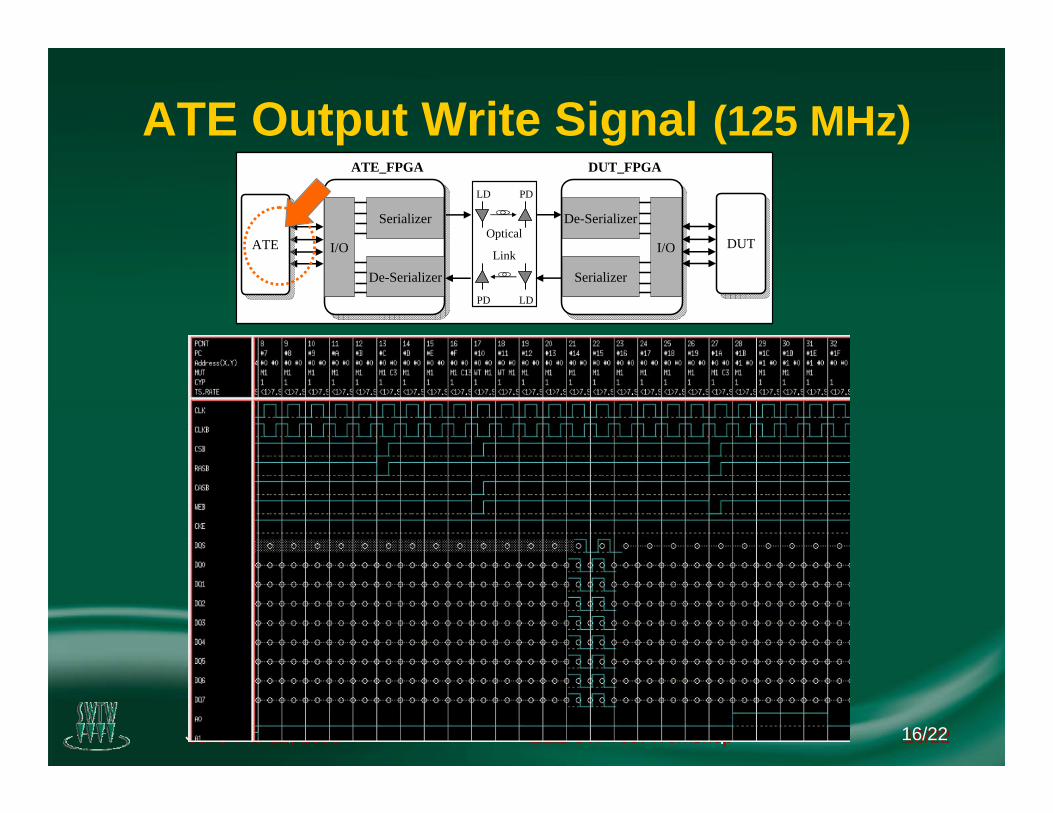
ATE Output Write Signal (125 MHz)

June 7 to 10, 2009June 7 to 10, 2009 IEEE SW Test WorkshopIEEE SW Test Workshop 17/2217/22
DUTDUT
ATE_FPGA
I/OOptical
Link
DUT_FPGA
De-Serializer
Serializer
I/OATEATE
PD LD
LD PD
De-Serializer
Serializer
DUTDUT
ATE_FPGA
I/OOptical
Link
DUT_FPGA
De-Serializer
Serializer
I/OATEATE
PD LD
LD PD
De-Serializer
Serializer
Input Signal into FPGA_ATE (125 MHz)
ActiveWrite
WriteOut
Pre-charge
ActiveWrite
WriteOut
Pre-charge
- The same logic compared with ATE function logic

June 7 to 10, 2009June 7 to 10, 2009 IEEE SW Test WorkshopIEEE SW Test Workshop 18/2218/22
DUTDUT
ATE_FPGA
I/OOptical
Link
DUT_FPGA
De-Serializer
Serializer
I/OATEATE
PD LD
LD PD
De-Serializer
Serializer
DUTDUT
ATE_FPGA
I/OOptical
Link
DUT_FPGA
De-Serializer
Serializer
I/OATEATE
PD LD
LD PD
De-Serializer
Serializer
Received Serialized Signal (2.5 Gbps)
• Amplitude = 270 mV • Jitter = 54 ps • tR/tF = 180 ps/164 ps
2.5 Gbps
Using Oscilloscope

June 7 to 10, 2009June 7 to 10, 2009 IEEE SW Test WorkshopIEEE SW Test Workshop 19/2219/22
DUT Input Signal at FPGA_DUT (125 MHz)
DUTDUT
ATE_FPGA
I/OOptical
Link
DUT_FPGA
De-Serializer
Serializer
I/OATEATE
PD LD
LD PD
De-Serializer
Serializer
DUTDUT
ATE_FPGA
I/OOptical
Link
DUT_FPGA
De-Serializer
Serializer
I/OATEATE
PD LD
LD PD
De-Serializer
Serializer
CLK vs. CAS CLK vs. CAS (skew-free)
DQS vs. DQ_7 DQS vs. DQ_7 (skew-free)
[ Skew Control using FPGA IO-delay ]
CLK = 2 ns Delay DQS = 2 ns Delay

June 7 to 10, 2009June 7 to 10, 2009 IEEE SW Test WorkshopIEEE SW Test Workshop 20/2220/22
DUTDUT
ATE_FPGA
I/OOptical
Link
DUT_FPGA
De-Serializer
Serializer
I/OATEATE
PD LD
LD PD
De-Serializer
Serializer
DUTDUT
ATE_FPGA
I/OOptical
Link
DUT_FPGA
De-Serializer
Serializer
I/OATEATE
PD LD
LD PD
De-Serializer
Serializer
Read Signal into ATE Comparator
All good read signal with synchronous operation in front of ATE.

June 7 to 10, 2009June 7 to 10, 2009 IEEE SW Test WorkshopIEEE SW Test Workshop 21/2221/22
Hardware Performance
4 times expansion
1/40 reduction
1/8 reduction
Advantage
by Optical SplitterNot expandedATE channel
expansion
2 ea(Parallel
modules used)
80 ea(only write-mode)
# of Optical Module (TX and RX)
5 ch40 ch# of Optical fiber
for 1 DUT
Optical SerDesSystem
Conventional System
TypePerformance

June 7 to 10, 2009June 7 to 10, 2009 IEEE SW Test WorkshopIEEE SW Test Workshop 22/2222/22
Summary• Optical signal 4 times splitting scheme and SerDes
techniques for a multi-parallel high speed memory test • An actual write/read optical memory test operation
• Optical fiber channels of 87 % and Optical module of 95 % are reduced dramatically, compared to a conventional optical interface
• Further, this scheme, with proper modifications and optimizations in terms of size and power, might be applied for CPU-memory optical interconnects in the future computing environment.