optical network-on-chip architectures and designs
TRANSCRIPT

UNLV Theses, Dissertations, Professional Papers, and Capstones
5-2011
Optical network-on-chip architectures and designs Optical network-on-chip architectures and designs
Lei Zhang University of Nevada, Las Vegas
Follow this and additional works at: https://digitalscholarship.unlv.edu/thesesdissertations
Part of the Computer and Systems Architecture Commons, Digital Communications and Networking
Commons, and the Hardware Systems Commons
Repository Citation Repository Citation Zhang, Lei, "Optical network-on-chip architectures and designs" (2011). UNLV Theses, Dissertations, Professional Papers, and Capstones. 1037. http://dx.doi.org/10.34917/2410819
This Dissertation is protected by copyright and/or related rights. It has been brought to you by Digital Scholarship@UNLV with permission from the rights-holder(s). You are free to use this Dissertation in any way that is permitted by the copyright and related rights legislation that applies to your use. For other uses you need to obtain permission from the rights-holder(s) directly, unless additional rights are indicated by a Creative Commons license in the record and/or on the work itself. This Dissertation has been accepted for inclusion in UNLV Theses, Dissertations, Professional Papers, and Capstones by an authorized administrator of Digital Scholarship@UNLV. For more information, please contact [email protected].

OPTICAL NETWORK-ON-CHIP
ARCHITECTURES AND
DESIGNS
by
Lei Zhang
Bachelor of Science
Yanshan University, China
1997
Master of Science
Tianjin University, China
2004
A dissertation submitted in partial fulfillment of
the requirements for the
Doctor of Philosophy in Electrical Engineering
Department of Electrical and Computer Engineering
Howard R. Hughes College of Engineering
Graduate College
University of Nevada, Las Vegas
May 2011

Copyright by Lei Zhang 2011
All Rights Reserved

iii
THE GRADUATE COLLEGE
We recommend the dissertation prepared under our supervision by
Lei Zhang
entitled
Optical Network-on-Chip Architectures and Designs
be accepted in partial fulfillment of the requirements for the degree of
Doctor of Philosophy in Electrical Engineering Department of Electrical and Computer Engineering
Emma E. Regentova, Committee Chair
Venkatesan Muthukumar, Committee Member
Yingtao Jiang, Committee Member
Ajoy K. Datta, Graduate Faculty Representative
Ronald Smith, Ph. D., Vice President for Research and Graduate Studies
and Dean of the Graduate College
May 2011

iv
ABSTRCT
Optical Network-on-Chip
Architectures and
Designs
by
Lei Zhang
Dr. Emma E. Regentova, Examination Committee Chair
Associate Professor of Electrical and Computer Engineering
University of Nevada, Las Vegas
As indicated in the latest version of ITRS roadmap, optical wiring is a viable
interconnection technology for future SoC/SiC/SiP designs that can provide broad band
data transfer rates unmatchable by the existing metal/low-k dielectric interconnects. In
this dissertation study, a set of different optical interconnection architectures are
presented for future on-chip optical micro-networks.
Three Optical Network-on-Chip (ONoC) architectures, i.e., Wavelength Routing
Optical Network-on-Chip (WRON), Redundant Wavelength Routed Optical Network
(RDWRON) and Recursive Wavelength Routed Optical Network (RCWRON) are
proposed. They are fully connected networks designed based on passive switching
Microring Resonator (MRR) optical switches. Given enough different routing optical
wavelengths, between any two nodes in the system a bi-directional communication
channel can be built. WRON, RDWRON and RCWRON share the similar network
structure with different specialties that fit to different applications.
A new topology of packet switching NoC architecture, i.e., Quartered Recursive
Diagonal Torus (QRDT) is proposed. It is designed by overlaying diagonal torus. Due to
its small diameter and rich routing recourses, QRDT leads to highly scalable NoCs.

v
By combining WRON‟s interconnection property and QRDT‟s network topology, a
group of 2D-Torus based Packet Switching ONoC (TON) architectures is proposed. The
TON is further refined to a generalized open-topology ONoC architecture, called
Generalized 2D-Torus-based Optical Network-on-Chip (GTON). The communication
protocol in TON is packet switching. The advantages of GTON stem from Wavelength
Division Multiplexing (WDM), Direct Optical Channel (DOC) and MRR passive
switching. As result, GTON architecture is highly scalable, has an ultra-high bandwidth,
consumes a low power, and supports fault-tolerant routing. The work includes other
issues such as channel design, analyses of the transmission power loss and the buffer.

vi
TABLE OF CONTENTS
ABSTRCT.......................................................................................................................... iii
TABLE OF CONTENTS ................................................................................................... vi
LIST OF TABLES .............................................................................................................. x
LIST OF FIGURES .......................................................................................................... xii
CHAPTER 1 INTRODUCTION ....................................................................................... 1
CHAPTER 2 OPTICAL NETWORK-ON-CHIP OVERVIEW ........................................ 9
2.1 Optical Interconnection Components ....................................................................... 9
2.1.1 On-Chip Lasers .................................................................................................. 9
2.1.1.1 Raman Laser ................................................................................................ 9
2.1.1.2 Vertical Cavity Surface Emitting Lasers (VCSEL) ................................... 10
2.1.1.3 Mode-Lock Evanescent Lasers (MLLs) .....................................................11
2.1.1.4 Ge-on-Si Laser ........................................................................................... 12
2.1.2 Optical Modulators ........................................................................................... 13
2.1.2.1 Mach-Zehnder Modulator (MZM) ............................................................ 13
2.1.2.2 Cascaded Silicon Micro-ring Modulator ................................................... 14
2.1.3 Photodetectors .................................................................................................. 15
2.1.3.1 PIN Photodetector...................................................................................... 15
2.1.3.2 Germanium Avalanche Photodetector ....................................................... 16
2.1.4 Micro Ring Resonator (MRR) Optical Switch ................................................. 17
2.2 Current Works on ONoC Architectures .................................................................. 21
CHAPTER 3 WAVELENGTH ROUTED OPTICAL NETWORK-ON-CHIP
ARCHITECTURES .......................................................................................................... 25
3.1 Basic Structures of WRON ..................................................................................... 25
3.1.1 WRON Type I .................................................................................................. 25
3.1.2 WRON Type II ................................................................................................. 28
3.2 Routing Scheme of WRON and Its System Organization ...................................... 31
3.3 System Organization ............................................................................................... 34
3.4 Conclusion .............................................................................................................. 35
CHAPTER 4 2-D REDUNDANT OPTICAL NETWORK-ON-CHIP
ARCHITECTURES .......................................................................................................... 36
4.1 Basic Units in RDWRON ....................................................................................... 36
4.1.1 Inverse Connector (IC) ..................................................................................... 36
4.1.2 Construction of 2-D Redundant Optical Network............................................ 37
4.2 Features of 2-D RDWRON ..................................................................................... 38

vii
4.3 The routing scheme of N2-RDWRON .................................................................... 39
4.3.1 Level1 RDWRON routing scheme .................................................................. 39
4.3.2 Level2 RDWRON routing scheme .................................................................. 40
4.4 Conclusion .............................................................................................................. 42
CHAPTER 5 2-D RECURSIVE OPTICAL NETWORK-ON-CHIP ARCHITECTURES
........................................................................................................................................... 43
5.1 Structure of 2-D Recursive Optical Network.......................................................... 43
5.1.1 Construction of 2-D RCWRON ....................................................................... 43
5.1.2 Fault Tolerance Capability ............................................................................... 45
5.2 Routing Scheme of 2-D RCWRON ........................................................................ 45
5.2.1 Routing Wavelength Assignment ..................................................................... 45
5.2.2 Routing Scheme for RCWRON ....................................................................... 47
5.2.3 One Routing Example ...................................................................................... 51
5.3 Conclusion .............................................................................................................. 53
CHAPTER 6 QUARTERED RECURSIVE DIAGNAL TORUS NETWORK-ON-CHIP
ARCHITECTURES .......................................................................................................... 55
6.1 Introduction ............................................................................................................. 55
6.2 QRDT Structure and Its Network Properties .......................................................... 57
6.3 Johnson Codes and Functions to Manipulate the Codes ......................................... 60
6.3.1 Johnson Codes .................................................................................................. 60
6.3.2 Basic Functions of Johnson Codes ................................................................... 61
6.4 Routing Algorithm for QDRT ................................................................................. 62
6.4.1 JCVR Algorithm ............................................................................................... 62
6.4.2 Fault Tolerance Routing for QRDT under Single Link/Node Failure .............. 64
6.5 Conclusion .............................................................................................................. 67
CHAPTER 7 PACKET SWITCHING OPTICAL NETWORK-ON-CHIP
ARCHITECTRUES .......................................................................................................... 69
7.1 Introduction ............................................................................................................. 69
7.2 TON Architectures .................................................................................................. 70
7.2.1 Interconnections in TON network .................................................................... 70
7.2.2 Optical Interconnection Unit (OIU) ................................................................. 71
7.2.3 Optical-Electrical Router (OER) ...................................................................... 71
7.2.4 Directed Optical Channel (DOC) ..................................................................... 72
7.3 TON-I Architecture ................................................................................................. 73
7.3.1 TON-I Topology ............................................................................................... 73
7.3.2 Channel Realization ......................................................................................... 74
7.3.3 Routing Table of OIUs in TON-I ..................................................................... 76
7.3.4 OIUs in TON-I ................................................................................................. 76
7.3.5 OERs in TON-I ................................................................................................ 76
7.4 TON-II Architecture ................................................................................................ 77
7.4.1 TON-II Topology ............................................................................................. 77
7.4.2 Channel Realization ......................................................................................... 78
7.4.3 Routing Table of OIUs in TON-II .................................................................... 79

viii
7.4.4 OIUs in TON-II ................................................................................................ 80
7.4.5 OERs in TON-II ............................................................................................... 81
7.5 TON-III Architecture .............................................................................................. 82
7.5.1 TON-III Topology ............................................................................................ 82
7.5.2 Channel Realization ......................................................................................... 83
7.5.3 Routing Table of OIUs in TON-III ................................................................... 85
7.5.4 OIUs in TON-III ............................................................................................... 86
7.5.5 OER in TON-III ............................................................................................... 86
7.6 TON Architecture Properties .................................................................................. 88
7.6.1 Topological Properties of TON ........................................................................ 88
7.6.2 Architecture Properties of TON ....................................................................... 89
7.7 Routing Algorithms of TON Architectures ............................................................. 90
7.7.1 Johnson Code Addressing for TON.................................................................. 90
7.7.1.1 Addressing Nodes in TON ......................................................................... 90
7.7.1.2 Nodes Coordinates and Address Association ............................................ 90
7.7.2 Routing Functions in TON ............................................................................... 91
7.7.2.1 Routing Direction Function fr .................................................................... 91
7.7.2.2 Routing Address Function fd ...................................................................... 92
7.7.2.3 Routing channel function fI, fII and fIII ....................................................... 93
7.7.2.4 Routing vector function fv1, fv2 and fv3 ....................................................... 96
7.7.3 Relationship between Nodes Coordinates and Address ................................... 99
7.7.4 Deterministic Routing Algorithm for TONs .................................................. 100
7.7.4.1 Dynamic routing ...................................................................................... 100
7.7.4.2 Predetermined routing ............................................................................. 103
7.7.5 Basic Adaptive Routing Algorithm for TONs ................................................ 105
7.7.5.1 Adaptive dynamic routing ....................................................................... 106
7.7.5.2 Adaptive predetermined routing .............................................................. 108
7.8 Simulation and Analysis ........................................................................................110
7.8.1 Simulation Setup .............................................................................................110
7.8.2 Simulation Results for TON-I ......................................................................... 111
7.8.3 Simulation Results for TON-II ........................................................................113
7.8.4 Simulation Results for TON-III ......................................................................115
7.9 Power Analysis.......................................................................................................117
7.9.1 Electrical Back-end Components ....................................................................117
7.9.2 Transmission Power Loss ................................................................................118
7.10 Conclusion ............................................................................................................ 121
CHAPTER 8 GENERALIZED PACKET SWITCHING OPTICAL NETWORK-ON-
CHIP ARCHITECTURES .............................................................................................. 122
8.1 Introduction ........................................................................................................... 122
8.2 GTON Architecture Overview .............................................................................. 123
8.3 GTON Design Schema ......................................................................................... 125
8.3.1 GTON-XII Topology ...................................................................................... 126
8.3.2 Network Properties of GTON-XII ................................................................. 127
8.3.3 Channel Mapping in GTON-XII .................................................................... 128
8.3.4 Routing Wavelength Assignment ................................................................... 136

ix
8.3.5 OIU Design .................................................................................................... 139
8.3.6 OER Design.................................................................................................... 142
8.3.7 Architecture Properties of GTON-XII ........................................................... 146
8.4 Routing Algorithm of GTON-XII ......................................................................... 147
8.4.1 Johnson Code Addressing for GTON-XII ...................................................... 147
8.4.1.1 Addressing Nodes in GTON-XII ............................................................. 147
8.4.1.2 Nodes Coordinates and Address Association .......................................... 147
8.4.2 Routing functions for GTON-XII .................................................................. 148
8.4.2.1 Routing Direction Function fr .................................................................. 148
8.4.2.2 Routing Address Function fd .................................................................... 148
8.4.2.3 Routing channel vector V ........................................................................ 148
8.4.2.4 Channel combination transforms in GTON-XII ...................................... 149
8.4.3 Deterministic Routing Algorithm for GTON-XII .......................................... 150
8.4.4 Adaptive Routing Algorithm for GTON-XII ................................................. 151
8.4.5 Fault Tolerant Routing Algorithm for GTON-XII ......................................... 152
8.5 Simulation and Analysis ....................................................................................... 154
8.5.1 Simulation Setup ............................................................................................ 154
8.5.2 Simulation Results.......................................................................................... 155
8.6 Network Properties of GTON Architectures ......................................................... 157
8.6.1 Buffer Analysis ............................................................................................... 157
8.6.2 Analysis of Channel Availability .................................................................... 158
8.6.3 Maximum DOC Length ................................................................................. 159
8.6.4 Topological Diversity of GTON..................................................................... 159
8.6.5 Transmission Power Loss ............................................................................... 160
8.7 Conclusion ............................................................................................................ 161
CHAPTER 9 CONCLUSION........................................................................................ 163
APPENDIX A PROOF OF PROPOSITIONS 1-3 .......................................................... 165
APPENDIX B PROOF OF PROPOSITIONS 4-6 ......................................................... 174
APPENDIX C PROOF OF LEMMA 7 AND LEMMA 8 .............................................. 180
REFERENCES ............................................................................................................... 185
VITA ............................................................................................................................... 195

x
LIST OF TABLES
Table 1 The wavelength assignment of 4-WRON. .................................................... 31
Table 2 The wavelength assignment of 5-WRON. .................................................... 32
Table 3 The routing wavelengths assignment of 32-RCWRON. ............................... 40
Table 4 Routing wavelengths for Level1 42-RDWRON. ........................................... 53
Table 5 Routing wavelengths for Level2 42-RDWRON. ........................................... 53
Table 6 Routing wavelengths of 42×4
2RCWRON ..................................................... 53
Table 7 Different networks‟ diameter (R) and average distance (AD) ....................... 60
Table 8 Channel Realization in TON-I ....................................................................... 74
Table 9 Routing truth table of OIUs in TON-I ........................................................... 76
Table 10 Channel Realization for I-Node in TON-II ................................................... 79
Table 11 Channel Realization for II-Node in TON-II .................................................. 79
Table 12 Routing truth table of I-OIU in TON-II......................................................... 80
Table 13 Routing truth table of II-OIU in TON-II ....................................................... 80
Table 14 Routing paths in TON-III .............................................................................. 84
Table 15 Routing paths in TON-III .............................................................................. 85
Table 16 Routing truth table for I-OIU of TON-II ....................................................... 85
Table 17 Routing truth table for II-OIU of TON-II ...................................................... 86
Table 18 Topology Properties....................................................................................... 89
Table 19 Architecture Properties of TON-1 ................................................................. 90
Table 20 Simulation Setting ........................................................................................110
Table 21 Estimated energy of optical components ......................................................118
Table 22 Estimated energy consumption of single channel in TON-I, II, and III .......118
Table 23 Estimated energy consumption of single channel in TON-I, II and III ........118
Table 24 Optical Power Budget ..................................................................................119
Table 25 Transmission Power Loss in TON-I .............................................................119
Table 26 Transmission Power Loss in TON-II ............................................................119
Table 27 Transmission Power Loss in TON-III ......................................................... 120
Table 28 Diameter (D) and Average Distance (AD) for Different Networks. ........... 128
Table 29 I-Node Level1 Chanel Mapping in GTON-XII ........................................... 129
Table 30 I-Node Level2 Chanel Mapping in GTON-XII ........................................... 129
Table 31 I-Node Level3 Chanel Mapping in GTON-XII ........................................... 130
Table 32 II-Node Level1 Chanel Mapping in GTON-XII ......................................... 130
Table 33 II-Node Level2 Chanel Mapping in GTON-XII ......................................... 130
Table 34 II-Node Level3 Chanel Mapping in GTON-XII ......................................... 131
Table 35 Routing Table for I-Nodes ........................................................................... 137
Table 36 Routing Table for II-Nodes ......................................................................... 137
Table 37 Remapped Routing Table for I-Nodes and II-Nodes ................................... 138
Table 38 Routing Table for OIU in GTON-XII .......................................................... 139
Table 39 Routing Table for OIU in GTON-XII .......................................................... 139
Table 40 Routing Table of Wavelength w1 in I-OIU .................................................. 140
Table 41 Routing Table of Wavelength w2 in I-OIU .................................................. 140
Table 42 Architecture Properties of GTON-XII ......................................................... 147
Table 43 Simulation Setting ....................................................................................... 155
Table 44 Optical Power Budget ................................................................................. 160

xi
Table 45 Transmission Power Loss in DOCs ............................................................. 160

xii
LIST OF FIGURES
Figure 1 Imaginary illustration of future ONoC chip .................................................... 3
Figure 2 Conceptual 3DI of future ONoC ICs ............................................................... 3
Figure 3 Wavelength Devision Multiplexing (WDM) ................................................... 7
Figure 4 Schematic of Raman laser ............................................................................. 10
Figure 5 Schematic of the vertical cavity surface emitting laser ..................................11
Figure 6 Schematic of the mode locked silicon evanescent laser. ............................... 12
Figure 7 Germanium-on-silicon laser schematics ....................................................... 13
Figure 8 MZM optical modulator ................................................................................ 14
Figure 9 Schematics of a WDM optical interconnection system ................................. 15
Figure 10 Cross section of a PIN PD with DNW in an epi-CMOS process .................. 16
Figure 11 Schematic of Germanium avalanche photodetector ...................................... 17
Figure 12 MRR based optical switch. ............................................................................ 19
Figure 13 Basic functions of the optical switch. ............................................................ 20
Figure 14 MRR optical switch functions ....................................................................... 21
Figure 15 Type I WRON. ............................................................................................... 26
Figure 16 Type II WRON .............................................................................................. 30
Figure 17 System organization of a 4-WRON. .............................................................. 35
Figure 18 Structure of an N-IC ...................................................................................... 37
Figure 19 Structure of N2-RDWRON. ........................................................................... 37
Figure 20 Examples of N2-RDWRON. .......................................................................... 38
Figure 21 Structure of N2-RCWRON. ........................................................................... 44
Figure 22 Structures of 42-RDWRON. .......................................................................... 51
Figure 23 Structures of 42-RCWRON. .......................................................................... 52
Figure 24 Structure of 4-QRDT. .................................................................................... 58
Figure 25 Channeling in QRDT ..................................................................................... 59
Figure 26 Vector routing algorithm for QRDT. ............................................................. 63
Figure 27 Two cases under single link fault. ................................................................. 66
Figure 28 Two cases under single node fault ................................................................. 67
Figure 29 Structure of 6×6 Torus-based Optical Network-on-chip ............................... 70
Figure 30 Structure of 8×8 TON and DOC examples. .................................................. 73
Figure 31 TON-I network topology ............................................................................... 74
Figure 32 OIU structure of TON-I ................................................................................. 76
Figure 33 OER unit in TON-I ........................................................................................ 77
Figure 34 TON-II network topology. ............................................................................. 78
Figure 35 OIU in TON-II ............................................................................................... 80
Figure 36 OERs in TON-II ............................................................................................ 82
Figure 37 TON-III network topology ............................................................................ 83
Figure 38 OIU in TON-III ............................................................................................. 86
Figure 39 OERs in TON-III ........................................................................................... 88
Figure 40 Algorithm to update {m}. .............................................................................. 96
Figure 41 Algorithm to generate the routing vector V for TON-I. ................................ 97
Figure 42 Algorithm to generate the routing vector V for TON-II. ............................... 98
Figure 43 Algorithm to generate the routing vector V for TON-III. .............................. 99
Figure 44 Dynamic routing algorithm of I-TON. ........................................................ 101

xiii
Figure 45 Dynamic routing algorithm of II-TON. ....................................................... 102
Figure 46 Dynamic routing algorithm of III-TON. ..................................................... 103
Figure 47 Predetermined routing algorithm of I-TON. ............................................... 104
Figure 48 Predetermined routing algorithm of II-TON. .............................................. 105
Figure 49 Predetermined routing algorithm of III-TON. ............................................. 105
Figure 50 Adaptive dynamic routing algorithm of I-TON. ......................................... 107
Figure 51 Adaptive dynamic routing algorithm of II-TON. ........................................ 107
Figure 52 Adaptive dynamic routing algorithm of III-TON. ....................................... 108
Figure 53 Adaptive dynamic routing algorithm of I-TON. ......................................... 108
Figure 54 Adaptive dynamic routing algorithm of II-TON. ........................................ 109
Figure 55 Adaptive dynamic routing algorithm of III-TON. ....................................... 109
Figure 56 Average frame transmission time in TON-I ................................................. 111
Figure 57 Average input buffer utilization in TON-I ....................................................112
Figure 58 Maximum input buffer utilization in TON-I ................................................112
Figure 59 Average frame transmission time in TON-II ................................................113
Figure 60 Average input buffer utilization in TON-II ..................................................114
Figure 61 Maximum input buffer utilization in TON-II ...............................................114
Figure 62 Average frame transmission time in TON-III ...............................................115
Figure 63 Average input buffer utilization in TON-III .................................................116
Figure 64 Maximum input buffer utilization in TON-III ..............................................116
Figure 65 6×6 GTON network topology ..................................................................... 123
Figure 66 A 6×6 GTON architecture and examples of DOCs. .................................... 124
Figure 67 Node channel map in GTON-XII ................................................................ 127
Figure 68 Mapping I-Node Level 1 channels in 6×6 GTON-XII ................................ 131
Figure 69 Mapping I-Node Level2 channels in 6×6 GTON-XII ................................. 132
Figure 70 Mapping I-Node Level3 channels in 6×6 GTON-XII ................................. 133
Figure 71 Mapping II-Node Level1 channels in 6×6 GTON-XII................................ 134
Figure 72 Mapping of II-Nodes Level 2 channels in 6×6 GTON-XII ......................... 135
Figure 73 Mapping II-Node Level 3 channels in 6×6 GTON-XII............................... 136
Figure 74 Integrating single wavelength switches into OIU ....................................... 141
Figure 75 Optical switch and cross-bridge. ................................................................. 142
Figure 76 I-OIU and II-OIU in GTON-XII ................................................................. 142
Figure 77 Routing wavelength assignment in GTON-XII ........................................... 144
Figure 78 I-OER and II-OER structures in GTON-XII ............................................... 146
Figure 79 Deterministic routing algorithm for GTON-XII. ......................................... 151
Figure 80 Adaptive routing algorithm for GTON-XII. ................................................ 152
Figure 81 Direct fault tolerant routing algorithm for GTON-XII. ............................... 154
Figure 82 Average packet transmission time in GTON-XII ........................................ 156
Figure 83 Average input buffer utilization in GTON-XII ............................................ 156
Figure 84 Maximum input buffer utilization in GTON-XII ........................................ 157
Figure 85 Channel utilization in GTON-XII ............................................................... 158
Figure 86 Structure of the Tri-network for a 4×4 WRON. .......................................... 167
Figure 87 Structure of 8-WRON. ................................................................................ 175
Figure 88 Two type of connections between IC and WRON. ..................................... 176
Figure 89 Straight connection block. ........................................................................... 177
Figure 90 Transform N2-RDWRON to N-WRON. ...................................................... 178

xiv
Figure 91 Structure of 3-QSN. ..................................................................................... 180
Figure 92 Partition of QRDT to QSNs. ....................................................................... 182

1
CHAPTER 1
INTRODUCTION
Transistor integration is a technology trend. It is estimated that by 2015, 100 billion
transistors can be integrated on a 300 mm2 die [1]. This enables a large number of
processing/IP cores integration into a multiprocessor system-on-chip (MPSoC) or chip
multiprocessor (CMP) design. The International Technology Roadmap for
Semiconductors (ITRS) has projected a Tera-scale computing 3D SiP by 2015, in which
the target number of cores integrated on a chip is 1,000 [1]. The interconnection and
associated communication infrastructures play a central role for the performance of
MPSoCs [2]. For MPSoCs, a vital challenge is to realize a scalable on-chip
communication infrastructure that meets the large bandwidth capacities and stringent
latency in a power-efficient fashion [3]. Networks-on-Chip (NoC) can improve the on-
chip communication bandwidth of MPSoCs and has been widely adopted as an
alternative to the traditional bus-based on-chip communication. However, with the
continuously shrinking size of features and increasing complexity of NoCs, traditional
metallic interconnected NoCs cannot satisfy the bandwidth and latency requirements
within the on-chip power budget due to its limited bandwidth, long delay, and relatively
high power consumption [4].
Two important issues come out. 1) Material and signal front: optics (optical signal) to
replace metal (electrical signal) based interconnection (signal). Looking further into the
future, optical wiring could significantly raise the performance limits hindered by
metal/dielectric interconnects [5]. Optical fibers are capable of carrying encoded optical
data in terabits per second while maintaining near speed-of-light limited transit latencies

2
[6]. Moreover, the power consumed by optical interconnect is almost independent of the
interconnect length [7], and is much less compared with electrical interconnect (around
1/10 in general) [8]. 2) Architecture front: it is inevitable that Network on Chip (NoC)
will replace the traditional SoC architecture. A NoC system is composed of a large
number of processing units communicating to other units through an interconnection
network. This interconnection network plays an important role in achieving high
performance, scalability, power efficiency, and fault tolerance.
These two issues when combined lead to Optical Network on Chip (ONoC) (Figure 1
[9]). With the potential of delivering performance-per-watt scaling, ONoC has been
considered as a promising candidate to overcome the limitations of electronic NoCs,
which enables high bandwidth and low contention routing of data [6] using Wavelength
Division Multiplexing (WDM)-enabled optical waveguides [10]. Here optical switch [11]
and waveguides [12] are used in ONoC to realize the same function as a conventional
electrical router but with routing based on wavelength and with no need for an arbiter
[13].
Basically optical interconnection can bring the following advantages:
Ultra-high bandwidth (Tera-scale);
Extremely low energy consumption/transmission latency;
Negligible electromagnetic interference (EMI);
Unlimited chip size.

3
Figure 1 Imaginary illustration of future ONoC chip [9]
For example, optical data routing in a 64 cores chip could have 40 times the power
efficiency of the traditional wire connections in estimation [14].
Conceptual 3D Integration [15, 16] (3DI) of future ONoC CMOS ICs is shown in
Figure 2 [5, 17].
Figure 2 Conceptual 3DI of future ONoC ICs [17]

4
The main advantage of optical interconnection relies on the bit-rate-transparent
property of photonic medium [18]. This property facilitates the transmission of a very
high bandwidth in optical networks while avoiding the high power cost typically
associated with them in traditional electronic networks [19]. At a chip-scale, the power
dissipated on a photonic link is independent of transmission distance because of the ultra-
low loss in optical waveguides. Energy dissipation remains essentially the same whether
a message travels between two cores that are 2mm or 2cm apart [20]. Furthermore,
multiple optical signals of different wavelengths can be transmitted within the same
waveguide without confliction with wavelength-division multiplexing (WDM)
technology [21, 22] (Figure 3), and that can extremely increase the optical
communication bandwidth.
The dissertation study presented in this paper targets to the architecture of optical
interconnected network-on-chip architectures. A set of different interconnect architectures
are proposed for future on-chip optical micro-networks.
The first Optical Network-on-Chip (ONoC) architecture proposed is the Wavelength
Routing Optical Network-on-Chip which is referred as WRON. Both its construction
scheme and routing algorithm are generalized. WRON is a fully connected network.
Given enough different routing optical wavelengths, between any two nodes in the
system a bi-directional communication channel can be built. And all these channels are
non-conflicting to each other.
With WRON as the primitive platform, a new redundant architecture referred as the
Redundant Wavelength Routed Optical Network (RDWRON). The routing algorithm of
RDWRON is generalized and presented. RDWRON is also a fully connected network too.
5
Given enough different routing optical wavelengths, between any two nodes in the
system multiple bi-directional communication channels can be built. And all these
channels, each between two nodes or among any pairs of nodes are all non-conflicting to
each other. This property can be applied to build micro-networks to interconnect
multicore clusters.
Based on RDWRON architecture, a new recursive architecture is proposed which is
referred as the Recursive Wavelength Routed Optical Network (RCWRON). The routing
algorithm of RDWRON is generalized and presented. RCWRON is a fully connected
network as well. As recursive architecture RCWRON possesses better scalability and
fault isolating capability.
WRON, RDWRON and RCWRON are all fully connected networks. Each different
pair of two nodes in the network communicates via light in a different optical wavelength.
And obvious the total number of different wavelength can be integrated on a single chip
is very restricted, normally no higher than the level of 10s. Hence the scalability of fully
connected ONoC structures is limited, which means such kind of architectures cannot be
applied to manycore systems.
On the other side, a new NoC architecture is propose, referred as the Quartered
Recursive Diagonal Torus (QRDT), which is constructed by overlaying diagonal torus.
Due to its small diameter and rich routing recourses, QRDT is determined to be well
suitable to construct highly scalable NoCs. In QRDT, data packets can be routed through
a proposed minimal routing algorithm based on the Johnson codes that have traditionally
been used in finite state machine designs. It has been shown that this proposed routing
algorithm with minor modifications is capable of handling the single link/node failure.

6
To solve the limitation of fully connected ONoC architecture, a new group of ONoC
architectures is proposed, based on the combination of WRON and QRDT by which the
former one is adopted as the optical interconnection device and the later one‟s network
topology is applied. The first is a family referred as 2D-Torus based Packet Switching
ONoC, or TON architectures. As it is named, data communication in TON is
implemented via packet switching. By employing a limited number of different routing
wavelengths in Wavelength Division Multiplexing (WDM), each node in the TON
network has the same number of optical channels. Then the communication between a
pair of remote nodes can be achieved by relaying data packets among different optical
channels of intermediary nodes between this pair of remote nodes. Moreover, a new
concept called Directed Optical Channel (DOC) is introduced on the first time in TON
architecture. The DOC is a realization of the channel with a light path between two nodes
that consists of one or more physical links and optical interconnection units. By utilizing
a predetermined routing wavelength and with properly designed optical interconnection
units light can travel through the DOC without any relay or arbitration. DOCs can be
built between any two nodes. Packet Switching, WDM and DOC, this combination
enables the TON architecture unlimited scalability, ultra-high bandwidth, low power
consumption (compare with optical tuning architectures) and practical feasibility. And the
transmission latency is also maintained in an acceptable level.
Totally three different TON architectures are presented, denoted as TON-I, TON-II
and TON-III, with 4, 8 and 10 different DOCs in each node in the network architecture,
respectively. And the routing algorithms for each architecture are addressed in detail, with
the network performance evaluation presented with simulation results.

7
The topologies of TON architectures are fixed. But for different purposes networks in
different topologies may be required. From this view, an improved version of TON
architecture is proposed, denoted as Generalized 2D-Torus-based Optical Network-on-
Chip (GTON), which is a generalized packet switching optical NoC. Given sufficient
routing wavelengths, any network topology can be implemented in GTON. A systematic
approach of the design of network interconnections and routers is presented in detail. The
use of passive MRR switching, Wavelength Division Multiplexing (WDM) and Direct
Optical Channels (DOC) allows for attaining high bandwidth and makes GTON fault
tolerant. The number of different routing wavelengths required in GTON architecture is
limited. Simulation results presented has shown the performance of the architecture.
Related issues such as channel design, transmission power loss and the buffer analysis of
GTON are also provided explicitly.
Figure 3 Wavelength Devision Multiplexing (WDM) [22]
The dissertation is organized as follows. 0 introduces the concepts of ONoC and
Integrated Transmitter Die
Integrated Receiver Die

8
contributions of the dissertation study. Chapter 2 presents a survey of latest
breakthroughs in developing on-chip optical components/devices, and a summary of most
ONoC architectures proposed so far. From 0 to 0, three different fully connected ONoC
architectures WRON, RDWRON and RCWRON are presented explicitly with their
routing algorithms generalized in detail. 0 presents an improved network topology QRDT
which is the foundation of the later work. Based on the QRDT architecture, the packet
switching ONoC architect family TON is presented in 0 with three typical cases TON-I,
II and III. And their routing algorithms and related network properties are also addressed
in this chapter. Furthermore, in 0 the TON architecture is refined and a generalized open-
topology packet switching ONoC architecture GTON is presented with detail design
scheme. And routing algorithm plus network properties analyses are presented in this
chapter. Finally Chapter 9 concluded the dissertation study with the schedule of future
exploration.

9
CHAPTER 2
OPTICAL NETWORK-ON-CHIP OVERVIEW
2.1 Optical Interconnection Components
In the past several years, the field of silicon photonics attracts attention of industrial
and academic research groups [23]. A great number of essential silicon photonic
components have been created such as on-chip laser sources, optical modulators[24, 25],
waveguides [26] and photodetectors. Intel has announced a Tera-scale laser modulator in
2007 [24]. The first Ge-on-Si laser has been invented by MIT in March 2010 [27], while
IBM invented a germanium avalanche photodetector used on-chip around the same time
[28, 29]. These demonstrated silicon photonic devices and technologies make optical
network-on-chip (ONoC) viable.
2.1.1 On-Chip Lasers
2.1.1.1 Raman Laser
A major attraction of Raman lasers is their ability to use light from an optical “pump”
to generate coherent light emission in wavelength regions that are hard to reach with
other conventional types of lasers. In addition, Raman lasers can be made from materials
such as silicon that do not possess suitable energy band structures to produce laser light
by stimulated emission.
The silicon Raman laser was constructed from a low loss silicon-on-insulator (SOl)
rib waveguide in a ring cavity configuration, as shown in Figure 4 [22, 30]. The
racetrack-shaped ring laser cavity was connected to a straight bus waveguide by means of
a directional coupler that couples both pump and Raman lasing signals into and out of the
cavity. The pump coupled into the laser cavity generates optical gain by stimulated

10
Raman scattering inside the silicon waveguide at the first-order Stokes wavelength,
which is 15.6 THz redshifted from the pump. The gain increases with pump power, and
the lasing threshold is reached when the gain equals the total cavity loss. The first-order
Raman lasing then starts, and the laser output increases with increasing pump power [30-
32].
Figure 4 Schematic of Raman laser [30]
2.1.1.2 Vertical Cavity Surface Emitting Lasers (VCSEL)
VCSELs are semiconductor devices with light emission perpendicular to the chip
surface [33-35], as shown in Figure 5 [36]. It offers several advantages compared to
conventional edge-emitting (in-plane) laser diodes, such as:
Low electric power consumption;
Capability of on-wafer testing;
Simplified fiber coupling and packaging;
Longitudinal single-mode emission spectrum;

11
Suitability for 2d-array integration;
Continuous-wave mode operation at room temperature.
Figure 5 Schematic of the vertical cavity surface emitting laser [36]
2.1.1.3 Mode-Lock Evanescent Lasers (MLLs)
MLLs are capable of generating stable short pulses which have a corresponding wide
optical spectrum of phase correlated modes. MLLs can have high extinction ratios, low
jitter, and low chirp, making them excellent transmitters when combined with a data-
encoding modulator [37, 38].
The mode locked laser consists of a long gain section and a short absorbing section,
which are separated by electrical isolation regions. The absorber pad was designed to
match a coplanar strip line probe to enable efficient injection of RF signals for hybrid
mode locking. P metal pads connect to p metal above the optical waveguide, and n metal
pads connect to n metal on both sides of the mesa via a metal bridge. The absorber p

12
contact appears to overlap the gain section‟s n contact, but it is isolated by a layer of SiO2
between the two metals, as presented in Figure 6.
Figure 6 Schematic of the mode locked silicon evanescent laser [37].
2.1.1.4 Ge-on-Si Laser
On Feb. 2010, MIT made the first germanium-on-silicon laser as shown in Figure 7,
which has the following properties [27].
Can produce wavelengths of light useful for communication in multi-core system;
The first germanium laser can operate at room temperature;
Much less cost;
Germanium is easy to incorporate into silicon chips – no longer “external lasers”.

13
Figure 7 Germanium-on-silicon laser schematics [27]
2.1.2 Optical Modulators
The traditionally large device size of active optical components, particularly, the size
of silicon optical modulators [39-42] presents a critical obstacle to the large-scale high-
density optoelectronic integration on silicon using the well-established very-large-scale
integration (VLSI) technology. This problem originates from the intrinsically weak
refractive-index tuning ability possessed by silicon material [43]. Besides the size issue,
comparatively low device speed is another serious concern associated with silicon optical
modulators. Although extensively theoretical work has been performed since the late
1980‟s to exploit the high-speed switching capability of silicon modulator in the gigahertz
(GHz) domain [44-47], the experimental breakthrough came in 2004 when Liu et al. first
experimentally demonstrated a gigahertz all-silicon optical modulator [42, 48].
2.1.2.1 Mach-Zehnder Modulator (MZM)
In the MZM Optical Modulator, the high-speed modulation was obtained in a metal-
oxide-semiconductor (MOS) capacitor based Mach-Zehnder interferometer (MZI)
14
structure through the plasma dispersion effect (or free carrier dispersion effect), which is
the most effective means of electrically modifying the refractive index of silicon [43].
The Mach-Zehnder interferometer silicon modulator contains two reverse-biased p-n
diode phase shifters (a). The splitters are multimode interference (MMI) couplers. The
radio-frequency (RF) signal is coupled to the traveling-wave electrode from the optical
input side, and termination load is added to the output side. The cross-sectional view in (b)
shows a p-n junction waveguide phase shifter on silicon on insulator. The refractive index
modulation is based on the depletion width variation in response to the reverse bias
voltage caused by the free-carrier plasma dispersion effect in silicon. The coplanar
waveguide electrode was designed to match the electrical and optical velocities, as shown
in Figure 8 [49].
Figure 8 MZM optical modulator [22, 49]
2.1.2.2 Cascaded Silicon Micro-ring Modulator
A cascaded modulator is fabricated on a SOI substrate. The device structure is based
on the micro-ring modulator. It consists of ring resonators embedded with PIN junctions

15
used to inject and extract free carriers, which in turn modify the refractive index of the
silicon and the resonant wavelength of the ring resonator using the mechanism of the
plasma dispersion effect. The waveguides and rings are formed by silicon strips with the
height of 200nm and the width of 450nm on top of a 50nm-thick slab layer. The radii of
the four ring resonators are designed to be 4.98μm, 5.00μm, 5.02μm, and 5.04μm,
respectively. The difference in the radii corresponds to a channel spacing of 3.6nm. The
modulator operates at 4 Gbit/s (updated to 12.5 Gbit/s), as shown in Figure 9 [50].
Figure 9 Schematics of a WDM optical interconnection system [50].
2.1.3 Photodetectors
2.1.3.1 PIN Photodetector
Figure 10 presents a photodiode (PD) structure with deep n-well (DNW) fabricated in
an epitaxial substrate complementary metal–oxide–semiconductor (epi-CMOS) process is
presented. The DNW buried inside the epitaxial layer intensifies the electric field deep
inside the epi-layer significantly, and helps the electrons generated inside the epi-layer to
drift faster to the cathode. Therefore, this new structure reduces the carrier transit time

16
and enhances the PD bandwidth. A PD with an area of 7070μm2 fabricated in a 0.18 μ m
epi-CMOS achieves 3-dB bandwidth of 3.1 GHz in the small signal and 2.6 GHz in the
large signal, both with a 15-V bias voltage and 850-nm optical illumination. The
responsivity is measured 0.14 A/W, corresponding to a quantum efficiency of 20%, at low
bias. The responsivity increases to 0.4 A/W or 58% quantum efficiency at 16.2-V bias in
the avalanche mode [51].
Figure 10 Cross section of a PIN PD with DNW in an epi-CMOS process [51]
2.1.3.2 Germanium Avalanche Photodetector
Figure 11 shows a schematic of a waveguide-integrated Ge APD, with modeling and
scanning electron microscope (SEM) cross-sections. The thicknesses and widths of both
the Ge and Si layers were optimized to ensure the highest responsivity within the smallest
possible footprint. The resulting thicknesses of 140 nm and 100 nm, and widths of 750
nm and 550 nm for the Ge and Si layers, respectively, provide propagation of at most
only two optical modes in the combined layer stack for the transverse electric field
polarization at both the 1.3 μm and 1.5 μm wavelengths [52]. This optical design allows

17
efficient coupling of light from the rooting silicon waveguide up into the fundamental
mode in the Ge layer, which is further facilitated by a short Ge taper, as shown in Figure
11 (a). The resulting optical power resides almost completely (confinement factor of over
77%) in the top Ge layer. Besides ensuring a very short absorption length of the order of
10 μm even for a wavelength of 1.5 μm, this design allows us to minimize the APD
capacitance to as low as 10 fF [29, 51, 52].
Figure 11 Schematic of Germanium avalanche photodetector [29]
2.1.4 Micro Ring Resonator (MRR) Optical Switch
An MRR optical switch is a resonating structure, and is most commonly used in “add-
drop” filters [10, 53] (named so because of their capacity to add or subtract a signal from
a waveguide based on its wavelength).
A basic MRR structure, which is commonly used in “add-drop” filters, is shown in
Figure 12(a). The MMR is associated with a resonant wavelength, e.g. wi, which is
determined by the geometric and structural parameters of it MRR, as indicated in the
18
following [54].
𝑚𝑤𝑖 = 𝑛𝑒𝑓𝑓𝐿 (1)
where m is an integer, neff is the effective index of the optical mode, and L is the length of
the resonating cavity. The operation of the MMR filter can be viewed as a wavelength-
controlled switch. The operation of the switch depends on the wavelength of the signal
entering the input of the structure, wp. If wp= wi, the signal passes through the resonator,
otherwise, it goes straight along the input direction.
As shown in Figure 12, one switch is composed of one or more identical microrings
evanescently side-coupled to signal waveguides [55]. The electromagnetic field is
propagated within the structure only for modes corresponding to specific wavelengths,
where these resonant wavelength values are determined by geometric and structural
parameters (substrate and microring material index, thickness and radius of microring)
[56].
(a) Micronring Resontor (MRR)

19
(b) Functions of MRR optical switch
(c) MRR Routing
Figure 12 MRR based optical switch.
The basic function of an optical switch can be viewed as a wavelength-controlled
switch. The operation of the switch depends on the wavelength of the signal entering at
one of the inputs of the bidirectional add-drop filter, wp. Each filter is associated with a
resonant wavelength, e.g., wi for the switch shown in Figure 12 and its real action photos

20
are shown in Figure 14 [22]. For any input signal from wp, the signal will propagate to
both filters. If wp = wi (tolerance is of the order of a few nanometer, depending on the
coupling strength between the disk and the waveguide), wp passes through the switch on
the same direction as the input signal (referred as the “straight” function); if wp ≠ wi, the
signal will pass through the switch on the cross direction (referred as the “across”
function), as shown in Figure 13. Noticeably, the input and output of the optical switch
are reversible. However, to avoid conflicts inside the optical switch (caused by the signals
sent in opposite directions), it is not allowed to let inputs at opposite directions come to
an optical switch simultaneously.
(a) Go straight. (b) Go across.
Figure 13 Basic functions of the optical switch.
The advantages of such structures lie in the possibility of building highly complex,
dense and passive on-chip switching networks. One application of this device is in optical
crossbar networks. More elaborate N×N switching networks have been reported in [56],

21
although their functionalities are subject to be verified experimentally. The optical switch
shown in Figure 12 can be used to build highly complex, dense and passive on-chip
switching networks, as exemplified in can be applied to build 4×4 ONoC [10]. However,
across the literature, there has been no general discussion of the network properties of the
ONoC. In light of this special case of ONoC structure shown in [10], here we attempt to
develop a generalized N×N (where N represents the number of input/output nodes) optical
interconnection network suitable for ONoC. Following the same naming convention as
adopted in [10], we shall name this network structure as Wavelength Routed Optical
Network (WRON).
(a) MRR switch off (b) MRR switch on
Figure 14 MRR optical switch functions
2.2 Current Works on ONoC Architectures
So far many different architectures have been proposed for future optical
interconnection multi-core systems. These architectures can be divided into two groups: 1)
ONoCs without MRR [57], and 2) ONoCs with MRR [5, 8, 14, 25, 54, 58-68]. The
second type of ONoCs is based on the CMOS fabrication technologies, and thus has

22
many advantages over the former type in accuracy, reliability, control complexity and
fabrication. MRR resonantly tunnels light through it when the light frequency is within its
pass band width and rejects it otherwise.
The pass band width of an MRR is shiftable with thermal-optical (TO) or electrical-
optical (EO) effect tuning of the inter-resonator coupling strengths [69]. Hence the
second group can be classified into two classes: i) active switching networks with TO or
EO tuning [8, 14, 58, 67, 70], and ii) passive routing networks using fixed wavelength
assignment [54, 60-64].
For active MRR tuning ONoC architectures, Kirman et al. [5] have proposed a
clustered electro-optical multicore system. However, this bus-based design has scalability
limits. Shacham et al. [8] have proposed a circuit-switched on-chip optical network that
uses an optical network for large packet transmission and an electronic network for both
the control data and small packets transfer. Pan et al. [62] proposed a hybrid hierarchical
architecture in which intra-cluster communication is based on electrical signaling and
inter-cluster communication is carried on multiple optical crossbars. To avoid global
switch arbitration, the crossbar is partitioned into multiple, smaller crossbars and the
arbitration is localized. Cianchetti et al. [61] proposed another switch-based hybrid on-
chip optical network that uses source-based routing and reconfigurable optical switches.
Batten et al. [60] proposed an optical NoC based on mesh and global crossbar, where
optical interconnect is used for the high throughput traffic and metallic interconnect for
local and fast switching. Gu et al. [67] proposed a fat tree-based circuit-switched optical
NoC.
As tuning (either TO or EO) is in general adopted to shift the passband of MRRs,
23
these active optical NoCs are wavelength saving networks. However, an extra layer for
tuning and controlling is required to be integrated with optical signal transmissions,
which is difficult to realize and also increases the complexity and costs. Moreover, the
wavelength tuning range of EO tuning is limited (about 2nm [14]). Although TO tuning
can provide about 20nm shift [25], it requires an extra time in scale of a few μs for direct
heating, which causes extra power consumption.
In contrast, passive optical NoCs are based on wavelength routing and thus no extra
circuits are needed for switching. Moreover MRR routing architectures support WDM
technology and perform routing based on their wavelengths. Ultra-high-bandwidth signal
transmission can be obtained in such networks but this requires as many light sources as
distinct paths in the network [14]. For passive optical NoCs, Zhang et al. [54] proposed a
generic wavelength routed optical architecture, namely WRON that uses cascaded MRR-
based 2×2 optical switches. It is a WDM-supported non-blocking routing passive optical
NoC. Similarly, Briere et al. [65] proposed a wavelength-routed multi-stage passive
optical routing structure that uses multiple 2×2 switching elements called λ router. Both
Zhang‟s and Briere‟s designs require large arrays of fixed-wavelength sources with fast
wavelength-selection switches. Kirman et al. [66] proposed an all-optical network that
combines wavelength-based oblivious routing, passive optical routers, and connection-
based operation.
Passive architectures currently generally use a big number of wavelengths and MRRs.
As every node has a separate port to all other nodes‟ data channels, it requires O(N2)
modulators/transmitters, even though only O(N) of them are active at a time. for example,
the Corona [64] has 256 wavelengths and 1056k MRRs for its 256-core network. It is a
24
high-bandwidth, low-latency optical crossbar that uses token-based optical arbitration to
serialize data transmissions to each node.
Practically, according to Intel‟s announcement in July 2010, there are only four lasers
integrated on a chip in their latest photonic prototype [71]. Given the current technology
constraints one of possible architectural solutions is to limit the number of direct
interconnections and use the packet switching. Under the technology limitation packet
switching with a limited number of direct interconnections is a resolving approach.
The rest of the paper is organized as follows. Section II introduces the operating
mechanism of basic optical switches. Section III presents the basic structure of the
WRON, and Section IV details the routing scheme of WRON. In Section V, we present
the RDWRON as the basic building block to construct the RCWRON. Section VI
presents the structure of RCWRON, followed by its routing scheme shown in Section VII.
Section VIII concludes the paper with suggestions for future exploration.

25
CHAPTER 3
WAVELENGTH ROUTED OPTICAL NETWORK-ON-CHIP ARCHITECTURES
In this chapter a generalized wavelength routing ONoC architecture denoted as
WRON is presented.
3.1 Basic Structures of WRON
The generalized WRON is composed of input/output nodes and multiple stages of
optical switches. In WRON, the number of stages is found equal to the number of
input/output nodes, except for the case when only 2 input/output nodes are present. At
any stage, all the optical switches within it share the same resonating wavelength.
The structure of an N-input/output WRON, hereafter denoted as N-WRON, is
dependent on the value of N. Basically there are two types of WRON.
3.1.1 WRON Type I
WRON type I has the following properties.
When N is an odd number (i.e., there are odd numbered input/output nodes), there are
(N-1)/2 switches in each of N stages.
When N is an even number, there are N/2 switches in each of the odd-numbered
stages, and (N/2)-1 switches in each of the even-numbered stages.
Lemma 1. The number of optical switches in an N-WRON is
2
1 NN (2)
Proof:
When N is even, the number of optical switches is
2
1
21
222
NNNNNN.

26
When N is odd, the number of optical switches is
2
1
2
1
NNN
N.
Hence, Lemma 1 holds. ■
As an example, the structure of type I 4-WRON and 5-WRON are shown in Figure
15(a) and (b), respectively.
(a) 4-WRON
(b) 5-WRON
Figure 15 Type I WRON.

27
In a type I WRON, all ports (nodes) in the network are labeled as follows.
Denote the pth
source node of an N-WRON as Sp, and the qth
destination node as Dq.
When N is an odd number, label the first and the second output ports (input ports) of
the mth
switch at the nth
stage as O(2m-1,n) and O(2m,n) (I(2m-1,n) and I(2m,n)),
respectively.
When N is an even number, label the first and the second output ports (input ports) of
the mth
switch at the nth
stage as O(2m,n) and O(2m+1,n) (I(2m-1,n) and I(2m,n)),
respectively.
The connection of all optical switches of an N-WRON can be clearly described by an
N×(N+1) connection matrix. In the connection matrix, only the ports (nodes) of the prior
stage connected to the current input ports of the switches or the destination nodes needed
to be considered.
Except the entries in the last column, any of the remaining entries in the connection
matrix, denoted as C(i,j), is the index of the output port (or source node) that the ith
input
port at the jth
stage connects to. The kth
entry in the (N+1)th
column in the connection
matrix specifies the output port which connects to destination node Dk. When there is no
port connection, C(i,j) is set to zero. This zero value also indicates a logical link that will
bypass the jth
stage‟s switches (i.e., a link that crosses two stages).
The connection matrix can be constructed as follows:
Case 1. (When N is an even number)

28
NijwhenjiO
NiNjpjwhenjiO
iNjpjwhenjiO
NiNjpjwhen
iNjpjwhen
jwhenS
jiC
i
1&11,
&11&122,
1&11&122,
&1&20
1&1&20
1
, .
Case 2. (When N is an odd number)
Ni
i
j
Nj
when
when
jiO
jiONiNjpjwhen
iNjpjwhenjiO
NiNjpjwhenjiO
iNjpjwhen
NijwhenS
NijwhenS
jiC
N
i
1
1
&
&
1
1
1,
1,
&1&120
1&1&122,
&12&22,
1&1&20
&2
&1
, .
As an example, the connection matrix of type I 4-WRON shown in Figure 15(a) is
given as:
3,401,40
4,33,32,31,3
4,23,22,21,2
3,101,10
4
3
2
1
OOS
OOOOS
OOOOS
OOS
.
The connection matrix of the type I 5-WRON shown in Figure 15(b) is given as:
4,502,500
5,44,43,42,41,4
5,34,33,32,31,3
5,24,23,22,21,2
5,13,101,10
5
4
3
2
1
OOS
OOOOOS
OOOOOS
OOOOOS
OOOS
.
3.1.2 WRON Type II
WRON type II has the following properties.
When N is an odd number, there are (N-1)/2 switches in each of the N stages.

29
When N is an even number, there are (N/2)-1 switches in each of the odd-numbered
stages, and N/2 switches in each of the even-numbered stages.
As an example, the structure of type II 4-WRON and 5-WRON are shown in Figure
15(a) and (b), respectively.
Following the same notation, the connection matrix of type II WRON can be
constructed as follows:
Case 1. (When N is an even number)
1,
1&11,
&2&22,
1&2&22,
&1&120
1&1&120
1&1
,
NjwhenNiO
NiNjwhenjiO
NiNjpjwhenjiO
iNjpjwhenjiO
NiNjpjwhen
iNjpjwhen
NijwhenS
jiC
i
.
Case 2. (When N is an odd number)
Ni
Ni
Nj
Nj
when
when
jiO
jiOiNjpjwhen
NiNjpjwhenjiO
iNjpjwhenjiO
NiNjpjwhen
ijwhenS
NijwhenS
jiC
i
1
1
&
&
1
1
1,
1,
1&1&120
&1&122,
1&12&22,
&1&20
1&2
1&1
,
1
.
As an example, the connection matrix of the type II 4-WRON shown in Figure 16 (a)
is given as:
4,42,400
4,33,32,31,3
4,23,22,21,2
4,12,100
4
3
2
1
OOS
OOOOS
OOOOS
OOS
.

30
The connection matrix of the type II 5-WRON shown in Figure 16 (b) is given as:
5,53,501,50
5,44,43,42,41,4
5,34,33,32,31,3
5,24,23,22,21,2
4,102,100
5
4
3
2
1
OOOS
OOOOOS
OOOOOS
OOOOOS
OOS
.
(a) 4-WRON
(b) 5-WRON
Figure 16 Type II WRON

31
Type I WRON and type II WRON are closely related. When N is even, swapping the
input and output nodes of a type I WRON will convert it to a type II WRON. When N is
odd, rearranging the input and output nodes of type I WRON in a reversed order will
convert it to a type II WRON. Therefore, the structure of type I and II WRON are
isomorphic to each other, and the routing problems of type II WRON can be solved using
the same solution to type I WRON combined with a simple linear numeric transform. In
the following, we shall focus our study on type I WRONs only.
3.2 Routing Scheme of WRON and Its System Organization
In WRON, each routing path Pi is associated with a tri-tuple <S, D, W>, where S
denotes the source node address, D denotes the destination node address, and W is the
assigned routing wavelength for the data transmission. All the wavelength assignments of
a 4-WRON (Figure 15 (a)) are tabulated in Table 1. For instance, to send data from
source node S1 to destination node D3, only wavelength w1 can be used. From the same
table one can see that by using four different wavelengths, S1 can reach four destinations
using the same wavelength; different sources can reach different destinations in a non-
blocked fashion. 0 shows the wavelengths assignment for a 5-WRON (Figure 15(b)).
Table 1 The wavelength assignment of 4-WRON.
W D1 D2 D3 D4
S1 w2 w3 w1 w4
S2 w3 w4 w2 w1
S3 w1 w2 w4 w3
S4 w4 w1 w3 w2

32
Table 2 The wavelength assignment of 5-WRON.
W D1 D2 D3 D4 D5
S1 w3 w2 w4 w1 w5
S2 w4 w3 w5 w2 w1
S3 w2 w1 w3 w5 w4
S4 w5 w4 w1 w3 w2
S5 w1 w5 w2 w4 w3
In general, for an N-WRON, given any two of the three parameters (S, D, or W), the
routing path is uniquely determined and the last parameter can be derived from the two
known parameters as follows.
Proposition 1. For an N-WRON, given the source node address S and the routing
wavelength W, the destination node address D can be uniquely determined as
NDifDN
NDifD
DifD
WSNfD D
**
**
**
12
0
01
,, (3)
where D* = S + (N - 2W + 1) × (-1)S.
Proposition 2. For an N-WRON, given the destination node address D and the routing
wavelength W, the source node address S can be uniquely determined as3
NSifSN
NSifS
SifS
WDNfS S
**12
*0*
0**1
,, (4)
where S* = D+ (N - 2W + 1) × (-1)N+D
.
Proposition 3. For an N-WRON, given the source node address S and the destination
node address D, the routing wavelength W can be uniquely determined as
DSNfW W ,, (5)
where

33
2&12&122
2
2&12&122
23
2&122
1
&2&22
&2&22
12&22
1
,,
NDSdDsSwhenDSN
NDSdDsSwhenDSN
dDsSwhenDSN
NDSdDsSwhenDSN
NDSdDsSwhenDSN
dDsSwhenDSN
DSNfW W
.
when N is an even number, and
2&2&122
2
2&2&122
23
12&122
1
&12&22
&12&22
2&22
1
,,
NDSdDsSwhenDSN
NDSdDsSwhenDSN
dDsSwhenDSN
NDSdDsSwhenDSN
NDSdDsSwhenDSN
dDsSwhenDSN
DSNfW W
.
when N is an odd number.
The proofs of Proposition 1to Proposition 3 are given in Appendix 0
From the above propositions, one can see that in a WRON, any pair of source and
destination nodes can be routed without experiencing a conflict when using a unique
routing wavelength.
For example, in a 4-WRON (Table 1), source nodes S1, S2, S3 and S4 can
simultaneously communicate with the same destination node D1 , provided routing
wavelength w2, w3, w1 and w4, are used. The only constraint applied to the routing in a

34
WRON is that bidirectional communication between the same pair of nodes cannot be
possibly realized. The reason is quite simple, the wavelength used by routing from a
source node to a destination node and the wavelength by routing on the reverse direction
will be the same. The optical signals with the same wavelength but on opposite directions
will cause interference inside an optical switch. This constraint must be observed by the
communication protocol applicable to ONoC.
3.3 System Organization
To illustrate the system organization of a WRON, a 4-WRON is shown in Figure 17
[54]. There are a total of 8 processing elements that are connected by a 4-WRON. Each
processing element is directly connected to a transmitter block which enables the electro-
optical conversion. Each transmitter core consists of laser(s) [72], drivers and a serializer,
and each core has a receiver block [73, 74] which enables the opto-electronic conversion.
This opto-electronic unit features a PIN photodiode (conversion of flow of photons into
photocurrent), a transimpedance amplifier (TIA), a decision circuit (digital signal
regeneration) and a deserializer (DES) [55].

35
w1
w1
w1
w1
w2
w2
w3
w3
w3
w3
w4
w4
Source
Node S1
Ser
iali
zer
w3
w1
w2
w4
DeS
eria
lize
r
driver
driver
driver
driver
TIA
TIA
TIA
TIA
Mult
iple
xer
WD
M
couple
r
laser
laser
laser
laser
w3
w1
w2
w4
PIN
PIN
PIN
PIN
Source
Node S5
Ser
iali
zer
w3
w1
w2
w4
DeS
eria
lize
r
driver
driver
driver
driver
TIA
TIA
TIA
TIA
Mult
iple
xer
WD
M
couple
r
laser
laser
laser
laser
w3
w1
w2
w4
PIN
PIN
PIN
PIN
Source
Node S2
Ser
iali
zer
w3
w1
w2
w4
DeS
eria
lize
r
driver
driver
driver
driver
TIA
TIA
TIA
TIA
Mult
iple
xer
WD
M
couple
r
laser
laser
laser
laser
w3
w1
w2
w4
PIN
PIN
PIN
PIN
Source
Node S3
Ser
iali
zer
w3
w1
w2
w4
DeS
eria
lize
r
driver
driver
driver
driver
TIA
TIA
TIA
TIA
Mult
iple
xer
WD
M
couple
r
laser
laser
laser
laser
w3
w1
w2
w4
PIN
PIN
PIN
PIN
Source
Node S4
Serializer
w3
w1
w2
w4
DeS
erializerdriver
driver
driver
driver
TIA
TIA
TIA
TIA
Multip
lexer
WD
M
coupler
laser
laser
laser
laser
w3
w1
w2
w4
PIN
PIN
PIN
PIN
Source
Node S8
Serializer
w3
w1
w2
w4
DeS
erializer
driver
driver
driver
driver
TIA
TIA
TIA
TIA
Multip
lexer
WD
M
coupler
laser
laser
laser
laser
w3
w1
w2
w4
PIN
PIN
PIN
PIN
Source
Node S7
Serializer
w3
w1
w2
w4
DeS
erializer
driver
driver
driver
driver
TIA
TIA
TIA
TIA
Multip
lexer
WD
M
coupler
laser
laser
laser
laser
w3
w1
w2
w4
PIN
PIN
PIN
PIN
Source
Node S6
Serializer
w3
w1
w2
w4
DeS
erializer
driver
driver
driver
driver
TIA
TIA
TIA
TIA
Multip
lexer
WD
M
coupler
laser
laser
laser
laser
w3
w1
w2
w4
PIN
PIN
PIN
PIN
Figure 17 System organization of a 4-WRON.
3.4 Conclusion
In this chapter a generalized wavelength routed optical micronetwork architecture
WRON is presented, and its routing scheme is generalized.

36
CHAPTER 4
2-D REDUNDANT OPTICAL NETWORK-ON-CHIP ARCHITECTURES
As shown in 0, a WRON is capable of routing any permutation of a set of input and
output nodes given enough wavelengths. However, as WRON is not a recursive structure,
a large WRON cannot be built by connecting WRONs in smaller sizes. For example, a 6-
WRON cannot be directly obtained from connecting multiple 3, 4 or 5 WRONs.
Based on basic WRON structure introduced above, in what follows, we propose a
new recursive structure, the 2-dimensional recursive wavelength routed optical network
(2-D RCWRON), and this 2-D RDWRON serves as the basic building block to build 2-D
RCWRON. The construction and the routing scheme of RDWRON will be introduced in
detail followed by the introduction of the RCWRON in the next section.
4.1 Basic Units in RDWRON
There are two basic units, the Inverse Connector (IC) and WRON, to construct a
RDWRON.
4.1.1 Inverse Connector (IC)
The function of an IC is to switch the input signal to specialized output port according
to a fixed inverse function. We denote an IC with N source/destination nodes as N-IC, and
its structure is shown in Figure 18.
Lemma 2. For an N-IC, if the address of a source node is S, the address of its
destination node D is
D = N + 1 - S. (6)

37
Figure 18 Structure of an N-IC
4.1.2 Construction of 2-D Redundant Optical Network
The 2-D redundant wavelength routed optical network (RDWRON) is the basic
building block to construct a 2-D RCWRON. A RDWRON with N input/output nodes is
constructed by connecting N N-WRON and N-1 N-IC alternatively as shown in Figure 19.
Wavelengths in different stages in the RDWRON are preset as 1, 2 … to N2 from the first
stage of the first N-WRON to the last stage of the last N-WRON.
Figure 19 Structure of N2-RDWRON.
We denote 2-D RDWRON with N input/output nodes as N2-RDWRON. Figure 20
shows the structures of 32-RDWRON and 4
2-RDWRON.
Lemma 3. The total number of switches in one 2-D N2-RDWRON is

38
2
1
2
1 2
NNNNNORDWRON
(7)
(a) 32- RDWRON.
(b) 42-RDWRON.
Figure 20 Examples of N2-RDWRON.
4.2 Features of 2-D RDWRON
The 2-D RDWRON has the following features:
A set of different wavelengths can be used so that of the same source and destination
pair, there are multiple routing paths.
Different source nodes can use the same set of wavelengths to reach different
destination nodes. These different wavelengths can be used to all source nodes to
share the same property.
For an N2-RDWRON with N inputs/outputs and N
2 different wavelengths, all these N
2
wavelengths can be segmented into N subsets {W1,W2, …,WN} in which each subset Wi
(i=1,2,…,N) has exactly N different wavelengths and , ji WW for all i ≠ j. Then,

39
For each source node Sj, any wavelength in the same subset Wi can lead to the same
destination.
For all source nodes, the partitions of N2 wavelengths into N subsets are same (refer
to Table 3). When the partition is derived, it can be applied to all source nodes in
which a) will be satisfied.
For each source node, different subsets can be used to route to different destination
nodes. Hence by using all N subsets, all N destination nodes can be reached from any
source node.
4.3 The routing scheme of N2-RDWRON
The RDWRON architecture introduced in prior sections can be referred as Level1
RDWRON.
4.3.1 Level1 RDWRON routing scheme
The routing scheme of Level1 N2-RDWRON can be solved according to the following
Propositions.
Proposition 4. For a Level1 N2-RDWRON, given the source node address S and the
routing wavelength w, the destination node address D can be derived as
D = fD (N, S, w0)
where w0 = mod(w - 1, N) + 1 and fD is defined in Eqn. 3.
Proposition 5. For a Level1 N2-RDWRON, given the destination node address D and
the routing wavelength w, the source node address S can be derived as
S = fS (N, D, w0)
where w0 = mod(w-1, N) + 1 and fS is defined in Eqn. 4.
Proposition 6. For a Level1 N2-RDWRON, a set of different routing wavelengths can

40
be used in routing from one source node to one destination node. Denote the set of
different wavelengths of the N2-RDWRON as W, given the RDWRON size N, the source
node address S and the destination node address D, W can be derived as
NkNkw
NNwNNwNwNwwW
,,2,11
1,2,,2,,
(8)
where w = fw (N, S, D) and fw is defined in Eqn. 5.
The proofs of Propositions 4-6 are given in Appendix 0
For example, the routing wavelength assignment of 32-RDWRON is shown in Table 3.
Table 3 The routing wavelengths assignment of 32-RCWRON.
W D1 D2 D3
S1 w2 w5 w8 w1 w4 w7 w3 w6 w9
S2 w3 w6 w9 w2 w5 w8 w1 w4 w7
S3 w1 w4 w7 w3 w6 w9 w2 w5 w8
4.3.2 Level2 RDWRON routing scheme
The wavelength selection for a RDWRON is not unique. In the following, another
type of RDWRON will be introduced. We name it Level2 RDWRON which will be used
in the construction of RCWRON. Correspondingly, we denote the RDWRON introduced
before as Level1 RDWRON in which wavelengths setting in the optical switches are in
sequence.
The wavelength presetting at the kth
stage in level2 RDWRON is wk, where
wk = i + (j - 1) × N
and
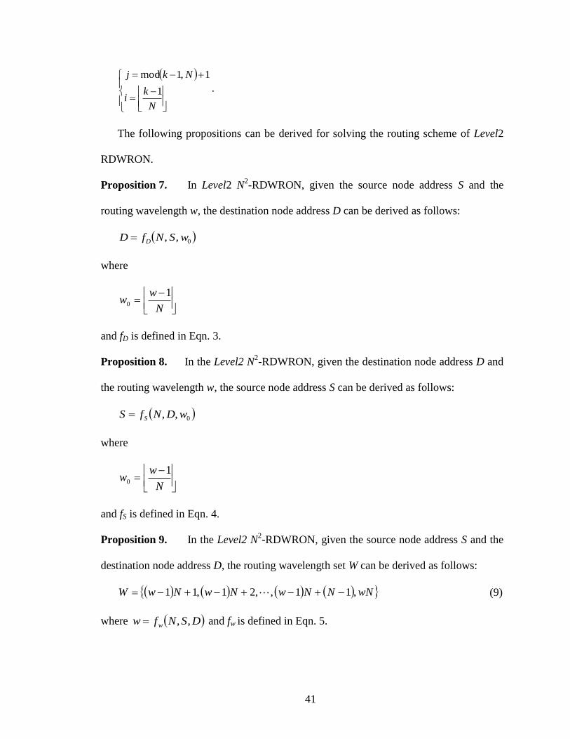
41
N
ki
Nkj
1
1,1mod
.
The following propositions can be derived for solving the routing scheme of Level2
RDWRON.
Proposition 7. In Level2 N2-RDWRON, given the source node address S and the
routing wavelength w, the destination node address D can be derived as follows:
0,, wSNfD D
where
N
ww
10
and fD is defined in Eqn. 3.
Proposition 8. In the Level2 N2-RDWRON, given the destination node address D and
the routing wavelength w, the source node address S can be derived as follows:
0,, wDNfS S
where
N
ww
10
and fS is defined in Eqn. 4.
Proposition 9. In the Level2 N2-RDWRON, given the source node address S and the
destination node address D, the routing wavelength set W can be derived as follows:
wNNNwNwNwW ,11,,21,11 (9)
where DSNfw w ,, and fw is defined in Eqn. 5.

42
4.4 Conclusion
In this chapter, based on the WRON architecture introduced in 0, a generalized
redundant wavelength routed optical micronetwork architecture RDWRON is presented
and its routing scheme is generalized.
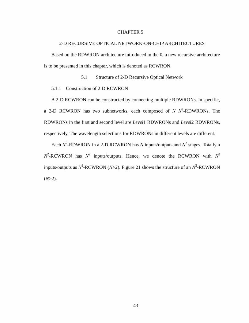
43
CHAPTER 5
2-D RECURSIVE OPTICAL NETWORK-ON-CHIP ARCHITECTURES
Based on the RDWRON architecture introduced in the 0, a new recursive architecture
is to be presented in this chapter, which is denoted as RCWRON.
5.1 Structure of 2-D Recursive Optical Network
5.1.1 Construction of 2-D RCWRON
A 2-D RCWRON can be constructed by connecting multiple RDWRONs. In specific,
a 2-D RCWRON has two subnetworks, each composed of N N2-RDWRONs. The
RDWRONs in the first and second level are Level1 RDWRONs and Level2 RDWRONs,
respectively. The wavelength selections for RDWRONs in different levels are different.
Each N2-RDWRON in a 2-D RCWRON has N inputs/outputs and N
2 stages. Totally a
N2-RCWRON has N
2 inputs/outputs. Hence, we denote the RCWRON with N
2
inputs/outputs as N2-RCWRON (N>2). Figure 21 shows the structure of an N
2-RCWRON
(N>2).

44
Figure 21 Structure of N2-RCWRON.
The connection principle of N2-RCWRON is explained as follows. The i
th output
node of the jth
N2-RDWRON is connected to the j
th input node of i
th N
2-RDWRON in the
second level.
One may notice that the structure of an N2-RCWRON is not unique. The basic rule is
that each Level1 RDWRON must have a connection to each Level2 RDWRON, and vice
versa.
Lemma 4. The total number of switches in one 2-D N2-RCWRON is
2
12
2
12
32
NNNNNORCWRON
(10)

45
5.1.2 Fault Tolerance Capability
Compared with the WRON, a distinct advantage of RCWRON is attributed to its fault
tolerance capability. As shown in Figure 21, an N2-RCWRON is composed of 2N
RDWRONs, which are independent from each other. When one path fails, the faulty
RDWRON can be easily identified by checking the sub-path in different levels of
subnetworks. By abandoning the faulty RDWRON and the input/output nodes connected
by the faulty RDWRON, the rest of the RCWRON can still operate normally.
5.2 Routing Scheme of 2-D RCWRON
The key idea of the routing scheme for the 2-D RCWRON is to decompose the
routing path into two parts, each corresponding to the sub-paths in two subnetworks,
respectively, and then solve the routing problem in each RDWRON.
In the following, we will first present the rules of assigning routing wavelengths
before we describe the routing scheme.
5.2.1 Routing Wavelength Assignment
N2 different wavelengths can be partitioned into two disjoint subsets W
(1) and W
(2).
For all Level1 RDWRONs, their assigned routing wavelengths are exclusively from W(2)
as, while for all Level2 RDWRONs, assign wavelength subsets in W(1)
as their routing
wavelengths.
For any routing path P in RCWRON with assigned wavelength w, the path can be
decomposed into two segments, P1 and P2, where P1 is the routing path in the first
subnetwork (i.e., Level1 RDWRONs) and P2 is the routing path in the second subnetwork
(i.e., Level2 RDWRONs). For P1, the routing wavelength w must be in one of the subsets
in the Partition 2, denoted as W(2)
. And for P2, the routing wavelength w must be in one of

46
the subsets in the Partition 1, denoted as W(1)
. The following lemmas elaborate how to
determine such w.
Lemma 5. Given a set W with N2 different elements, there exist at least 2
different ways to partition W into N subsets:
W = Nm
mWW,,2,1
)1()1(
and W = Nn
nWW,,2,1
)2()2(
,
where each subset has N elements such that for any two different subsets )1()1( WWm ,
)2()2( WWn (m, n=1,2,…,N), there is one and only one common element, i.e.,
)2()1(
nmmn WWw .
Lemma 6. There are totally N2 different combinations of )1(
mW and )2(nW , where
)1()1( WWm , )2()2( WWn (m, n=1,2,…,N). All N
2 common elements for the N
2
combinations of )1(
mW and )2(
nW are different from each other and these common elements
compose the N2 different elements of set W.
Lemmas 5 and 6 can be proved as follows.
Proof: Assume that W = {wt, t = 1,2,…,N2}, then an N×N matrix M can be generated as
M(i,j) = wt if t = (i - 1) × N+j, 1 ≤ i, j ≤ N,
where i and j denote the row and column number in M, respectively.
The two partitions of W can be obtained as follows.
W = NmNm
m NjjmMWW,,2,1,,2,1
)1()1( ,,2,1,
and
W = NnNn
n NiniMWW,,2,1,,2,1
)2()2( ,,2,1,
.
It is easy to see that the subset 1
mW in )1(W and the subset 2
nW in )2(W correspond

47
to the mth
row and the nth
column in M, respectively. The mth
row and the nth
column in M
must intersect at the element M(m, n) = wt, where t = (m-1) × N + n, which corresponds to
that subsets 1
mW and 2
nW must have one and only one common element
21
nmmn WWw = wt.
Conversely, each element in M, M(m, n) = wt, is uniquely identified by its coordinate
(m, n), which corresponds to the common element of the unique combination of
21 , nm WW .
Hence, Lemma 5 and Lemma 6 hold. ■
One of the simplest ways to partition set W ={1,2,…,N2} into 2 different subset
groups which satisfy Lemmas 5 and 6 are:
Partition 1:
W
NmNmm NiiNmW
,,2,1,,2,1
1 ,,2,11
Partition 2:
W
NnNnn NjNjnW
,,2,1,,2,1
2 ,,2,11
It is easy to verify that Partitions 1 and 2 are just the redundant routing wavelength
subsets of Level2 and Level1 RDWRONs, respectively. According to Lemma 5, 1
mW and
2
nW has one and only one common element 21
nm WWw . Then w is the only
wavelength which can be used to route for path P.
5.2.2 Routing Scheme for RCWRON
The following notations are used in our discussion.
S (1≤S≤N2): the source node address of an N
2-RCWRON.
D (1≤D≤N2): the destination node address of an N
2-RCWRON.
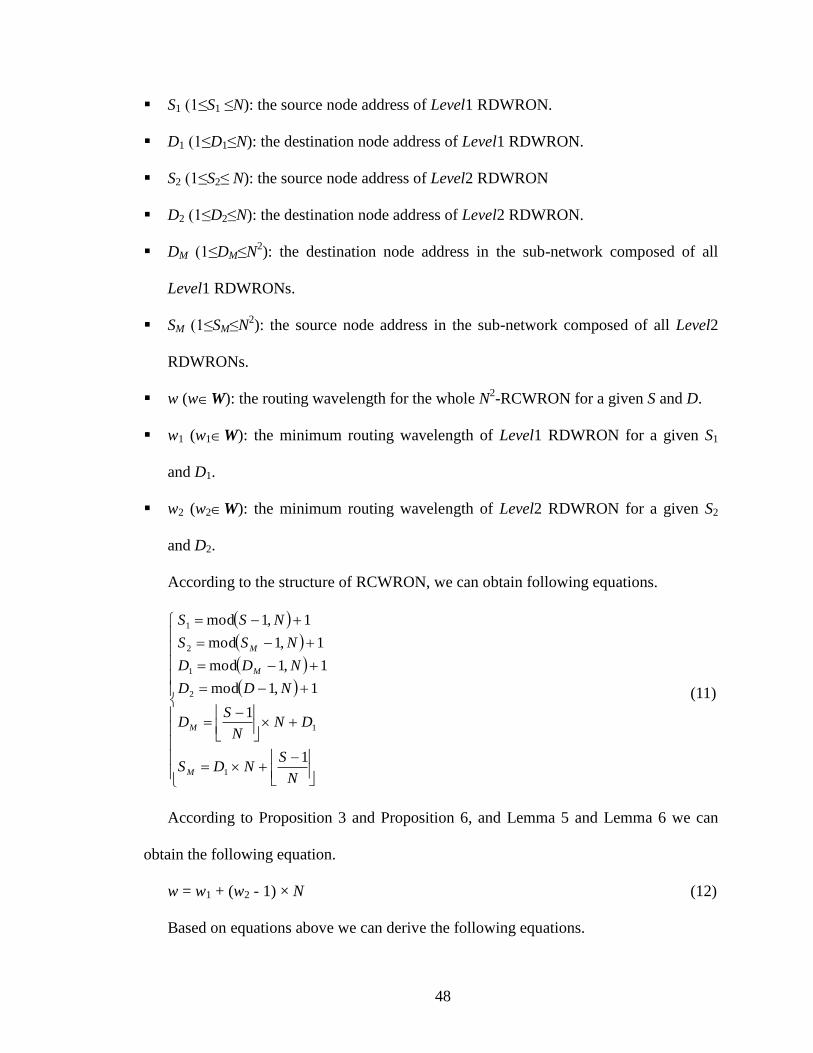
48
S1 (1≤S1 ≤N): the source node address of Level1 RDWRON.
D1 (1≤D1≤N): the destination node address of Level1 RDWRON.
S2 (1≤S2≤ N): the source node address of Level2 RDWRON
D2 (1≤D2≤N): the destination node address of Level2 RDWRON.
DM (1≤DM≤N2): the destination node address in the sub-network composed of all
Level1 RDWRONs.
SM (1≤SM≤N2): the source node address in the sub-network composed of all Level2
RDWRONs.
w (wW): the routing wavelength for the whole N2-RCWRON for a given S and D.
w1 (w1W): the minimum routing wavelength of Level1 RDWRON for a given S1
and D1.
w2 (w2W): the minimum routing wavelength of Level2 RDWRON for a given S2
and D2.
According to the structure of RCWRON, we can obtain following equations.
N
SNDS
DNN
SD
NDD
NDD
NSS
NSS
M
M
M
M
1
1
1,1mod
1,1mod
1,1mod
1,1mod
1
1
2
1
2
1
(11)
According to Proposition 3 and Proposition 6, and Lemma 5 and Lemma 6 we can
obtain the following equation.
w = w1 + (w2 - 1) × N (12)
Based on equations above we can derive the following equations.

49
N
ww
Nww
N
DD
NDD
N
SS
NSS
1
1,1mod
1
1,1mod
1
1,1mod
2
1
2
1
2
1
(13)
and
222
111
222
111
222
111
,,
,,
,,
,,
,,
,,
DSNfw
DSNfw
wDNfS
wDNfS
wSNfD
wSNfD
W
W
S
S
D
D
(14)
Then we have the following results for determining the routes in N2-RCWRON.
Proposition 10. For an N2-RCWRON, given the source node address S and routing
wavelength w, the destination node address D can be derived as
D = D2 + (D1 - 1) × N (15)
where
222
111
2
1
2
1
,,
,,
1
1,1mod
1
1,1mod
wSNfD
wSNfD
N
ww
Nww
N
SS
NSS
D
D
(16)
The function fD in Proposition 10 is given by Eqn. 3.
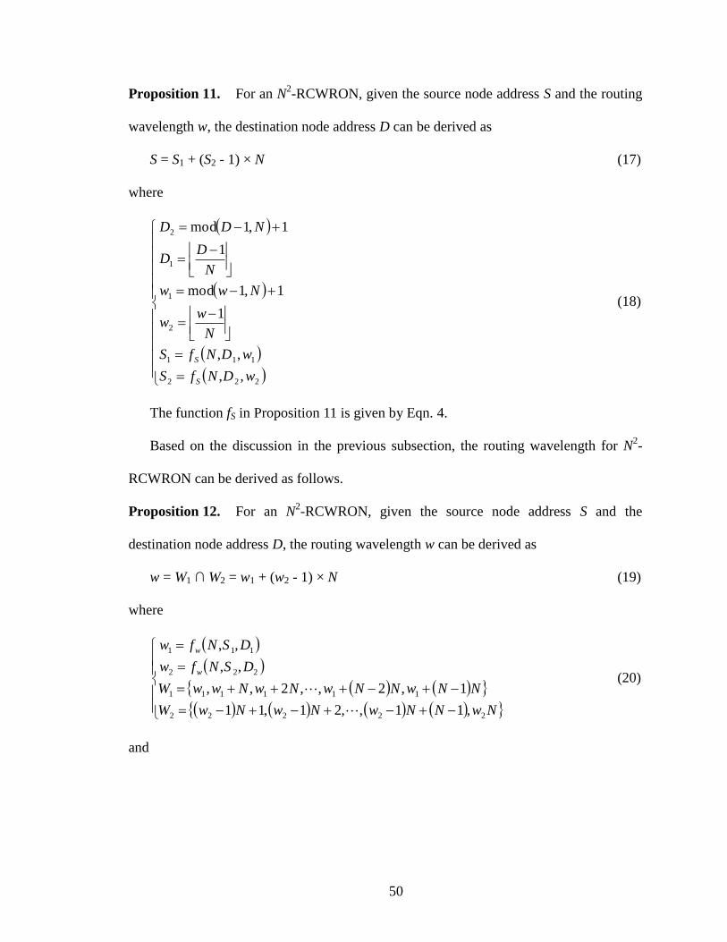
50
Proposition 11. For an N2-RCWRON, given the source node address S and the routing
wavelength w, the destination node address D can be derived as
S = S1 + (S2 - 1) × N (17)
where
222
111
2
1
1
2
,,
,,
1
1,1mod
1
1,1mod
wDNfS
wDNfS
N
ww
Nww
N
DD
NDD
S
S
(18)
The function fS in Proposition 11 is given by Eqn. 4.
Based on the discussion in the previous subsection, the routing wavelength for N2-
RCWRON can be derived as follows.
Proposition 12. For an N2-RCWRON, given the source node address S and the
destination node address D, the routing wavelength w can be derived as
w = W1 ∩ W2 = w1 + (w2 - 1) × N (19)
where
NwNNwNwNwW
NNwNNwNwNwwW
DSNfw
DSNfw
w
w
22222
111111
222
111
,11,,21,11
1,2,,2,,
,,
,,
(20)
and

51
N
DD
NDD
N
SS
NSS
1
1,1mod
1
1,1mod
1
2
2
1
(21)
The function fw in Proposition 12 is given by Eqn. 5.
5.2.3 One Routing Example
Here we use 42-RCWRON as an example to illustrate the routing scheme. Figure 22
shows the structure of Level1 42-RDWRON and Level2 4
2-RDWRON. The structure of
the 42-RCWRON is shown in Figure 23.
(a) Level1 42-RDWRON
(b) Level2 42-RDWRON
Figure 22 Structures of 42-RDWRON.
52
Figure 23 Structures of 42-RCWRON.
The routing wavelength assignment for Level1 and Level2 RDWRON are shown in
Table 4 and Table 5, respectively. The routing wavelength assignment for the whole 42-
RCWRON is given in Table 6.

53
Table 4 Routing wavelengths for Level1 42-RDWRON.
w D1 D2 D3 D4
S1 w1 w5 w9 w13 w4 w8 w12 w16 w2 w6 w10 w14 w3 w7 w11 w15
S2 w4 w8 w12 w16 w3 w7 w11 w15 w1 w5 w9 w13 w2 w6 w10 w14
S3 w2 w6 w10 w14 w1 w5 w9 w13 w3 w7 w11 w15 w4 w8 w12 w16
S4 w3 w7 w11 w15 w2 w6 w10 w14 w4 w8 w12 w16 w1 w5 w9 w13
Table 5 Routing wavelengths for Level2 42-RDWRON.
w D1 D2 D3 D4
S1 w1 w2 w3 w4 w13 w14 w15 w16 w5 w6 w7 w8 w9 w10 w11 w12
S2 w13 w14 w15 w16 w9 w10 w11 w12 w1 w2 w3 w4 w5 w6 w7 w8
S3 w5 w6 w7 w8 w1 w2 w3 w4 w9 w10 w11 w12 w13 w14 w15 w16
S4 w9 w10 w11 w12 w5 w6 w7 w8 w13 w14 w15 w16 w1 w2 w3 w4
Table 6 Routing wavelengths of 42×4
2RCWRON
Wave-
length
Desti-
nation LEVEL2 UNIT1 LEVEL2 UNIT2 LEVEL2 UNIT3 LEVEL2 UNIT4
Source w D1 D2 D3 D4 D1 D2 D3 D4 D1 D2 D3 D4 D1 D2 D3 D4
LEVEL1
UNIT1
S1 w1 w13 w5 w9 w4 w16 w8 w12 w2 w14 w6 w10 w3 w15 w7 w11
S2 w4 w16 w8 w12 w3 w15 w7 w11 w1 w13 w5 w9 w2 w14 w6 w10
S3 w2 w14 w6 w10 w1 w13 w5 w9 w3 w15 w7 w11 w4 w16 w8 w12
S4 w3 w15 w7 w11 w2 w14 w6 w10 w4 w16 w8 w12 w1 w13 w5 w9
LEVEL1
UNIT2
S1 w13 w9 w1 w5 w16 w12 w4 w8 w14 w10 w2 w6 w15 w11 w3 w7
S2 w16 w12 w4 w8 w15 w11 w3 w7 w13 w9 w1 w5 w14 w10 w2 w6
S3 w14 w10 w2 w6 w13 w9 w1 w5 w15 w11 w3 w7 w16 w12 w4 w8
S4 w15 w11 w3 w7 w14 w10 w2 w6 w16 w12 w4 w8 w13 w9 w1 w5
LEVEL1
UNIT3
S1 w5 w1 w9 w13 w8 w4 w12 w16 w6 w2 w10 w14 w7 w3 w11 w15
S2 w8 w4 w12 w16 w7 w3 w11 w15 w5 w1 w9 w13 w6 w2 w10 w14
S3 w6 w2 w10 w14 w5 w1 w9 w13 w7 w3 w11 w15 w8 w4 w12 w16
S4 w7 w3 w11 w15 w6 w2 w10 w14 w8 w4 w12 w16 w5 w1 w9 w13
LEVEL1
UNIT4
S1 w9 w5 w13 w1 w12 w8 w16 w4 w10 w6 w14 w2 w11 w7 w15 w3
S2 w12 w8 w16 w4 w11 w7 w15 w3 w9 w5 w13 w1 w10 w6 w14 w2
S3 w10 w6 w14 w2 w9 w5 w13 w1 w11 w7 w15 w3 w12 w8 w16 w4
S4 w11 w7 w15 w3 w10 w6 w14 w2 w12 w8 w16 w4 w9 w5 w13 w1
5.3 Conclusion
Based on WRON, a new 2-D Recursive Wavelength Routed Optical Network is

54
presented in this chapter which is suitable for ONoC. The 2-D RCWRON is constructed
by using 2-D RDWRONs. The routing scheme for 2-D RCWRON is derived based on
the routing scheme for 2-D RDWRON.
The major advantage of the proposed 2-D RCWRON over the WRON is its fault-
tolerance capability at a relatively high construction cost.

55
CHAPTER 6
QUARTERED RECURSIVE DIAGNAL TORUS NETWORK-ON-CHIP
ARCHITECTURES
Network-on-a-chip (NoC) is an effective approach to connect and manage the
communication between the variety of design elements and intellectual property blocks
required in large and complex system-on-chips. In this chapter a new NoC architecture is
propose, referred as the Quartered Recursive Diagonal Torus (QRDT), which is
constructed by overlaying diagonal torus. Due to its small diameter and rich routing
recourses, QRDT is determined to be well suitable to construct highly scalable NoCs. In
QRDT, data packets can be routed through a proposed minimal routing algorithm based
on the Johnson codes that have traditionally been used in finite state machine designs. It
has been shown that this proposed routing algorithm with minor modifications is capable
of handling the single link/node failure.
The advance ONoC architectures going to be introduced in the next two chapters are
based on the WRON introduced in Chapter 1 and QRDT to be introduced in this chapter.
6.1 Introduction
The development of VLSI technology has continuously driven the increase of on-chip
capacity. The International Technology Roadmap for Semiconductors (ITRS) predicts
that System-on-Chips (SoCs) will grow to multi-billion transistors in next a few years [1].
One of the major challenges in designing such highly integrated SoCs will be to find an
effective way to integrate multiple pre-designed Intellectual Property (IP) cores while
addressing pressing power and performance concerns [75]. With a communication centric
design style, Networks-on-Chips (NoCs) have emerged as a new SoC paradigm [75] to

56
overcome the limitations of bus-based communication infrastructure.
In general, a packet-based NoC consists of routers, the network interface between the
router and the IP, and the interconnection network. The major challenges imposed upon
NoC designs include scalability, energy efficiency, and reconfigurability [76]. Numerous
interconnection network topologies have been considered for NoCs, including mesh [77],
torus [78], fat tree [79], honeycomb, and quite a few others [76]. However, these
interconnection topologies either scale poorly or have no support for reconfigurability. To
address these two problems, a class of topologies named Recursive Diagonal Torus (RDT)
has made its way to NoC designs [80].
An RDT structure is constructed by recursively overlaying 2-D diagonal torus [77],
and it has the following features: recursive structure with constant node degree, smaller
diameter and average distance, and embedded mesh/torus topology. Consider a torus
network composed of N×N nodes, where N = nk and both n and k are natural numbers.
The rank-0 torus is formed by creating a link between node (x, y) and each of its
neighboring four nodes: (mod(x ± 1, N), y) and (x, mod(y ± 1, N)). On top of rank-0 torus,
rank-1 torus is formed by adding one link between node (x, y) and each of the four nodes
(mod(x ± n, N), mod(y ± n, N)) it needs to connect to. The direction of the rank-1torus is
at an angle of 45 degrees to the rank-0 torus. On rank-1 torus, rank-2 torus can be formed
by adding 4 links to a node in the same manner. In a more general sense, a rank-(r+1)
torus is formed upon rank-r torus.
In this chapter, a special type of RDT structure, Quartered RDT (QRDT) will be
presented. The QRDT architecture exhibits a number of desirable networking properties
that make it particularly appreciated in building large on-chip micro-networks. By

57
indexing the network nodes with the Johnson codes, a new minimal routing algorithm,
named Johnson Coded Vector Routing (JCVR), is proposed for QRDT. The JCVR
algorithm with minor modifications is capable of routing data packets when there is a
single link/node failure in a QRDT-based NoC.
6.2 QRDT Structure and Its Network Properties
As a special type of RDT, the QRDT network is also constructed by overlaying
diagonal torus. An N-QRDT has N×N nodes where N=4n and n is a positive integer. A
QRDT is composed of nodes, rank-0 links, and rank-1 links. Each node (x, y), where 0≤x,
y≤N-1, in the QRDT has 4 rank-0 links connecting to its four neighbors (mod(x ± 1, N), y)
and (x, mod(y ± 1, N)) on rank-0 torus, and 4 rank-1 links connecting to its another four
neighbors (mod(x n, N), mod(y n, N)) on rank-1 torus. In total, an N-QRDT has N2
nodes and 4N2 links. Figure 24 shows the structure of 4-QRDT.
Figure 25 (a) shows the directions of the 8 channels, and each channel is labeled by
the dimension, rank number, and direction. Figure 25 (b) shows the coordinates of all
eight nodes that are connected to node (x, y) through respective channels shown in Figure
25 (a).

58
(0,0) (1,0) (2,0)
(3,0)
(0,1)
(1,1)
(1,2)
(1.3)
(0,2) (1,2)
(2,2) (3,2)
(0,3) (1,3) (2,3) (3,3)
Figure 24 Structure of 4-QRDT.
X0 - X0 +
Y0 -
X1 - Y1 -
X1 + Y1 +
Y0 +
(a) Directions of 8 channels.

59
(mod(x+1,N),y)
(x,mod(y-1,N))
(x,y)
(mod(x-n,N),mod(y-n,N)) (mod(x+n,N),mod(y-n,N))
(mod(x+n,N),mod(y+n,N))(mod(x-n,N),mod(y+n,N))
(x,mod(y+1,N))
(b) Coordinates of 8 nodes connected to node (x, y) through these channels
Figure 25 Channeling in QRDT
Lemma 7. The diameter of the N-QRDT network is n+1, where n=N/4.
Lemma 8. The average distance of the N-QRDT is
116
23
3220
3
32
2
23
n
nnn
(22)
where n=N/4.
The complete proof of Lemma 7 and Lemma 8, based on the routing algorithm to be
presented in Section 6.4, are provided in the Appendix 0
Table 7 lists the diameters and the average distances of QRDT, mesh, torus, and
hypercube with different network sizes. One can see that QRDT has smaller diameter and
average distance than the other three structures for most network sizes.

60
Table 7 Different networks‟ diameter (R) and average distance (AD)
Network
Size
QRDT Mesh Torus Hypercube
R AD R AD R AD R AD
4×4 2 1.47 6 2.67 4 2 4 2
8×8 3 2.31 14 5.33 8 4 6 3
16×16 5 3.77 30 10.67 16 8 8 4
32×32 9 6.51 62 21.33 32 16 10 5
As QRDT is a special type of RDT structure, the Vector Routing (VR) algorithm
proposed for RDT can be readily applied to QRDT. The goal of the vector routing
algorithm is to represent the routing vector with an expression that combines all unit
vectors in rank-0 and rank-1 torus and the hop counts. However, the vector routing
algorithm cannot guarantee it is minimal routing (i.e., the number of hops on the routing
path may not be minimum). A minimal routing algorithm, named Johnson coded vector
routing algorithm is to be explained in the following. The Johnson codes are introduced
first before the JCVR algorithm is described.
6.3 Johnson Codes and Functions to Manipulate the Codes
6.3.1 Johnson Codes
The m-bit Johnson code has M (M = 2m) code words, and it can be denoted as
121210 ,,,,,,,, MMii CCCCCCC
where code word Ci is given as
im
i
m
i
j
i
j
i
j
ii
i bbbbbbbC 121110
and
mjim
mjiormjib i
j21
20

61
For example, the eight 4-bit Johnson code words are 0000, 0001, 0011, 0111, 1111,
1110, 1100 and 1000.
On the other hand, given an m-bit Johnson code word Ci, i can be determined by the fa
function as
1
0
0
1
0
0
1
0
im
j
i
j
im
j
i
j
ia
bifbm
bifb
Cfi (23)
6.3.2 Basic Functions of Johnson Codes
Two basic functions of Johnson codes are defined: the distance function and the
direction function. These functions will be used in the JCVR algorithm.
The distance function is used to determine the Hamming distance between two
Johnson-codes. Given two m bits Johnson-codes: A and B, where A= a0a1a2…am-1 and B
= b0b1b2…bm-1, the distance p between them is
1
0
m
iii bap (24)
The direction function is used to determine the output direction. The direction c is
calculated as:
Case 1: p = 0, then c = 0
Case 2: a0 = 0 and b0 = 0, then
1
0
1
0
1
0
1
0
1
1
m
ii
m
ii
m
ii
m
ii
abif
abifc (25)
Case 3: a0 = 1 and b0 = 1, then

62
1
0
1
0
1
0
1
0
1
1
m
ii
m
ii
m
ii
m
ii
abif
abifc (26)
Case 4: a0 = 0 and b0 = 1, then
1
0
1
0
1
0
1
0
1
1
m
ii
m
ii
m
ii
m
ii
abif
abifc (27)
Case 5: a0 = 1 and b0 = 0, then
1
0
1
0
1
0
1
0
1
1
m
ii
m
ii
m
ii
m
ii
abif
abifc (28)
For simplicity, the calculation of the distance and direction can be denoted as one
function fr as
BAfcp r ,, (29)
6.4 Routing Algorithm for QDRT
6.4.1 JCVR Algorithm
The routing steps from a source node to its destination node can be derived as
,00001111 YvecYXvecXYvecYXvecXA
where 1X
, 1Y
, 0X
, and 0Y
are the unit
vectors in rank-1 torus and rank-0 torus (with their directions shown in Figure 25 (a)) and
their respective coefficients, vecX1, vecY1, vecX0, vecY0, give the number of hops on
corresponding dimensions.
In the JCVR algorithm, the coefficients for the unit vectors are calculated at the
source node. For N-QRDT, given the source and the destination addresses S=(Sx, Sy),
D=(Dx, Dy), where Sx and Sy (Dx and Dy) represent the X and Y coordinates of the source

63
(destination) node in m-bit (m=N/2) Johnson code, respectively. The direction and
distance values of the two coordinates, (px, cx) and (py, cy), can be determined by
calculating fr as discussed in Section 3.2.
The address of each intermediate node M = (Mx, My) on the routing path from S to D
is given as,
0mod
0mod,,
0mod
0mod,,
yyN
yyN
yysy
xxN
xxN
xxsx
cwhennS
cwhennSNcSfM
cwhennS
cwhennSNcSfM
(30)
The JCVR algorithm for QRDT is presented in Figure 26.
Figure 26 Vector routing algorithm for QRDT.
Vector Routing Algorithm for QRDT:
begin
initialize vecX0, vecY0, vecX1, vecY1 to zero
set Mx=Sx, My=Sy
while (Dx≠Mx and Dy≠My) do
calculate (px, cx) and (py, cy) using fr function
if (cx=0 and cy=0) then set vecX0, vecY0, vecX1, vecY1 to zero
elseif (px+py≤n) then
if (cx≥0) then vecX0=vecX0 + px
elseif (cx<0) then vecX0=vecX0–px
if (cy≥0) then vecY0=vecY0+py
elseif (cy<0) then vecY0=vecY0–py
go to end
elseif (px+py>n) then
if (cx≥0 and cy≥ 0) then vecX1=vecX1+1
if (cx≥0 and cy<0) then vecY1=vecY1–1
if (cx<0 and cy≥0) then vecY1=vecY1+1
if (cx<0 and cy<0) then vecX1=vecX1–1
calculate Mx and My using the fs function
endif
endwhile
end

64
For an N-QRDT, the while loop will be executed no more than m=N/4 times to
complete the calculation of the four coefficients (vecX1, vecY1, vecX0, vecY0).
At the source node, the four coefficients are computed and encapsulated into the
packet. At the source node and each intermediate node, the coefficients for the unit
vectors will be checked in a default order of vecX1, vecY1, vecX0, vecY0. The packet will
be routed to the direction as determined by the first unit vector with non-zero coefficient
(hop count) and this vector‟s coefficient, depending on the routing direction (+/-), will be
decreased/increased before the data packets are actually forwarded to the next hop
towards the destination.
Compared to the VR algorithm, the advantage of the JCVR algorithm is that it can
achieve minimal routing (as proved in Lemma 7), which is not guaranteed in VR.
6.4.2 Fault Tolerance Routing for QRDT under Single Link/Node Failure
It has been well recognized that fault-tolerance capability is vital for a NoC system
[81], since one faulty link/processor may isolate a large fraction of IP cores from being
reachable by other cores. Next we show that with minor modification, the JCVR
algorithm is capable of handling single link/node failure.
The following assumptions are made first:
Any link or node in the network can fail, and the faulty components are unusable; that
is, data will not be transmitted over a faulty link or routed through a faulty node.
The fault model is static; that is, no new faults occur during a routing process.
Both source and destination nodes (on rank-0 or rank-1 torus) are fault-free.
The faults occur independently.
If a node fails, all the eight links associated with the node on rank-0/1 tori are

65
considered unusable.
During the routing process, when the next routing link/node is found to be faulty in a
QRDT network, fault-tolerance routing can be realized dynamically as described below.
The faulty link encountered must be on one of the four dimensions (i.e., 1X
, 1Y
, 0X
, and
0Y
). There are two cases to consider:
Case 1: if there exists one or more other dimensions with non-zero coefficient, the
routing steps on such dimension(s) will be completed first followed by the routing
steps on the dimension with faulty link/node.
Case 2: otherwise, one step on the dimension on the same rank and orthogonal to the
dimension with faulty link/node will be completed first followed by the routing steps
on the dimension with faulty link/node and one opposite routing step on the
orthogonal dimension.
Figure 27 (a) shows an example of Case 1 under single link failure. The detoured
routing path is S-M0-M1-D, which does not introduce extra hops compared to the original
routing path S-M0-M2-D. Similarly, as shown in Figure 28 (a), no extra hop is introduced
on the detoured routing path for such a case under single node failure.

66
(a) Case1 (b) Case2
Figure 27 Two cases under single link fault.
Figure 27 (b) shows an example of Case 2 with a single link failure, where the
detoured routing path has two extra hops than the original routing path. As shown in
Figure 28 (b), the number of extra hops on the detoured routing path is also two for such
a case under single node failure.
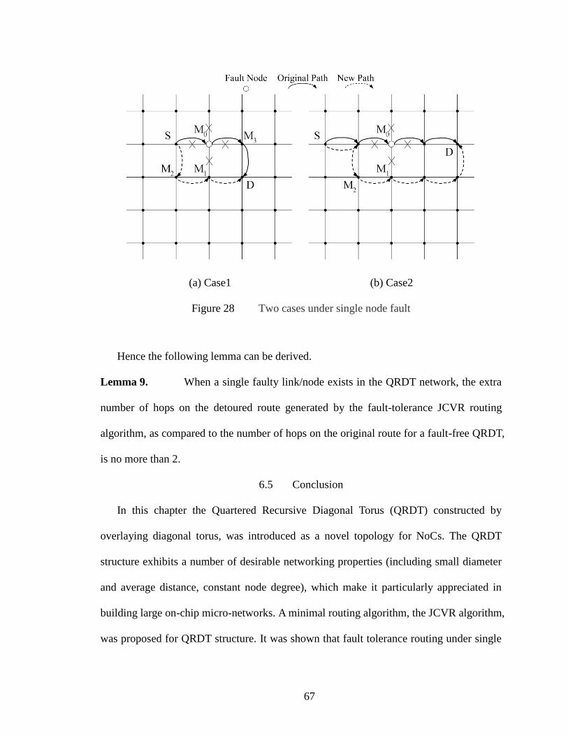
67
(a) Case1 (b) Case2
Figure 28 Two cases under single node fault
Hence the following lemma can be derived.
Lemma 9. When a single faulty link/node exists in the QRDT network, the extra
number of hops on the detoured route generated by the fault-tolerance JCVR routing
algorithm, as compared to the number of hops on the original route for a fault-free QRDT,
is no more than 2.
6.5 Conclusion
In this chapter the Quartered Recursive Diagonal Torus (QRDT) constructed by
overlaying diagonal torus, was introduced as a novel topology for NoCs. The QRDT
structure exhibits a number of desirable networking properties (including small diameter
and average distance, constant node degree), which make it particularly appreciated in
building large on-chip micro-networks. A minimal routing algorithm, the JCVR algorithm,
was proposed for QRDT structure. It was shown that fault tolerance routing under single

68
link/node failure can be handled by the JCVR algorithm with minor modifications.
Compared with the VR algorithm, the JCVR algorithm achieves minimal routing. The
tradeoff is the moderately higher implementation cost of the JCVR-based router than the
VR-based router.

69
CHAPTER 7
PACKET SWITCHING OPTICAL NETWORK-ON-CHIP ARCHITECTRUES
In this chapter three packet switching optical Network-on-Chip architectures, i.e.,
TON-I, TON-II and TON-III that are built on the topology of 2D-torus are presented.
Micro-ring resonator (MRR)-based optical switches are adopted for wavelength-based
routing in TONs. The implementation of a packet switching optical NoC with a limited
number of wavelengths, the design of routers and a schema for wavelength assignment
are illustrated in detail. The proposed TON architectures explore passive MRR switching,
Wavelength Division Multiplexing (WDM) and Direct Optical Channels (DOC) yield a
high bandwidth, a low latency and a low power consumption. The architectures are also
potentially fault-tolerant. The average frame transmission time and the buffer utilization
by are evaluated with simulation. The power analysis and the transmission power losses
are provided. Simulation and analysis results show that the proposed architectures can be
considered as a viable solution for future NoCs [82, 83].
7.1 Introduction
In the three different 2D torus-based passive MRR routing packet-switching optical
NoC architectures TON-I, TON-II and TON-III, the physical interconnections of these
TONs are as in 2D-torus. However, a new concept, direct optical channels (DOC), is
proposed to build the direct light path between two nodes. A DOC consists of a set of
interconnected physical links (waveguides) and routers. With a predefined routing
wavelength, light can travel in a DOC without relay. Optical data packets can be
transmitted in the TON by relay of different DOCs.

70
7.2 TON Architectures
7.2.1 Interconnections in TON network
The TON is an NN, where N=2n, nN, 2D-torus-based network. A 66 TON
example is presented in Figure 29. Each node in the TON is denoted by a pair (x,y) where
x,y={0,1,…,N-1}. Each node has a router and a processor (core), and it is physically
connected to four adjacent nodes. Internally, each router has a wavelength routed Optical
Interconnection Unit (OIU) and an Optical Electrical Router (OER).
Router
I-OIU
I-OER
COR
E
I-Node II-Node I-Node II-Node I-Node II-Node
I-Node II-Node I-Node II-Node I-NodeII-Node
I-Node II-Node I-Node II-Node I-Node II-Node
I-Node II-Node I-Node II-Node I-NodeII-Node
I-Node II-Node I-Node II-Node I-Node II-Node
I-Node II-Node I-Node II-Node I-NodeII-Node
(3,0)
(0,0)
(1,0)
(2,0)
(5,0)
(4,0)
(3,1)
(0,1)
(1,1)
(2,1)
(5,1)
(4,1)
(3,2)
(0,2)
(1,2)
(2,2)
(5,2)
(4,2)
(3,3)
(0,3)
(1,3)
(2,3)
(5,3)
(4,3)
(3,4)
(0,4)
(1,4)
(2,4)
(5,4)
(4,4)
(3,5)
(0,5)
(1,5)
(2,5)
(5,5)
(4,5)
Figure 29 Structure of 6×6 Torus-based Optical Network-on-chip
The TON nodes are classified into two classes: I-Node associated with I-router; and
II-node with II-router. I-router has an I-OIU and an I-OER, and II-router has an II-IOU

71
and an II-OER. Given coordinates (x, y), a node is an I-Node if x + y = 2n (nN),
otherwise it is a II-Node.
OIU is an MRR matrix device designed by properly connecting MRR switches with
the waveguide. The function of OIU is the port-to-port routing of the optical signal e
based on its wavelength. OIU has six ports, of which four are external ports (S1, S2, D1,
D2), and two, i.e., (LS, LD) are internal ports to connect to the OER.
The interconnection of an 88 TON is shown in Figure 30. In (x, y) node, its S1 port
of OIU is connected to D2 port of the OIU in (x-1, y), its S2 port of OIU is connected to
D1 port of the OIU in (x, y-1); D1 port of the OIU is connected to S1 of (x, y+1) node,
and D2 is connected to S1 of the OIU of (x+1, y) node.
7.2.2 Optical Interconnection Unit (OIU)
OIU structure proposed in the paper is developed from WRON structure [54]. Unlike
to many other MRR structures such as in [14], WRON is 100% non-blocking. It is
guaranteed in WRON that lights in same wavelength will not be inducted into same
waveguide. Hence no interference will happen during the wavelength multiplexing
transmission. And much less medium access control needed, which massively simplified
the design.
7.2.3 Optical-Electrical Router (OER)
The function of an OER is to receive input optical signal, convert it to electrical data,
read its header and convert it to an optical signal in a proper wavelength and then
transmit it to the next node through a proper output channel.
An OER connects to OIU‟s LS and LD ports by two waveguides. Inside the OER,
these two waveguides connect to two couplers which mixed input/output optical signals.

72
Each coupler is connected to an optical wavelength multiplexer and a demultiplexer. If
each node has n channels, then each multiplexer converges n/2 output optical signals
from n/2 lasers to a waveguide, and each demultiplexer diverges n/2 input optical signals
from a waveguide to n/2 photo-detectors. Each laser/photo-detector is connected to a
crossbar switch via an output port/input buffer. And there is a local output port/input
buffer which is also connected to the crossbar switch for handling data to/from the core.
7.2.4 Directed Optical Channel (DOC)
Data transmission in the TON is implemented via a DOC. The DOC is a realization of
the channel with a light path between two nodes that consists of one or more physical
links and OIUs. By utilizing a predetermined routing wavelength and with properly
designed OIUs light can travel through the DOC without any relay or arbitration. DOCs
can be placed between any two nodes. Examples of one-hop and two-hop DOCs in the
88 TON are shown in Figure 30.
Two nodes which do not have a DOC will exchange data packets by relaying in
intermediary nodes. This would require electrical/optical and optical/electrical (E/O &
O/E) conversion. Data transmission latency is directly related to the number of such
conversions.

73
Figure 30 Structure of 8×8 TON and DOC examples.
7.3 TON-I Architecture
7.3.1 TON-I Topology
Each node in the network is directly connected to four other nodes via four DOCs.
Given a node (x,y), its channel map is shown in Figure 31. Its channels are:

74
E1: (x,y) (x,y+1); W1: (x,y) (x,y-1); S1(x,y) (x+1,y); N1: (x,y) (x-1,y);
Figure 31 TON-I network topology
7.3.2 Channel Realization
As mentioned before, channels in TON network are realized with DOC. Four
channels shown in Figure 31 can be realized with DOC as explained in Table 8.
Table 8 Channel Realization in TON-I
C. W. S. D. P. C. DOC
E1 w1 (x,y) (x,y+1) LS E (x,y)LS(x,y)D1(x,y+1)S2(x,y+1)LD*
S1 w2 (x,y) (x+1,y) LS S (x,y)LS(x,y)D2(x+1,y)S1(x+1,y)LD
W1 w1 (x,y) (x,y-1) LD W (x,y)LD(x,y)S2(x,y-1)D1(x,y-1)LS
N1 w2 (x,y) (x-1,y) LD N (x,y)LD(x,y)S1(x-1,y)D2(x-1,y)LS
* „ ‟represents the routing with optical resonator switching inside OIU, „ ‟
represents the routing with waveguide links between OIUs.

75
7.3.3 Routing Table of OIUs in TON-I
The routing truths of I-OIU and II-OIU in TON-I are identical, as shown in Table 9.
Table 9 Routing truth table of OIUs in TON-I
Port w1 w2
LS D1 D2
LD S2 S1
7.3.4 OIUs in TON-I
The structure of I-OIU and II-OIU in TON-I are identical. It can be constructed
according to Table 9, as shown in Figure 32.
Figure 32 OIU structure of TON-I
7.3.5 OERs in TON-I
Based on the routing pattern shown in Table 8, the OER in TON-I can be designed
and that is displayed in Figure 33.
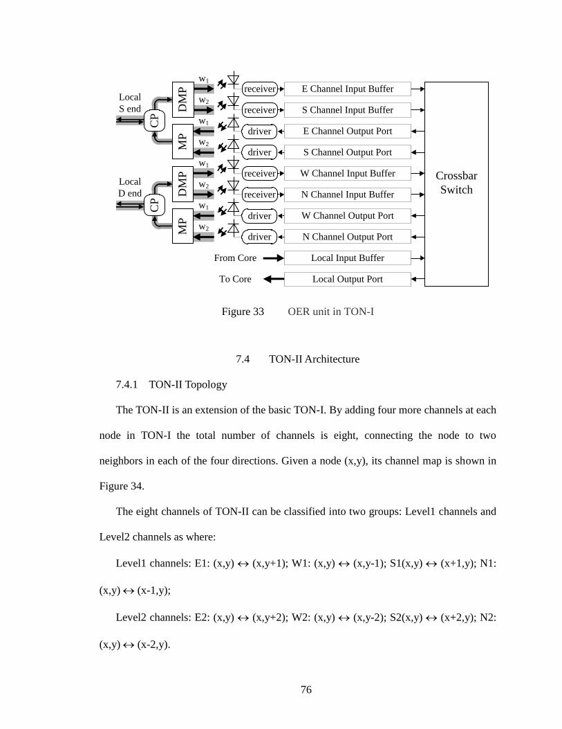
76
Crossbar
Switch
From Core
To Core
Local
S end
w2
driver
w1
driver
w1
w2D
MP receiver
receiver
Local Input Buffer
Local Output Port
N Channel Input Buffer
W Channel Input Buffer
E Channel Output Port
S Channel Output Port
w1
w2
DM
P receiver
receiver S Channel Input Buffer
E Channel Input Buffer
w2MP
driver
w1
driver W Channel Output Port
N Channel Output Port
CP
MP
Local
D end
CP
Figure 33 OER unit in TON-I
7.4 TON-II Architecture
7.4.1 TON-II Topology
The TON-II is an extension of the basic TON-I. By adding four more channels at each
node in TON-I the total number of channels is eight, connecting the node to two
neighbors in each of the four directions. Given a node (x,y), its channel map is shown in
Figure 34.
The eight channels of TON-II can be classified into two groups: Level1 channels and
Level2 channels as where:
Level1 channels: E1: (x,y) (x,y+1); W1: (x,y) (x,y-1); S1(x,y) (x+1,y); N1:
(x,y) (x-1,y);
Level2 channels: E2: (x,y) (x,y+2); W2: (x,y) (x,y-2); S2(x,y) (x+2,y); N2:
(x,y) (x-2,y).
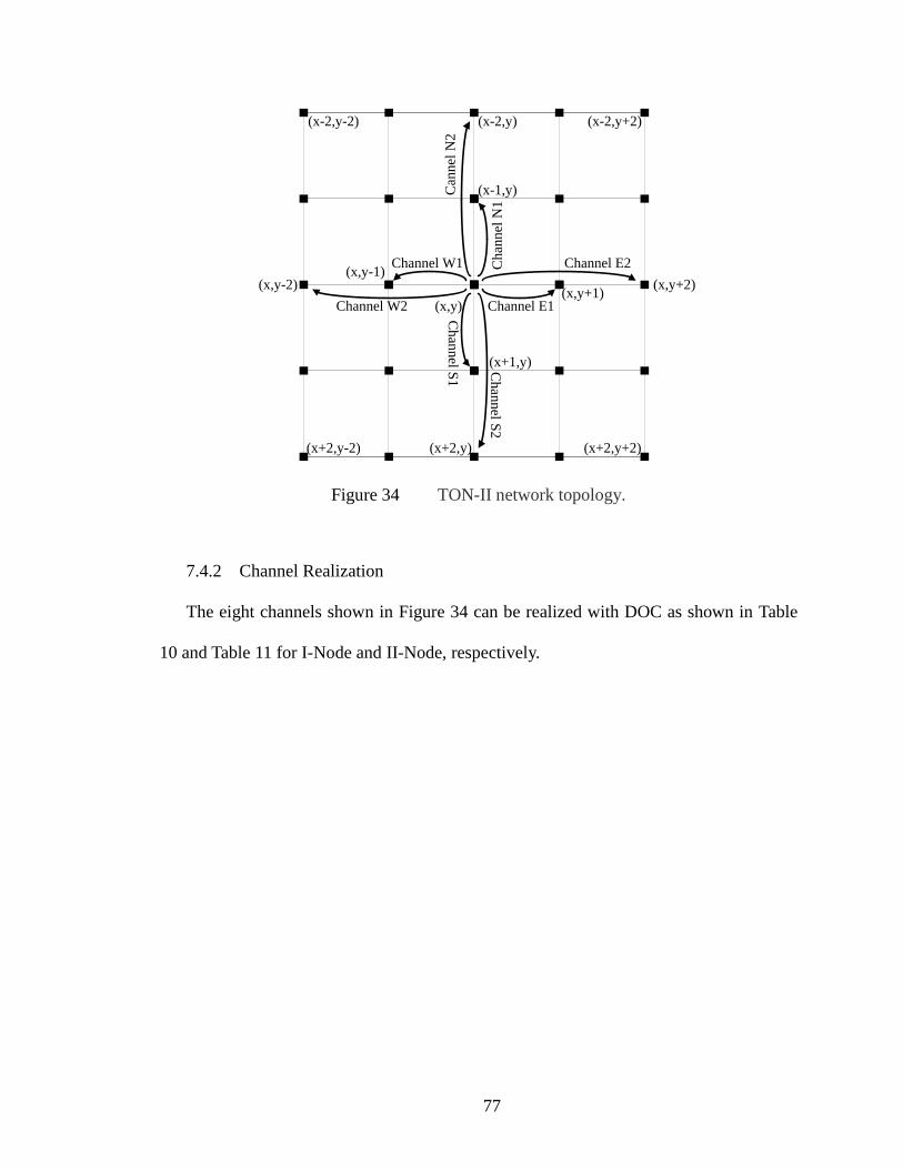
77
(x,y)
(x,y-1)
(x,y+1)
(x-1,y)
(x+1,y)
Channel E1
Ch
ann
el S1
Channel W1 Chan
nel
N1
(x,y-2) (x,y+2)
Channel E2
(x-2,y)
Can
nel
N2
Channel W2
Chan
nel S
2
(x+2,y)
(x-2,y-2) (x-2,y+2)
(x+2,y+2)(x+2,y-2)
Figure 34 TON-II network topology.
7.4.2 Channel Realization
The eight channels shown in Figure 34 can be realized with DOC as shown in Table
10 and Table 11 for I-Node and II-Node, respectively.

78
Table 10 Channel Realization for I-Node in TON-II
C. W. S. D. P. Routing Path
E1 w1 (x,y) (x,y+1) LS (x,y)LS(x,y)D1(x,y+1)S2(x,y+1)LD
E2 w2 (x,y) (x,y+2) LS (x,y)LS(x,y)D1(x,y+1)S2(x,y+1)D1
(x,y+2)S2(x,y+2)LD
S2 w3 (x,y) (x+2,y) LS (x,y)LS(x,y)D2(x+1,y)S1(x+1,y)D2
(x+2,y)S1(x+2,y)LD
S1 w4 (x,y) (x+1,y) LS (x,y)LS(x,y)D2(x+1,y)S1(x+1,y)LD
W1 w1 (x,y) (x,y-1) LD (x,y)LD(x,y)S2(x,y-1)D1(x,y-1)LS
W2 w2 (x,y) (x,y-2) LD (x,y)LD(x,y)S2(x,y-1)D1(x,y-1)S2
(x,y-2)D1(x,y-2)LS
N2 w3 (x,y) (x-2,y) LD (x,y)LD(x,y)S1(x-1,y)D2(x-1,y)S1
(x-2,y)D2(x-2,y)LS
N1 w4 (x,y) (x-1,y) LD (x,y)LD(x,y)S1(x-1,y)D2(x-1,y)LS
Table 11 Channel Realization for II-Node in TON-II
C. W. S. D. P. Routing Path
E1 w1 (x,y) (x,y+1) LS (x,y)LS(x,y)D1(x,y+1)S2(x,y+1)LD
S2 w2 (x,y) (x+2,y) LS (x,y)LS(x,y)D2(x+1,y)S1(x+1,y)D2
(x+2,y)S1(x+2,y)LD
E2 w3 (x,y) (x,y+2) LS (x,y)LS(x,y)D1(x,y+1)S2(x,y+1)D1
(x,y+2)S2(x,y+2)LD
S1 w4 (x,y) (x+1,y) LS (x,y)LS(x,y)D2(x+1,y)S1(x+1,y)LD
W1 w1 (x,y) (x,y-1) LD (x,y)LD(x,y)S2(x,y-1)D1(x,y-1)LS
N2 w2 (x,y) (x-2,y) LD (x,y)LD(x,y)S1(x-1,y)D2(x-1,y)S1
(x-2,y)D2(x-2,y)LS
W2 w3 (x,y) (x,y-2) LD (x,y)LD(x,y)S2(x,y-1)D1(x,y-1)S2
(x,y-2)D1(x,y-2)LS
N1 w4 (x,y) (x-1,y) LD (x,y)LD(x,y)S1(x-1,y)D2(x-1,y)LS
7.4.3 Routing Table of OIUs in TON-II
According to the DOC realization shown in Table 10 and Table 11, the routing truths
of I-OIU and II-OIU in TON-II can be derived as in Table 12 and Table 13.

79
Table 12 Routing truth table of I-OIU in TON-II
w1 w2 w3 w4
LS D1 D1 D2 D2
S1 D2 D2 LD LD
S2 LD LD D1 D1
Table 13 Routing truth table of II-OIU in TON-II
w1 w2 w3 w4
LS D1 D2 D1 D2
S1 D2 LD D2 LD
S2 LD D1 LD D1
7.4.4 OIUs in TON-II
The structure of the I-OIU and II-OIU in TON-II can be constructed according to
Table 12 and Table 13, presented in Figure 35.
w3
w2
w4
LD
D1
D2
LS
S1
S2
w1
(a) I-OIU
w1 w2
w3
w4
LD
D1
D2
LS
S1
S2
(b) II-OIU
Figure 35 OIU in TON-II

80
7.4.5 OERs in TON-II
Based on the routing pattern presented in Table 10 and Table 11, I-OER and II-OER
in TON-II can be built. This is shown in Figure 36.
Crossbar
Switch
w1
w2
w3
driver
driver
driver
w4
Dem
ult
iple
xer
driver
receiver
receiver
receiver
receiver
receiver
receiver
receiver
receiver
N2 Channel Input Buffer
E1 Channel Input Buffer
N1 Channel Input Buffer
E2 Channel Input Buffer
S1 Channel Input Buffer
S2 Channel Input Buffer
W2 Channel Input Buffer
W1 Channel Input Buffer
S2 Channel Output Port
W1 Channel Output Port
W1 Channel Output Port
W2 Channel Output Port
driver
driver
driver
driver
N1 Channel Output Port
N2 Channel Output Port
E22 Channel Output Port
E1 Channel Output Port
From Core
To Core
Local Input Buffer
Local Output Port
Local
D end
CP
Local
S end
CP
Mult
iple
xer
Mult
iple
xer
Dem
ult
iple
xer
w1
w2
w3
w4
w1
w2
w3
w4
w1
w2
w3
w4
(a) I-OER in TON-II

81
Crossbar
Switch
w1
w2
w3
driver
driver
driver
w4
Dem
ult
iple
xer
driver
receiver
receiver
receiver
receiver
receiver
receiver
receiver
receiver
E2 Channel Input Buffer
S1 Channel Input Buffer
E1 Channel Input Buffer
S2 Channel Input Buffer
W1 Channel Input Buffer
W2 Channel Input Buffer
N2 Channel Input Buffer
N1 Channel Input Buffer
W2 Channel Output Port
N1 Channel Output Port
W1 Channel Output Port
N2 Channel Output Port
driver
driver
driver
driver
E1 Channel Output Port
E2 Channel Output Port
S2 Channel Output Port
S1 Channel Output Port
From Core
To Core
Local Input Buffer
Local Output Port
Local
D end
CP
Local
S end
CP
Mult
iple
xer
Mult
iple
xer
Dem
ult
iple
xer
w1
w2
w3
w4
w1
w2
w3
w4
w1
w2
w3
w4
(b) II-OER in TON-II
Figure 36 OERs in TON-II
7.5 TON-III Architecture
7.5.1 TON-III Topology
The TON-III is obtained from TON-II by adding two diagonal channels at each core.
Each node in TON-III has 10 channels connected to its two neighbors in each of the four
directions, plus its northwest and southeast neighbor nodes. The channel map of (x,y)
node is shown in Figure 37.
The ten channels of each node in TON-III can be classified into Level1 channels,

82
Level2 channels and Level3 channels as below:
Level1 channels: E1: (x,y) (x,y+1); W1: (x,y) (x,y-1); S1(x,y) (x+1,y); N1:
(x,y) (x-1,y);
Level2 channels: E2: (x,y) (x,y+2); W2: (x,y) (x,y-2); S2(x,y) (x+2,y); N2:
(x,y) (x-2,y).
Level3 channels: SE: (x,y) (x+2,y+2); NW: (x,y) (x-2,y-2).
(x,y)
(x,y-1)
(x,y+1)
(x-1,y)
(x+1,y)
Channel E1Ch
ann
el S1
Channel W1 Ch
ann
el N
1
(x,y-2) (x,y+2)
Channel E2
(x-2,y)
Can
nel
N2
Channel W2
Ch
ann
el S2
(x+2,y)
(x-2,y-2) (x-2,y+2)
(x+2,y+2)(x+2,y-2)
Channel SE
Channel N
W
Figure 37 TON-III network topology
7.5.2 Channel Realization
The ten channels shown in Figure 37 can be realized with DOC as described in Table
14 and 0 for I-Node and II-Node, respectively.

83
Table 14 Routing paths in TON-III
C. W. S. D. P. Routing Path
E1 w1 (x,y) (x,y+1) LS (x,y)LS(x,y)D1(x,y+1)S2(x,y+1)LD
S2 w3 (x,y) (x+2,y) LS (x,y)LS(x,y)D2(x+1,y)S1(x+1,y)D2
(x+2,y)S1(x+2,y)LD
SE w4 (x,y) (x+2,y+2) LS
(x,y)LS(x,y)D2(x+1,y)S1(x+1,y)D1
(x+1,y+1)S2(x+1,y+1)D1(x+1,y+2)S2
(x+1,y+2)D2(x+2,y+2)S1(x+2,y+2)LD
E2 w5 (x,y) (x,y+2) LS (x,y)LS(x,y)D1(x,y+1)S2(x,y+1)D1
(x,y+2)S2(x,y+2)LD
S1 w6 (x,y) (x+1,y) LD (x,y)LS(x,y)D2(x+1,y)S1(x+1,y)LD
W1 w1 (x,y) (x,y-1) LD (x,y)LD(x,y)S2(x,y-1)D1(x,y-1)LS
N2 w3 (x,y) (x-2,y) LD (x,y)LD(x,y)S1(x-1,y)D2(x-1,y)S1
(x-2,y)D2(x-2,y)LS
NW w4 (x-2,y-2) LD
(x,y)LD(x,y)S1(x-1,y)D2(x-1,y)S2
(x-1,y-1)D1(x-1,y-1)S2(x-1,y-2)D1
(x-1,y-2)S1(x-2,y-2)D2(x-2,y-2)LS
W2 w5 (x,y) (x,y-2) LD (x,y)LD(x,y)S2(x,y-1)D1(x,y-1)S2
(x,y-2)D1(x,y-2)LS
N1 w6 (x-1,y) LD (x,y)LD(x,y)S1(x-1,y)D2(x-1,y)LS

84
Table 15 Routing paths in TON-III
C. D. S. P. P. Routing Path
E1 w1 (x,y) (x,y+1) LS (x,y)LS(x,y)D1(x,y+1)S2(x,y+1)LD
SE w2 (x,y) (x+2,y+2) LS
(x,y)LS(x,y)D1(x,y+1)S2(x,y+1)D2
(x+1,y+1)S1(x+1,y+1)D2(x+2,y+1)S1
(x+2,y+1)D1(x+2,y+2)S2(x+2,y+2)LD
E2 w3 (x,y) (x,y+2) LS x,y)LS(x,y)D1(x,y+1)S2(x,y+1)D1
(x,y+2)S2(x,y+2)LD
S2 w5 (x,y) (x+2,y) LS (x,y)LS(x,y)D2(x+1,y)S1(x+1,y)D2
(x+2,y)S1(x+2,y)LD
S1 w6 (x,y) (x+1,y) LD (x,y)LS(x,y)D2(x+1,y)S1(x+1,y)LD
W1 w1 (x,y) (x,y-1) LD (x,y)LD(x,y)S2(x,y-1)D1(x,y-1)LS
NW w2 (x,y) (x-2,y-2) LD
(x,y)LD(x,y)S2(x,y-1)D1(x,y-1)S1
(x-1,y-1)D2(x-1,y-1)S1(x-2,y-1)D2
(x-2,y-1)S2(x-2,y-2)D1(x-2,y-2)LS
W2 w3 (x,y) (x,y-2) LD (x,y)LD(x,y)S2(x,y-1)D1(x,y-1)S2
(x,y-2)D1(x,y-2)LS
N2 w5 (x,y) (x-2,y) LD (x,y)LD(x,y)S1(x-1,y)D2(x-1,y)S1
(x-2,y)D2(x-2,y)LS
N1 w6 (x,y) (x-1,y) LD (x,y)LD(x,y)S1(x-1,y)D2(x-1,y)LS
7.5.3 Routing Table of OIUs in TON-III
According to the DOC realization shown in Table 14 and 0, the routing truths of the I-
OIU and II-OIU in TON-III are obtained in Table 16 and 0.
Table 16 Routing truth table for I-OIU of TON-II
w1 w2 w3 w4 w5 w6
LS D1 LD D2 D2 D1 D2
S1 D2 D1 LD LD D2 LD
S2 LD D2 D1 D1 LD D1

85
Table 17 Routing truth table for II-OIU of TON-II
w1 w2 w3 w4 w5 w6
LS D1 D1 D1 LD D2 D2
S1 D2 D2 D2 D1 LD LD
S2 LD LD LD D2 D1 D1
7.5.4 OIUs in TON-III
The structure of I-OIU and II-OIU in TON-III can be constructed according to Table
16 and 0, as shown in the Figure 38.
w1
w2
w3 w4
w5
w6
LS
S1
S2
LD
D1
D2
(a) I-OIU
w1 w5
w2
w3
w4
w6
LS
S1
S2
LD
D1
D2
(b) II-OIU
Figure 38 OIU in TON-III
7.5.5 OER in TON-III
Based on the routing pattern of Table 14 and 0, I-OER and II-OER in the TON-III are
designed in Figure 39.

86
Crossbar
Switch
w1
w2
w3
driver
driver
driver
w4
Dem
ult
iple
xer
driver
receiver
receiver
receiver
receiver
receiver
receiver
receiver
receiver
E2 Channel Input Buffer
S1 Channel Input Buffer
S2 Channel Input Buffer
SE Channel Input Buffer
W1 Channel Input Buffer
NW Channel Input Buffer
N2 Channel Input Buffer
W2 Channel Input Buffer
SE Channel Output Port
W2 Channel Output Port
W1 Channel Output Port
N2 Channel Output Port
driver
driver
driver
driver
S2 Channel Output Port
E2 Channel Output Port
SE Channel Output Port
S1 Channel Output Port
From Core
To Core
Local Input Buffer
Local Output Port
Local
D end
CP
Local
S end
CP
Mult
iple
xer
Mult
iple
xer
Dem
ult
iple
xer
w1
w2
w3
w4
w1
w2
w3
w4
w1
w2
w3
w4
receiver E1 Channel Input Bufferw4
driver E1 Channel Output Port
receiver N1 Channel Input Bufferw1
driver N1 Channel Output Portw1
(a) I-OER in TON-III

87
Crossbar
Switch
w1
w2
w3
driver
driver
driver
w4
Dem
ult
iple
xer
driver
receiver
receiver
receiver
receiver
receiver
receiver
receiver
receiver
SE Channel Input Buffer
S1 Channel Input Buffer
E2 Channel Input Buffer
S2 Channel Input Buffer
W1 Channel Input Buffer
N2 Channel Input Buffer
W2 Channel Input Buffer
SE Channel Input Buffer
N2 Channel Output Port
NW Channel Output Port
W1 Channel Output Port
W2 Channel Output Port
driver
driver
driver
driver
E2 Channel Output Port
SE Channel Output Port
S2 Channel Output Port
S1 Channel Output Port
From Core
To Core
Local Input Buffer
Local Output Port
Local
D end
CP
Local
S end
CP
Mult
iple
xer
Mult
iple
xer
Dem
ult
iple
xer
w1
w2
w3
w4
w1
w2
w3
w4
w1
w2
w3
w4
receiver E1 Channel Input Bufferw4
driver E1 Channel Output Port
receiver N1 Channel Input Bufferw1
driver N1 Channel Output Portw1
(b) II-OER in TON-III
Figure 39 OERs in TON-III
7.6 TON Architecture Properties
7.6.1 Topological Properties of TON
Table 18 contains network properties of TON architectures and a few other popular
networks. For an optical packet switching networks such as TON, „Average Distance
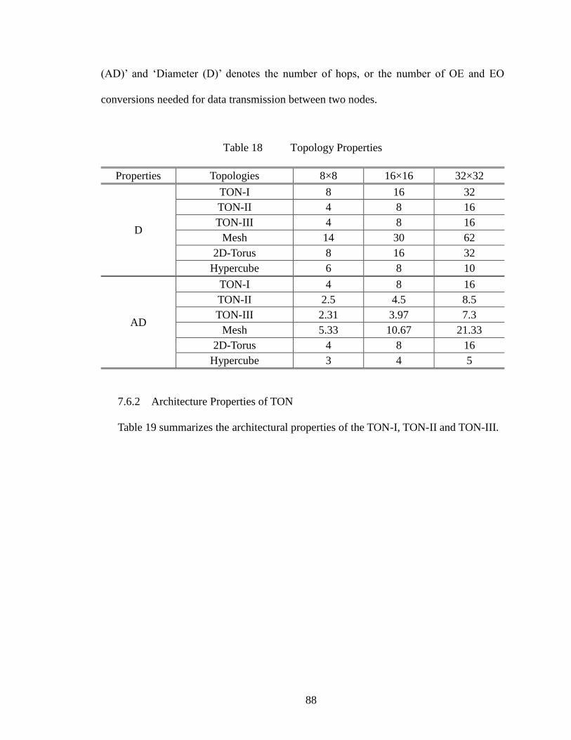
88
(AD)‟ and „Diameter (D)‟ denotes the number of hops, or the number of OE and EO
conversions needed for data transmission between two nodes.
Table 18 Topology Properties
Properties Topologies 8×8 16×16 32×32
D
TON-I 8 16 32
TON-II 4 8 16
TON-III 4 8 16
Mesh 14 30 62
2D-Torus 8 16 32
Hypercube 6 8 10
AD
TON-I 4 8 16
TON-II 2.5 4.5 8.5
TON-III 2.31 3.97 7.3
Mesh 5.33 10.67 21.33
2D-Torus 4 8 16
Hypercube 3 4 5
7.6.2 Architecture Properties of TON
Table 19 summarizes the architectural properties of the TON-I, TON-II and TON-III.

89
Table 19 Architecture Properties of TON-1
Architecture Properties TON-I TON-II TON-III
Channels per node 4 8 10
Lasers per node 4 8 10
Photodetectors per node 4 8 10
Routing wavelengths per node 2 4 5
Total routing wavelengths in the network 2 4 6
MRRs per node 4 8 12
MRR optical switches per node 2 4 6
Electrical input queues per node 4 8 10
Electrical output queues per node 0 0 0
Optical buffers per node 0 0 0
Optical couplers per node 2 2 2
Electrical crossbar switches per node 1 1 1
Wavelength multiplexers per node 1 1 1
Wavelength demultiplexers per node 1 1 1
TO/EO tuning devices in the network 0 0 0
7.7 Routing Algorithms of TON Architectures
The Johnson code is used in TON for node addressing and data routing.
7.7.1 Johnson Code Addressing for TON
To implement the data routing in the network the Johnson Code explained in Section
6.3 is applied for node addresses in TON.
7.7.1.1 Addressing Nodes in TON
The address of a node (Ah, Av) in the NN TON can be defined by means of two n-bit
Johnson Codes (Ch, Cv) where N=2n.
For example, (3, 2) in a 66 GTON is addressed as 011001.
7.7.1.2 Nodes Coordinates and Address Association
For a node address C = Ch|Cv, C is of N bits and N = 4n, Ch and Cv are both 2n bits

90
where
h
n
h
j
h
j
h
j
hh
h bbbbbbC 21121 (31)
v
n
v
j
v
j
v
j
vv
v bbbbbbC 21121 (32)
Then the node‟s coordinates (Ah, Av) can be derived from Ah = fa (Ch) and Av = fa (Cv)
where
12
0
1
2
1
1
2
1
bifbn
bifbCf
n
ii
n
ii
a (33)
7.7.2 Routing Functions in TON
7.7.2.1 Routing Direction Function fr
In the routing algorithm, the most important function is fr which can be used to
determine the direction of routing, in another word, to choose the next routing channel.
Actually, fr is the function to determine the position relationship between two shift-codes.
Given two m bits Johnson-codes: S and D where
S = s1s2s3…sm
D = d1d2d3…dm
The function fr is (p,c) = fr(S,D) where
m
iii dscp
1
(34)
And c is calculated as following:
If s1 = d1 = 0, then
m
ii
m
ii
m
ii
m
ii
sdif
sdifc
11
11
1
1 (35)

91
elseif s1 = d1 = 1, then
m
ii
m
ii
m
ii
m
ii
sdif
sdifc
11
11
1
1 (36)
elseif s1 = 0, d1 = 1, then
m
ii
m
ii
m
ii
m
ii
sdif
sdifc
11
11
1
1 (37)
elseif s1 = 1, d1 = 0, then
m
ii
m
ii
m
ii
m
ii
sdif
sdifc
11
11
1
1 (38)
7.7.2.2 Routing Address Function fd
The Routing Address Function fd is to calculate the node address from the current
node address with an offset value.
Given the shift code Cc and offset value O, where
c
n
c
j
c
j
c
j
cc
c bbbbbbC 1121
The new shift code iC can be derived by
in
i
j
i
j
i
j
ii
cdi bbbbbbOCfC 1121, (39)
where
120
211
0
nji
njin
nji
b i
j (40)
and
OAi (41)
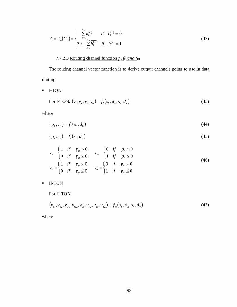
92
12
0
1
2
1
1
2
1
cn
k
c
k
cn
k
c
k
ca
bifbn
bifbCfA (42)
7.7.2.3 Routing channel function fI, fII and fIII
The routing channel vector function is to derive output channels going to use in data
routing.
I-TON
For I-TON, vvhhInswe dsdsfvvvv ,,,,,, (43)
where
hhrhh dsfcp ,, (44)
vvrvv dsfcp ,, (45)
01
00
00
01
01
00
00
01
v
v
n
v
v
s
h
h
w
h
h
e
pif
pifv
pif
pifv
pif
pifv
pif
pifv
(46)
II-TON
For II-TON,
vvhhIInnsswwee dsdsfvvvvvvvv ,,,,,,,,,, 21212121 (47)
where

93
00
02
00
02
00
02
00
02
00
02
00
02
00
02
00
02
2
12
2
12
2
12
2
12
v
vn
n
v
vv
n
v
vsv
s
v
vv
s
h
hwh
w
h
hh
w
h
heh
e
h
hh
e
pif
pifmpvm
pif
pifp
m
pif
pifmpm
pif
pifp
m
pif
pifmpm
pif
pifp
m
pif
pifmpm
pif
pifp
m
(48)
and
00
01
00
01
00
01
00
01
00
01
00
01
00
01
00
01
2
2
2
1
1
1
2
2
2
1
1
1
2
2
2
1
1
1
2
2
2
1
1
1
n
n
e
n
n
n
s
s
s
s
s
s
w
w
w
w
w
w
e
e
e
e
e
e
mif
mifv
mif
mifv
mif
mifv
mif
mifv
mif
mifv
mif
mifv
mif
mifv
mif
mifv
(49)
III-TON
For III-TON,
*
2
*
1
*
2
*
1
*
2
*
1
*
2
*
1
21212121
,,,,,,,*
,,,,,,,,,
,,,*,
nnsswwee
nwsennsswwee
vvhhIII
vvvvvvvvW
vvvvvvvvvvW
dsdsfWW
(50)

94
00
02
00
02
00
02
00
02
00
02
00
02
00
02
00
02
2
12
2
12
2
12
2
12
v
vn
n
v
vv
n
v
vsv
s
v
vv
s
h
hwh
w
h
hh
w
h
heh
e
h
hh
e
pif
pifmpvm
pif
pifp
m
pif
pifmpm
pif
pifp
m
pif
pifmpm
pif
pifp
m
pif
pifmpm
pif
pifp
m
(51)
00
01
00
01
00
01
00
01
00
01
00
01
00
01
00
01
2
2*
2
1
1*
1
2
2*
2
1
1*
1
2
2*
2
1
1*
1
2
2*
2
1
1*
1
n
n
n
n
n
n
s
s
s
s
s
s
w
w
w
w
w
w
e
e
e
e
e
e
mif
mifv
mif
mifv
mif
mifv
mif
mifv
mif
mifv
mif
mifv
mif
mifv
mif
mifv
(52)
Update {m} with the algorithm as shown in Figure 40.

95
Figure 40 Algorithm to update {m}.
Then
00
01
00
01
00
01
00
01
00
01
00
01
00
01
00
01
00
01
00
01
2
2
2
1
1
1
2
2
2
1
1
1
2
2
2
1
1
1
2
2
2
1
1
1
nw
nw
nw
se
se
se
n
n
e
n
n
n
s
s
s
s
s
s
w
w
w
w
w
w
e
e
e
e
e
e
mif
mifv
mif
mifv
mif
mifv
mif
mifv
mif
mifv
mif
mifv
mif
mifv
mif
mifv
mif
mifv
mif
mifv
(53)
7.7.2.4 Routing vector function fv1, fv2 and fv3
I-TON
For I-TON, vvhhv dsdsfV ,,,1 where the routing vector V is generate with the
Start:
mnw = 0, mse = 0
While mw1>1 & mn2>1
mw1 = mw1-1, mn2 = mn2-1
mnw = mnw+1, me1 = me1+1
End
While mn1>1 & mw2>1
mw1 = mn1-1, mn2 = mw2-1
mnw = mnw+1, ms1 = ms1+1
End
While ms1>1 & me2>1
ms1 = ms1-1, me2 = me2-1
mse = mse+1, mn1 = mn1+1
End
While me1>1 & ms2>1
Me1 = me1-1, ms2 = ms2-1
mse = mse+1, mw1 = mw1+1
End
End

96
algorithm as shown in Figure 41.
Figure 41 Algorithm to generate the routing vector V for TON-I.
II-TON
For II-TON, vvhhv dsdsfV ,,,2 where the routing vector V is generate with the
algorithm as shown in Figure 42.
Start:
Initialize V = ф
While ve>0
V = V+E, ve = ve-1
End
While vw>0
V = V+W, vw = vw-1
End
While vs>0
V = V+S, vs = vs-1
End
While vn>0
V = V+N, vn = vn-1
End
End

97
Figure 42 Algorithm to generate the routing vector V for TON-II.
III-TON
For III-TON, vvhhv dsdsfV ,,,3 where the routing vector V is generate with the
algorithm as shown in Figure 43.
Start:
,
Initialize V = ф
While ve2>0
V = V+E2, ve2 = ve2-1
End
While ve1>0
V = V+E1, ve1 = ve1-1
End
While vw2>0
V = V+W2, vw2 = vw2-1
End
While vw1>0
V = V+W1, vw1 = vw1-1
End
While vs2>0
V = V+S2, vs2 = vs2-1
End
While vs1>0
V = V+S1, vs1 = vs1-1
End
While vn2>0
V = V+N2, vn2 = vn2-1
End
While vn1>0
V = V+N1, vn1 = vn1-1
End
End

98
Figure 43 Algorithm to generate the routing vector V for TON-III.
7.7.3 Relationship between Nodes Coordinates and Address
Given a node address in the TON is C = Ch|Cv (C is N bits where N = 4n, Ch and Cv
are both 2n bits) where
h
n
h
j
h
j
h
j
hh
h bbbbbbC 21121 (54)
v
n
v
j
v
j
v
j
vv
v bbbbbbC 21121 (55)
Start:
Initialize V = φ
While ve2>0
V = V+E2, ve2 = ve2-1
End
While ve1>0
V = V+E1, ve1 = ve1-1
End
While vw2>0
V = V+W2, vw2 = vw2-1
End
While vw1>0
V = V+W1, vw1 = vw1-1
End
While vs2>0
V = V+S2, vs2 = vs2-1
End
While vs1>0
V = V+S1, vs1 = vs1-1
End
While vn2>0
V = V+N2, vn2 = vn2-1
End
While vn1>0
V = V+N1, vn1 = vn1-1
End
End

99
Then the node‟s coordinates vh AA , can be derived by the function hah CfA and
vav CfA where
12
0
1
2
1
1
2
1
bifbn
bifbCf
n
ii
n
ii
a (56)
7.7.4 Deterministic Routing Algorithm for TONs
We classified all channels in TONs to three classes: X-channel, Y-channel and Z-
channel. In I-TON, channel E and W are X-channels, channel N and S are Y-channels. In
II-TON and III-TON, channel E1, E2, W1 and W2 are X-channels, channel N1, N2, S1
and S2 are Y-channels. And channel SE and NW are Z-channels.
In deterministic routing, all data transmission should follow X-Y sequence in I-TON
and II-TON, and Z-X-Y sequence in III-TON.
There are two types of deterministic routing algorithms for each TON, dynamic
routing and predetermined routing. In dynamic routing,
7.7.4.1 Dynamic routing
In dynamic routing, the routing is implemented in each mid node. Before the data
package arrive to its destination node, in each intermediary node, the router will read its
header to find its destination address, and then based on the destination node address D
and the current node address S, one channel will be selected and the data package will be
transmitted along this channel.
Dynamic routing algorithm I-TON
The dynamic routing algorithm of I-TON is shown in Figure 44.

100
Figure 44 Dynamic routing algorithm of I-TON.
Dynamic routing algorithm for II-TON
The dynamic routing algorithm of II-TON is shown in Figure 45.
Algorithm Routing (S→D):
Begin:
Compare D and the Current Address S
If &
channel = internal
Elseif
channel = E
Elseif
channel = W
Elseif &
channel = S
Elseif &
channel = N
End
End Routing

101
Figure 45 Dynamic routing algorithm of II-TON.
Dynamic routing algorithm for III-TON
In routing within III-TON, we have following equal routing channel combinations.
SEWSE
SENSE
NWSNW
NWENW
121
112
112
121
(57)
To maximize the utilization of all channels and network throughput, Z-channels has
the highest priorities in channel assignment.
The dynamic routing algorithm of III-TON is shown in Figure 46.
Algorithm Binary (S→D):
Begin:
Compare D and the Current Address S
If ph = 0 & pv = 0
channel = internal
Elseif ph ≥ 2
channel = E2
Elseif 0 < ph < 2
channel = E1
Elseif ph ≤ -2
channel = W2
Elseif 0 > ph > -2
channel = W1
Elseif pv ≥ 2
channel = S2
Elseif 0 < pv < 2
channel = S1
Elseif pv ≤ -2
channel = N2
Elseif 0 > pv > -2
channel = N1
End
End Routing

102
Figure 46 Dynamic routing algorithm of III-TON.
7.7.4.2 Predetermined routing
In predetermined routing, before a data package is sent from its source node, all its
Algorithm Binary (S→D):
Begin:
Compare D and the Current Address S
If ph = 0 & pv = 0
channel = internal
Elseif ph ≥ 2
If pv ≥ 1
channel = SE
Else
channel = E2
Elseif 0 < ph < 2
If pv ≥ 2
channel = channel SE
Else
channel = channel E
Elseif ph ≤ -2
If pv ≤ -1
channel = NW
Else
channel = W2
Elseif 0 > ph > -2
If pv ≤ -2
channel = NW
Else
channel = W
Elseif pv ≥ 2
channel = channel S2
Elseif 0 < pv < 2
channel = channel S1
Elseif pv ≤ -2
channel = channel N2
Elseif 0 > pv > -2
channel = channel N1
End
End Routing

103
routing path is determined and stored as a routing channel vector V in the header. The
routing vector is composed of a sequence of channels going to use in the routing. In each
intermediary node, the router will read the header, assign the output channel according to
the first element in the routing vector, then update V to remove the used element and
replace V into the header.
Predetermined routing algorithm I-TON
The predetermined routing algorithm of I-TON is shown in Figure 47.
Figure 47 Predetermined routing algorithm of I-TON.
Predetermined routing algorithm II-TON
The predetermined routing algorithm of II-TON is shown in Figure 48.
Algorithm Routing (S→D):
Generate the routing vector V:
Routing:
While V ≠ ф
vl = the first element in V
channel = vl
Update V by removing vl from V
End

104
Figure 48 Predetermined routing algorithm of II-TON.
Predetermined routing algorithm III-TON
The predetermined routing algorithm of II-TON is shown in Figure 49.
Figure 49 Predetermined routing algorithm of III-TON.
7.7.5 Basic Adaptive Routing Algorithm for TONs
In basic adaptive routing, the routing paths from source node to destination node are
vary depends on the traffic condition but all their lengths are maintained to be same to the
minimum.
Here a new function Tc is introduced to describe the traffic condition in a node which
will be used in output channel decision-making in adaptive routing.
Algorithm Routing (S→D):
Generate the routing vector V:
Routing:
While V ≠ ф
vl = the first element in V
channel = vl
Update V by removing vl from V
End
Algorithm Routing (S→D):
Generate the routing vector V:
Routing:
While V ≠ ф
vl = the first element in V
channel = vl
Update V by removing vl from V
End
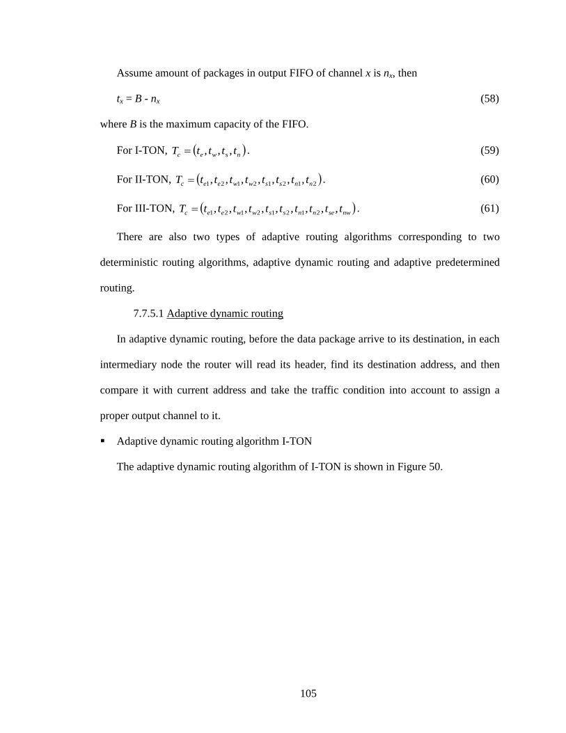
105
Assume amount of packages in output FIFO of channel x is nx, then
tx = B - nx (58)
where B is the maximum capacity of the FIFO.
For I-TON, nswec ttttT ,,, . (59)
For II-TON, 21212121 ,,,,,,, nnsswweec ttttttttT . (60)
For III-TON, nwsennsswweec ttttttttttT ,,,,,,,,, 21212121 . (61)
There are also two types of adaptive routing algorithms corresponding to two
deterministic routing algorithms, adaptive dynamic routing and adaptive predetermined
routing.
7.7.5.1 Adaptive dynamic routing
In adaptive dynamic routing, before the data package arrive to its destination, in each
intermediary node the router will read its header, find its destination address, and then
compare it with current address and take the traffic condition into account to assign a
proper output channel to it.
Adaptive dynamic routing algorithm I-TON
The adaptive dynamic routing algorithm of I-TON is shown in Figure 50.

106
Figure 50 Adaptive dynamic routing algorithm of I-TON.
Adaptive dynamic routing algorithm II-TON
The adaptive dynamic routing algorithm of II-TON is shown in Figure 50.
Figure 51 Adaptive dynamic routing algorithm of II-TON.
Adaptive dynamic routing algorithm III-TON
The adaptive dynamic routing algorithm of III-TON is shown in Figure 52.
Algorithm Routing (S→D):
Begin:
*
channel = c
End
* The operator „ ‟ in the algorithm represents
the element-by-element product of the two
arrays.
Algorithm Routing (S→D):
Begin:
channel = c
End

107
Figure 52 Adaptive dynamic routing algorithm of III-TON.
7.7.5.2 Adaptive predetermined routing
In adaptive predetermined routing, the sequence of routing channels in the routing
vector V should be modified according the real-time traffic condition to minimize the
latency in each intermediate node.
Adaptive predetermined routing algorithm I-TON
The adaptive predetermined routing algorithm of I-TON is shown in Figure 53.
Figure 53 Adaptive dynamic routing algorithm of I-TON.
Adaptive predetermined routing algorithm for II-TON
The adaptive predetermined routing algorithm of II-TON is shown in Figure 54.
Algorithm Routing (S→D):
Begin:
channel = c
End
Algorithm Routing (S→D):
Generate the routing channels:
Routing:
While WI ≠ 0
SI =(si|si = sign (vi, vi WI)
v = max{vi|vi (S Tc)}
channel = v
Update WI by reducing 1 from the channel of v from WI.
End

108
Figure 54 Adaptive dynamic routing algorithm of II-TON.
Adaptive predetermined routing Algorithm for III-TON
The adaptive predetermined routing algorithm of III-TON is shown in Figure 55.
Figure 55 Adaptive dynamic routing algorithm of III-TON.
It can be seen that the algorithm is not optimal because it does not include channel
substitute between horizontal/vertical channels and diagonal channels, to match the
fastest output channel. The reason is that such substitute will need the update of routing
vector WI in each intermediate node, which is almost same to adaptive dynamic routing
Algorithm Routing (S→D):
Generate the routing channels:
Routing:
While WI ≠ 0
sign
channel = v
Update WI by reducing 1 from the channel of v from WI.
End
Algorithm Routing (S→D):
Generate the routing channels
Routing:
While WI ≠ 0
sign
channel = v
Update WI by reducing 1 from the channel of v from WI.
End

109
algorithm.
7.8 Simulation and Analysis
7.8.1 Simulation Setup
We test the maximum traffic load the network can handle without blocking. The
network is set to be homogeneous; and all nodes have the same frame generating rate.
Simulation parameters are listed in Table 20.
Table 20 Simulation Setting
Optical Frequency 40G
Electrical Frequency 4G
Frame Length 256 bits
Electrical Bus Width 128 bits
Frame Generating Rate 2.410-3
~ 0.08 frame/nanosecond
Frame Generation Uniform Distribution
Network Size 66 ~ 1616
Routing Algorithm Deterministic Routing
Buffer service FIFO
At least 10,000 frames are generated by each node per simulation run and transmitted
to other nodes with the same probability. Frames generated by a core are switched to an
output channel via a crossbar. Data are modulated to a sequence of serial optical data bits
and transmitted to the next node through a waveguide. On the receiving side, the optical
bit sequence is received by a photodetector and converted to a parallel electrical data
frame. This process repeats until the frame arrives to its destination core. The total time
of the process is the frame transmission time.
We consider first a deterministic routing algorithm, in which data are transmitted
according to the following sequence: Level3 channels first, Level2 channels second and

110
Level1 channels last. In Level1 channels x-y routing is applied to avoid the deadlock.
7.8.2 Simulation Results for TON-I
An average frame transmission time in TON-I networks of different sizes and with
different frame generating rates are shown in Figure 56. It can be observed that before a
point when the network reaches the blocking condition the waiting time is negligible.
Figure 56 Average frame transmission time in TON-I
As it was mentioned before, each channel has an input buffer. An average and a
maximum utilization of these buffers are shown in Figure 57 and Figure 58.

111
Figure 57 Average input buffer utilization in TON-I
Figure 58 Maximum input buffer utilization in TON-I

112
7.8.3 Simulation Results for TON-II
An average frame transmission time in TON-II of different sizes and with different
frame generating rates are shown in Figure 59. It can be observed that before a point
when the network reaches the blocking condition the waiting time is negligible.
Figure 59 Average frame transmission time in TON-II
The average and maximum utilization of input buffers are shown in Figure 60 and
Figure 61.

113
Figure 60 Average input buffer utilization in TON-II
Figure 61 Maximum input buffer utilization in TON-II

114
7.8.4 Simulation Results for TON-III
An average frame transmission time in networks of different sizes and with different
frame generating rates are shown in Figure 62. It can be observed that before a point
when the network reaches the blocking condition the waiting time is negligible.
As it was mentioned before, each channel is equipped with an input buffer. An
average and a maximum utilization of these buffers are shown in Figure 63 and Figure 64.
From simulation results shown in Figure 56 to Figure 64, it can be seen that with a
number of DOCs increasing from 4 to 8 and 10, as in TON-I, II and III, respectively, the
average single frame transmission time from the source node to the destination node and
an average/maximum buffer usage are dropped remarkably; the buffer usage becomes
aligned.
Figure 62 Average frame transmission time in TON-III

115
Figure 63 Average input buffer utilization in TON-III
Figure 64 Maximum input buffer utilization in TON-III

116
TON architectures are highly scalable due to packet-switching. The frame
transmission time in TON architectures mainly depends on the number of hops or EO/OE
conversion and the transmission time in each channel. The architectures utilize passive
MRRs for signal switching and wavelength-multiplexing can be used in each optical
channel to provide multiple simultaneous communications. Hence overall network
throughput is expected to be extremely high. Direct optical channels (DOCs) offer
various shortcuts and their combination significantly reduce distances between remote
node pairs in the network. Due to the availability of multiple routing paths between node
pairs, the communication in TON networks is highly fault tolerant.
7.9 Power Analysis
7.9.1 Electrical Back-end Components
Table 21 shows the estimated energy costs of the electrical back-end for the optical
link (drivers, receivers, and clocking) using a predictive technology model for the 22nm
node [62]. The dominant source of energy consumption is the modulator driver, followed
by the optical receiver and clocking circuits. Based on these parameters Tab.15 can be
derived which listed energy consumed for transmitting a single bit via single DOC in
TON-I, II and III, respectively. Then the average energy consumption for transmitting a
single bit between any two cores in TON-I, II and III are shown in Table 22 respectively.

117
Table 21 Estimated energy of optical components
Component Energy (fJ/b)
Serializer 1.5
Pre-Driver 19.0
Push-Pull Modulater 70.0
Analog Receiver Front End 40.0
Flip-Flop Sampling & Monitoring 12.0
Deserializer 1.5
Optical Clocking Source 2.0
Clock Phase Control 12.0
Laser 300.0
Total 458
Table 22 Estimated energy consumption of single channel in TON-I, II, and III
Architecture TON-I TON-II TON-III
Electrical Energy (fJ/b) per Channel 5.715 7.695 8.880
Optical Energy (fJ/b) per Channel 458 458 458
Total Energy (fJ/b) per Channel 463.715 465.695 466.88
Table 23 Estimated energy consumption of single channel in TON-I, II and III
Energy Topologies 8×8 16×16 32×32
AD
TON-I 1854.86 3709.72 7419.44
TON-II 1164.24 2095.63 3958.41
TON-III 1078.49 1853.51 3408.22
7.9.2 Transmission Power Loss
The optical power loss of the MRR switch matrix mainly is due to off-state, on-state
losses, waveguide crossing loss and waveguide propagation loss [23].
In our analysis, the waveguide propagation loss is neglected. Other loss values are
adopted according to [60], as shown in Table 24. Transmission power losses in each
channel in TON-I, II and III are listed in Table 25, Table 26 and 0, respectively.

118
Table 24 Optical Power Budget
Component Loss(dB)
MRR off-state 0.06
MRR on-state 1.5
Waveguide Crossing 0.05
Table 25 Transmission Power Loss in TON-I
Port Wavelength Channel Power Loss (dB)
LS w1 E1 1.67
w2 S1 1.67
LD w1 W1 1.67
w2 N1 1.67
Table 26 Transmission Power Loss in TON-II
Node Channel Wavelength Port Power Loss (dB)
I-Node
E1 w1
LS
2.00
E2 w2 2.22
S2 w3 3.56
S1 w4 2.00
W1 w1
LD
2.00
W2 w2 2.22
N2 w3 3.56
N1 w4 2.00
II-Node
E1 w1
LS
2.00
S2 w2 3.56
E2 w3 3.77
S1 w4 2.00
W1 w1
LD
2.00
N2 w2 3.56
W2 w3 3.77
N1 w4 2.00

119
Table 27 Transmission Power Loss in TON-III
Node Channel Wavelength Port Power Loss (dB)
I-Node
E1 w1
LS
2.22
S2 w3 3.80
SE w4 5.78
E2 w5 5.34
S1 w6 2.02
W1 w1
LD
2.12
N2 w3 3.8
NW w4 5.78
W2 w5 3.9
N1 W6 2.23
II-Node
E1 w1
LS
2.12
SE w2 4.68
E2 w3 2.44
S2 w5 3.90
S1 w6 2.22
W1 w1
LD
2.22
NW w2 4.68
W2 w3 2.44
N2 w5 3.90
N1 w6 2.02
It can be seen from Table 25 to 0, transmission losses in TON-I, II and III is around
1.67dB, 2.64dB and 3.38dB, with maximum 1.67dB, 3.77dB and 5.78dB, respectively.
The channel transmission loss is linear to the channel length, or the number of OIUs
in the channel. Losses in each OIU are related to the number of MRR switches in it,
which is linear to the number of DOCs in each node.
In most ONoC architectures which use MRR tuning, optical receivers have to deal
with a wide power range because the transmission power loss depends on the specific
path. Wide power range receivers are difficult to implement. On the contrary, in TONs,
the transmission power loss per DOC is a constant, and thus the receiver is less complex.
120
7.10 Conclusion
In this chapter three different 2D-torus based packet switching optical NoC
architectures TON-I, TON-II and TON-III are proposed. These packet-switching TONs
architectures are highly scalable. The use of passive MRR switching, WDM and direct
optical channels (DOCs) offers an extremely high bandwidth, low latency, low cost, low
power consumption, and fault tolerance property. The performances of the TON networks
are evaluated by simulation and the results demonstrate that the TONs have high
throughputs. TON-I has a lesser cost and hence a relatively lower network performance,
whereas TON-III has a highest performance but requires complex hardware and control.
TON-II represents a good tradeoff between these three architectures. Related issues such
as communication energy and transmission power losses are also addressed. Many
outstanding features of the designed TON architectures make it to be a compelling
solutions for future optical NoCs.

121
CHAPTER 8
GENERALIZED PACKET SWITCHING OPTICAL NETWORK-ON-CHIP
ARCHITECTURES
In this chapter a Generalized 2D-Torus-based Optical Network-on-Chip (GTON) is
proposed. GTON is a generalized packet switching optical NoC architecture based on
micro-ring resonator (MRR) optical switches. Given sufficient routing wavelengths, any
network topology can be implemented in GTON. A systematic approach of the design of
network interconnections and routers in GTON is presented explicitly. The use of passive
MRR switching, Wavelength Division Multiplexing (WDM) and Direct Optical Channels
(DOC) allows for attaining high bandwidth and makes GTON fault tolerant. The GTON
architecture requires a small number of routing wavelengths and MRRs and demonstrates
low cost, latency and power consumption. The performance of the network is evaluated
by simulation. Related issues such as channel design, transmission power loss and the
buffer analysis are provided.
8.1 Introduction
The physical interconnection in GTON is same to 2D-torus. The new concept of
direct optical channel (DOC) is adopted in GTON to identify a direct light path between
two nodes. A DOC is a set of interconnected physical links (waveguides). By using a
predetermined routing wavelength, light travels in a DOC without relay. Optical data
packets are switched between DOCs in the GTON. Theoretically, the DOC can be
introduced to connect any two nodes in the network and thus any existing network
topology can be built on the GTON [84].

122
8.2 GTON Architecture Overview
The GTON is an NN, where N=2n, nN, 2D-torus-based network. A 66 GTON
example is presented in Figure 65. Each node in the GTON is presented by a pair (x,y)
where x,y={0,1,…,N-1}. Each node has a router and a processor (core), and it is
physically connected to four adjacent nodes. Internally, each router has a wavelength
routed Optical Interconnection Unit (OIU) and an Optical Electrical Router (OER). OIU
is a MRR matrix device with six ports, of which four are external ports (S1, S2, D1, D2),
and two, i.e., (LS, LD) are internal ports to connect to the OER.
The GTON nodes are classified into two classes: I-Node associated with I-router; and
II-node with II-router. I-router has an I-OIU and an I-OER, and II-router has an II-IOU
and an II-OER. Given coordinates (x, y), a node is an I-Node if x + y = 2n (nN),
otherwise it is a II-Node.
Router
I-OIU
I-OER
CORE
Router
II-OIU
II-OER
CORE
I-Node II-Node I-Node II-Node I-Node II-Node
(3,0)(0,0) (1,0) (2,0) (5,0)(4,0)
(3,1)(0,1) (1,1) (2,1) (5,1)(4,1)
I-Node II-Node I-Node II-Node I-NodeII-Node
(3,2)(0,2) (1,2) (2,2) (5,2)(4,2)
I-Node II-Node I-Node II-Node I-Node II-Node
(3,3)(0,3) (1,3) (2,3) (5,3)(4,3)
I-Node II-Node I-Node II-Node I-NodeII-Node
(3,4)(0,4) (1,4) (2,4) (5,4)(4,4)
I-Node II-Node I-Node II-Node I-Node II-Node
(3,5)(0,5) (1,5) (2,5) (5,5)(4,5)
I-Node II-Node I-Node II-Node I-NodeII-Node
Figure 65 6×6 GTON network topology

123
The interconnection of the 66 GTON is shown in Figure 65. It can be seen that for
the I-Node at (x, y), its S1 port is connected to the S2 port of the II-node at (x, y-1), S2
port is connected to the D2 of the II-node at (x-1, y), D1 is connected to the S1 of the II-
node at (x+1, y), and D2 is connected to the D1 of the II-node at (x, y+1). And for the II-
Node at (x, y), its S1 port is connected to the D1 port of the I-node at (x-1, y), S2 is
connected to the S1 of the I-node at (x, y+1), D1 is connected to the D2 of the I-node at (x,
y-1), and D2 is connected to the S2 of the I-node at (x+1, y).
I-OIU
I-OER
CORE
II-OIU
II-OER
CORE
II-OIU
II-OER
CORE
I-OIU
I-OER
CORE
I-OIU
I-OER
CORE
I-OIU
I-OER
CORE
I-OIU
I-OER
CORE
I-OIU
I-OER
CORE
I-OIU
I-OER
CORE
I-OIU
I-OER
CORE
II-OIU
II-OER
CORE
II-OIU
II-OER
CORE
(0,0)
LS LD
S1
S2
D1
D2
II-OIU
II-OER
CORE
II-OIU
II-OER
CORE
II-OIU
II-OER
CORE
II-OIU
II-OER
CORE
(1,0)
LS LD
S1
S2
D1
D2
(2,0)
LS LD
S1
S2
D1
D2
(3,0)
LS LD
S1
S2
D1
D2(0,1)
LSLD
S1
S2
D1
D2
(1,1)
LS LD
S1
S2
D1
D2
(2,1)
LSLD
S1
S2
D1
D2
(3,1)
LS LD
S1
S2
D1
D2(1,2)
LSLD
S1
S2
D1
D2
(0,2)
LS LD
S1
S2
D1
D2
(2,2)
LS LD
S1
S2
D1
D2
(3,2)
LS LD
S1
S2
D1
D2(0,3)
LS LD
S1
S2
D1
D2
(1,3)
LS LD
S1
S2
D1
D2
(2,3)
LSLD
S1
S2
D1
D2
(3,3)
LS LD
S1
S2
D1
D2
I-OIU
I-OER
CORE
I-OIU
I-OER
CORE
I-OIU
I-OER
CORE
I-OIU
I-OER
CORE
II-OIU
II-OER
CORE
II-OIU
II-OER
CORE
II-OIU
II-OER
CORE
II-OIU
II-OER
CORE
(4,0)
LS LD
S1
S2
D1
D2
(5,0)
LS LD
S1
S2
D1
D2(4,1)
LSLD
S1
S2
D1
D2
(5,1)
LS LD
S1
S2
D1
D2(4,2)
LS LD
S1
S2
D1
D2
(5,2)
LS LD
S1
S2
D1
D2(4,3)
LSLD
S1
S2
D1
D2
(5,3)
LS LD
S1
S2
D1
D2
I-OIU
I-OER
CORE
I-OIU
I-OER
CORE
I-OIU
I-OER
CORE
I-OIU
I-OER
CORE
II-OIU
II-OER
CORE
II-OIU
II-OER
CORE
II-OIU
II-OER
CORE
II-OIU
II-OER
CORE
(1,4)
LSLD
S1
S2
D1
D2
(0,4)
LS LD
S1
S2
D1
D2
(2,4)
LS LD
S1
S2
D1
D2
(3,4)
LS LD
S1
S2
D1
D2(0,5)
LS LD
S1
S2
D1
D2
(1,5)
LS LD
S1
S2
D1
D2
(2,5)
LSLD
S1
S2
D1
D2
(3,5)
LS LD
S1
S2
D1
D2
I-OIU
I-OER
CORE
I-OIU
I-OER
CORE
II-OIU
II-OER
CORE
II-OIU
II-OER
CORE
(4,4)
LS LD
S1
S2
D1
D2
(5,4)
LS LD
S1
S2
D1
D2(4,5)
LSLD
S1
S2
D1
D2
(5,5)
LS LD
S1
S2
D1
D2
: 2-hop DOC: 1-hop DOC
Figure 66 A 6×6 GTON architecture and examples of DOCs.

124
Unlike other optical architectures, data transmission in GTON is via a DOC. The
DOC is a light path between two nodes that consists of one or more physical links and
OIUs. By utilizing a predetermined routing wavelength and with properly designed OIUs
light can travel through the DOC without any relay or arbitration. DOCs can be placed
between any two nodes. Examples of a one-hop DOC and a two-hop DOC in the 66
GTON are shown in Figure 65.
Two nodes which do not have a DOC, data packets are transmitted by relaying in
intermediary nodes. This would require electrical/optical and optical/electrical (E/O &
O/E) conversion. Data transmission latency is directly related to the number of such
conversions.
8.3 GTON Design Schema
In this section we introduce the design of a GTON architecture given a target
topology. As it has been mentioned earlier, the GTON is a generalized architecture. Any
topology which uses 2D-coordinate addressing can be mapped into the GTON. A key
issue here is to design the router, i.e. OIU and OER for each node to realize DOCs
required by the network topology. The design procedure includes the following steps:
1. Convert the target network topology into channel map.
2. Map channels into DOCs.
3. Derive wavelength routing table per OIU, and assign wavelengths to DOCs.
4. Design OIUs based on wavelength routing table.
5. Design OERs based on the wavelength table and the OIUs design.
The design of a special network architecture called GTON-XII is illustrated in the
next subsection.

125
8.3.1 GTON-XII Topology
GTON-XII topology is 2D-torus based. Each node in the network is directly
connected to 12 other nodes via 12 DOCs. Given a node (x, y), its channel map is shown
in Figure 67. The twelve DOCs are:
E1: (x, y) (x +1, y); W1: (x, y) (x-1, y); S1(x, y) (x, y+1); N1: (x, y) (x,
y-1); E2: (x, y) (x+2, y); W2: (x, y) (x-2, y), S2: (x, y) (x, y+2); N2: (x, y) (x,
y-2); SE: (x, y) (x+2, y+2); NW: (x, y) (x-2, y-2), NE: (x, y) (x+2, y-2); and SW:
(x, y) (x-2, y+2).
These DOC are grouped into three levels: Level 1 with channels E1, W1, S1 and N1,
which are one-hop connections in X or Y direction; Level 2 with channels E2, W2, S2
and N2, which are two-hop connections in X or Y direction; and Level 3 with channels
NE, NW, SE and SW, which are two-hop diagonal connections.
The minimum size of GTON-XII is 66 to avoid multiple DOCs between the same
pair of nodes.

126
Figure 67 Node channel map in GTON-XII
8.3.2 Network Properties of GTON-XII
The GTON-XII network has the following properties.
Lemma 10. The diameter D of an NN GTON-XII is
14
ND (62)
Lemma 11. The average distance AD between any pair of nodes in the GTON-XII
can be derived from the following equations.
If N = 4m, then
348
36322
23
m
mmmAD (63)
Else when N+2 =4m, then
94848
31112322
23
mm
mmmAD (64)
Table 28 compares the network properties of GTON and a few other popular

127
networks. „Average Distance‟ denotes the number of hops, or the number of OE and EO
conversions needed for data transmission between two nodes.
Table 28 Diameter (D) and Average Distance (AD) for Different Networks.
Network
Size
GTON-XII Mesh 2D-Torus Hypercube
D AD D AD D DS D AD
8×8 3 2.13 14 5.33 8 4 6 3
16×16 5 3.44 30 10.67 16 8 8 4
32×32 9 6.09 62 21.33 32 16 10 5
8.3.3 Channel Mapping in GTON-XII
Mapping of the 12 channels into DOCs means selection of a direct light path for each
channel. Since there are always more than one solutions available for each channel, we
enforce the following rules in such selection to minimize the cost of the resulted DOC:
1. For each DOC, the internal routing path for the same type routers must be the same,
which means that if one I-router in the DOC uses the internal routing path from port
S1 to D1 (S1D1), then all other I-routers in this DOC must also use the internal
routing path as S1D1.
2. Among different DOCs, using as less as possible different internal paths for the router
of a same type such that the number of required wavelengths is minimal.
Based on these rules one solution of mapping of 12 channels in GTON-XII is
presented in Table 30 - 0. Table 29 - 0 are for I-node and Table 32 - 0 are for II-node. In
these tables, each line represents a DOC. The channeling column shows physical path of
the optical signal.
For example, in the first row in Table 30, „(x,y)LS(x,y)D1(x+1,y)S1(x+1,y)LD‟

128
indicates routing the signal from LS to D1 in node (x, y), which is an internal path; then
transmission from D1 port of node (x,y) to S1 port of node (x+1,y), which is an external
path. In (x+1, y) nodes it is routed from S1 to LD, which is an internal path again. A
unique wavelength is assigned per each DOC.
Mapping of node (2, 2) (Figure 68 to Figure 70) and (2, 3) (Figure 71to Figure 73) in
the 6×6 GTON-XII are presented to illustrate the channel mapping of I-node and II-node,
respectively. Since GTON-XII has a symmetric topology, the mappings of all nodes
(either type I or type II) are identical.
Table 29 I-Node Level1 Chanel Mapping in GTON-XII
S. D. Channeling W.
(x,y) (x+1,y) LDyxSyxDyxLSyx ,1,1,, 11 * w1
(x,y) (x,y+1) LSyxDyxDyxLSyx 1,1,,, 12 w2
(x,y) (x-1,y) LSyxDyxSyxLDyx ,1,1,, 22 w3
(x,y) (x,y-1) LDyxSyxSyxLDyx 1,1,,, 21 w4
Table 30 I-Node Level2 Chanel Mapping in GTON-XII
S. D. Channeling W.
(x,y) (x+2,y) LDyxSyxDyxSyxDyxLSyx ,2,2,1,1,, 2211 w5
(x,y) (x,y+2) LDyxSyxSyxDyxDyxLSyx 2,2,1,1,,, 1212 w6
(x,y) (x-2,y) LSyxDyxSyxDyxSyxLDyx ,2,2,1,1,, 1122 w7
(x,y) (x,y-2) LSyxDyxDyxSyxSyxLDyx 2,2,1,1,,, 2121 w8

129
Table 31 I-Node Level3 Chanel Mapping in GTON-XII
S. D. Channeling W.
(x,y) (x+2,y-2)
LDyxSyxDyxSyx
SyxDyxDyxSyxDyxLSyx
2,22,22,12,1
1,11,1,1,1,,
222
12111
w9
(x,y) (x+2,y+2)
LDyxSyxDyxSyx
DyxSyxSyxDyxDyxLSyx
2,22,22,12,1
2,2,1,1,,,
221
11212
w10
(x,y) (x-2,y+2)
LSyxDyxSyxDyx
DyxSyxSyxDyxSyxLDyx
2,22,22,12,1
1,11,1,1,1,,
111
21222
w11
(x,y) (x-2,y-2)
LSyxDyxSyxDyx
SyxDyxDyxSyxSyxLDyx
2,22,22,12,1
2,2,1,1,,,
112
22121
w12
Table 32 II-Node Level1 Chanel Mapping in GTON-XII
S. D. Channeling W.
(x,y) (x+1,y) LDyxSyxDyxLSyx ,1,1,, 22 w13
(x,y) (x,y-1) LSyxDyxDyxLSyx 1,1,,, 21 w14
(x,y) (x-1,y) LSyxDyxSyxLDyx ,1,1,, 11 w15
(x,y) (x,y+1) LDyxSyxSyxLDyx 1,1,,, 12 w16
Table 33 II-Node Level2 Chanel Mapping in GTON-XII
S. D. Channeling W.
(x,y) (x+2,y) LDyxSyxDyxSyxDyxLSyx ,2,2,1,1,, 1122 w17
(x,y) (x,y-2) LDyxSyxSyxDyxDyxLSyx 2,2,1,1,,, 2121 w18
(x,y) (x-2,y) LSyxDyxSyxDyxSyxLDyx ,2,2,1,1,, 2211 w19
(x,y) (x,y+2) LSyxDyxDyxSyxSyxLDyx 2,2,1,1,,, 1212 w20

130
Table 34 II-Node Level3 Chanel Mapping in GTON-XII
S. D. Channeling W.
(x,y) (x+2,y-2)
LDyxSyxDyxSyx
DyxSyxSyxDyxDyxLSyx
2,22,22,12,1
2,2,1,1,,,
112
22121
w21
(x,y) (x+2,y+2)
LDyxSyxDyxSyx
SyxDyxDyxSyxDyxLSyx
2,22,22,12,1
1,11,1,1,1,,
111
21222
w22
(x,y) (x-2,y+2)
LSyxDyxSyxDyx
SyxDyxDyxSyxSyxLDyx
2,22,22,12,1
2,2,1,1,,,
221
11212
w23
(x,y) (x-2,y-2)
LSyxDyxSyxDyx
DyxSyxSyxDyxSyxLDyx
2,22,22,12,1
1,11,1,1,1,,
222
12111
w24
Figure 68 Mapping I-Node Level 1 channels in 6×6 GTON-XII

131
Figure 69 Mapping I-Node Level2 channels in 6×6 GTON-XII

132
Figure 70 Mapping I-Node Level3 channels in 6×6 GTON-XII

133
Figure 71 Mapping II-Node Level1 channels in 6×6 GTON-XII

134
Figure 72 Mapping of II-Nodes Level 2 channels in 6×6 GTON-XII

135
Figure 73 Mapping II-Node Level 3 channels in 6×6 GTON-XII
8.3.4 Routing Wavelength Assignment
The routing table of each OIU is constrained by the channel mapping. In channel
mapping, each DOC has been assigned a unique routing wavelength for a light path that
goes through a set of OIUs. Based on that, the internal routing of these OIUs is obtained.
The routing wavelength table for I-node shown in Table 35 can be derived from Table 30
- 0 and routing wavelength table for II-node shown in Table 36 can be derived from Table
32 - 0. For example, the first row in Table 30 shows that the light path of a DOC between

136
nodes (x,y) and (x+1,y) with wavelength w1 is
(x,y)LS(x,y)D1(x+1,y)S1(x+1,y)LD.
It is given that (x,y) is I-Node with I-OIU and (x+1,y) is II-Node with II-OIU. Hence
for this DOC the routing truth is LSD1 for I-OIU and S1LD for II-OI by the use of
routing wavelength of w1, as listed in the first column of Table 35. In the same manner,
Table 30 - 0 can be converted to Table 35 and Table 36. The blank cells in these tables
indicate that there is no constrain and thus can be filled with any value.
Table 35 Routing Table for I-Nodes
Wavelength(w) 1 2 3 4 5 6 7 8 9 10 11 12
I-OIU
LS D1 D2 D1 D2 D1 D2 D1 D2 D1 D1
S1 LD LD LD D2 D1 D2 LD
S2 LD LD LD LD LD LD D2
II-OIU
LS D1 D2
S1 LD D2 D2 D1 D2 D1 D2
S2 LD D1 D1 D2 D1 D2 D1
Table 36 Routing Table for II-Nodes
Wavelength(w) 13 14 15 16 17 18 19 20 21 22 23 24
I-OIU
LS D2 D1
S1 LD D2 D2 D2 D1 D2 D1
S2 LD D1 D1 D1 D2 D1 D2
II-OIU
LS D2 D1 D2 D1 D2 D1 D1 D2 D2 D2
S1 LD LD LD LD LD D1 LD
S2 LD LD LD D2 D1 LD D1
A complete routing wavelength table can be acquired for both I-OIU and II-OIU by
combining Table 35 and Table 36. However, there are some redundant wavelengths
among 24 wavelengths which are to be removed. To minimize the number of require
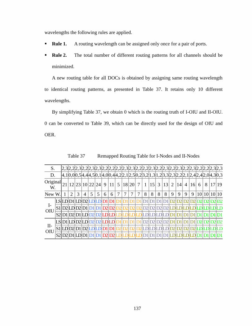
137
wavelengths the following rules are applied.
Rule 1. A routing wavelength can be assigned only once for a pair of ports.
Rule 2. The total number of different routing patterns for all channels should be
minimized.
A new routing table for all DOCs is obtained by assigning same routing wavelength
to identical routing patterns, as presented in Table 37. It retains only 10 different
wavelengths.
By simplifying Table 37, we obtain 0 which is the routing truth of I-OIU and II-OIU.
0 can be converted to Table 39, which can be directly used for the design of OIU and
OER.
Table 37 Remapped Routing Table for I-Nodes and II-Nodes
S. 2,3 2,2 2,3 2,2 2,3 2,3 2,2 2,2 2,2 2,3 2,3 2,2 2,2 2,3 2,2 2,3 2,2 2,3 2,2 2,3 2,2 2,2 2,3 2,3
D. 4,1 0,0 0,5 4,4 4,5 0,1 4,0 0,4 4,2 2,1 2,5 0,2 3,2 1,3 1,2 3,3 2,3 2,2 2,1 2,4 2,4 2,0 4,3 0,3
Original
W. 21 12 23 10 22 24 9 11 5 18 20 7 1 15 3 13 2 14 4 16 6 8 17 19
New W. 1 2 3 4 5 5 6 6 7 7 7 7 8 8 8 8 9 9 9 9 10 10 10 10
I-
OIU
LS LD D1 LD D2 LD LD D1 D1 D1 D1 D1 D1 D1 D1 D1 D1 D2 D2 D2 D2 D2 D2 D2 D2
S1 D2 LD D2 D1 D1 D1 D2 D2 D2 D2 D2 D2 D2 D2 D2 D2 LD LD LD LD LD LD LD LD
S2 D1 D2 D1 LD D2 D2 LD LD LD LD LD LD LD LD LD LD D1 D1 D1 D1 D1 D1 D1 D1
II-
OIU
LS D1 LD D2 LD D2 D2 LD LD D1 D1 D1 D1 D2 D2 D2 D2 D1 D1 D1 D1 D2 D2 D2 D2
S1 LD D2 D1 D2 LD LD D1 D1 D2 D2 D2 D2 LD LD LD LD D2 D2 D2 D2 LD LD LD LD
S2 D2 D1 LD D1 D1 D1 D2 D2 LD LD LD LD D1 D1 D1 D1 LD LD LD LD D1 D1 D1 D1

138
Table 38 Routing Table for OIU in GTON-XII
Wavelength 1 2 3 4 5 6 7 8 9 10
I-OIU
LS LD D1 LD D2 LD D1 D1 D1 D2 D2
S1 D2 LD D2 D1 D1 D2 D2 D2 LD LD
S2 D1 D2 D1 LD D2 LD LD LD D1 D1
II-OIU
LS D1 LD D2 LD D2 LD D1 D2 D1 D2
S1 LD D2 D1 D2 LD D1 D2 LD D2 LD
S2 D2 D1 LD D1 D1 D2 LD D1 LD D1
Table 39 Routing Table for OIU in GTON-XII
1 LD D1 D2
I-OIU
LS 1 3 5 2 6 7 8 4 9 10
S1 2 9 10 4 5 1 3 6 7 8
S2 4 6 7 8 1 3 9 10 2 5
II-OIU
LS 2 4 6 1 7 9 3 5 8 10
S1 1 5 8 10 3 6 2 4 7 9
S2 3 7 9 2 4 5 8 10 1 6
8.3.5 OIU Design
OIU which implements routing is a MRR-based optical-switch matrix. Based on the
Table 39, both I-OIU and II-OIU can be built with a series of optical switches as shown
in Figure 12.(c). The OIU is designed as follows:
1. Given the routing wavelengths in Table 39, add one or two MRR optical switch(es)
per wavelength into the basic OIU structure. The basic OIU structure has the port
connections as LSLD, S1D1 and S2D2, shown in Figure 74(a).
2. Each optical switch is added into the structure along with a cross-bridge as shown in
Figure 75to make the optical switch transparent to other wavelengths.
3. We define the following port pairs as the original routing pattern: LSLD, S1D1
and S2D2. Given the routing pattern of a wavelength, if it is same to the original

139
pattern (for example, w5 to I-OIU in Table 39), it can be disregarded. If its routing
pattern contains only one of the three pairs (for example, w1 to I-OIU in Table 39),
one MRR switch is to be added into the structure. If its routing pattern contains no
ports pair of the original pattern (for example, w6 and w7 to I-OIU in Table 39), two
MRR switches are to be added.
As an example, for wavelengths w1 and w2 in I-OIU, their routing patterns are given
in Table 40 and Table 41.
Table 40 Routing Table of Wavelength w1 in I-OIU
Wavelength LD D1 D2
I-OIU
LS 1
S1 1
S2 1
Table 41 Routing Table of Wavelength w2 in I-OIU
Wavelength LD D1 D2
I-OIU
LS 2
S1 2
S2 2
MRR switches associated with wavelength w1 and w2 can be integrated into I-OIU as
shown in Figure 74

140
Local
S end
S1
S2
Local
D end
D1
D2
(a) Direct source-destination ports connections in I-OIU.
Local
S end
S1
S2
Local
D end
D1
D2
w1
Block of
wavelength w1
(b) Integrating routing wavelength w1 into the I-OIU
Local
S end
S1
S2
Local
D end
D1
D2
Block of
wavelength w1
w1
w2
Block of
wavelength w2
(c) Integrating routing wavelength w2 into the I-OIU
Figure 74 Integrating single wavelength switches into OIU

141
wiOptical
Switch
Cross
Bridge
Figure 75 Optical switch and cross-bridge.
Based on the routing in Table 39, I-OIU and II-OIU are designed as shown in Figure
76.
(a). I-OIU
(b). II-OIU
Figure 76 I-OIU and II-OIU in GTON-XII
8.3.6 OER Design
The function of OER is to receive input optical signal and to convert it to electrical
data, then read and analyze the data header to make routing decision. If relay is necessary,
electrical to optical re-conversion is performed with a proper wavelength to transmit to

142
the next node. The OER in GTON-XII has 12 input and 12 output ports plus one input
port and one output port to the local core. Demultiplexers on both ends of the OER
separate multiple input optical signals and propagate each of them to the corresponding
input port. A photodetector in each channel receives input optical signal and converts it to
electrical data to the input buffer. The controller of the OER reads the header of a data
packet and determines the output channel the packet should go through. Packets
generated by a local core are stored in the input queue too.
In every OER, in each clock cycle, if an output channel is available, a packet will be
switched to the output channel through the crossbar, and then it is converted to the optical
signal and transmitted to next node. Packets destined to the local core will also be
switched similarly yet no EO conversion is required.
According to Table 39, the routing wavelengths assignment for all channels of I-Node
and II-Node is derived and shown in Figure 77.
(a) Wavelength assignment for I-Nodes
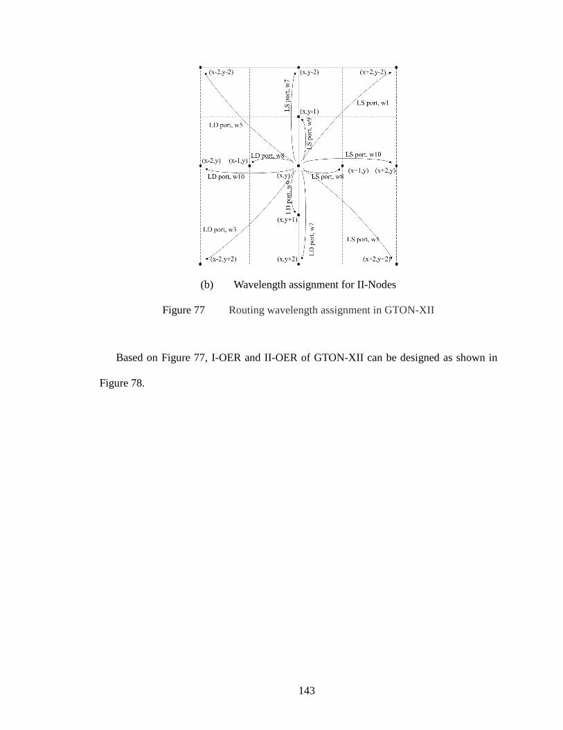
143
(b) Wavelength assignment for II-Nodes
Figure 77 Routing wavelength assignment in GTON-XII
Based on Figure 77, I-OER and II-OER of GTON-XII can be designed as shown in
Figure 78.

144
Crossbar
Switch
From Core
To Core
Local
S end
Local
D end
w9
w7
w10
w6
w9
w7
Mu
ltip
lex
er
driver
cou
ple
r
driverw10
w6
driver
driver
w8
w4
driver
receiverw8
Dem
ult
iple
xer
w9
w7
w10
w2
w6
w8
Dem
ult
iple
xer
w4
driver
w9
w7
Mu
ltip
lex
er
driver
driverw10
w2
driver
driver
w8
driver
w6
driver
receiver
receiver
receiver
receiver
receiver
receiver
receiver
receiver
receiver
receiver
receiver
cou
ple
r
S2 Channel Input Buffer
Local Input Buffer
Local Output Port
S1 Channel Input Buffer
E2 Channel Input Buffer
SE Channel Input Buffer
NE Channel Input Buffer
E1 Channel Input Buffer
N2 Channel Input Buffer
N1 Channel Input Buffer
W2 Channel Input Buffer
SW Channel Input Buffer
NW Channel Input Buffer
W1 Channel Input Buffer
S2 Channel Output Port
E2 Channel Output Port
SE Channel Output Port
NE Channel Output Port
E1 Channel Output Port
N2 Channel Output Port
N1 Channel Output Port
W2 Channel Output Port
SW Channel Output Port
NW Channel Output Port
W1 Channel Output Port
S1 Channel Output Port
(a) I-OER in GTON-XII

145
Crossbar
Switch
From Core
To Core
Local
S end
Local
D end
w9
w10
w7
w1
w9
w10
Mult
iple
xer
driver
couple
r
driverw7
w1
driver
driver
w8
w5
driver
receiverw8
Dem
ult
iple
xer
w9
w10
w7
w5
w3
w8
Dem
ult
iple
xer
w5
driver
w9
w10
Mult
iple
xer
driver
driverw7
w5
driver
driver
w8
driver
w3
driver
receiver
receiver
receiver
receiver
receiver
receiver
receiver
receiver
receiver
receiver
receiver
couple
r
N2 Channel Input Buffer
Local Input Buffer
Local Output Port
N1 Channel Input Buffer
E2 Channel Input Buffer
SE Channel Input Buffer
NE Channel Input Buffer
E1 Channel Input Buffer
S2 Channel Input Buffer
S1 Channel Input Buffer
W2 Channel Input Buffer
SW Channel Input Buffer
NW Channel Input Buffer
W1 Channel Input Buffer
N2 Channel Output Port
E2 Channel Output Port
SE Channel Output Port
NE Channel Output Port
E1 Channel Output Port
S2 Channel Output Port
S1 Channel Output Port
W2 Channel Output Port
SW Channel Output Port
NW Channel Output Port
W1 Channel Output Port
N1 Channel Output Port
(b) II-OER in GTON-XII
Figure 78 I-OER and II-OER structures in GTON-XII
8.3.7 Architecture Properties of GTON-XII
Table 42 summarizes the architectural properties of the GTON-XII.

146
Table 42 Architecture Properties of GTON-XII
Architecture Properties Value
Channels of each node 12
Lasers in each node 12
Photodetectors in each node 12
Routing wavelengths in each node 7
Total routing wavelengths in the network 10
MRRs in each node 28
MRR optical switches in each node 14
Electrical input queues in each node 12
Electrical output queues in each node 0
Optical buffers in each node 0
Optical couplers in each node 2
Electrical crossbar switches in each node 1
Optical wavelength multiplexers in each node 2
Optical wavelength demultiplexers in each node 2
TO/EO tuning devices in the network 0
8.4 Routing Algorithm of GTON-XII
The Johnson code is used in GTON-XII for node addressing and data routing.
8.4.1 Johnson Code Addressing for GTON-XII
To implement the data routing in the network the Johnson Code explained in Section
6.3 is applied for node addresses in GTON-XII.
8.4.1.1 Addressing Nodes in GTON-XII
The address of a node (Ah, Av) in the NN GTON-XII can be defined by means of two
n-bit Johnson Codes (Ch, Cv) where N=2n. For example, (3, 2) in a 66 GTON is
addressed as 011001. It is same as presented in Section 7.7.1.1.
8.4.1.2 Nodes Coordinates and Address Association
For a node address C = Ch|Cv, C is of N bits and N = 4n, Ch and Cv are both 2n bits. It

147
is same as presented in section 7.7.1.2.
8.4.2 Routing functions for GTON-XII
8.4.2.1 Routing Direction Function fr
In the routing algorithm, fr can be used to determine the routing direction, that is to
choose the next routing channel. It is same as the function fr presented in Section 7.7.2.1.
8.4.2.2 Routing Address Function fd
The Routing Address Function fd is to calculate the node address from the current
node address with an offset value. It is same as the function fd presented in Section
7.7.2.2.
8.4.2.3 Routing channel vector V
The routing channel vector V is used in routing a data packet from a source node to its
destinations. The format of vector V is as:
yx cccncnV ,,,,, 2233 (65)
where n3 is the number of Level3 channel c3, n2 is the number of Level3 channel c2, and
cx, cy are Level1 channels.
SWSENWNEc
NSWEc
NSc
WEc
y
x
,,,
2,2,2,2
1,1
1,1
3
2
(66)
Assume the source node address is (sh, sv) and the destination address is (dh, dv), fc
allows to derive the routing channel vector vvhhr dsdsfV ,,, based on the followings:
vvrvv
hhrhh
dsfcp
dsfcp
,,
,,
(67)

148
32
3
2,
2max
2,
2min
1&1
1&1
00
1&1
1&1
00
2mod
2mod
npp
n
ppn
hcifN
hcifS
hif
c
hcifW
hcifE
hif
c
ph
ph
vh
vh
yv
yv
y
y
xh
xh
x
x
vy
hx
(68)
0&1&1
0&1&1
0&1&1
0&1&1
00
3
3
3
3
3
3
nccifNW
nccifNE
nccifSW
nccifSE
nif
c
vh
vh
vh
vh
(69)
0&1&2
0&1&2
0&1&2
0&1&2
00
2
2
2
2
2
2
ncppifW
ncppifS
ncppifW
ncppifE
nif
c
hvh
hvh
vvh
vvh
(70)
8.4.2.4 Channel combination transforms in GTON-XII
From the topology view can be seen there are equal channel combination transforms
in GTON-XII as the following:

149
112
112
112
112
112
112
112
112
ESWWS
WSEES
ENWWN
WNEEN
NSWSW
SNWNW
NSESE
SNENE
(71)
and
22
22
22
22
NNNENW
WWNWSW
SSSWSE
EESENE
(72)
In general, given a routing vector, many isomeric routing vectors can be generated by
applying the equal channel combination transforms. The routing distances by these
routing vectors are same. This property will be used further in the adaptive routing
algorithm.
In addition, there are also numerous unequal channel combination transforms. It can
be seen that 12 channels in GTON-XII: i.e. 6 pairs, for example, channel E and W. By
adding any coupled two channels into any position of a given routing vector, its
destination will not change, though the routing distance increases. This property will also
be utilized in a later part of the paper.
8.4.3 Deterministic Routing Algorithm for GTON-XII
In deterministic routing, all transmissions should follow the sequence of Level3
channels first, Level2 channels second and Level1 channels last.
Also, before a data packet is sent from its source node, a routing path is determined
and stored as a routing channel vector V in the packet header. The routing vector is

150
composed of a sequence of channels. In each intermediary node, the router will read the
header, assign the output channel according to the routing vector V, and then update V to
remove the used channel and substitute the new V in the header.
The deterministic routing algorithm for GTON-XII can be formulated as shown in
Figure 79.
Figure 79 Deterministic routing algorithm for GTON-XII.
8.4.4 Adaptive Routing Algorithm for GTON-XII
In the adaptive routing, the routing path between a source and a destination is chosen
dynamically based on the buffer condition on each intermediary node. But the lengths of
Algorithm Routing (S→D):
Generate the routing vector V:
Routing:
if V=0
channel = internal
else
if c3 0
channel = c3, n3= n3-1
else
if c2 0
channel = c2, n2= n2-1
else
if cx 0
channel = cx, cx = 0
else
if cy 0
channel = cy, cy = 0
end
end
end
end
end
End

151
all different paths are maintained equal to the minimum distance between two nodes.
Here a new parameter Tc is introduced to describe the traffic condition in a node
which will be used for making a decision in the output channel.
Assume the number of data packets in the output buffer of channel x is nx, then
tx = B - nx (73)
where B is the maximum capacity of the buffer.
nwneswsennsswweec ttttttttttttT ,,,,,,,,,,, 21212121 (74)
In the basic adaptive dynamic routing, before the data packet arrives to its destination,
in each intermediary node the router reads the latest routing channel vector V, compares
the buffer conditions of channels in V to choose a best one, and updates the routing vector
V, as shown in Figure 80.
Figure 80 Adaptive routing algorithm for GTON-XII.
8.4.5 Fault Tolerant Routing Algorithm for GTON-XII
GTON-XII is featured by the fault tolerant ability because there are many alternative
routing paths between most of node pairs. This is due to 12 different channels and much
Algorithm Routing (S→D):
Generate the routing vector V:
Routing:
While V ≠ 0
In each intermediary node, check the traffic
condition of all available channels in the
routing vector V, then choose the best channel
for data routing.
Update V by removing the channel used from
the routing vector V.
End

152
equal channel combination transforms. For example, between (x, y) and (x+3, y+1) there
are 12 different routing paths, i.e.:
121
211
112
112
211
121
EES
EES
ESE
SEE
ESE
SEE
(75)
and
11
11
11
11
11
11
ESEN
SEEN
ENSE
NESE
NSEE
SENE
(76)
In this basic fault tolerant routing we have all routing distances equal to a shortest
distance between source and destination node. When a shortest path(s) between source
and destination nodes is blocked because of node/link failure, there are still many choices
for a path avoiding the failed spot. In the GTON-XII, only if all 12 neighbors of the
source or the destination are failed, the transmission fails.
The direct fault tolerant routing algorithm can be formulated as shown in Figure 81.

153
Figure 81 Direct fault tolerant routing algorithm for GTON-XII.
8.5 Simulation and Analysis
8.5.1 Simulation Setup
We test the maximum traffic load the network can handle without blocking. The
network is set to be homogeneous; and all nodes have the same packet generating rate.
The parameter setting of the simulation is shown in the Table 43.
Algorithm Routing (S→D):
Generate the routing vector V:
Routing:
While V ≠ 0
1. In each intermediary node, check the
buffer condition and availability of all
channels in the routing vector V, then route
through a channel with a lowest traffic.
2. If there is no available channel for
routing, do the equal channel combination
transform and repeat step 1 again.
3. If there are still no available channels for
routing, do the unequal channel transform
and then repeat step 1 again.
4. Update V by removing the used channel in
the routing vector V.
End
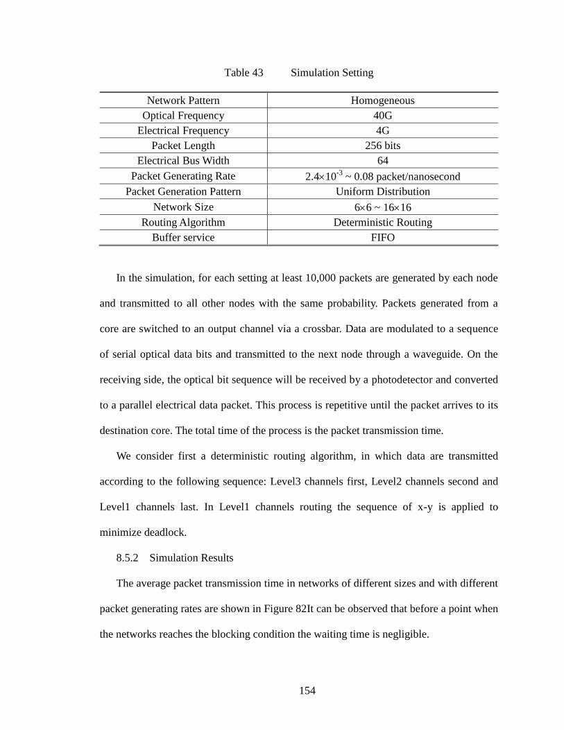
154
Table 43 Simulation Setting
Network Pattern Homogeneous
Optical Frequency 40G
Electrical Frequency 4G
Packet Length 256 bits
Electrical Bus Width 64
Packet Generating Rate 2.410-3
~ 0.08 packet/nanosecond
Packet Generation Pattern Uniform Distribution
Network Size 66 ~ 1616
Routing Algorithm Deterministic Routing
Buffer service FIFO
In the simulation, for each setting at least 10,000 packets are generated by each node
and transmitted to all other nodes with the same probability. Packets generated from a
core are switched to an output channel via a crossbar. Data are modulated to a sequence
of serial optical data bits and transmitted to the next node through a waveguide. On the
receiving side, the optical bit sequence will be received by a photodetector and converted
to a parallel electrical data packet. This process is repetitive until the packet arrives to its
destination core. The total time of the process is the packet transmission time.
We consider first a deterministic routing algorithm, in which data are transmitted
according to the following sequence: Level3 channels first, Level2 channels second and
Level1 channels last. In Level1 channels routing the sequence of x-y is applied to
minimize deadlock.
8.5.2 Simulation Results
The average packet transmission time in networks of different sizes and with different
packet generating rates are shown in Figure 82It can be observed that before a point when
the networks reaches the blocking condition the waiting time is negligible.

155
Figure 82 Average packet transmission time in GTON-XII
As it was mentioned before, each channel is equipped with an input buffer. The
average and maximum utilization of these buffers are shown in Figure 83and Figure 84
Figure 83 Average input buffer utilization in GTON-XII

156
Figure 84 Maximum input buffer utilization in GTON-XII
8.6 Network Properties of GTON Architectures
8.6.1 Buffer Analysis
The buffer usage is related to the channel usage. Level3 DOCs are used much more
frequently in a 12×12 GTON-XII than in a 6×6 GTON-XII when deterministic routing is
applied. In the 6×6 GTON-XII most of the traffic can be handled with Level1 & 2 DOCs.
Based on deterministic routing we have obtained the channel utilization in GTON-XII
of different sizes shown in Figure 85. It can be seen, when the network is smaller than
40×40, channel utilization percentiles are quite different. For high packet arrival rate
larger input buffer needed. On the other hand, routing algorithm can also affect the buffer
utilization.

157
Figure 85 Channel utilization in GTON-XII
8.6.2 Analysis of Channel Availability
Although the GTON supports wavelength multiplexing the optical interference occurs
if two signals of the same wavelength are transmitted from opposite ends of the DOC.
That can be avoided by first checking the waveguide serving condition before
transmission. When a channel is receiving it cannot be used to transmit simultaneously.
Hence the OER controller should monitor each channel and start transmission with an
idle channel only. A proper design in the MAC protocol would take care about issues
such as transmission at an even clock cycle from one side of a channel leaving the other
side an odd clock cycle. Here is a reasonable premise required that the network is
globally-synchronized.

158
8.6.3 Maximum DOC Length
As shown in Section 8.4, every DOC in GTON is built with a specific routing
wavelength and corresponding OIU and OER structures. In any DOC the internal routing
path of each OIU is different; otherwise a dead loop will occur. Consequently, the
maximum number of hops of a DOC is limited. For example, the OIU in GTON-XII has
6 ports, in which the 2 ports LS and LD are connected to OER. Other 4 ports have 2
combinations, i.e., (S1D1, S2D2) and (S1D2, S2D1) for both I-OIU and II-OIU.
Then totally four port combinations available for DOC routing, that indicates the
maximum length of a DOC is five hops. If OIU has 8 ports, the maximum distance is
seven hops. A DOC can be designed to connect any pair of nodes within this maximum
distance.
The performance of a GTON network is related to properties of the network topology,
such as diameter and average distance (number of hops, or number of O/E & E/O
conversions). And the GTON network topology is determined by how DOCs are
designed for each node in the network. Adding DOCs would lessen the transmission
delay, the energy consumption and improve fault tolerance; however would increase the
architecture/control complexity and the fabrication cost.
8.6.4 Topological Diversity of GTON
As explained in Sect.4, because DOC can be added between any two nodes, GTONs
can realize any topology. Although the proposed GTON architectures are 2D-Torus based,
the concept of DOC and OIU is not limited and can be extended to high-dimensional
topologies such as 3D-torus. Thus, GTON can be made high-dimensional and
consequently higher dimension topologies can be realized.

159
8.6.5 Transmission Power Loss
The optical power loss of the MRR switch matrix mainly is due to off-state, on-state
losses, waveguide crossing loss and waveguide propagation loss [23].
In our analysis, the waveguide propagation loss is neglected. Other loss values are
adopted according to [60], as shown in the Table 44. Transmission power losses in each
channel are listed in Table 45.
Table 44 Optical Power Budget
Component Loss(dB)
MRR off-state 0.06
MRR on-state 1.5
Waveguide Crossing 0.05
Photodetector 0.1
Table 45 Transmission Power Loss in DOCs
DOC I-Node II-Node
W. Power Loss (dB) W. Power Loss (dB)
E1 8 5.72 8 4.03
S1 9 7.15 9 7.15
W1 8 5.93 8 4.15
N1 9 4.63 9 3.91
E2 7 7.72 10 7.84
S2 10 7.84 7 7.72
W2 7 7.72 10 7.84
N2 10 5.06 7 7.72
NE 6 9.35 1 9.34
SE 4 7.81 5 7.79
SW 6 9.35 3 7.86
NW 2 7.81 5 7.79
Ave. 7.17 8.2
It can be seen from Table 45, transmission losses of Level1, 2 & 3 channels are

160
around 5.33dB, 7.43dB and 8.39dB, with maximum 9.35 dB and minimum 3.91 dB.
The channel transmission loss is linear to the distance of the channel, or OIUs in it.
The loss in each OIU relates to the number of MRR switches in it, which is linear to the
number of DOCs in each node. For example, in the GTON-XII each node has 12 DOCs,
consequently each OIU has 14 MRR switches. If the DOC number reduces to 8 by
removing all Level3 DOCs, there are only 8 MRR switches required in each OIU. Then
the power loss in each OIU is around 2.5 dB, and average power loss of all channels is
around 7.5dB. This will be a more applicable architecture with better cost/performance
tradeoff.
It can be seen from Figure 76 that many MRR switches in OIU are connected in
parallel. It is very suitable for applying the comb switch [85, 86], which will substantially
reduce the number of MRRs and consequently lesser the transmission loss.
In most of ONoC architectures which use MRR tuning, optical receivers have to deal
with a wide power range because the transmission power loss depends on the specific
path. Wide power range receivers are hard for practical implementation. In the GTON, on
contrast, the transmission power loss per DOC is constant, and thus the receiver is less
complex.
8.7 Conclusion
In this chapter a generalized 2D-torus based packet switching optical NoC
architecture called GTON is proposed with the use of micro-ring resonator (MRR) optical
switches. The complete schema to design a target network topology based on the GTON
is presented. The GTON is highly scalable because of packet switching. The use of
passive MRR switching, WDM and Direct Optical Channels offers an extremely high

161
bandwidth, low latency/ cost/power consumption, and makes the GTON fault tolerant
architecture. The performance of the network is evaluated by simulation. Related issues
such as analyses of channel utilization, transmission power loss and the buffer size are
also addressed. The GTON has shown many outstanding features which make it a
compelling solution for future optical NoCs.

162
CHAPTER 9
CONCLUSION
In this dissertation study, a set of different ONoC architecture are proposed for
different purposes with the adoption of wavelength division multiplexing and MRR
passive-switching routing. The first a group is with WRON, RDWRON and RCWRON
which are all fully connected network architectures.
To explore the topology advantage of different NoC architectures, an improved
version of RDT architecture, named QRDT is proposed for NoC applications. Compare
with traditional NoC topologies such as mesh, torus or hypercube, QRDT has better
flexibility, higher scalability and shorter network diameter and average distance, which is
suitable for ONoC applications.
By combining concepts from QRDT topology and WRON structure, a new ONoC
architecture family, 2D-torus based packet switching optical NoC architecture, or TON is
proposed. Three typical cases, TON-I, II, and III are presented and explained in detail.
And diverse routing algorithms are provided for each of them. Network performance of
each of them is presented with simulation results.
Based on the architecture family TON, a new generalized ONoC architecture,
generalized 2D-torus based packet switching optical NoC architecture, or GTON is
developed. Different to all existed architectures ever proposed, GTON is with high
scalability and infinite topology flexibility. Since GTON is of packet-switching, given a
limited number of different routing wavelengths, GTON can extend to any networks size
with the compensation of transmission latency. Followed with the design scheme
provided in 0, with the designated set up of proper DOCs and related OIUs, one or more

163
direct light path can be created between any two nodes in the network, hence GTON
architecture can be built into any given network topology.
In conclusion, with the use of passive switching MRR routing, WDM and Direct
Optical Channels, GTON architectures offered an extremely high bandwidth, low
latency/ cost/power consumption and robust fault tolerance. The performance of the
network is evaluated by simulation. Additional issues such as analyses of channel
utilization, transmission power loss and the buffer size are addressed as well. The GTON
has shown many outstanding features which make it a compelling solution for future
optical NoCs.
This study on ONoC architecture is still on-going. Now the study is concentrating
majorly on three topics. The first is the development of non-blocking WRON structure
based optical on-chip passive router. And some results are already submitted/accepted to
publish [87, 88]. The second is to apply the new MRR optical router to GTON
architecture to achieve a performance leap. Then the third is to further improve the
GTON performance by applying advanced routing algorithms and exploring more
network topologies. Shortly, working on such an exciting and promising field, more
complete works are expected to publish from time to time.

164
APPENDIX A
Proof of Propositions 1-3
For the convenience of proof, we represent the WRON using a diagonal grid structure,
and expand it to a Tri-network structure by adding two virtual WRONs at both sides of
the original WRON. We denote the original WRON as the Real WRON, the virtual
network close to the first (last) source node of the Real WRON as the Negative WRON
(Positive WRON). The Tri-network structure of N=4 is shown in Figure 86.
Each optical switch in the Tri-network is indicated by the coordinate (C,R) according
to Rule 1.
Rule 1. In the Real WRON, when j is odd, the coordinate of the ith
switch in the jth
stage is (j,2*i-1); when j is even, the coordinate of the ith
switch in the jth
stage is
(j,2*i).
In the Negative WRON, when j is odd, the coordinate of the ith
switch in the jth
stage is
(j,2*i-1-N); when j is even, the coordinate of the ith
switch in the jth
stage is (j,2*i-N).
In the Positive WRON, when j is odd, the coordinate of the ith
switch in the jth
stage is
(j,2*i-1+N); when j is even, the coordinate of the ith
switch in the jth
stage is (j,2*i+N).
Rule 2. At the up and bottom boundaries of the Real WRON, there are many Peak
Nodes as marked in Figure 87.
In the Real WRON, the coordinates of the Peak Node is indicated as (C, R), where C
is the stage number of the Peak Node and R equals to 0 (N) when the Peak Node is
connected to the first (last) switch in the stage.
Rule 3. When the routing path reaches the Peak Nodes in the network, if the
horizontal coordinate C of the Peak Nodes is same as the wavelength assigned to the

165
path, the path will change its routing direction and return to the Real WRON.
Otherwise, the routing path will keep its direction and move forward into one of the
virtual WRONs.
According to Rule 3, in solving the routing scheme, we shall try to avoid the trouble
arose by the veer of the routing path at some of the Peak Nodes.

166
Figure 86 Structure of the Tri-network for a 4×4 WRON.
All source and destination node addresses in the Tri-network are numbered following
Rule 4.
Rule 4. Every destination node address indicated in the Tri-network is the virtual

167
destination address D*. When the routing follows Rule 1, a routing path will reach the
virtual destination node D*. The relationship between the virtual addresses D* and its
corresponding real address D is shown below.
NDwhenDN
NDwhenD
DwhenD
D
**12
*0*
0**1
(77)
Similar to the source node, the relationship between the virtual addresses of source
node S* in the Tri-network and its corresponding real source address S is shown below.
NSwhenSN
NSwhenS
SwhenS
S
**12
*0*
0**1
(78)
For the ease of understanding, we have the following definitions.
Definition 1 (Start Node): The start node is the first node on the routing path
following the source node. It can be a switch node or a peak node.
Assume the source address for a routing path is S, then:
The coordinate of the start node is (1, S-1) if S is even, or (1, S) if S is odd.
Definition 2 (Reflection Node): The reflection node is the specified node in a routing
path whose horizontal coordinate is same as the wavelength assigned to the path. The
routing path will change its direction in the reflection node. There are two kinds of
reflection nodes: reflection peak node and reflection switch node. In any routing path
there is one and only one reflection node.
Definition 3 (Inherent Slope): The inherent slope is the slope of the routing path
starting from the source node to the reflection node.
Assume the source address for a routing path is S, then:

168
The inherent slope is -1 if S is even, or 1if S is odd.
Definition 4 (Acquired Slope): The acquired slope is the slope of the routing path
from the reflection node to the destination node. Obviously it is the opposite value of
the inherent slope.
Assume the source address for a routing path is S, then:
The acquired slope is 1 if S is even, or -1if S is odd.
Definition 5 (End Node): The end node is the last node on the routing path before the
destination node. It can be a switch node or a peak node.
Given an end node with the coordinate of (N, R), if the acquired slope is 1, the
destination node address is R+1; if the acquired slope is -1, the destination node address
is R.
In the following proof, we denote the coordinate of a node as (c,r) where r denote the
vertical coordinate and c denote the horizontal coordinate.
A.1. Proof of Proposition 1
In an N-WRON, given the source node address S and the routing wavelength W, the
destination address D can be derived by the following procedure.
When N is Even
Case 1. When S is even
The coordinate of the start node is (1,S-1). The inherent slope is -1. The function of
the routing path before the reflection node is (r-(S-1))+(c-1)=0, i.e., r=S-c.
Given the routing wavelength W, let c=W, then r=c-W. Hence the coordinate of the
reflection node is (S-W,W).
Hence the function of the routing path after the reflection node is (r-(S-W))-(c-W)=0,

169
i.e., r=S+c-2×W
The vertical coordinate of the end node is N, hence the horizontal coordinate of the
end node is r=S+N-2×W.
Then the virtual address D* of the destination node is
D* = S + (N - 2W + 1).
Case 2. When S is odd
By the procedure similar to case 1, when S is odd, the virtual address of the
destination node can be derived as
D* = S - (N - 2W + 1).
In summary, D* = S + (N - 2W + 1)×(-1)S.
When N is Odd
By the same way as in Case 1, when N is odd, the virtual address D* of the
destination node can be derived as
D* = S + (N - 2W + 1)×(-1)S.
Hence Proposition 1 holds. ■
A.2. Proof of Proposition 2
When N is even:
Case 1. When D is even
Similar to the cases in Appendix I, the virtual address of the source node can be
derived as
S* = D + (N - 2W + 1).
Case 2. When D is odd
The virtual address of the source node can be derived as

170
S* = D - (N - 2W + 1).
In summary, S* = D - (N - 2W + 1)×(-1)N+D
.
When N is odd:
The virtual address of the destination node can be derived as
S* = D - (N - 2W + 1)×(-1)N+D
.
Hence Proposition 2 holds. ■
A.3. Proof of Proposition 3
For an N-WRON, given the source node address S and the destination node address D,
the routing wavelength W can be derived based on S as follows. The major problem in
deriving W is that sometimes we should not use the real address D but the virtual address
D* in computing the correct wavelength W.
When N is even
When S and D have different parities, the destination node of the routing path is in the
Real WRON, i.e., D*=D.
Case 1. When S is even
When D is odd, D*=D. The coordinate of the start node is (1, S-1), the inherent slope
is -1. The function of the path before the reflection node is r-S+c=0.
The coordinate of the end node is (N,D-1). The acquired slope is 1. The function of
the routing path after the reflection node is r-(D-1)=c-N, i.e., r-D-1+N+c=0.
Assume the reflection node is in (c0,r0), then
2
1
2
1
01
00
00
00 DSNW
DSNc
NDcr
Scr
When D is even, the destination node is in the Virtual WRON, i.e., D*≠D. There have
two possibilities: D*>N or D*≤0. Hence the routing wavelength W for the path from

171
source node S to destination node D should be:
2
*1 DSNW
,
where
0*1*
*12*
DwhenDD
NDwhenDND
Then we have
22
11
22
121
2
1
NDSDSNW
NDSDNSNW
The wavelength W should be greater than 0 and less than N, hence we have the
following expressions:
NDSNDSN
NW
NDSW
3
0
2
1
1
NDSNDSN
NW
NDSW
2
2
0
2
Then W=W1 when S+D>N and W=W2 when S+D≤N.
Case 2. When S is odd
It can be derived similarly to Case 1, when D is even
2
1 DSNW
When D is odd,

172
22
2
22
23
NDSwhenNDS
W
NDSwhenNDS
W
When N is Odd
When S and D have same parities, the destination node of the routing path is in the
Real WRON, i.e., D*=D.
Case 1. When S is even
Similar to the last case, when D is even,
2
1 DSNW
When D is odd,
NDSwhenNDS
W
NDSwhenNDS
W
2
2
Case 2. When S is odd
Similar to the case 1, when D is odd,
2
1 DSNW
.
When D is even,
22
2
22
23
NDSwhenNDS
W
NDSwhenNDS
W
Hence Proposition 3 holds. ■

173
APPENDIX B
Proof of Propositions 4-6
All rules and definitions used here are same as in Appendix 0
B.1. Step I
Consider the topology structure of the WRON as shown in Figure 87. Each switch is
indicated by its coordinate (c,r) uniquely in the. When the routing wavelength w assigned
to the routing path is different to all the wavelengths presnet in the WRON, we refer this
situation as the “The N-WRON is irrelative to the wavelength w”. When the N-WRON is
irrelative to the wavelength, the relationship between the address of the source node S
and the address of the destination node address D can be derived as D = N-S+1.

174
Figure 87 Structure of 8-WRON.
B.2. Step II
When an N-WRON is connected with an Inverse Connector (IC), there are two types
of connections between IC and N-WRON as shown in Figure 88.

175
(a)
(b)
Figure 88 Two type of connections between IC and WRON.
Given the size of IC N, the address of source node S, when the N-WRON is irrelative
to the wavelength, the destination node address is derived as: D=N+1–S.
The routing truth of the subnet shown in Figure 89 is given by:
sdmNd
sNm
1
1
Hence both sub-networks shown in Figure 89 can be substituted as the Straight
Connection (SC) block (Figure 90).

176
Figure 89 Straight connection block.
Note that the integration of any number of N-SCs is equal to one N-SC and the
integration of N-SC to other network (WRON) is equal to that network (WRON).
B.3. Step III
Given any N2-RDWRON and a wavelength w assigned to a special routing path, we
can easily transform the RDWRON to a WRON by the following way.
In the N2-RDWRON, there are N N-WRON and N-1 IC blocks. Assume that
N
wk
1
, 1,1mod0 Nww .
Then the wavelength w exists only in the (k+1)th
N-WRON, i.e., all other k-1 N-
WRONs are irrelative to the wavelength w.
For the ith
N-WRON, 0<i<k, in the N2-RDWRON, it can be integrated with the i
th IC
to an N-SC; for the jth
N-WRON, k<j≤N, in the N2-RDWRON, it can be integrated with
the (j-1)th
IC to an N-SC too. Then the N2-RDWRON is composed only of SCs and
WRONs which can be treated as WRON merely. This process is shown in Figure 90.
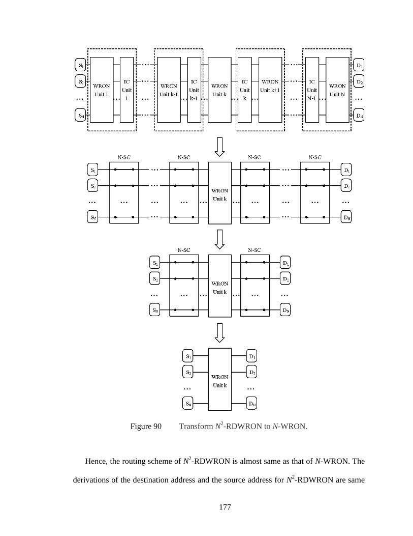
177
Figure 90 Transform N2-RDWRON to N-WRON.
Hence, the routing scheme of N2-RDWRON is almost same as that of N-WRON. The
derivations of the destination address and the source address for N2-RDWRON are same

178
as those for N-WRON. In deriving the routing wavelength, we can treat the N2-
RDWRON as N different N-WRON and calculate them separately.
We summarize the routing scheme of RDWRON as follows.
For an N2-RDWRON, given the source node address S and the routing wavelength w,
the destination node address D can be derived as follows.
D = fD (N, S, w0)
where w0 = mod (w-1, N) + 1, and fD is the function defined in Eqn. (3).
For an N2-RDWRON, given the destination node address D and the routing
wavelength w, the source node address S can be derived as following.
S = fS (N, D, w0)
where w0 = mod (w-1, N) + 1, and fD is the function defined in Eqn. (4).
In an N2-RDWRON, a set of different routing wavelengths can be used in routing
from one source node to one destination node. Denote the set of different wavelengths of
the N2-RDWRON as W, given the RDWRON size N, the source node address S and the
destination node address D, W can be derived as:
NkNkw
NNwNNwNwNwwW
,,2,11
1,2,,2,,
where w = fw (N, S, D), and fD is the function defined in Eqn. (5).
Hence, Proposition 4 to Proposition 6 hold. ■

179
APPENDIX C
Proof of Lemma 7 and Lemma 8
C.1. Proof of Lemma 7
To prove the lemma, we first introduce the Quad-Star Network (QSN). An N-QSN is
constructed based on a (2N+1)x(2N+1) mesh by removing all nodes with their minimum
distance (in number of hops) to the center node (indexed as (N, N)) greater than N and
their related links. Figure 91 shows the structure of a 3-QSN, with the center node (C)
and an edge node (E) marked. The minimum distance between C and E is 3 hops.
In an n-QSN, the total number of nodes in the network is given by
1221
2
14
11214
2
nnnn
nnnU
(79)
C E
Figure 91 Structure of 3-QSN.
And the sum of lengths (in number of hops) of all shortest paths between all nodes in

180
the network to C is
3
1212
6
1214
1214 2222
nnn
nnn
nnnD
(80)
Figure 92 shows that the 12-QRDT is partitioned into 8 QSNs in different sizes
(shown in different colored regions) based on their respective location to the original
node O (the node at the left-up corner). Some of the QSNs are overlapped. In general, for
an N-QRDT, it can be partitioned to one n-QSN (B in Figure 92), four n-QSN (F1, F2, F3,
and F4 in Figure 92) and three (n-1)-QSN (S1, S2, and S3 in Figure 92), where n=N/4.

181
S2
S3
S2
B
B
S3
S1
F3
F1 F2
F4
B
BO
X
P
Q
R T
Figure 92 Partition of QRDT to QSNs.
Consider the n-QSN region B in Figure 92. Then the rank-0 path between any node in
B and the original node O is less than or equal to n hops. According to the JCVR
algorithm, the routing path between any node in B and the original node O is less than n.
Then consider the n-QSN regions F1, F2, F3, and F4. The rank-0 path between any
node in these regions and their center node is less than or equal to n hops. According to
the JCVR algorithm, the routing path between any node in F1, F2, F3 and F4 to the
original node O is less than n+1.
S1, S2, and S3 are (n-1)-QSNs. All rank-0 paths between nodes in these regions to their
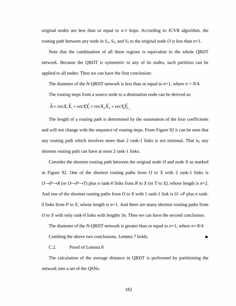
182
original nodes are less than or equal to n-1 hops. According to JCVR algorithm, the
routing path between any node in S1, S2, and S3 to the original node O is less than n+1.
Note that the combination of all these regions is equivalent to the whole QRDT
network. Because the QRDT is symmetric to any of its nodes, such partition can be
applied to all nodes. Then we can have the first conclusion:
The diameter of the N-QRDT network is less than or equal to n+1, where n = N/4.
The routing steps from a source node to a destination node can be derived as
00001111 YvecYXvecXYvecYXvecXA
.
The length of a routing path is determined by the summation of the four coefficients
and will not change with the sequence of routing steps. From Figure 92 it can be seen that
any routing path which involves more than 2 rank-1 links is not minimal. That is, any
shortest routing path can have at most 2 rank-1 links.
Consider the shortest routing path between the original node O and node X as marked
in Figure 92. One of the shortest routing paths from O to X with 2 rank-1 links is
O→P→R (or O→P→T) plus n rank-0 links from R to X (or T to X), whose length is n+2.
And one of the shortest routing paths from O to X with 1 rank-1 link is O→P plus n rank-
0 links from P to X, whose length is n+1. And there are many shortest routing paths from
O to X with only rank-0 links with lengths 3n. Then we can have the second conclusion:
The diameter of the N-QRDT network is greater than or equal to n+1, where n=N/4
Combing the above two conclusions, Lemma 7 holds. ■
C.2. Proof of Lemma 8
The calculation of the average distance in QRDT is performed by partitioning the
network into a set of the QSNs.

183
According to the proof of Lemma 1, by the JCVR algorithm, the total lengths of all
shortest paths between one selected node and all other nodes are
23
3220
3
32
1213
14144
23
nnn
nUnD
nnUnnnDnDSum
(81)
And the number of all such paths is N2 – 1 = 16n
2 - 1.
Then the average distance between one selected node and all other nodes is
116
23
3220
3
32
116
121314144
2
23
2
n
nnn
n
nUnDnnUnnnDnDd
(82)
As the N-QRDT is a symmetric network, the average distance of N-QRDT is also d.
Hence Lemma 8 holds. ■

184
REFERENCES
[1] (2010). International Technology Roadmap for Semiconductors.
[2] D. Yeh, et al., "Thousand-Core Chips," Design & Test of Computers, IEEE, vol.
25, pp. 272-278, 2008.
[3] A. Shacham, et al., "Photonic Networks-on-Chip for Future Generations of Chip
Multiprocessors," IEEE Transactions on Computers, vol. 57, pp. 1246-1260,
2008.
[4] H. Gu, et al., "A Low-power Low-cost Optical Router for Optical Networks-on-
Chip in Multiprocessor Systems-on-Chip," in IEEE Computer Society Annual
Symposium on VLSI, 2009. ISVLSI '09, 2009, pp. 19-24.
[5] N. Kirman, et al., "Leveraging Optical Technology in Future Bus-based Chip
Multiprocessors," in Microarchitecture, 2006. MICRO-39. 39th Annual
IEEE/ACM International Symposium on, 2006, pp. 492-503.
[6] G. I. Papadimitriou, et al., "Optical switching: switch fabrics, techniques, and
architectures," Lightwave Technology, Journal of, vol. 21, pp. 384-405, 2003.
[7] G. Chen, et al., "Electrical and optical on-chip interconnects in scaled
microprocessors," in Circuits and Systems, 2005. ISCAS 2005. IEEE International
Symposium, 2005, pp. 2514-2517.
[8] A. Shacham, et al., "Photonic NoC for DMA Communications in Chip
Multiprocessors," in High-Performance Interconnects, 2007. HOTI 2007. 15th
Annual IEEE Symposium, 2007, pp. 29-38.
[9] http://www.optics-news.com/.

185
[10] I. O‟Connor, "Unconventional interconnects: Optical solutions for system-level
interconnect," in Proceeding of International Workshop in System Level
Interconnect Prediction, 2004, pp. 79-88.
[11] B. E. Little, et al., "Wavelength switching and routing using absorption and
resonance," Photonics Technology Letters, IEEE, vol. 10, pp. 816-818, 1998.
[12] A. Sakai, et al., "Low loss ultra-small branches in a silicon photonic wire
waveguide," IEICE TRANSACTIONS on Electronics, vol. E85-C, pp. 1033-1038,
2002.
[13] N. G. Rouskas, Routing and wavelength assignment in optical WDM networks, 1st
ed.: John Wiley & Sons, 2001.
[14] N. Sherwood-Droz, et al., "Optical 4x4 hitless Silicon router for optical
Networks-on-Chip (NoC)," Optics Express, vol. 16, pp. 19395-19395, 2008.
[15] R. S. Patti, "Three-Dimensional Integrated Circuits and the Future of System-on-
Chip Designs," Proceedings of the IEEE, vol. 94, pp. 1214-1224, 2006.
[16] V. F. Pavlidis and E. G. Friedman, "Interconnect-Based Design Methodologies
for Three-Dimensional Integrated Circuits," Proceedings of the IEEE, vol. 97, pp.
123-140, 2009.
[17] http://www.ibm.com/.
[18] R. Ramaswami, et al., "Optical Networks: A Practical Perspective," 3rd
ed:
Morgan Kaufmann Pub, 2009.
[19] T. Mudge, "Power: a first-class architectural design constraint," Computer, vol.
34, pp. 52-58, 2001.

186
[20] A. Shacham, et al., "On the Design of a Photonic Network-on-Chip," in First
International Symposium on Networks-on-Chip, 2007. NOCS 2007, 2007, pp. 53-
64.
[21] S. Xiao, et al., "Multiple-channel silicon micro-resonator based filters for WDM
applications," Optics Express, vol. 15, pp. 9386-9386, 2007.
[22] http://www.intel.com/.
[23] A. W. Poon, et al., "Cascaded Microresonator-Based Matrix Switch for Silicon
On-Chip Optical Interconnection," Proceedings of the IEEE, vol. 97, pp. 1216-
1238, 2009.
[24] A. Liu, "Announcing the world's first 40G silicon laser modulator," presented at
the http://blogs.intel.com/research/, 2007.
[25] M. Lipson, "Compact Electro-Optic Modulators on a Silicon Chip," IEEE Journal
of Selected Topics in Quantum Electronics, vol. 12, pp. 1520-1526, 2006.
[26] J. K. Poon, et al., "Transmission and group delay of microring coupled-resonator
optical waveguides," Optics Letters, vol. 31, pp. 456-458, 2006.
[27] J. Liu, et al., "Ge-on-Si laser operating at room temperature," Optics Letters, vol.
35, pp. 679-681, 2010.
[28] S. Assefa, et al., "CMOS-integrated high-speed MSM germanium waveguide
photodetector," Optics Express, vol. 18, pp. 4986-4999, 2010.
[29] S. Assefa, et al., "Reinventing germanium avalanche photodetector for
nanophotonic on-chip optical interconnects," Nature, vol. 464, pp. 80-84, 2010.
[30] H. Rong, et al., "A continuous-wave Raman silicon laser," Nature, vol. 433, pp.
725-728, 2005.

187
[31] H. Rong, et al., "An all-silicon Raman laser," Nature, vol. 433, pp. 292-294,
2005.
[32] H. Rong, et al., "Low-threshold continuous-wave Raman silicon laser," Nature
Photonics, vol. 1, pp. 232-237, 2007.
[33] Y. Onishi, et al., "Long-Wavelength GaInNAs Vertical-Cavity Surface-Emitting
Laser With Buried Tunnel Junction," IEEE Journal of Selected Topics in
Quantum Electronics, vol. 15, pp. 838-843, 2009.
[34] K. Iga, "Surface-emitting laser-its birth and generation of new optoelectronics
field," IEEE Journal of Selected Topics in Quantum Electronics, vol. 6, pp. 1201-
1215, 2000.
[35] C. J. Chang-Hasnain, et al., "Multiple wavelength tunable surface-emitting laser
arrays," IEEE Journal of Quantum Electronics, vol. 27, pp. 1368-1376, 1991.
[36] http://www.wsi.tum.de/.
[37] B. R. Koch, et al., "A 40 GHz Mode Locked Silicon Evanescent Laser," presented
at the 4th IEEE International Conference on Group IV Photonics, 2007, 2007.
[38] B. R. Koch, et al., "Mode-locked silicon evanescent lasers," Optics Express, vol.
15, pp. 11225-11233, 2007.
[39] G. V. Treyz, et al., "Silicon Mach–Zehnder waveguide interferometers based on
the plasma dispersion effect," Applied Physics Letters, vol. 59, pp. 771-773, 1991.
[40] C. Z. Zhao, et al., "Silicon on insulator Mach-Zehnder waveguide interferometers
operating at 1.3 um," Applied Physics Letters, vol. 67, pp. 2448-2449, 1995.

188
[41] P. Dainesi, et al., "CMOS compatible fully integrated Mach-Zehnder
interferometer in SOI technology," Photonics Technology Letters, IEEE, vol. 12,
pp. 660-662, 2000.
[42] A. Liu, et al., "A high-speed silicon optical modulator based on a metal-oxide-
semiconductor capacitor," Nature, vol. 427, pp. 615-618, 2004.
[43] R. Soref and B. Bennett, "Electrooptical effects in silicon," IEEE Journal of
Quantum Electronics, vol. 23, pp. 123-129, 1987.
[44] A. Irace, et al., "All-silicon optoelectronic modulator with 1 GHz switching
capability," Electronics Letters, vol. 39, pp. 232-233, 2003.
[45] C. A. Barrios, et al., "Electrooptic modulation of silicon-on-insulator
submicrometer-size waveguide devices," Lightwave Technology, vol. 21, pp.
2332-2339, 2003.
[46] C. E. Png, et al., "Optical phase modulators for MHz and GHz modulation in
silicon-on-insulator (SOI)," Journal of lightwave technology, vol. 22, pp. 1573-
1582, 2004.
[47] B. R. Hemenway, et al., "All silicon integrated optical modulator for 1.3 um fiber-
optic interconnects," Applied Physics Letters, vol. 55, pp. 349-350, 1989.
[48] L. Gu, et al., "High-speed electro-optical silicon modulators based on photonic
crystal waveguides," presented at the Silicon Photonics II. Proceedings of the
SPIE, 2007.
[49] A. Liu, "Silicon Photonic Modulator Transmits Data at 30 Gb/s," presented at the
http://blogs.intel.com/research/, 2007.

189
[50] Q. Xu, et al., "Cascaded silicon micro-ring modulators for WDM optical
interconnection," Optics Express, vol. 4, pp. 9431-9435, 2006.
[51] B. Ciftcioglu, et al., "3-GHz Silicon Photodiodes Integrated in a 0.18um CMOS
Technology," Photonics Technology Letters, IEEE, vol. 20, pp. 2069-2071, 2008.
[52] S. Assefa, et al., "CMOS-Integrated 40GHz Germanium Waveguide
Photodetector for On-Chip Optical Interconnects," presented at the Optical Fiber
Communication Conference, OSA Technical Digest (CD) (Optical Society of
America), 2009.
[53] B. E. Little, et al., "Micro-ring resonator channel dropping filters," in Lasers and
Electro-Optics Society Annual Meeting, 1995. 8th Annual Meeting Conference
Proceedings, Volume 1., IEEE, 1995, pp. 233-234 vol.2.
[54] L. Zhang, et al., "Architectures and Routing Schemes for Optical Network-on-
Chips," Computers & Electrical Engineering, vol. 35, pp. 856-877, 2009.
[55] M. Briere, et al., "Design and behavioral modeling tools for optical network-on-
chip," in Design, Automation and Test in Europe Conference and Exhibition,
2004. Proceedings, 2004, pp. 738-739.
[56] B. E. Little, et al., "Microring resonator arrays for VLSI photonics," Photonics
Technology Letters, IEEE, vol. 12, pp. 323-325, 2000.
[57] J. Xue, et al., "An Intra-Chip Free-Space Optical Interconnect," in Proceeding of
37th
Annual International Symposium on Computer Architecture, 2010, pp. 94-
105.
[58] H. Wang, et al., "Nanooptical Optical Interconnection Network Architecture for
On-Chip and Off-Chip Communications," presented at the Optical Fiber

190
Communication Conference and Exposition and The National Fiber Optic
Engineers Conference, 2008.
[59] H. Gu, et al., "A Low-power Low-cost Optical Router for Optical Networks-on-
Chip in Multiprocessor Systems-on-Chip," in VLSI, 2009. ISVLSI '09. IEEE
Computer Society Annual Symposium, 2009, pp. 19-24.
[60] C. Batten, et al., "Building Manycore Processor-to-DRAM Networks with
Monolithic Silicon Photonics," in High Performance Interconnects, 2008. HOTI
'08. 16th IEEE Symposium on, 2008, pp. 21-30.
[61] J. M. Cianchetti, et al., "Phastlane: a rapid transit optical routing network,"
in ISCA '09, Proceedings of the 36th
annual international symposium on
Computer architecture, 2009, pp. 441-450.
[62] Y. Pan, et al., "Firefly: illuminating future network-on-chip with nanophotonics,"
in ISCA '09, Proceedings of the 36th
annual international symposium on
Computer architecture, 2009, pp. 429-440.
[63] A. Joshi, et al., "Silicon-photonic clos networks for global on-chip
communication," in Networks-on-Chip, 2009. NoCS 2009. 3rd ACM/IEEE
International Symposium on, 2009, pp. 124-133.
[64] D. Vantrease, et al., "Corona: System Implications of Emerging Nanophotonic
Technology," in Computer Architecture, 2008. ISCA '08. 35th International
Symposium on, 2008, pp. 153-164.
[65] M. Briere, et al., "System Level Assessment of an Optical NoC in an MPSoC
Platform," in Design, Automation & Test in Europe Conference & Exhibition,
2007. DATE '07, 2007, pp. 1-6.

191
[66] N. Kirman and J. F. Mart, "A power-efficient all-optical on-chip interconnect
using wavelength-based oblivious routing," ACM SIGARCH Computer
Architecture News - ASPLOS '10, vol. 38, pp. 15-28, 2010.
[67] H. Gu, et al., "A low-power fat tree-based optical Network-On-Chip for
multiprocessor system-on-chip," in Design, Automation & Test in Europe
Conference & Exhibition, 2009. DATE '09., 2009, pp. 3-8.
[68] A. Shacham and K. Bergman, "An Experimental Validation of a Wavelength-
Striped, Packet Switched, Optical Interconnection Network," Lightwave
Technology, vol. 27, pp. 841-850, 2009.
[69] F. Xia, et al., "Ultra-compact high order ring resonator filters using submicron
silicon photonic wires for on-chip optical interconnects," Optics Express, vol. 15,
pp. 11934-11941, 2007.
[70] G. Huaxi, et al., "A low-power fat tree-based optical Network-On-Chip for
multiprocessor system-on-chip," in Design, Automation & Test in Europe
Conference & Exhibition, 2009. DATE '09., 2009, pp. 3-8.
[71] B. E. Little, et al., "Ultra-compact Si-SiO2 microring resonator optical channel
dropping filters," Photonics Technology Letters, IEEE, vol. 10, pp. 549-551,
1998.
[72] B. R. Koch, et al., "A 40 GHz Mode Locked Silicon Evanescent Laser," in Group
IV Photonics, 2007 4th IEEE International Conference on, 2007, pp. 1-3.
[73] M. Haurylau, et al., "On-Chip Optical Interconnect Roadmap: Challenges and
Critical Directions," IEEE Journal of Selected Topics in Quantum Electronics,
vol. 12, pp. 1699-1705, 2006.

192
[74] N. Nelson, et al., "Alleviating Thermal Constraints while Maintaining
Performance Via Silicon-Based On-Chip Optical Interconnects," in Proceedings
of Workshop on Unique Chips and Systems, 2005, pp. 45-52.
[75] L. Benini and G. De Micheli, "Networks on chips: a new SoC paradigm,"
Computer, IEEE Journal, vol. 35, pp. 70-78, 2002.
[76] T. Bjerregaard and S. Mahadevan, "A survey of research and practices of
Network-on-chip," ACM Comput. Surv., vol. 38, p. 1, 2006.
[77] M. Millberg, et al., "The Nostrum backbone-a communication protocol stack for
Networks on Chip," in 17th International Conference on VLSI Design, 2004.
Proceedings, 2004, pp. 693-696.
[78] T. Marescaux, et al., "Interconnection Networks Enable Fine-Grain Dynamic
Multi-tasking on FPGAs," presented at the Proceedings of the Reconfigurable
Computing Is Going Mainstream, 12th International Conference on Field-
Programmable Logic and Applications, 2002.
[79] P. Guerrier and A. Greiner, "A generic architecture for on-chip packet-switched
interconnections," in Design, Automation and Test in Europe Conference and
Exhibition 2000. Proceedings, 2000, pp. 250-256.
[80] Y. Yu, et al., "A RDT-based interconnection network for scalable network-on-
chip designs," in Information Technology: Coding and Computing, 2005. ITCC
2005. International Conference, 2005, pp. 723-728.
[81] T. Dumitras, et al., "Towards on-chip fault-tolerant communication," in Design
Automation Conference, 2003. Proceedings of the ASP-DAC 2003. Asia and
South Pacific, 2003, pp. 225-232.

193
[82] L. Zhang, et al., "A 2D-Torus Based Packet Switching Optical Network-on-Chip
Architecture," presented at the accepted by the IEEE International Symposium on
Photonics and Optoelectronics (SOPO 2011), 2011.
[83] L. Zhang, et al., "Packet Switching Optical Network-on-Chip Architectures,"
submitted to Special Issue "Emerging Computing Architectures and Systems" of
the Journal “Computer and Electrical Engineering”, Mar. 2011.
[84] L. Zhang, et al., "A Generalized Packet Switching Optical Network-on-Chip
Architecture," submitted to Special Issue on On-Chip and Off-Chip Network
Architectures - ACM Transactions on Embedded Computing Systems, Feb. 2011.
[85] P. Dong, et al., "All-optical compact silicon comb switch," Optics Express, vol.
15, pp. 9600-9605, 2007.
[86] B. G. Lee, et al., "All-Optical Comb Switch for Multiwavelength Message
Routing in Silicon Photonic Networks," Photonics Technology Letters, IEEE, vol.
20, pp. 767-769, 2008.
[87] X. Tan, et al., "On a Scalable, Non-Blocking Optical Router for Photonic
Networks-on-Chip Designs," presented at the accepted by the IEEE International
Symposium on Photonics and Optoelectronics (SOPO 2011), 2011.
[88] X. Tan, et al., "A Generic Optical Router Design for Photonic Network-on-
Chips," submitted to IEEE/OSA Journal of Lightwave Technology, Mar. 2011.

194
VITA
Graduate College
University of Nevada, Las Vegas
Lei Zhang
Degrees:
Bachelor of Science, 1997
Yanshan University, China
Master of Science, 2004
Tianjin University, China
Special Honors and Awards:
UNLV, College Best Dissertation Award, 2nd
place, 2011
UNLV Summer Scholarship, 2010
UNLV President‟s Graduate Fellowship, 2008
UNLV Graduate Research and Training (GREAT) Assistantship, 2007
Outstanding Student of Tianjin University, China, 2003
Outstanding Quality Control Team Member, Ministry of Transportation, China, 2001
Outstanding Employee of Qinhuangdao Port Group, China, 1998 & 1999
Publications:
Journal Articles
[1] Xianfang Tan, Mei Yang, Lei Zhang, Yingtao Jiang, Jianyi Yang, "A Generic
Optical Router Design for Photonic Network-on-Chips," submitted to IEEE/OSA
Journal of Lightwave Technology on Mar.31, 2011.
[2] Lei Zhang, Emma E. Regentova and Xianfang Tan, “Packet Switching Optical
Network-on-Chip Architectures”, submitted to the Special Issue on Emerging
Computing Architectures and Systems of Journal Computers and Electrical
Engineering on Mar.10, 2011.
[3] Lei Zhang, Emma E. Regentova and Xianfang Tan, “A Generalized Optical
Network-on-Chip Architecture”, submitted to Special Issue on On-Chip and Off-
Chip Network Architectures of ACM Transactions on Embedded Computing
Systems on Feb.28, 2011
[4] Lei Zhang, Mei Yang, Yingtao Jiang and Emma E. Regentova, “Architectures
and Routing Schemes for Optical Network-on-Chips”, Computers & Electrical
Engineering, Vol. 35, Issue 6, Nov. 2009, pp. 856-877.
[5] Lei Zhang, Yingtao Jiang and Emma E. Regentova, “Fault Tolerance Routing for
Wavelength Routed Optical Networks in ONoC,” International Journal of
Computers and Applications, Vol. 30, Issue 1, March 2008. pp. 23-35.
[6] Emma E. Regentova, Lei Zhang, Vijay K. Mandava, Ajay K. Mandava, Gongyin
Chen and Zane Wilson, “Radioscopic Inspection of Nuclear Materials in Cargo

195
Containers with Dual-Megavoltage Energy Barriers”, accepted by Journal of
Nuclear Science and Engineering on Feb. 2010.
[7] Emma E. Regentova, Lei Zhang, Ajay K. Mandava, Gongyin Chen and Zane
Wilson, “Advantages and Challenges of Radioscopic Detection of Nuclear
Materials in Cargo Containers with Two Megavoltage Energy Barriers”, to be
appeared on the Journal of IEEE Transactions on Systems on July, 2011.
[8] Emma E. Regentova, Lei Zhang, Jun Zheng and Gopalkrishna Veni,
“Microcalcification Detection Based on Wavelet Domain Hidden Markov Tree
Model: Study for inclusion to computer aided diagnostic prompting system”,
Medical Physics, June 2007, Vol. 34, Issue 6, pp. 2206-2219.
[9] Emma E. Regentova, Lei Zhang and Gopalkrishna Veni, “Automated Detection
of Microcalcification Clusters in Digital Mammograms Based on Wavelet
Domain Hidden Markov Tree Modeling”, International Journal on Computer
Assisted Radiology and Surgery, Vol.2, Issue 1, June 2007, pp. 338-340.
[10] Lei Zhang, et al., “Design of the Presentation Layer of Customer Relationship
Management System”, Journal of Yanshan University, 2003, Issue 2, pp. 169-171
(Chinese).
Articles in Conference Proceedings
[1] Lei Zhang, Emma E. Regentova and Xianfang Tan, “A 2D-Torus Based Packet
Switching Optical Network-on-Chip Architecture”, accepted by the IEEE
International Symposium on Photonics and Optoelectronics (SOPO 2011).
[2] Xianfang Tan, Mei Yang, Lei Zhang, Yingtao Jiang, Jianyi Yang “On a Scalable,
Non-Blocking Optical Router for Photonic Networks-on-Chip Designs”, accepted
by the IEEE International Symposium on Photonics and Optoelectronics (SOPO
2011)
[3] Xianfang Tan, Lei Zhang, Shankar Neelkrishnan, Mei Yang, Yingtao Jiang and
Yulu Yang, “Scalable and Fault-tolerant Network-on-chip Design Using the
Quartered Recursive Diagonal Torus Topology”, Proc. ACM Great Lakes
Symposium on VLSI, Orlando, FL., USA, May 2008, pp. 309-314.
[4] Shankar Neelkrishnan, Mei Yang, Yingtao Jiang, Lei Zhang, et al., “Design and
Implementation of a Parameterized NoC Router and its Application to Build
PRDT-Based NoCs”, Proc. of the Fifth International Conference on Information
Technology: New Generations, Las Vegas, NV. USA, April 2008, pp. 259-264.
[5] Lei Zhang, Mei Yang, Yingtao Jiang and Emma E. Regentova, “Recursive
Wavelength Routed Optical Network for Optical Network-on-Chips”, PDPTA'07-
The 2007 International Conference on Parallel and Distributed Processing
Techniques and Applications, Las Vegas, NV. USA, June, 2007, pp. 313-319.
[6] Lei Zhang, Mei Yang, Yingtao Jiang, Emma E. Regentova and Enyue Lu,
“Generalized Wavelength Routed Optical Micronetwork in Network-on-chip”,
Proceedings of the 18th IASTED International Conference on Parallel and
Distributed Computing and Systems, Special Session on High Performance
Interconnection Networks, Dallas, TX, USA, Nov. 2006, pp. 698-703.

196
[7] Lei Zhang, Emma E. Regentova, A. Mandava, V. Mandava and S. Curtis,
“Radioscopic Cargo Screening for Detecting Nuclear Materials with Megavoltage
Dual Energy Barriers”, HPS 2009 Midyear Proceedings, Recent Advances in
Planning and Response to Radiation Emergencies, San Antonio, TX. USA, Jan.
2009, pp. 31-39.
[8] Ajay. K. Mandava, Lei Zhang, Emma E. Regentova, Zane Wilson and Gongyin
Chen, “Radioscopic Inspection of Cargo Containers with Megavoltage Energy
Barriers”, SMC 2009, IEEE conference on Systems, Man and Cybernetics, San
Antonio, TX. USA, Oct. 2009, pp. 3510 – 3515.
[9] Gopalkrishna Veni, Emma E. Regentova and Lei Zhang, “Detection of Clustered
Microcalcifications using SUSAN Edge Detector, Adaptive Contrast Thresholding
and Spatial Filters”, International Conference on Image Analysis and Recognition,
June 23-28, 2008, Porto, Portugal, pp. 837-843.
[10] Emma E. Regentova, Lei Zhang, Jun Zheng and Gopalkrishna Veni, “Detecting
Microcalcifications in Digital Mammograms Using Wavelet Domain Hidden
Markov Model”, The 28th Annual International Conference of the IEEE
Engineering in Medicine and Biology Society, Aug. 30- Sept. 03, 2006, New
York, USA, pp. 1972-1975.
Dissertation Title:
Optical Network-on-Chip Architectures and Designs
Dissertation Examination Committee:
Chairperson, Emma E. Regentova, Ph.D.
Committee Member, Venkatesan Muthukumar, Ph.D.
Committee Member, Yingtao Jiang, Ph.D.
Graduate Faculty Representative, Ajoy K. Datta, Ph.D.