optical evaluation of digital micromirror devices (dmds ...€¦ · with uv-grade fused silica,...
TRANSCRIPT

Optical evaluation of digital micromirror devices (DMDs)with UV-grade fused silica, sapphire, and magnesium fluoride
windows and longterm reflectance of bare devices
Manuel A. Quijadaa, Anton Travinskyb, Dmitry Vorobievb, Zoran Ninkovb, Alan Raisanenc,Massimo Robbertod, and Sara Heapa
aNASA Goddard Space Flight Center, Optics Branch,8800 Greenbelt Rd., Greenbelt, MD 20771;
bCenter for Imaging Science, 54 Lomb Memorial Drive, Rochester, NY;cDepartment of Manufacturing and Mechanical Engineering Technology,
Rochester Institute of Technology, Rochester NY 14623;dSpace Telescope Sciences Institute,
3700 San Martin Dr., Baltimore, MD 21218;
ABSTRACT
Digital micromirror devices (DMDs) are commercial micro-electromechanical systems, consisting of millions ofmirrors which can be individually addressed and tilted into one of two states (±12◦). These devices weredeveloped to create binary patterns in video projectors, in the visible range. Commercially available DMDs arehermetically sealed and extremely reliable. Recently, DMDs have been identified as an alternative to microshutterarrays for space-based multi-object spectrometers (MOS). Specifically, the MOS at the heart of the proposedGalactic Evolution Spectroscopic Explorer (GESE) uses the DMD as a reprogrammable slit mask. Unfortunately,the protective borosilicate windows limit the use of DMDs in the UV and IR regimes, where the glass hasinsufficient throughput. In this work, we present our efforts to replace standard DMD windows with customwindows made from UV-grade fused silica, low-absorption optical sapphire (LAOS) and magnesium fluoride(MgF2). We present transmission measurements of the antireflection coated windows and the reflectance of bare(window removed) DMDs. Furthermore, we investigated the long-term stability of the DMD reflectance andexperiments for coating DMD active area with a layer of pure aluminum (Al) to boost reflectance performancein the UV spectral range (200−400 nm).
Keywords: Digital Micromirror Device, reflectance, transmittance, Galactic Evolution Spectroscopic Explorer,digital mcromirror array, scattering, DMD, MOS
1. INTRODUCTION
The study of the possible drivers for galaxy evolutions (e.g. accretion, mergers , star formation, stellar evolutionand feedback, growth of black holes, etc) are some of the most outstanding questions in cosmology. A largespectroscopic survey, which will be essential to answer the question of galaxy evolution, will require a multi-object spectrograph (MOS) capable of recording the spectra of hundreds of galaxies in a single exposure. TheMOS must have adjustable slits to eliminate confusion with nearby sources and to block out unwanted zodiacalbackground, which would otherwise swamp the light from these faint galaxies. The MOS should have access tothe far-ultraviolet (FUV) (120−200 nm) radiation emitted by a z ≈ 1 galaxy because this spectral region has arich set of diagnostics of stars, gas, and dust in the galaxy. Access to the blue-red spectral regions (400−700 nm)is also essential for determining the precise redshift of a galaxy, its stellar mass, and abundances of the elements,and for characterizing dust extinction. Because the light from a z ≈ 1 galaxy is redshifted before reaching us,a large spectroscopic survey should be sensitive over the spectral interval of 200−1600 nm.1 One of the mainconstraints that has prevented progress in performing large surveys of galaxies is because there is no multi-object
Further author information: (Send correspondence to M.A.Q.: E-mail: [email protected], Telephone: +1301 286 3544
https://ntrs.nasa.gov/search.jsp?R=20160010355 2020-06-01T17:14:49+00:00Z
0
10
20
30
40
50
60
70
80
90
100
200 400 600 800 1000 1200 1400 1600 1800 2000
Ref
lect
an
ce (
%)
Wavelength (nm)
DMD with Standard Window
Reflectance @ 8° AOI
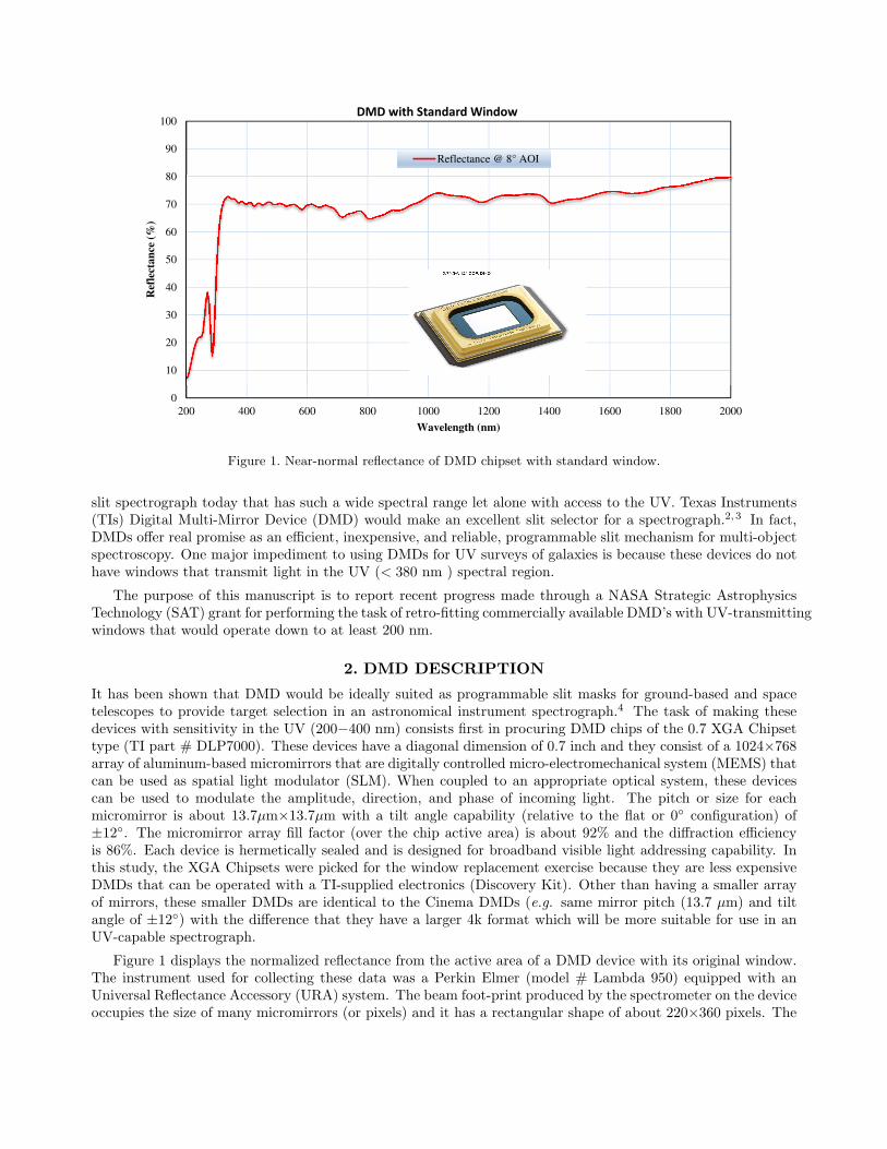
Figure 1. Near-normal reflectance of DMD chipset with standard window.
slit spectrograph today that has such a wide spectral range let alone with access to the UV. Texas Instruments(TIs) Digital Multi-Mirror Device (DMD) would make an excellent slit selector for a spectrograph.2,3 In fact,DMDs offer real promise as an efficient, inexpensive, and reliable, programmable slit mechanism for multi-objectspectroscopy. One major impediment to using DMDs for UV surveys of galaxies is because these devices do nothave windows that transmit light in the UV (< 380 nm ) spectral region.
The purpose of this manuscript is to report recent progress made through a NASA Strategic AstrophysicsTechnology (SAT) grant for performing the task of retro-fitting commercially available DMD’s with UV-transmittingwindows that would operate down to at least 200 nm.
2. DMD DESCRIPTION
It has been shown that DMD would be ideally suited as programmable slit masks for ground-based and spacetelescopes to provide target selection in an astronomical instrument spectrograph.4 The task of making thesedevices with sensitivity in the UV (200−400 nm) consists first in procuring DMD chips of the 0.7 XGA Chipsettype (TI part # DLP7000). These devices have a diagonal dimension of 0.7 inch and they consist of a 1024×768array of aluminum-based micromirrors that are digitally controlled micro-electromechanical system (MEMS) thatcan be used as spatial light modulator (SLM). When coupled to an appropriate optical system, these devicescan be used to modulate the amplitude, direction, and phase of incoming light. The pitch or size for eachmicromirror is about 13.7µm×13.7µm with a tilt angle capability (relative to the flat or 0◦ configuration) of±12◦. The micromirror array fill factor (over the chip active area) is about 92% and the diffraction efficiencyis 86%. Each device is hermetically sealed and is designed for broadband visible light addressing capability. Inthis study, the XGA Chipsets were picked for the window replacement exercise because they are less expensiveDMDs that can be operated with a TI-supplied electronics (Discovery Kit). Other than having a smaller arrayof mirrors, these smaller DMDs are identical to the Cinema DMDs (e.g. same mirror pitch (13.7 µm) and tiltangle of ±12◦) with the difference that they have a larger 4k format which will be more suitable for use in anUV-capable spectrograph.
Figure 1 displays the normalized reflectance from the active area of a DMD device with its original window.The instrument used for collecting these data was a Perkin Elmer (model # Lambda 950) equipped with anUniversal Reflectance Accessory (URA) system. The beam foot-print produced by the spectrometer on the deviceoccupies the size of many micromirrors (or pixels) and it has a rectangular shape of about 220×360 pixels. The

0
10
20
30
40
50
60
70
80
90
100
200 300 400 500 600 700 800 900 1000
Tra
nsm
itta
nce
(%
)
Wavelength (nm)
DMD Standard Window Transmission
Figure 2. Normal angle of incidence transmittance for a window substrate previously removed from a DMD chipset.
device was set in passive mode (i.e. without electronic control) with all the micromirrors in their default positions(tilt angle around 0◦). The angle of incidence (AOI) for these specular reflectance measurements was set at 8◦,which was relative to the vector perpendicular to the micromirrors surface in their default flat positions. Weobserve the average reflectance is around 73% over the 325−2000 nm range. This average reflectance representsthe absolute throughput of the device and it includes any losses from the intrinsic reflectance of each micromirror,the double pass through the window, and the fill factor (≈ 92%) of the micromirrors array. These data alsoshow a reflectance drop below 325 nm that is due to the window becoming opaque or absorbing for λ < 325 nm.The average reflectance below 325 nm is around 25% and it results from reflections of the window front-surfaceonly. This fact makes the DMD active area inaccessible below this wavelength. The only way to make theDMDs usable as a light modulation device in the UV spectral region is by replacing the existing windows witha UV-transmissive substrate. Section 3 below describes the window selection process for making UV-sensitiveDMDs.
3. UV-TRANSMISSIVE WINDOW SELECTION
3.1 Standard DMD Windows Characteristics
Current DMD windows assemblies are constructed of a Kovar (ASTM-F-15) metal alloy frame fitted with aborosilicate window substrate (Corning 7056). This type of glass has been chosen because it has good transmissionin the visible spectral range.5 In addition, the Corning 7056 glass has a coefficient of thermal expansion (CTE)that is very close to that of Kovar (Corning 7056: 5.15×10⁻⁶/◦C, vs. Kovar: 5.2×10⁻⁶/◦C.) This good match inCTE allows for a glass-to-metal hermetic seal when both are heated to nearly 1000 degrees Celsius. The hermeticseal is formed by heating both the glass and metal until a wetting of the metal by the glass occurs, followedby the development of a chemical bond or some mechanical interlocking, thus maintaining the seal. The basetransmission spectrum of Corning 7056 is nearly flat (≈ 93%) throughout the visible and near-infrared spectralranges. Figure 2 shows the transmission of a window that was previously removed from an existing DMD. Thetransmission shown in this figure indicates an average value close to 99% in the 400−700 nm range. These dataindicate this window has been treated with an anti-reflection (AR) coating for optimal transmission in the visiblerange. This figure also shows that a DMD suited with this window would have an average transmission of 68%between 300−400 nm, while the window is completely opaque (T ∼ 0) below 260 nm. Thus, the only way to

0
10
20
30
40
50
60
70
80
90
100
200 300 400 500 600 700 800
Tra
nsm
itta
nce
(%
)
Wavelength (nm)
Window Substrate Transmission
Magnesium Fluoride
UV-Grade FS
LAOS Sapphire
Figure 3. Transmittance at a normal angle of incidence for various UV-grade substrate options for DMD windows.
implement the DMD for application in a UV-capable spectrograph is to use a window optimized for maximumtransmission in the 200−400 nm range.
3.2 UV-Window Selection
As shown in Fig. 2, standard windows used on commercially available DMD will not pass light below 250 nm.This will preclude using these devices for application at wavelengths where the windows is required to have aslow absorption as possible. Fused silica is one of the most commonly used materials from deep-UV to mid-UVwavelength applications. Due to the polycrystalline nature of this material, its physical, thermal, dielectric andoptical properties are uniform and independent of crystallographic directions. The type of fused silica that wouldbe suitable for enabling UV application of DMD devices is termed excimer or UV-grade. Unfortunately, the CTEof UV-grade fused-silica (0.55×10⁻⁶/◦C) is roughly an order of magnitude smaller than that of Kovar. Thesedissimilar values in CTE will imply that as temperature would change during the post manufacturing process,the hermetic seal between the window and frame will not be maintained. A leaky seal will allow humidity in theenvironment to penetrate inside the device and this will become detrimental to the micromirrors inside causingthem not to function properly. One of the most common problems is that the mirrors would become sticky andcause them not to respond to commands.
Other window alternative with good transmission in the UV is magnesium fluoride (MgF2). This substrate isa low-index materials that transmits well into the vacuum ultraviolet (VUV) region at Lyman-Alpha (λ = 121.6nm). For this reason, this material has wide use in applications that span from the FUV to infrared wave-lengths. The crystallographic structure of MgF2 is tetragonal with a CTE that is anisotropic: 6.23×10⁻⁶/◦C and10.86×10−6/◦C in the directions perpendicular (⊥) and parallel (∥) to the c−axis respectively. The anisotropyin CTE will require that the crystallographic axes of the MgF2 would have to be chosen carefully so that theplane of the substrate is ⊥ to the c−axis given that the CTE in this perpendicular direction is a much closermatch to that of the Kovar frame.
A third option in window material for use in the UV is sapphire (Al2O3). The sapphire material, whichis considered a medium-index substrate, is widely used as an optical window material in the UV, visible, andnear infrared, mainly for its extreme toughness and strength. For this and other reasons, sapphire is also usedfor precision mechanical parts. Because of its hexagonal crystal structure, the CTE of crystalline sapphire isalso anisotropic: 7.0×10⁻⁶/◦C and 7.7×10⁻⁶/◦C in the perpendicular and parallel directions to the c−axis

0
2
4
6
8
10
12
14
16
18
20
200 220 240 260 280 300 320 340 360 380 400
Ref
lect
ance
(%
)
Wavelength (nm)
A/R Coating Performance (Per Surface)
Bare Sapphire
Bare MgF2
A/R Coated Sapphire
A/R Coated MgF2
Figure 4. Antireflection coating performance for sapphire and MgF2 substrates.
respectively. Hence, the optimum choice would be to use sapphire as an optical window that would have itsc−axis perpendicular to the plane of the substrate (because of the closer match to the Kobar CTE). A secondimportant consideration is the optical grade of the material. Standard grade sapphire would absorb light belowabout 260 nm. However, there is a low absorption optical sapphire (LAOS) material that is labeled VUV-grade.This type of sapphire combines high purity with extremely low defect density and special processing steps thatresults in a material that transmits light at wavelengths as low as 200 nm, where standard sapphire materialabsorbs the light. The VUV grade of sapphire is especially resistant to solarization and damage from radiationand the effects of long term immersion in high power UV light.
Figure 3 shows the transmission of the three substrate materials considered above as windows alternatives tothe DMD. The transmittance data shown in this figure indicate that any of the three substrate options discussedabove would be acceptable alternatives to replace the window so that the device would have a window with UV-transmission capabilities. The substrate with the highest transmittance is MgF2 (≈ 95%) on account of havingthe lowest refractive index of the three. The next substrate with the highest transmittance is UV-grade fusedsilica (90−93%), followed by LAOS sapphire (80−86%). It is obvious that the transmission of these windowswould have to be as high as possible in order to prevent any losses and, hence, maintain good efficiencies.Another reason is that any reflection, particularly on the inside of the window, can bounce back and forth fromthe inside of the window to the micromirrors to create “ghost images” that can cause interference problemswith the device. The solution is to coat both sides of the window with an AR coating that is optimized forthe intended wavelength range of use. Figure 4 displays the predicted performance on an AR coating appliedto the surfaces of sapphire and MgF2 substrates. The AR-coating design used to suppress reflection losses onboth of these substrates consists of two pairs of a high-index (GdF3) and low-index (MgF2) layer stacks withquarter-wave thicknesses that are optimized in the 200−400 range. Notice the reflection losses in both cases arebrought down to an average of less than 1%.
4. DMD REFLECTANCE
There is an additional consideration with respect to the use of DMDs as a programmable slit mask in the UVspectral range. It has to do with the intrinsic reflectance of the DMD active area. The commercially availableDMDs are made of micromirrors based on an aluminum (Al) alloy.6 To examine the intrinsic reflectance of themicromirrors, we removed the window and measured the specular reflectance of the bare device over the 200−2000

0
10
20
30
40
50
60
70
80
90
100
200 400 600 800 1000 1200 1400 1600 1800 2000
Ref
lect
ance
(%
)
Wavelength (nm)
Specular Reflectance vs. Time
0 month
1 month
4 months
13 months
Figure 5. Specular reflectance of one DMD as a function of time. The “0 month” trace corresponds to data takeninmediately after window removal.
0
10
20
30
40
50
60
70
80
90
100
200 400 600 800 1000 1200 1400 1600 1800 2000
Ref
lect
ance
(%
)
Wavelength (nm)
DMD Active Area Reflectance (No-window)
Pure Al
Device #1 (specular+diffused)
Device #2 (specular+diffused)
Device #1 (specular)
Device #2 (specular)
Figure 6. Specular and specular+diffused reflectance of two DMDs. The reflectance of pure Al is also shown for comparison.
nm range and using the same Perkin Elmer spectrometer fitted with the URA as described in Sec. 2. The resultsof these measurements are shown in Fig. 5. This figure shows the specular reflectance as a function of time (AOI= 8◦) after the window has been removed and the bare device has have been exposed to ambient conditions.We first observe that the reflectance does not show any degradation over a period of more than year. However,the absolute reflectance values appear much lower than what is expected from Al-based mirrors, particularlyfor wavelengths lower than 300 nm. In order to further quantify the reflectance properties of these DMDs, weshow in Fig. 6 the reflectance of two bare devices (to illustrate variability) along with the reflectance of a pureAl sample. The reflectance of the two DMDs (curves labeled as “specular”) is on average 35% lower than thatof the Al sample (for λ > 300 nm) and 20% lower for longer wavelenghts. Part of these reflectance losses couldbe accounted for by the filling factor (≈ 92%) due to the spaces or gaps between the micromirrors. These losses

0
10
20
30
40
50
60
70
80
90
100
200 400 600 800 1000 1200 1400 1600 1800 2000
Ref
lect
ance
(%
)
Wavelength (nm)
Specular+Diffused Reflectance Coated/Uncoated DMD
After Coating
Before Coating
Figure 7. Specular+diffused reflectance of DMD before and after an Al coating application of 59.5 nm.
would be realized by diffraction effects due to the periodic arrays of the micromirrors. In order to account forany losses due to these diffraction effects, we also performed Total Hemispherical Reflectance (THR), by usinga 60 mm integrating sphere accessory attached to the Perkin Elmer spectrometer. The THR measurementsinclude both specula plus diffused light that may be diffracted by the DMD arrays. The results of the traceslabeled ”specular+diffused” in Fig. 6 indicate that the THR is indeed higher than the ones corresponding to thespecular component alone. But even in this case, the THR data from these devices still do not match the resultsobtained from the pure Al sample. The overall reduced reflectance of the these devices (compared to Al) couldbe reasonably attributed to the fact that the Al in the DMDs may not be pure, but rather based on some typeof alloy. This could be inferred by the much lower reflectance (42% and 41% for Devices 1 and 2 respectively)at λ = 200 when compared to the reflectance of the pure Al sample.
4.1 Coating of DMD Active Area
The low reflectance of these DMDs below 300 nm (even when replacing the window with a substrate that hashigh transmittance in the UV spectral region) would severely limit the use of DMDs as programmable slit masksin a spectrograph with UV capability. One possibility to boost performance would be to coat the DMD activearea with a fresh Al layer. In order to determine the feasibility of such approach, we carried out a coatingtask of applying an Al layer with thickness between 50−60 nm on the Device #1 whose reflectance is shown inFig. 6. The first step in the process was to manufacture a mask with proper dimensions that would be placedon the front of the device during the coating process. This mask would have an aperture in the middle thatwould match the form factor (1024×768 pixels) of the device active area. The device would then be introducedinside a high-vacuum coating chamber where the Al deposition would take place. The Al coating process isbased on a Physical Vapor Deposition (PVD) method where the Al is placed in a resistive bowl (made out ofTungsten) with electrical wires attached to it. A current is passed through this bowl until the Al melts andevaporates onto the DMD inside the vacuum chamber. The device with the mask were placed directly on topof the bowl for the Al evaporation. One parameter that determines the quality of the deposited Al is a highvacuum (which was maintained from the low 10−7 Torr to the high 10−8 Torr range) during the coating process.We also ensured this vacuum chamber would have very low levels of residual water vapor and oxygen in orderto minimize the possibility of oxidation of the Al layer. The Al deposition rate was maintained at 100 A per

Figure 8. Setup for measuring reflectance of bare DMD.
second or higher, in order to obtain a denser Al film. Figure 7 displays the THR reflectance (specular+diffused)before and after Al was applied on the DMD active area. The coated device shows a substantial increase inreflectance reaching a value of 68% at 200 nm, when compared to the value prior to the coating application(42%). The results also show a more modest (4−5%) increase across the 400−2000 nm wavelength range, andthis may suggest the type of Al from which the micromirrors are made may contain some type of alloy thatexhibits a lower reflectance than that of pure Al. A topic of a future investigation will be to determine the effectof the evaporated Al on the functionality of the DMD. The main reason is because the deposited Al would go notonly on the micromirrors surface, but also has a small but distinct possibility of being deposited in-between themicromirror gaps and the surfaces behind them. The biggest risk from the Al deposition would be an electricalshort to the electromechanical mechanism that tilts each micromirror into the ±12◦ states.
4.2 DMD Scattering Properties
We will now discuss the scattering performance of the DMD micromirror arrays. These measurements weremade possible by using a Cary5000 spectrometer that is equipped with an Universal Measurement Accessory(UMA). The UMA defines two independent angular coordinate systems to describe the positions of the sampleand detector with respect to the incident light beam on the sample. The sample angle, which is defined as theangle between the direction of the incident beam and the direction perpendicular to the device surface, can befully driven from 0◦ through 360◦. On the other hand, the detector angle can be set in the range of 10◦−180◦
on either side of the incident beam. The specular reflectance of the sample is obtained when, for a given sampleangle θs, the detector angle is set at 2θs. Figure 8 shows how the DMD was configured inside the UMA samplecompartment. This figure shows the DMD is rotated in-plane by 45◦ so that the diagonals of each micromirrorare either in the horizontal or vertical directions. This figure also shows a sketch of the beam footprint the UMAproduces on the device active area that covers an area of approximately 320× 320 pixels or micromirrors. TheDMD was not powered up for these scattering measurements so the exact position of individual DMD mirrors isnot exactly determined and this uncertainty contributes to additional scattering. Figure 9 displays how the DMDreflectivity changes as the detector angle is varied from 10◦ through 90◦ along two directions within the plane ofthe DMD with the device AOI fixed at 20◦. This figure shows that, as expected, the DMD produces a mostlyspecular reflectance where the peak reflectance is reached at a detector angle of 40◦. Secondly, this figure showsa marked difference in the reflectance baseline (away from the specular component) when the detector is scannedalong two different orientations on the DMD (the curves labeled as “0◦” and “45◦”). It should be noted thatthe inset of Fig. 9 shows a strong diffraction pattern along the micromirror gap directions, which are along the±45◦ directions (relative to the horizontal or 0◦ orientation) in the image. As mentioned earlier, these diffraction

0.001
0.01
0.1
1
10
100
0 10 20 30 40 50 60 70 80 90
Refl
ecta
nce (
%)
Detector Angle (°)
Reflectance vs. Angle along 2 Orientations
45°
0° 0°
45°
Figure 9. Reflectance vs. angles for two orientations on the DMD. The inset in this figure illustrates the diffractionpattern along the (θ = ±45◦) directions when micromirrors diagonal is along horizontal (or vertical) directions. Noticethese diffraction patterns are formed when light illuminates the square arrays of micromirrors which are separated by agap of 0.6 µm.
1028
3644
5260
90
0
20
40
60
80
700600
500
400
300
200
Detector
Angle (°)
Re
fle
cta
nce
(%
)
Wavelength (nm)
DMD XGA Chip with Original Window
AOI= 20°
1028
3644
526090
0
20
40
60
80
700600
500
400
300
200Detector
Angle (°)
Re
fle
cta
nce
(%
)
Wavelength (nm)
DMD XGA Chip without window (Al-Coated)
AOI= 20°
Figure 10. Sample and detector angle definitions in the Cary5000+UMA system.
patterns are caused by the micromirror gap separation being in the order of visible or IR wavelengths (0.6 µm).Hence, the data shown in Fig. 9 indicates an 1−2 order of magnitude increase in the reflectance baseline whendetector is scanned along the diffraction pattern directions when compared to scanning along the horizontal (orvertical) directions that do not contain the diffraction pattern. Figure 10 displays two 3-dimensional plots of thereflectance as a function of detector angle and wavelength for the same device. The graph on the left shows thereflectance performance for the device with the standard (borosilicate) window, while the plot on the right showsthe reflectance performance of the same device after the window was removed and the DMD was coated with anAl layer as discussed in Sec. 4.1. These figures show more clearly the gains in reflectance that are realized after

the device has been coated with the Al layer.
5. CONCLUSIONS
In conclusion, we evaluated UV-transmitting windows made out of UV-grade fused silica, MgF2, and LAOSsapphire that could be used to replace standard borosilicate windows on commercially available DMDs in orderto enable these devices as programmable slit masks with UV capabilities. Secondly, we performed specular anddiffused reflectance on DMDs which had their windows removed in order to determine the throughput, durability,and scattering properties of the micromirrors reflective area. We found that although the reflectivity of baredevices was very stable and did not change over a period of more than year, the base reflectivity was low (≈ 58%over the 200−300 nm range). Because this reflectivity was lower than that of pure Al, we performed a coatingexperiment where the DMD active area of one device was coated with a fresh layer of pure Al (thickness = 59.5nm). We observed the average reflectance of the newly coated device increased to an average value of 75% in the200−300 spectral region. This boost in reflectance along with the replacement of the window with one of thethree substrate options mentioned above, will provide a viable path to use the DMD as a programmable slit maskin the UV spectral range. Future tasks will include verifying that Al-coated DMD will remain fully functionaland that no electrical short would occur due to the Al deposition on the electronic mechanism that provides the±12◦ micromirror tilt. Additional studies will also include a verification that adding this Al layer would notintroduce changes in the DMD wavefront surface figure error distortion that may be induced by changes in theflatness of the micromirrors array.
ACKNOWLEDGMENTS
This work has been performed in the Optics Branch (Code 551) at the Goddard Space Flight Center (GSFC)and supported through a NASA SAT grant No. NNX14AI62G. The authors wish to thank Linette Kolos andFelix Threat (NASA-GSFC/551) for their support in performing Al deposition on the bare DMD.
REFERENCES
[1] S. Jouvel, et.al.., “Designing future dark energy space missions. building realistic galaxy spectro-photometriccatalogs and their first applications,” Astronomy & Astrophysics 504, 359 (2009).
[2] Kearney, K. and Ninkov, Z., “Characterization of a digital micromirror device for use as an optical mask inimaging and spectroscopy,” in [Spatial Light Modulators ], Sutherland, R., ed., Proceedings of the Society ofPhoto-Optical Instrumentation Engineers (SPIE) 3292, 81–92 (1998).
[3] Fourspring, K., “Assessing the performance of digital micromirror devicestm for use in space-based multi-object spectrometers,” (2013).
[4] F. Zamkotsian, P. Lanzoni, E. Grassi, R. Barette, C. Fabron, K. Tangen, L. Valenziano, L. Marchand, L.Duvet, “Successful evaluation for space applications of the 2048x1080 dmd,” in [Emerging Digital MicromirrorDevice Based Systems and Applications III ], Douglass, M. R., ed., Proceedings of the Society of Photo-OpticalInstrumentation Engineers (SPIE) 7932, 79320A (2011).
[5] [Wavelenght Transmittance Considerations for DLP DMD Window ], Texas Instruments,http://www.ti.com/lit/an/dlpa031c/dlpa031c.pdf (May 2012-Revised March 2014).
[6] B.M. Callies, et.al., “Digital micromirror device having a window transparent to ultraviolet (uv) light,” U.S. Patent no: 7,161,727 B2 (2007).