open source for amateur radio projects including kicad pcb ... source for amateur radio projects_...
TRANSCRIPT

Open Source for Amateur Radio ProjectsIncluding Kicad PCB design
By Daniel Marks, KW4TIRaleigh Amateur Radio Society (rars.org)
September 10, 2019

What is “Open Source”?
It is a way to license software so that it remains “free.”
Free as in “beer,” you get free beer, you drink free beer, you don’t pay for it. Isn’t that great?
Free as in “libre,” the rights you receive as a software user, and guarantees as a developer.
• As a developer, your contributions to a free software project stay free (not made proprietary).
• As a user, your rights to use the software are irrevocable if you abide by the license.
• The source code is provided.• As a developer, your software is provided with no
warranty, and you are not liable for any damages.The licenses help developers and users cooperate.

Open Source in amateur radio:
It makes software and hardware tools available that help and encourage participation and enjoyment of the hobby.
(Highly incomplete list) examples of software:
• Fl-digi: amateur digital modes, (PSK31, etc.)• WSJT-X (FT8, JT65, etc.)• LOG4OM, cqrlog (logging software).• Dire Wolf terminal node controller software • CHIRP (program your transceiver).• NEC2 (antenna field solver) – 4NEC is non open
source but free front-end• Kicad (PCB design software).• Qucs (SPICE-based graphical circuit simulator)

Open Source Hardware in amateur radio:
Briefly, this means freely available schematics, PCBs, and firmware for hardware devices. Examples:
• uBitx/BITX 40 QRP transceiver• mcHF transceiver• EU1KY Antenna Analyzer• W8TEE Arduino Antenna Analyzer• Haasoscope USB digital oscilloscope• HPSDR (High Performance Software Defined
Radio) project (https://openhpsdr.org/)• HackRF One software defined radio• LimeSDR software defined radio
My own projects I will present today….

Developing your own ideas!
The tools of hardware and software development have never been as easy to use, cheaper, or more available as they are today. There are resources today that previous generations of hams could only dream about.

Did the Internet kill ham radio?
Quite the opposite. It provides the means for hams across the world to collaborate on projects. The benefits of these projects can be shared by all because the rights to the work are guaranteed by
Open Source Licenses.
But 21st century ham radio is going to be very different. Examples:
Complex digital modulation. (e.g. FT8/JT65)Smart Antennas. (e.g. phased array antennas)MIMO. Multiple input, multiple output antenna arrays.

Examples from my open source projects: a Vector Network Analyzer
A VNA is a device for measuring the reflections and transmissions from radio frequency components, for example, antennas and filters.
It can be used as an antenna analyzer, or to check the impedance of a balun, or the transmission of diplexer.
Can be built for under $50 in parts!

Examples from my open source projects: a linear power supply
This power supply allows one to make a new benchtop power supply from old, broken power linear power supply parts such as transformers, capacitors, and pass transistors.
This power supply has constant voltage and current capability and external control.

Examples from my open source projects: a Theremin
A microcontroller based Theremin, which is a musical instrument that can be played by moving one’s hands near the instrument’s antennas. Makes spooky sounds like in sci-fi movies.

Examples from my open source projects: an automatic antenna impedance matching unit
A do-it-yourself automatic antenna impedance matching unit that can be customized for various purposes, QRO, QRP, or for antenna experimentation.

New PCB manufacturing services make obtaining custom PCBs for your project very cheap!
PCB manufacturers such as JLCPCB, Seeedstudio, and PCBway can manufacture two-layer PCBs up to 10-by-10 cm for $5 or even less!
This can take the chore of handwiring together electronic components on a breadboard, and make it much easier and neater. They can also populate boards for you as well.
Today, I’m going to walk you through how to create a PCB with Kicad and submit it to one of these services.

Simple Kicad project: 555 LED flasher circuit
555Timer
4Reset
8Vcc
1 Gnd5 Control
0.01 mF
2 Trigger6 Threshold
C
7 Discharge
R2
R1
3Output
R3
D

Starting a project
Create a directory for your project (for example “FlashLED”) and then place the project file “.pro” into that directory

The project is started. Now what?
File with your captured schematic
File with your PCB layout
Schematic editor
Parts symbol editor
PCB Layout
Footprint editor
Gerber viewer
First: capture schematic (schematic editor)

Empty schematic. Lets add some parts!

Place a component
Then click on the location on the schematic you want the component placed with the crosshairs.
Type “555” to search the loaded libraries. Kicad lists the components with part numbers that match the search term.

Move the part with the mouse cursor and click where the part should be placed.
Now the part is placed.

Assign a footprint
The footprint tells Kicad how to place the pads so that the selected part can be soldered into the board. For example, the NE555 chip has a DIP-8 package. To select the footprint, right-click on the part and then
Click Select to choose the footprint

Library with footprint
Selected footprint in library

Footprint field now shows selected footprint
Click ok
Now you’ve placed your first part!

Placing a ¼ watt resistor
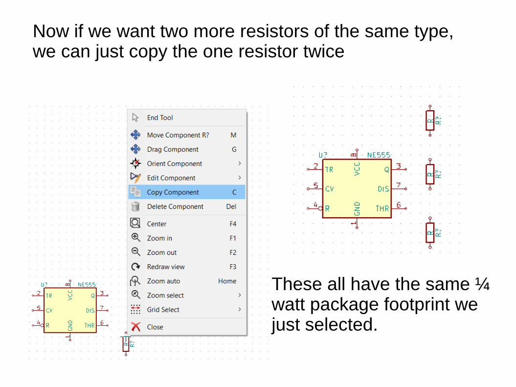
Now if we want two more resistors of the same type, we can just copy the one resistor twice
These all have the same ¼ watt package footprint we just selected.

Placing a small ceramic disc capacitor

Placing a radial polarized capacitor

Placing a 5 mm LED

What we have so far...
What else do we need?
POWER!
To do this we need power ports.
We choose the place power port menu item.

We can expand the list of power ports and select 6 volts, for example, for the positive voltage.
Then we can place a second power port for ground.

Now we have power ports. Finally, we need a way to connect external wires to the power port, so we place screw terminals.
Placing a two terminal connector
Footprint for standard 2/10” spacing screw terminals.

Wiring it all up
First move and rotate the components into the approximate right places. Right click on part and select move or rotate component.

Now we can draw wires between the components
Click where you want wires to begin or end. You can placed bends in wires by clicking on points you want the wire to bend at.
If you right-click on a wire, you can remove the connection.

Schematic capture is complete!

Schematic capture is complete!
Now we export a netlist, which provides the PCB layout editor the description of the schematic.
We select the name of the netlist file to save to (usually the default).

Annotating the schematic references
Since we didn’t specify what the part references were (for example R1, R2, R3 for the three resistors), and these are required for the PCB editor, Kicad will automatically annotate the references. These may be assigned manually if desired as well when you create the part.

Now the references are added to the schematic.
On with laying out the PCB!

PCB Layout
PCB Editor

Importing the netlist into the PCB editor
Click Read Current Netlist
All of the components are imported, and lines drawn between the pins to be connected.

Moving the components
Lets move the parts so they’re not on top of each other so we can better see what we’re doing.
Kicad shows us how the parts are to be connected, but these are not wires. This is called the “ratsnest.”
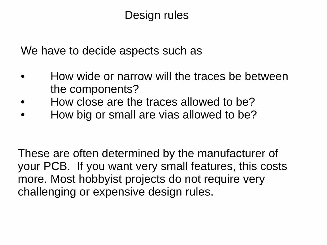
Design rules
We have to decide aspects such as
• How wide or narrow will the traces be between the components?
• How close are the traces allowed to be?• How big or small are vias allowed to be?
These are often determined by the manufacturer of your PCB. If you want very small features, this costs more. Most hobbyist projects do not require very challenging or expensive design rules.

Setting the design rules
These rules determine via sizes and minimum feature sizes and widths.
These are the widths of the tracks that can be placed. 0.5 mm is placed here.

Commonly used board Layers
Front copper layer (where traces go on the front of the board)
Back copper layer (where traces go on the back of the board)
Front silkscreening layer, so you can annotate your PCB
Edge Cuts (not used by all manufacturers), denotes the boundaries of your PCB (usually a rectangle)
Front and back solder mask.

Drawing the traces between components
We move and rotate the components into position. To draw a trace between two pads, we first select the trace size:
Select the layer the trace goes on by clicking on the layer name. The arrow appears next to the selected layer.
Then we select the draw track tool.

Connecting the components
The ratsnest tells us which components to connect. Kicad will not allow us to make connections not in the ratsnest, as these are not compatible with the schematic.
Pick this connection
Click on one of the ends of the ratsnest, and guide the trace to the other end, and click the other end.
The ratsnest line is replaced by a trace with the color given by the layer.

Filling in all of the traces
Each trace is labeled by its “net name” which describes which pads it connects.
We can add silkscreening
Selectsilkscreen
layer
Texttool

Adding silkscreening
Click on the PCB where you want to add the silkscreening and then type the text into the box:

Drawing the board outline
Selectedge cuts
layer
Choose line tool
Select a coarse grid size to make it easier to draw a straight rectangle

With the board outline
Now we do a design rules check to make sure everything is ok!
Do design rule check

Design rule check success!
Problems can be parts are too close together or touching that should not be, too small width between traces, etc. If you click on the problem it takes you the location of the PCB.

What does my PCB look like?
Use the 3-D viewer

Exporting the Gerber files
Gerber files are what you send the PCB manufacturer to make your PCB.
Select plot from the menu
Check these layers, which are typically what is needed (unless you need a solder stencil as well)
Enter “gerber” here so the files are in a separate directory.
Click “plot” to generate the gerbers

Exporting the Excellon Drill Files
You also need files to indicate the holes to drill.
Click here to generate drill files.
The drill files go into the same directory as the gerber files.

Sending your job to be manufactured (example, JLCPCB)
We zip up the gerber directory into a single file
Use your favorite zip program (I use 7-zip under Windows)
Now we have a zip file of the “gerber” directory.

Log onto JLCPCB website (www.jlcpcb.com)
Click “quote now.”
Click “add your gerber file.”
Find and upload the gerber zip file.

And here it is, you can see the front and back of the PCB board in the on-line viewer.
Use the “Gerber Viewer” link to check to make sure JLCPCB’s system is reading your gerber files correctly.

Finish filling out the form and complete the order.
And that is an example on how to design a PCB with Kicad and have it made, start-to-finish!
Designing library symbols and footprints are important tasks, but not covered here.
Also adding copper fills and vias are not covered in PCB layout, also important.

Some examples:
PowerSupplyPCB
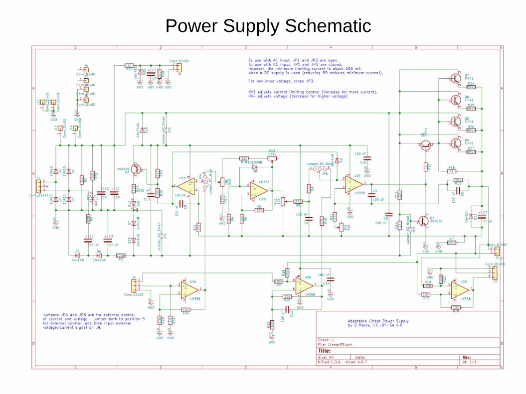
Power Supply Schematic

Some examples: VNA PCB

Conclusions
Hams across the world work together on open source projects that are freely shared by all.
If you have an idea, go for it! Open-source tools like Kicad are out there to be used by people like you.
If you like a project, participate! Be a user, document something, make a instructional video, or even design a circuit or write some code.
Kicad is available at www.kicad-pcb.org
My projects are available on http://www.github.com/profdc9/