onthedevelopmentofhighpowerdc-dcstep...
TRANSCRIPT

Hindawi Publishing CorporationAdvances in Power ElectronicsVolume 2012, Article ID 806738, 10 pagesdoi:10.1155/2012/806738
Research Article
On the Development of High Power DC-DC Step-Down Converterwith Energy Recovery Snubber
Alok Singh, Mangesh B. Borage, Sunil R. Tiwari, and A. C. Thakurta
Power Supplies and Industrial Accelerator Division, Raja Ramanna Centre for Advanced Technology,Indore 452013, India
Correspondence should be addressed to Alok Singh, [email protected]
Received 27 December 2011; Revised 28 March 2012; Accepted 29 March 2012
Academic Editor: Jose Pomilio
Copyright © 2012 Alok Singh et al. This is an open access article distributed under the Creative Commons Attribution License,which permits unrestricted use, distribution, and reproduction in any medium, provided the original work is properly cited.
The effect of switching losses on the efficiency of a switch mode power converter and methods adopted for its improvement usingan energy recovery lossless snubber has been presented. A comparative analysis of various types of soft switching techniques alongwith effects of dissipative and nondissipative snubbers on efficiency of the converter has been carried out before zeroing in onthe selected scheme. The selected snubber serves the dual function of a turn-on and turn-off snubber and thereby reducing theswitching losses both during turn-on and turn-off transients, resulting in improved efficiency of the converter. A detailed designprocedure of the snubber for high-power applications taking into account various effects such as diode reverse recovery, diodevoltage stress, and minimum and maximum duty cycle limits, has been presented in this paper. Importance of practical aspectsin layout to minimize wiring inductance is also highlighted. A high-power prototype of buck converter has been developed toexperimentally validate the theoretical design and analytical observations.
1. Introduction
Switch mode power supplies are popular because of higherefficiency, smaller size, and lighter weight [1, 2]. Lowweight and smaller size comes about because operationis significantly at a higher frequency range, and thus themagnetic components are quite smaller in size and weight[3]. High switching frequencies in turn results in largeswitching losses and stresses in power device because duringthe turn-on and turn-off transients the power device has towithstand high voltage and current simultaneously [4, 5].Large di/dt and dv/dt transitions also induces significantamount of electromagnetic interference (EMI) in the circuitwhich in turn pollute the utility systems [6]. This problem,if left unattended, may result in lower efficiency and largersize of converters owing to increased size of the heat sinksand EMI filters. Efforts are made in order to alleviatethe aforementioned limitations and to enable operation atstill higher frequencies while maintaining better conversionefficiency [7].
Snubbers are an essential part of power electronicsystems. They are small network of passive components
which forms a part of power switching circuits to reduceswitching losses and stresses in power devices [8]. But, asthe switching losses in the main switch are dissipated inform of heat in snubber resistors, the overall efficiency of theconverter is deteriorated. Various soft switching techniqueshave been proposed in the literature [1, 9, 10] to obtainsoft switching of power devices while at the same timemaintaining higher overall efficiency. But this is achieved atthe cost of increased design complexity of power and controlcircuits and thereby increasing circuit cost and deterioratingthe system reliability [5].
Energy recovery snubber poses a solution to the problemas it is simpler, reliable, and cheaper than most of thesoft switching techniques and also helps in reducing theswitching losses without deteriorating the overall systemefficiency. The energy stored in an energy recovery snubberis either moved back to the input or ahead to the output ina nondissipative manner [5, 6, 8, 11, 12]. Energy recoverysnubbers can be further classified as turn-on, turn-off, andcombined function snubbers. Turn-on snubbers are basicallynondissipative current snubbers which control the rate of

2 Advances in Power Electronics
Vd
S1
Cs
Cb
Ls
Lm
Co
Rd
Vo
+
−Snubber cell
R
+−
Cd
D4
D3
D2
D1
Figure 1: Buck converter with energy recovery snubber.
rise of current in the main switch at turn-on transient andthereby achieving zero current switching (ZCS) at turn-ontransient of the switch [8, 13], while turn-off snubbers arenondissipative voltage snubbers which control growth rateof voltage across the switch during turn-off transient andthus help in achieving zero voltage switching (ZVS) at turn-off transient [8, 14–17]. The combined function snubber,also called as turn-on and turn-off snubber, serves the dualfunction of achieving ZCS turn-on and ZVS turn-off of theswitch during turn-on and turn-off transients, respectively,and hence includes the functionality of both turn-on andturn-off snubber in a single circuit [5]. An energy recoveryturn-on and turn-off snubber is thus selected for furtherinvestigation and implementation in a high power dc-dcconverter.
Although, synthesis and optimization of various snub-bers have been widely reported in the literature for lowpower dc-dc converters [1, 5, 6, 9–19], the issues relatedto design, optimization, application, and practical aspectspertaining to their use in high power dc-dc converters are notreported. This paper presents the design and optimizationof energy recovery snubber with wide operating range forhigh power dc-dc converters. The presented work is based onthe analytical results reported in [5]. Brief operation of theenergy recovery snubber is presented in Section 2 followed bydesign parameters of dc-dc converter in Section 3, design andoptimization of energy recovery snubber in Section 4, simu-lation and experimental results in Section 5, and conclusionsin Section 6.
2. Operation of Energy Recovery Snubber
Snubber shown in Figure 1 is an energy recovery turn-onplus turn-off snubber also called as 3D-2C-1L snubber. Thesnubber network has been called so because it has threediodes, two capacitors, and one inductor. Growth rate ofreverse recovery current is controlled by snubber inductorLs, while growth rate of voltage across switch is controlledby snubber capacitor Cs. Energy recovery is achieved bydischarging the buffer capacitor Cb to the output. Thekey waveforms of the buck converter with energy recoverysnubber are shown in Figure 2 [5]. During turn-on process,the diode recovery current is the major cause of the switchinglosses and EMI. The rate of rise of current and peak reverserecovery current is restricted by the snubber inductor Ls to
Table 1: Prototype specifications.
Maximum output power 25 kW
Switching frequency 25 kHz
Filter inductor, Lm 800 μH
Filter capacitor, Co 3 μF
Filter damping capacitor, Cd 15 μF
Filter damping resistor, Rd 15Ω
suppress the switching loss. During turn-off process, the rateof rise of drain-source voltage is restricted by the snubbercapacitor Cs to obtain ZVS turn off and to reduce EMI noises.
The freewheeling diode is also commutated with ZVSduring both turn-on and turn-off. The energy absorbed insnubber inductor Ls and snubber capacitor Cs is transferredto Cb instead of being dissipated, which is subsequentlytransferred to the output. Detailed operation of this snubberwith various modes of operation is given in [5].
3. Design Parameters of DC-DC Converter
A high-power prototype of buck converter with maximumoutput voltage and current ratings of 450 V and 55.5 A,respectively, has been developed to experimentally validatethe theoretical design of energy recovery snubber. The designparameters of the buck converter are given in Table 1.
The insulated gate bipolar transistor (IGBT) moduleused in the prototype is SKM100GAR123D [20].
4. Design and Optimization ofEnergy Recovery Snubber
Design and optimization of energy recovery snubber aredescribed in six steps as given below. Subsequently, a designflow diagram for snubber parameters calculation is alsopresented in Figure 3.
Step 1 (Choice of Cs). The snubber capacitor Cs shown inFigure 1 is mainly responsible for ZVS turn-off of switch S1.Thus, the discharging time of Cs should be quite larger thanthe fall time t f of the switch to ensure proper ZVS turn-off of the switch. When the switch S1 turns off, the outputcurrent Io flows through D2 to discharge Cs to the output.

Advances in Power Electronics 3
Vg
t0 t1 t2 t3 t4 t5 t6 t7 t8
Time
Io
Vd
Vd
Io
Io
Io
Vd
(Vd + VCb,p)
ILs
VCs
VCb
(Io + ILs,p)Vs
Is
VD1
ID2
ID3
ID4
ID1
Figure 2: Key waveforms of the buck converter with energy recovery snubber.
During this period, capacitor discharges linearly. If the timetaken by Cs to discharge completely from the value of Vd tozero is td, then, capacitance Cs can be written in terms ofoutput current Io, input dc voltage Vd and discharge time tdas follows:
Cs = IotdVd
. (1)
As typically the fall time t f of the switch is around100 ns. Thus, to ensure proper ZVS turn-off of the switch,discharge time td is taken to be approximately five-times thefall time of switch t f , that is, 500 ns. Therefore, for (Io)max
= 55.55 A, (Vd)min= 504 V, and td = 500 ns, the value ofsnubber capacitance Cs comes out to be 0.055 μF from (1).The nearest available value of snubber capacitance used inthe practical circuit is 0.047 μF.
Step 2 (Choice of Ls). When the switch S1 shown in Figure 1is turned on, the growth rate of the drain current is restrictedby the snubber inductor to softly turn on the switch. Duringthis duration, rate of fall of main diode current iD1, which
is also equal to the rate of rise of switch current, is given asfollows:
diD1
dt= Vd
Ls. (2)
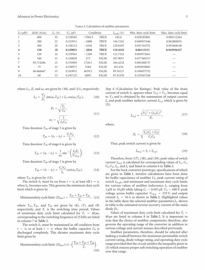
Values of diD1/dt calculated for various values of Ls andVd = 600 V using (2) have been listed in column 2 in Table 2.Column 3 in Table 2 shows the estimated values of reverserecovery current Irr flowing through main diode D1 for thecorresponding values of diD1/dt listed in column 2. Thesevalues have been estimated from Irr v/s diD f /dt curve givenin the datasheet of IGBT module [20].
Step 3 (Choice of Cb). Buffer capacitance Cb is expressed interms of Ls, Cs, Vd, Irr, and VCb,p as follows [5]:
Cb = LsIrr2 + CsVd
2
VCb,p2 . (3)
As the voltage stress of freewheeling diode D1 is equal toVd plus VCb,p, thus the peak voltage appearing across buffercapacitor Cb is capped at 235 V to keep the voltage rating

4 Advances in Power Electronics
Start
Calculate Cs using (1)
of IGBT module
Calculate Cb for corresponding
using (3)
Calculate LHS of conditiongiven in (5)
Stop
Increment Ls
No
No
No
Yes
Yes
Yes
Whether Dmin
and Dmax arewithin limits
Calculate Dmin and Dmax from
Calculate Isw,p from (21)
Whether Isw,p
is withinlimits
condition < 0
Estimate Irr for corresponding
values of Ls,Cs, Irr, and Vcb,p
(17) and (18), respectively.
Finalize values of Ls,Cs, and Cb
Is
Choose a value of Ls andcalculate diD1/dt using (2)
value of diD1/dt from datasheet
Figure 3: Design flow diagram for snubber parameters calculation.
of D1 within limits (maximum voltage rating of diode D1 is1200 V). Hence, the peak voltage appearing across diode D1
is given by.
VD1,p = Vd + VCb,p∼= 850 V. (4)
Thus, values of Cb calculated for corresponding values ofLs, Cs, Vd, Irr, and VCb,p are listed in column 4 in Table 2.
Step 4 (Checking for Condition). The necessary conditionwhich ensures the proper ZCS turn-on and ZVS turn-offoperation of circuit is given in [5] and can also be writtenas follows:
12LsIo
2 − 12LsIrr
2 − 12CsVd
2 < 0. (5)
Column 5 in Table 2 calculates the left hand side (LHS)of inequality given in (5) and the result is TRUE if LHS isnegative, while FALSE otherwise.
Step 5 (Check for Dmin and Dmax). Maximum and minimumduty cycle limits are imposed on the buck converter due tofinite time taken by the snubber circuit for its operation. Dur-ing this duration, the normal operation of buck converteris suspended. Maximum duty cycle limit occurs due to thesnubber circuit operation at switch turn-off transition, whileminimum duty cycle limit occurs due to the snubber circuitoperation at switch turn-on transition. Thus, the duty cyclelimits can be obtained by calculating the time taken by thesnubber both during turn-on and turn-off transitions.
Various stages of operations have been discussed in[5]. Out of 8 stages of operation of buck converter circuitdescribed in [5], snubber is active during 6 stages (t0 < t <t1), (t1 < t < t2), (t2 < t < t3), (t4 < t < t5), (t5 < t <t6), and (t6 < t < t7). Time duration of all these 6 stagesare calculated here for values of Ls varying from 1 μH to10 μH, Cs = 0.047μF, Vd = 600 V, peak voltage across buffercapacitor VCb,p = 235 V, and output current Io = 56 A. Todo this, expressions for time durations for these stages arederived based on equations describing voltages and currentsgiven in [5]. They are summarized as follows.
Time duration Td1 of stage 1 is given by
Td1 = (t1 − t0) = LsVd
(Io + Irr). (6)
Time duration Td2 of stage 2 is given by
Td2 = (t2 − t1)
= 1ω1
⎧⎪⎨
⎪⎩sin−1
⎛
⎝CsVd
Cb
√
(IrrZ1)2 + Vd2
⎞
⎠ + tan−1 Vd
IrrZ1
⎫⎪⎬
⎪⎭,
(7)
where Z1 and ω1 are given in (8),
Z1 =√
Ls(Cs + Cb)CsCb
,
ω1 =√
Cs + Cb
LsCsCb.
(8)
Time duration Td3 of stage 3 is given by
Td3 = (t3 − t2) = 1ω2
tan−1(CbIs2Z2
CsVd
)
, (9)
Advances in Power Electronics 5
Table 2: Calculation of snubber parameters.
Ls (μH) di/dt (A/us) Irr (A) Cb (μF) Condition Isw,pk (A) Min. duty cycle limit Max. duty cycle limit
1 600 35 0.328565 −7504.5 TRUE 182.6 0.028185861 0.969112264
2 300 22 0.323911 −5808 TRUE 144.7242 0.040937446 0.962884825
3 200 20 0.328112 −4356 TRUE 129.0297 0.051743372 0.955668148
4 150 18 0.329851 −2836 TRUE 119.4543 0.06115151 0.945936337
5 120 16 0.329561 −1260 TRUE 112.7242 0.069572661 —
6 100 15 0.330828 273 FALSE 107.9057 0.077569317 —
7 85.714286 15 0.334903 1728.5 FALSE 104.4218 0.085468737 —
8 75 15 0.338977 3184 FALSE 101.634 0.093078882 —
9 66.666667 15 0.343051 4639.5 FALSE 99.34127 0.100457752 —
10 60 15 0.347125 6095 FALSE 97.41529 0.107647168 —
where Is2, Z2 and ω2 are given by (10), and (11), respectively:
Is2 = Vd
Z1sin(ω1Td2) + Irr cos(ω1Td2), (10)
Z2 =√
LsCb
,
ω2 =√
1LsCb
.
(11)
Time duration Td4 of stage 5 is given by
Td4 = (t5 − t4) = CsVd
Io. (12)
Time duration Td5 of stage 6 is given by
Td5 = (t6 − t5) = 1ω2
sin−1
(IoZ2
VCb,p
)
. (13)
Time duration Td6 of stage 7 is given by
Td6 = (t7 − t6) = CsVd
Iocos(ω2Td5), (14)
where Td5 is given by (13).The switch S1 must be on from t = t0 at least till t = t3
when ILs becomes zero. This governs the minimum duty cyclelimit which is given by
Minimumduty cycle limit (Dmin) = Td1 + Td2 + Td3
Ts, (15)
where Td1,Td2, and Td3 are given by (6), (7), and (9)respectively, and Ts is the switching time period. Valuesof minimum duty cycle limit calculated for Ts = 40μs,corresponding to the switching frequency of 25 kHz are listedin column 7 in Table 2.
The switch S1 must be maintained in off condition fromt = t4 to at least t = t7 when the buffer capacitor Cb isdischarged completely. This dictates maximum duty cyclelimit given by
Maximumduty cycle limit (Dmax)=1−(Td4 + Td5 + Td6
Ts
)
.
(16)
Step 6 (Calculation for Ratings). Peak value of the draincurrent of switch S1 appears when VCb + VCs becomes equalto Vd and is obtained by the summation of output currentIo and peak snubber inductor current ILs,p which is given by[5]:
ILs,p =√
Vd2 + (IrrZ1)2
Z1, (17)
where,
Z1 =√
Ls(Cs + Cb)CsCb
. (18)
Thus, peak switch current is given by
Isw,p = Io + ILs,p. (19)
Therefore, from (17), (18), and (19), peak value of switchcurrent Isw,p is calculated for corresponding values of Ls, Cs,Cb,Vd, Irr, and Io and listed in column 6 in Table 2.
For the buck converter prototype, specifications of whichare given in Table 1, iterative calculations have been donefor buffer capacitance of snubber Cb, peak current rating ofswitch Isw,pk, and minimum and maximum duty cycle limitsfor various values of snubber inductance Ls ranging from1 μH to 10 μH while taking Cs = 0.047μF, Vd = 600 V, peakvoltage across buffer capacitor VCb,p = 235 V, and outputcurrent Io = 56 A as shown in Table 2. Highlighted valuesin the table show the selected snubber parameters.Irr shownin table is the estimated reverse recovery current of the maindiode D1.
Values of maximum duty cycle limit calculated for Ts =40μs are listed in column 8 in Table 2. It is important tonote that the choice of snubber components, therefore, alsogoverns the operating range of the converter in addition tovarious voltage and current stresses described previously.
Snubber parameters, therefore, should be selected aftermaking a tradeoff between the maximum permissible switchcurrent rating, diode voltage rating, and operating duty cyclerange provided that the circuit satisfies the inequality given in(5) which ensures proper soft switching operation of snubberover that range.

6 Advances in Power Electronics
600
400
200
0
Switch voltage Switch current
478.4 479.2 480 480.8 481.6 482.4
Time (µs)
IC(Z2)∗5V(Z2: C,D16: 2)
Figure 4: ZCS turn-on of switch S1.
699
600
400
200
0
470.8 471.6 472.4 473.2 474 474.8
Switch voltageSwitch current
Time (µs)
IC(Z2)∗5V(V2: +, D16: 2)
Figure 5: ZVS turn-off of switch S1.
Based on the calculations illustrated in Table 2, thefollowing component values are chosen:
Ls = 4μH,
Cs = 0.047μF,
Cb = 0.33μF,
Isw,p = 119.45 A,
VD1,p = 850 V,
VCs,p = 616 V, ICs,p = 55.5 A, and
VCb,p = 235 V, ICb,p = 55.5 A.
Diodes APT60D100B are used for snubber diodes [21].Inductor Ls is developed in EE65.32.18 core with 4 turns andan air gap of 1.4 mm.
5. Simulation and Experimental Results
Simulation results for voltage and current waveforms acrossswitch in the presence of energy recovery snubber are shownin Figures 4 and 5, respectively, during on-time and off-timetransitions for input dc voltage, Vd = 616 V and outputcurrent, Io = 56 A. From Figures 4 and 5, respectively, itis observed that energy recovery snubber helps in achievingZCS turn-on and ZVS turn-off of switch S1 at turn-on andturn-off transients.
1
0.95
0.9
0.85
Dissipative snubber
Without snubber
Nondissipative snubber
0.1 0.2 0.3 0.4 0.5 0.6 0.7 0.8 0.9
Figure 6: Efficiency comparison of buck converter with dissipativeand nondissipative snubbers.
Simulation results for comparison of efficiency of buckconverter with and without dissipative and nondissipativesnubbers are shown in Figure 6 in which x-axis representsduty cycle variation from 0.1 to 0.9, while y-axis representsefficiency of buck converter. Dissipative snubber used insimulation consists of two cells one of which is responsiblefor achieving ZCS turn-on of the switch, while the otherone ensures its ZVS turn-off. The turn-on snubber cell isplaced in series with the switch and consists of an inductor(4 μH) connected in parallel with the series combination of aresistor (5Ω) and an ideal diode. While the turn-off snubbercell is placed across the switch and consists of a capacitor(0.047 μF) placed in series with a parallel combination of aresistor (68Ω) and an ideal diode. Nondissipative snubbercomponents used in simulation are same as summarizedin Section 4. From Figure 6 it is observed that efficiency ofthe buck converter reduces when a dissipative snubber isused to limit the switching losses. This is because of thefact that in dissipative snubbers switching losses in powerdevices are transferred to the dissipative component in thesnubber thereby reducing overall efficiency of the converter.But, in contrast to this, nondissipative snubber reducesthe switching losses by temporarily storing the energy ofone switching transient in a buffer and then transferringit either back to the input or ahead to the output duringthe next switching transient in a nondissipative manner andthereby, reducing the switching losses while at the same timeincreasing the efficiency of the converter. The improvementin efficiency with energy recovery snubber is evident insimulation waveforms of Figure 6.
The simulation waveforms shown in Figures 4 and 5are valid only for ideal circuits which are free of anywiring inductances. But, in practical circuits, these wiringinductances play a significant role in introducing undesirableeffects on the circuit operation. This can be demonstratedby introducing some wiring inductance in series with theinput dc supply of simulation circuit. Figure 7 shows thesimulation waveforms with the effects of wiring inductanceof 100 nH introduced in the simulation circuit.
From Figure 7, it is observed that the wiring inductanceshave significant undesirable effect on the circuit perfor-mance. During turn-off transition, ringing is observed inswitch voltage and current waveforms which results in anoverlap between the two during the transition interval andthereby resulting in switching loss at turn-off transition

Advances in Power Electronics 7
(V)
1.87085 1.872 1.874 1.876 1.878 1.88 1.882
Time (ms)
Gate pulse1510
50
V(V4: +, V4: −)
(a)
1.87085 1.872 1.874 1.876 1.878 1.88 1.882
750500
−50SEL≫
Time (ms)
Switch voltage and currentWiring inductance effect
voltageWiring inductance effect
current
V(Z2: C, Z2: E)
IC(Z2)∗5
(b)
1.87085 1.872 1.874 1.876 1.878 1.88 1.882
Time (ms)
voltagecurrent
Main diode voltage and current
0
1000500
−500
I(D19)∗14
V(D19: 2,D19: 1)
(c)
1.87085 1.872 1.874 1.876 1.878 1.88 1.882
Time (ms)
(A) 50
0−50
Inductor current
I(L3)
(d)
Figure 7: Simulation waveforms with effect of wiring inductance for D = 0.5, Vd= 616 V, and Io = 56 A: gate pulses, voltage and current inS1, voltage and current in D1, and current in Ls.
vge−s1
vs1
is1
(a)
vge−s1
vs1
is1
(b)
Figure 8: Experimental waveforms of vs1 (50 V/div) and is1 (10 A/div) at (a) turn-on transition and (b) turn-off transition. In both parts,Ch3 shows gate pulse for switches (vge−s1, 20 V/div) and XScale is 250 ns/div.

8 Advances in Power Electronics
vge−s1
iLs
vD1
(a)
vge−s1
iLs
vD1
(b)
Figure 9: Experimental waveforms of vD1 (50 V/div) and iLs(10 A/div) at (a) diode turn-on transition and (b) diode turn-offtransition. In both parts, Ch3 shows gate pulse for switches (vge−s1,20 V/div) and XScale is 500 ns/div.
as shown in Figure 7. Ringing is also observed in switchcurrent after turn-on transition which disrupts the normalfunctioning of the buck converter during this interval asshown in Figure 7. Thus, significant steps should be takenduring the development phase of the converter to minimizethese wiring inductances by making a judicious arrangementfor the assembly of snubber and other components ofthe converter. This can be done by prudently placing thecomponents containing high frequency currents as close toeach other as possible and thereby minimizing the wiringlength which in turn results in reduced wiring inductance.Another way to reduce wiring inductance is to use twistedcables or to use flat wide conductors and using copper strips.
Figures 8(a) and 8(b) shows the experimental waveformsof the voltage across the switch (vs1) and current throughit (is1) at turn on and turn off transitions, respectively, forD = 0.5 and Vd = 200 V. From Figure 8, it is clear that theswitch turns on under ZCS condition and turns off underZVS condition which is in agreement with the theoretical
vge−s1
iLs
(a)
iLm
vge−s1
vD1
(b)
Figure 10: Experimental waveforms of (a) iLs (10 A/div) withXScale of 5 μs/div and (b) vD1(50 V/div), iLm(5 A/div) with XScaleof 10 μs/div. In both parts, Ch3 shows gate pulse for switches (vge−s1,20 V/div).
analysis of switch voltage and current waveforms and alsowith the simulation results presented in Figure 7.
Figures 9(a) and 9(b) shows the experimental waveformsof main diode D1 voltage(vD1)and snubber inductor Lscurrent (iLs) at turn on and turn off transitions respectivelyfor D = 0.5 and Vd = 200 V.
Since snubber inductor Ls is connected in series withthe main diode D1, as shown in Figure 1, a part of snubberinductor current flows through main diode D1 both duringturn-on and turn-off transitions. As, it is difficult to monitorcurrent waveform in main diode, snubber inductor currentis observed here to demonstrate the ZVS turn-on and ZVSturn-off of the main diode D1. From Figure 9, it is clear thatthe main diode D1 also turns-on and turns-off under ZVScondition which is in agreement with the theoretical analysisof main diode voltage and current waveforms and also withthe simulation results presented in Figure 7.
Figure 10(a) shows the snubber inductor Ls currentwaveform for full cycle of operation while Figure 10(b) shows

Advances in Power Electronics 9
0.5
0.55
0.6
0.65
0.7
0.75
0.8
0.85
0.9
0.95
1
0.2 0.3 0.4 0.5 0.6 0.7 0.8 0.9
Effi
cien
cy
With snubberWithout snubber
Duty ratio
Figure 11: Measured efficiency of buck converter with and withoutnondissipative snubber at Vd = 100 V.
the voltage and current waveforms of main diode D1 andoutput filter inductor Lm, as shown in Figure 1, respectivelyfor D = 0.5 and Vd = 200 V. Figure 10(a) demonstratesthat the snubber inductor current waveform is in accordancewith the theoretical analysis and also with the simulationresults presented in Figure 7. While Figure 10(b) shows thatthe voltage and current waveforms respectively of D1 and Lmare in agreement with the theoretical analysis of basic buckconverter circuit.
Figure 11 shows the graph for efficiency comparison ofbuck converter with and without nondissipative snubber.Graph is plotted for input dc voltage of 100 V because fullload operation of circuit could be detrimental for the devicesin absence of snubber. It is quite clear from this graph that theefficiency of buck converter improves by using nondissipativesnubber in the circuit, which is also in agreement with thesimulation result as shown in Figure 6.
6. Conclusions
Snubbers are essential part of switching power electroniccircuits as these helps in reducing switching losses, stresses onsemiconductor devices as well as EMI. Various types of softswitching snubbers are available in literature out of whichan energy recovery snubber is selected for high power dc-dc step-down converter owing to its distinct advantages overother types. For high power applications, optimization ofsnubber parameters is done by making a tradeoff between themaximum permissible switch current rating, diode voltagerating and operating duty cycle range provided that thecircuit satisfies an inequality which ensures proper softswitching operation of snubber over that duty cycle range.As wiring inductance brings about undesirable effects in thecircuit operation, efforts should be made to minimize thewiring inductance by judicious selection of circuit layout.Experimental waveforms shows that the energy recovery
snubber helps in reducing switching losses as well EMIby achieving ZCS turn-on and ZVS turn-off of switch S1
and also ZVS turn-on and turn-off of diode D1 withoutdeteriorating overall efficiency of the converter. Practicaleffects of the wiring inductance on circuit performance arealso demonstrated by experimental waveforms.
References
[1] Y. Zhang and P. C. Sen, “A new soft-switching technique forbuck, boost, and buck-boost converters,” IEEE Transactions onIndustry Applications, vol. 39, no. 6, pp. 1775–1782, 2003.
[2] L. C. de Freitas, P. Roberto, and C. Gomes, “High-power high-frequency ZCS-ZVS-PWM buck converter using a feedbackresonant circuit,” IEEE Transactions on Power Electronics, vol.10, no. 1, pp. 19–24, 1995.
[3] T. F. Wu and S. A. Liang, “A systematic approach todeveloping single-stage soft switching PWM converters,” IEEETransactions on Power Electronics, vol. 16, no. 5, pp. 581–593,2001.
[4] K. H. Liu and F. C. Y. Lee, “Zero-voltage switching techniquein DC/DC converters,” IEEE Transactions on Power Electronics,vol. 5, no. 3, pp. 293–304, 1990.
[5] C. J. Tseng and C. L. Chen, “Passive lossless snubbers for dc/dcconverters,” in Proceedings of the 13th Annual Applied PowerElectronics Conference and Exposition (APEC ’98), pp. 1049–1054, February 1998.
[6] K. M. Smith and K. M. Smedley, “Properties and synthesisof passive lossless soft-switching PWM converters,” IEEETransactions on Power Electronics, vol. 14, no. 5, pp. 890–899,1999.
[7] M. R. Amini and H. Farzanehfard, “Novel family of PWM soft-single-switched DC-DC converters with coupled inductors,”IEEE Transactions on Industrial Electronics, vol. 56, no. 6, pp.2108–2114, 2009.
[8] P. C. Todd, Snubber Circuits: Theory, Design and Application,Unitrode Corporation, 1993.
[9] A. Elasser and D. A. Torrey, “Soft switching active snubbers forDC/DC converters,” IEEE Transactions on Power Electronics,vol. 11, no. 5, pp. 710–722, 1996.
[10] R. L. Lin, Y. Zhao, and F. C. Lee, “Improved soft-switchingZVT converters with active snubber,” in Proceedings of the 13thAnnual Applied Power Electronics Conference and Exposition(APEC ’98), pp. 1063–1069, February 1998.
[11] C. J. Tseng and C. L. Chen, “A passive lossless snubber cell fornonisolated PWM DC/DC converters,” IEEE Transactions onIndustrial Electronics, vol. 45, no. 4, pp. 593–601, 1998.
[12] K. Seshu Babu, M. Borage, R. Saxena, S. Tiwari, and S. Kotaiah,“Evaluation of passive lossless snubbers for high frequencyswitching converters,” in Proceedings of the IEEE 13th AnnualSymposium on Power Systems, Bangalore, India, November2004.
[13] S. J. Finney, D. J. Tooth, J. E. Fletcher, and B. W. Williams, “Theapplication of saturable turn-on snubbers to IGBT bridge-legcircuits,” IEEE Transactions on Power Electronics, vol. 14, no. 6,pp. 1101–1110, 1999.
[14] C. A. Munoz B, “Study of a new passive lossless turn-off snubber,” in Proceedings of the IEEE International PowerElectronics Conference (PESC ’98), pp. 147–152, 1998.
[15] T. Tanaka, T. Ninomiya, and K. Harda, “Design of a non dissi-pative turn-off snubber in a forward converter,” in Proceedingsof the 19th Annual IEEE Power Electronics Specialists ConferenceRecord (PESC ’88), pp. 789–796, 1988.

10 Advances in Power Electronics
[16] R. Petkew, “Analysis and optimisation of a non-dissipativeturn-off snubber for IGBT,” in Proceedings of the 19th Interna-tional Telecommunications Energy Conference (INTELEC ’97),pp. 50–57, 1997.
[17] T. Ninomiya, T. Tanaka, and K. Harada, “Analysis andoptimization of a non-dissipative LC turn-off snubber,” IEEETransactions on Power Electronics, vol. 3, no. 2, pp. 147–156,1988.
[18] K. M. Smith Jr. and K. M. Smedley, “Lossless, passive softswitching methods for inverters and amplifiers,” in Proceedingsof the 28th Annual IEEE Power Electronics Specialists Conference(PESC ’97), pp. 1431–1439, June 1997.
[19] X. He, B. W. Williams, S.J. Finney et al., “Analysis andcomparison of a new passive 1ossless snubber for high fre-quency converter application,” in Proceedings of the 5thEuropean Conference on Power Electronics and Applications, no.2, pp. 344–349, 1993.
[20] Datasheet of IGBT module SKM100GAR123D, http://www.semikron.com/products/data/cur/assets/SKM100GAL123D22890020.pdf.
[21] Datasheet of snubber diodes APT60D100B, http://www2.mi-crosemi.com/datasheets/60D100B(G) S(G).PDF.

International Journal of
AerospaceEngineeringHindawi Publishing Corporationhttp://www.hindawi.com Volume 2010
RoboticsJournal of
Hindawi Publishing Corporationhttp://www.hindawi.com Volume 2014
Hindawi Publishing Corporationhttp://www.hindawi.com Volume 2014
Active and Passive Electronic Components
Control Scienceand Engineering
Journal of
Hindawi Publishing Corporationhttp://www.hindawi.com Volume 2014
International Journal of
RotatingMachinery
Hindawi Publishing Corporationhttp://www.hindawi.com Volume 2014
Hindawi Publishing Corporation http://www.hindawi.com
Journal ofEngineeringVolume 2014
Submit your manuscripts athttp://www.hindawi.com
VLSI Design
Hindawi Publishing Corporationhttp://www.hindawi.com Volume 2014
Hindawi Publishing Corporationhttp://www.hindawi.com Volume 2014
Shock and Vibration
Hindawi Publishing Corporationhttp://www.hindawi.com Volume 2014
Civil EngineeringAdvances in
Acoustics and VibrationAdvances in
Hindawi Publishing Corporationhttp://www.hindawi.com Volume 2014
Hindawi Publishing Corporationhttp://www.hindawi.com Volume 2014
Electrical and Computer Engineering
Journal of
Advances inOptoElectronics
Hindawi Publishing Corporation http://www.hindawi.com
Volume 2014
The Scientific World JournalHindawi Publishing Corporation http://www.hindawi.com Volume 2014
SensorsJournal of
Hindawi Publishing Corporationhttp://www.hindawi.com Volume 2014
Modelling & Simulation in EngineeringHindawi Publishing Corporation http://www.hindawi.com Volume 2014
Hindawi Publishing Corporationhttp://www.hindawi.com Volume 2014
Chemical EngineeringInternational Journal of Antennas and
Propagation
International Journal of
Hindawi Publishing Corporationhttp://www.hindawi.com Volume 2014
Hindawi Publishing Corporationhttp://www.hindawi.com Volume 2014
Navigation and Observation
International Journal of
Hindawi Publishing Corporationhttp://www.hindawi.com Volume 2014
DistributedSensor Networks
International Journal of