research article fast hybrid mppt technique for photovoltaic...
TRANSCRIPT
Research ArticleFast Hybrid MPPT Technique for Photovoltaic Applications:Numerical and Experimental Validation
Gianluca Aurilio,1 Marco Balato,1 Giorgio Graditi,2 Carmine Landi,1
Mario Luiso,1 and Massimo Vitelli1
1 Department of Industrial and Information Engineering, Second University of Naples, Via Roma 29, 81031 Aversa, Italy2 ENEA Portici Research Centre, P. E. Fermi 1, Naples, 80055 Portici, Italy
Correspondence should be addressed to Mario Luiso; [email protected]
Received 14 January 2014; Revised 31 March 2014; Accepted 22 April 2014; Published 3 June 2014
Academic Editor: Pavol Bauer
Copyright © 2014 Gianluca Aurilio et al. This is an open access article distributed under the Creative Commons AttributionLicense, which permits unrestricted use, distribution, and reproduction in any medium, provided the original work is properlycited.
In PV applications, under mismatching conditions, it is necessary to adopt a maximum power point tracking (MPPT) techniquewhich is able to regulate not only the voltages of the PV modules of the array but also the DC input voltage of the inverter. Sucha technique can be considered a hybrid MPPT (HMPPT) technique since it is neither only distributed on the PV modules of thePV array or only centralized at the input of the inverter. In this paper a new HMPPT technique is presented and discussed. Itsmain advantages are the high MPPT efficiency and the high speed of tracking which are obtained by means of a fast estimate ofthe optimal values of PV modules voltages and of the input inverter voltage. The new HMPPT technique is compared with simpleHMPPT techniques based on the scan of the power versus voltage inverter input characteristic. The theoretical analysis and theresults of numerical simulations are widely discussed. Moreover, a laboratory test system, equipped with PV emulators, has beenrealized and used in order to experimentally validate the proposed technique.
1. Introduction
In PV applications, the maximum power point (MPP) of thepower versus voltage (𝑃-𝑉) PV characteristicmust be contin-uously tracked in order to extract themaximumenergy.ManyMPP tracking (MPPT) techniques have been presented inthe literature [1–4]. Mismatch operating conditions of the PVmodules are due to clouds, shadows of neighboring objects,dirtiness, manufacturing tolerances, different orientation ofparts of the PV field, dust, aging, and so forth. In caseof mismatch, the 𝑃-𝑉 characteristic of the PV field mayexhibit more peaks, due to the presence of bypass diodes. Insuch conditions, MPPT algorithms can fail causing a markedreduction of the overall system efficiency [1–4]. Moreover,the global maximum power of the mismatched PV field islower than the sum of the available maximum powers thatthe mismatched modules would be able to provide if eachof them could operate in its own MPP. In order to alloweach PV module of the array to provide its own maximum
power, it is possible to use module-dedicated DC/AC con-verters (microinverters) [5, 6] or module-dedicated DC/DCconverters (microconverters) and central inverters [7–25].The module-dedicated converters carry out the MPPT oneach PVmodule. In this paper, the attention is focused on PVapplications adopting module-dedicated DC/DC convertersand central inverters. A not exhaustive list of commercialMPPT DC/DC converters (often called microconverters orpower optimizers) includes SolarMagic power optimizers byNational Semiconductors (four-switch buck-boost topology)[26], SolarEdge power box (buck-boost topology) [27], TigoEnergy Module Maximizers (MM-ES50, MM-ES75, MM-ES110, MM-ES170, buck topology) [28], Xandex SunMizers(buck topology) [29], SPV1020 produced by STMicroelec-tronics (boost topology) [30], eIQ Energy Vboost (boosttopology) [28], and Tigo Energy power optimizers (MM-EP35, MM-EP45, MM-EP60 (boost topology)) [28]. There-fore, commercial power optimizers based on the buck, or onthe boost or on the buck-boost topology, are available. In [20],
Hindawi Publishing CorporationAdvances in Power ElectronicsVolume 2014, Article ID 125918, 15 pageshttp://dx.doi.org/10.1155/2014/125918

2 Advances in Power Electronics
the buck, the boost, the Cuk, and the buck-boost topologiesare considered as possible microconverters. Advantages anddrawbacks of such topologies are examined in detail, and theconclusion is that, although more flexible in voltage ranges,buck-boost and Cuk topologies are characterized by lowerefficiencies and higher costs because of enhanced componentstresses. In [21], such a result has been confirmed by usingthe tool represented by the so-called “feasibility region.” Inparticular, in [21], it is shown that, in correspondence withthe same conditions as concerns irradiance and temperatureoperating values and voltage and current ratings of theadopted devices, buck-boost converters are characterized byfeasibility regions that are smaller than the correspondingones of boost converters. Therefore, much more frequentlywith respect to the case of the boost converters, buck-boost“feasibility regions” do not include the global MPP of the PVsystem. In other words, if components (MOSFETS, diodes,capacitors, etc.) characterized by the same voltage and currentratings are adopted, boost converters are more suitable thanbuck-boost converters forDMPPTPVapplications since theyexhibit not only higher power stage efficiencies, but alsohigher DMPPT efficiencies.
As for the buck converter, it optimally works especiallyin PV systems with limited mismatch, for example, whereshade or mismatch occurs only on a few PV panels. Inthis case, the buck DC/DC converter can be installed onlyon those PV panels experiencing shade [22]. The adoptionof buck converters on all the PV modules of the stringis unpractical, because of the associated step-down voltageconversion ratio, since it leads of course to a more or lessconsistent increase of the number of modules for each stringto obtain a string voltage compatible with the input voltagerange of the inverter.
On the basis of the aforementioned considerations, if areasonable, fair comparison among topologies is carried out,by taking into account power stage efficiency, cost, voltage,and current stress of components and therefore their durationin service, it can be concluded that a practical compromisesolution for series-connected DC/DC converters installed onall the PV modules of the string is generally represented justby the boost converter.
Therefore, in the following, DMPPT PV systems based onthe adoption of boost DC/DC converters will be considered(Figure 1). In the sequel, a system composed of a PV moduleequipped with a dedicated DC/DC MPPT converter will becalled self-controlled PV module (SCPVM). Moreover, theterm central MPPT (CMPPT) will be used with referenceto a MPPT technique which regulates the output voltage ofa whole array of SCPVMs and which is carried out by thecentral controller equipping the inverter. Instead, the termdistributed MPPT (DMPPT) will be used with referenceto a MPPT technique which simultaneously regulates theoutput voltage of each PV module. The DMPPT techniqueis simultaneously carried out by all the controllers equippingtheDC/DCconverters of the array of SCPVMs. In [31, 32], thereasons why the joint adoption of both CMPPT and DMPPTtechniques is necessary are discussed in detail. Basically,in [31, 32], it is shown that, in order to obtain full profitfrom DMPPT, it is necessary that the bulk inverter voltage
PVmodule 1
PVmodule N
Boostconverter
Centralinverter Grid
Boostconverter
Vbulk
Ibulk
···
Figure 1: Grid-connected PV system with microconverters.
belongs to an optimal range whose position and amplitudedepend on the number of SCPVMs in the string, on theatmospheric operating conditions characterizing each PVmodule (irradiance and temperature values), on the voltageand current ratings of the physical devices the power stages ofSCPVMs are made of, and on the adopted DC/DC convertertopology. In the following, the control technique based onthe joint adoption of DMPPT and CMPPT techniques willbe denoted with the acronym HMPPT (hybrid MPPT).
In [31, 32], it has been clarified that, in order to avoidthat the PV system operating point remains trapped in theproximity of a suboptimal point, thus wasting the presence ofthe microconverters, the CMPPT technique cannot be basedon the perturb and observe (P&O) technique as well as onany other standard MPPT technique. Instead, it is possible toadopt a technique based on the scan of the 𝑃-𝑉 characteristicof the array of SCPVMs [33].TheHMPPT technique based onthe coupled adoption of the P&O DMPPT technique and theCMPPT technique using the scan of the 𝑃-𝑉 characteristicof the string of SCPVMs will be called HMPPT S technique.Another possible HMPPT technique is based on a strategyin which the CMPPT and the DMPPT techniques exploitan algorithm aimed at evaluating a proper starting set ofvoltage reference values for the PV modules and the inverter[34]. Such values are quite near to the actual optimal onesso that their eventual, subsequent refinement process can bevery fast. The above algorithm, which is based on the fastestimate of the maximum power voltages, will be indicatedwith the acronym FEMPV [34, 35]. The HMPPT techniquebased on the adoption of the FEMPV algorithm will becalledHMPPT F.APV system controlledwith theHMPPT Ftechnique is shown in Figure 2 where the presence of theDMPPT and of the CMPPT controllers is put in evidence.Moreover, in Figure 2, the exchange of data among theCMPPT and the DMPPT controllers is also put in evidence.Such a feature will be explained in detail as follows. In thesequel, without loss of generality, we will refer to a systemcomposed ofN lossless SCPVMsbased on the boost topology.The term “lossless” is adopted not only because losses takingplace in the power stage of the boost converters (conductionlosses, switching losses, iron losses, etc.) or in connectingcables are neglected, but also because it will be assumed thatthe MPPT efficiency is equal to one.

Advances in Power Electronics 3
PVmodule 1
PVmodule N
Boostconverter
Centralinverter Grid
Boostconverter
DMPPTcontrol
DMPPTcontrol
CMPPTcontrol
Vpan(1)
Ipan(1)
Vpan ref(1)
Vpan(N)
Ipan(N)
Vpan ref(N)
Ibulk
Vbulk
Vbulk ref
···
ISC(1)
ISC(N)
Figure 2: Grid-connected PV system adopting the HMPPT F technique.
In Section 2, the working principle of the FEMPV algo-rithm is explained. Section 3 discusses the results of numeri-cal simulations and Section 4 focuses on the implementationof a test system for the laboratory characterization of the pre-sented technique. Finally, Section 5 shows the experimentalresults.
2. Working Principle of the FEMPV Algorithm
In this section, the HMPPT F technique will be describedin detail. Such a technique is based on the estimate of theoptimal operating range 𝑅𝑏 of the inverter input voltage andon the estimate of the optimal operating voltages 𝑉pan ref(𝑘)(𝑘 = 1, 2, . . . , 𝑁) of the PV modules. As it will be shown inthe following, in order to get enough accurate informationconcerning 𝑅𝑏 and 𝑉pan ref(𝑘), it is not necessary to deal withthe exact 𝐼-𝑉 characteristics of the SCPVMs but a properapproximate version of such characteristics is enough. Thissection is devoted to the identification of the guidelines tofollow in order to obtain such an approximate version. In thefollowing, without loss of generality, SolarWorld SW225 PVmodules will be considered, in order to carry out numericalsimulations. Their characteristic parameters in STC (that isAM = 1.5, irradiance value 𝑆 = 1000W/m2, and moduletemperature 𝑇module = 25∘C) are open circuit voltage 𝑉oc =36.8V, short circuit current 𝐼SC = 8.17 A, MPP voltage 𝑉MPP= 29.5 V, MPP current 𝐼MPP = 7.63A, and nominal operatingcell temperature NOCT = 46∘C.
The approximated 𝐼-𝑉 SCPVM characteristic is obtainedlike shown in Figure 3 [34, 35]:
𝐼 = 𝐼cost = 𝛽 ⋅ 𝐼SC, 𝑉 ≤ 𝑉MPP,
𝐼 = 𝑉MPP ⋅𝐼cost𝑉
, 𝑉MPP ≤ 𝑉 < 𝑉ds max,
𝑉MPP ⋅𝐼cost
𝑉ds max≤ 𝐼 ≤ 0, 𝑉 = 𝑉ds max,
(1)
0 10 20 30 40 50 60 700123456789
10
Voltage (V)
Curr
ent (
A) Icost
I0
VcostVds max
I-V exact characteristic of a boost based SCPVMI-V approximate characteristic of a boost based SCPVM
Figure 3: 𝐼-𝑉 exact and approximated characteristics of a boostbased SCPVM (𝑆 = 1000W/m2, 𝑇ambient = 25∘C, 𝑉cost = 26.24V, 𝐼cost= 7.42A, and 𝑉ds max = 60V).
where 𝐼 represents the output current and 𝑉 the outputvoltage of a SCPVM, 𝛽 is the ratio between 𝐼MPP STC (MPPcurrent in STC) and 𝐼SC STC (short circuit current in STC),𝑉ds max represents the maximum allowable voltage across theswitches of the boost converter, and 𝑉MPP is the MPP voltageof the PV module. In the case of the SW225 modules, it is 𝛽= 0.93. The approximation of the 𝐼-𝑉 characteristic can bejustified by considering that the exact 𝐼-𝑉 characteristic ismore or less flat, for 𝑉 ≤ 𝑉MPP, and it is contained in thequite narrow band 𝐼MPP ≤ 𝐼 ≤ 𝐼SC (usually 𝐼MPP/𝐼SC ≈ 0.9). Itis worth noting that of course other more accurate forms ofapproximation of the curve for 𝑉 ≤ 𝑉MPP might be in prin-ciple used, for example, a piece-wise linear approximation.But, as it will be shown in the following, it is not necessaryat all. In fact, the use of the simple approximation (1) allowseasily carrying out in closed form, with enough accuracy,the calculations needed by the HMPPT F technique in orderto maximize the energetic efficiency of a PV system withmicroconverters. Indeed some additional considerations areneeded concerning the values to adopt for 𝑉MPP. For a givenPV module, 𝑉MPP is generally weakly dependent on theirradiance and on the module temperature [32, 36]. Usually

4 Advances in Power Electronics
the variations of 𝑉MPP are relatively small. Therefore, due tothe approximate nature of the analysis to be carried out, in thefollowing, 𝑉MPP will be considered constant instead of time-varying. In particular, 𝑉MPP will be considered equal to thevalue 𝑉cost assumed by the MPP voltage at 𝑆 = 1000W/m2and 𝑇ambient = 25∘C. In such conditions, by using (2), it ispossible to evaluate the module temperature 𝑇module [36]:
𝑇module = 𝑇ambient + (NOCT − 20∘) ∗
S800
. (2)
With specific reference to SW225 modules, it is 𝑇module =57.5∘C.Hence the desired value of𝑉cost can be finally obtained[32, 36]:
𝑉cost = 𝑉MPP STC ⋅ [1 + 𝛼 ⋅(𝑇module − 25)
100] , (3)
where 𝛼 [%/∘K] is a negative temperature coefficient (in thecase of SW225 modules, it is 𝛼 = −0.34%/∘K and hence 𝑉cost= 26.24 V).
It is worth noting that (2) is able to provide only arough estimate of the module temperature as a functionof the irradiance level and of the ambient temperature.Nevertheless, this is enough for the closed form approximateanalysis which represents the subject of this paper. Of course,should amore accurate evaluation of themodule temperaturebe needed, then, the main heat transfer mechanisms betweenthe module and its surrounding environment should beprecisely taken into account [37]. But this is not necessarysincewe explicitly remark here that the focus is on a simplifiedclosed form approximate analysis which is able to providesuitable starting values for theDC inverter voltage and for thePVmodules voltages. Such values can be successively refinedby means of standard hill-climbing techniques in order toovercome the potential errors associated with the adoptedapproximations. Therefore, there is no need to complicatethe analysis by including accurate thermal considerationswhile, at the same time, simplifying approximations are usedelsewhere in the proposed algorithm.
It is worth noting that the parameters 𝑉MPP STC and𝛼 appearing in (3) are provided by all the PV modulemanufacturers in their datasheets and 𝑇module has been easilyevaluated by means of (2). Therefore all the parametersneeded for the calculation of 𝑉cost are easily available. Asshown in the following, despite the above approximations,the obtained results are enough accurate for our purposes. InFigure 3, the 𝐼-𝑉 approximated characteristic of a boost basedSCPVMand the exact characteristic are shownwith referenceto 𝑆 = 1000W/m2, 𝑇ambient = 25∘C, and 𝑉ds max = 60V.
Let us define current 𝐼0:
𝐼0 =𝑉cost ⋅ 𝐼cost𝑉ds max
< 𝐼cost. (4)
The meaning of such a current, which is useful for thefollowing analysis, is highlighted in Figure 3. In the follow-ing, it will be shown how the approximate equivalent 𝑃-𝑉characteristic of the string of SCPVMs can be evaluated oncethe approximate 𝐼-𝑉 characteristics of all the N SCPVMs
of the string are known. Without any loss of generality,the SCPVMs will be ordered on the basis of current 𝐼cost(descending order): in particular, 𝐼cost(𝑘) ≥ 𝐼cost(𝑘 + 1) (𝑘 =
1, 2, . . . , 𝑁 − 1) and hence also 𝐼0(𝑘) ≥ 𝐼0(𝑘 + 1) (𝑘 =
1, 2, . . . , 𝑁−1).The 𝐼-𝑉 equivalent characteristic of the stringof SCPVMs can be obtained by evaluating, for each valueof the current 𝐼, the corresponding value 𝑉tot of the stringvoltage. In practice, however, only the values 𝐼 = 𝐼cost(𝑘) and𝐼 = 𝐼0(𝑘) (𝑘 = 1, 2, . . . , 𝑁) need to be considered. In thefollowing, we will assume that the set of currents 𝐼cost(𝑘) and𝐼0(𝑘) (𝑘 = 1, 2, . . . , 𝑁) is composed of 2𝑁 different values. Incorrespondence with such 2𝑁 values of currents, 3𝑁 pointsof the 𝑃-𝑉 characteristic can be found. In fact, for each value𝐼 = 𝐼cost(𝑘), a couple of values of 𝑉tot and the correspondingcouple of values of 𝑃tot = 𝑉tot ⋅ 𝐼 are obtained. Therefore,2𝑁 points of the 𝑃-𝑉 characteristic are associated with the𝑁 values 𝐼cost(𝑘). Instead, for each value 𝐼 = 𝐼0(𝑘), a singlevalue of 𝑉tot and the corresponding value of 𝑃tot = 𝑉tot ⋅ 𝐼are obtained. Therefore, 𝑁 points of the 𝑃-𝑉 characteristicare associated with the 𝑁 values 𝐼0(𝑘). Moreover, the point(𝑉tot = 𝑁𝑉ds max, 𝐼 = 0) of the 𝐼-𝑉 characteristic and thecorresponding point (𝑉tot = 𝑁𝑉ds max, 𝑃tot = 0) of the 𝑃-𝑉characteristic also need to be considered.The 𝑃-𝑉 equivalentcharacteristic of the string of SCPVMs can be finally obtainedby connecting the (3𝑁 + 1) points obtained as explainedbefore. As a general rule, when the current 𝐼 is equal to 𝐼0(𝑘),then the contribution to the string voltage 𝑉tot provided bythe 𝑘th SCPVM is equal to𝑉ds max. Instead, when the current𝐼 is equal to 𝐼cost(𝑘), then the contribution to the string voltage𝑉tot provided by the 𝑘th SCPVM can be any value belongingto the interval [0, 𝑉cost]. Of course, should the set of currents𝐼cost(𝑘) and 𝐼0(𝑘) (𝑘 = 1, 2, . . . , 𝑁) be composed of less than2𝑁 different values (e.g., when the atmospheric operatingconditions of 2 or more SCPVMs are identical), then, thecorresponding set of points of the 𝑃-𝑉 string characteristicis composed of less than 3𝑁+1 different points. On the basisof the above considerations, it can be stated that
If 𝐼 = 𝐼0 (𝑘) =𝑉cost ⋅ 𝐼cost (𝑘)
𝑉ds max=
𝑉cost ⋅ 𝛽𝐼SC (𝑘)
𝑉ds max,
𝑉tot = 𝑘 ⋅ 𝑉ds max +∑𝑖∈𝐽
𝑉cost ⋅ 𝐼cost (𝑖)
𝐼0 (𝑘),
(5)
where 𝑘 = 1, 2, . . . , 𝑁 and 𝐽 = {𝑖 > 𝑘 : 𝐼cost(𝑖) > 𝐼0(𝑘)}. In (5)the set 𝐽may also be empty. Consider
If 𝐼 = 𝐼cost (𝑘) = 𝛽𝐼SC (𝑘) ,
𝑉tot = [𝑚 ⋅ 𝑉ds max +∑𝑖∈𝐽
𝑉cost ⋅ 𝐼cost (𝑖)
𝐼cost (𝑘),
𝑚 ⋅ 𝑉ds max +∑𝑖∈𝐽
𝑉cost ⋅ 𝐼cost (𝑖)
𝐼cost (𝑘)+ 𝑉cost] ,
(6)
where 𝑘 = 1, 2, . . . , 𝑁; 𝑚 = max{𝑖 < 𝑘 : 𝐼0(𝑖) > 𝐼cost(𝑘)};𝐽 = {𝑚 < 𝑖 < 𝑘 : 𝐼cost(𝑖) > 𝐼cost(𝑘)} and the set 𝐽 may alsobe empty. Looking at (5) and (6), it is clear that the key isrepresented by currents 𝐼cost(𝑘) = 𝛽𝐼SC(𝑘) (𝑘 = 1, 2, . . . , 𝑁).Once 𝐼SC(𝑘) (𝑘 = 1, 2, . . . , 𝑁) are known, then the whole 𝐼-𝑉

Advances in Power Electronics 5
0 100 200 300 400 500 600 7000
500
1000
1500
2000
2500
Voltage (V)
Pow
er (W
)
connected boost based SCPVMs
connected boost based SCPVMs
P-V approximate characteristic of 11 series
P-V exact characteristic of 11 series
Figure 4: 𝑃-𝑉 approximate and exact characteristics of 11 seriesconnected boost based SCPVMs. 𝑆 = [1000, 1000, 1000, 1000, 1000,
1000, 1000, 1000, 1000, 550, 550]W/m2; 𝑇ambient = 25∘C; 𝑉ds max =60V.
(and hence the whole 𝑃-𝑉) approximate characteristic of thestring of SCPVMs can be obtained. In Figures 4 and 5, theapproximate 𝑃-𝑉 characteristics of eleven series connectedSCPVMs, obtained by using (5) and (6), are compared to theexact characteristics. Figure 4 refers to the following values:𝑆 = [1000 1000 1000 1000 1000 1000 1000 1000 1000
550 550]W/m2, 𝑇ambient = 25∘C, and 𝑉ds max = 60V, whileFigure 5 refers to 𝑆 = [1000 1000 1000 1000 1000 1000
400 400 400 400 400]W/m2, 𝑇ambient = 25∘C, and𝑉ds max =60V.
As concerns Figure 4, it is worth noting that the mid-point 𝑉bulk ref of the inverter optimal operating range 𝑅𝑏provided by the approximate 𝑃-𝑉 characteristic falls insidethe exact inverter optimal operating range. As concernsFigure 5 instead, both the exact and the approximate inverteroptimal operating ranges are indeed single points whichdiffer by only a few volts. In conclusion, in both cases, theknowledge of the approximate 𝑃-𝑉 characteristic allows toidentify an inverter input voltage value 𝑉bulk ref which isnearly coincident with the optimal value. That is, 𝑉bulk refis the inverter operating DC input voltage which allowsmaximizing the energetic efficiency of the whole system.Thisis a result with general validity; it holds with any arbitrarydistribution of irradiance and temperature values. Equations(5) and (6) allow estimating not only the position and theamplitude of 𝑅𝑏 but also the maximum power 𝑃𝑏 that thesystem is able to provide. Such a piece of information, asshown in following, allows in turn estimating the optimaloperating voltages 𝑉pan ref(𝑘) (𝑘 = 1, 2, . . . , 𝑁) of all the PVmodules.
In particular, in Figure 6, the flowchart of the HMPPT Ftechnique is shown. Such a technique can be divided into twosteps. The first step is represented by the FEMPV algorithmwhich is based on the measurement of the short circuitcurrent 𝐼SC(𝑘) (𝑘 = 1, 2, . . . , 𝑁) of all the PV modules, in theconsidered atmospheric conditions, and on the subsequentestimate of a set of optimal operating voltages for the inverter(𝑉bulk ref) and for the SCPVMs 𝑉pan ref(𝑘) (𝑘 = 1, 2, . . . , 𝑁).The FEMPV algorithm must take place periodically, withperiod 𝑇𝑚, and must have a duration equal to Δ𝑡. DuringΔ𝑡, the boost converters are forced to operate at a duty
0 100 200 300 400 500 600 7000
200400600800
10001200140016001800
Voltage (V)
Pow
er (W
)
P-V approximate characteristic of 11 series connected
P-V exact characteristic of 11 series
boost based SCPVMs
connected boost based SCPVMs
Rb exact = 485.8 V Rb approximate = 494.2 V
Figure 5: 𝑃-𝑉 approximate and exact characteristics of 11 seriesconnected boost based SCPVMs. 𝑆 = [1000, 1000, 1000, 1000, 1000,
1000, 400, 400, 400, 400, 400]W/m2; 𝑇ambient = 25∘C; 𝑉ds max = 60V.
Step 1FEMPV algorithm
Bidirectional P&O
Evaluation of
Step 2Refinement of
Duty(k) = 1
Sense Ipan(k)
Vpan ref(k)
Vpan ref(k)
Vbulk ref,
Figure 6: Flowchart of the HMPPT F technique.
cycle nearly equal to one, so that the PV modules operatein short circuit conditions. The measurement of 𝐼SC(𝑘) (𝑘 =
1, 2, . . . , 𝑁) allows evaluating in closed form the approximate𝑃-𝑉 characteristic of the string of SCPVMs and then theapproximate optimal operating range 𝑅𝑏, by using (5) and(6). The knowledge of 𝑅𝑏 allows evaluating 𝑉bulk ref which isthe middle point of 𝑅𝑏. Once 𝑉bulk ref is known, it is thenpossible to evaluate𝑉pan ref(𝑘) (𝑘 = 1, 2, . . . , 𝑁). In particular,by indicating with 𝐼ℎ the ratio 𝑃𝑏/𝑉bulk ref, where 𝑃𝑏 is themaximum value of the power, we have that if 𝐼ℎ > 𝐼cost(𝑘),then 𝑉pan ref(𝑘) = 0; if 𝐼cost(𝑘) < 𝐼ℎ < 𝐼𝑜(𝑘), then 𝑉pan ref(𝑘) =𝑉cost; if 𝐼𝑜(𝑘) < 𝐼ℎ < 0, then 𝑉pan ref(𝑘) = 𝑉ds max ∗ 𝐼ℎ/𝐼cost(𝑘).It is worth noting that, for the sake of simplicity, all kindsof losses (in the SCPVMs and in the inverter itself) havebeen neglected in this paper. The actual efficiency of thepower stage of the SCPVMs modifies the shape of the 𝑃-𝑉equivalent characteristic with respect to that one obtainedby considering lossless SCPVMs and it is a complicatedfunction of the operating point. Therefore, it would be nearlyimpossible to exactly consider it in the analytical evaluationof the estimate of the optimal range 𝑅𝑏. In order to take intoaccount the inverter efficiency instead, the CMPPT techniqueshould be carried out on the basis of calculations involvingthe inverter output power (CMPPT out) rather than theinverter input power (CMPPT in). Nearly always, in practicalapplications, CMPPT in techniques are preferred thanks totheir lower implementation cost (especially in three-phaseapplications) and thanks to the fact that if the efficiency of

6 Advances in Power Electronics
0 100 200 300 400 500 600 7000
200400600800
100012001400160018002000
Voltage (V)
Pow
er (W
)
Vout lim = 60 VVout lim = 50 VVout lim = 40 V
Figure 7: 𝑃-𝑉 exact characteristics of 11 series connected boostbased SCPVMs. 𝑆 = [1000, 1000, 1000, 1000, 1000, 1000, 400, 400,
400, 400, 400]W/m2; 𝑇ambient = 25∘C; 𝑉ds max = 60V.
the inverter is more or less flat in the MPPT inverter inputvoltage range, then CMPPT in and CMPPT out techniquesare nearly equivalent to the efficiency point of view. In anycase, if the inverter efficiency versus the DC inverter voltage(𝜂-𝑉) curve is provided by the inverter manufacturer, thetechnique proposed in this paper can be very easily modifiedin order to take into account such an efficiency curve. Inparticular, the optimal inverter range 𝑅𝑏 can be evaluatedwith reference to the curve obtained by multiplying, pointby point, the approximate 𝑃-𝑉 curve with the 𝜂-𝑉 curve,rather than with reference to the approximate 𝑃-𝑉 curve.It is worth noting, however, that the estimates of 𝑅𝑏 and ofthe optimal PV modules voltages provided by the FEMPValgorithm can be further corrected bymeans of standard hill-climbing techniques implemented in the controllers of theSCPVMs and in the controller of the inverter, thus overcom-ing the errors associatedwith the various approximations andsimplifications which have been adopted.
In the second step of the proposed HMPPT F technique,an optimized P&O technique can be used to refine the valuesof 𝑉pan ref(𝑘) calculated at the end of the FEMPV algorithm.In particular, an optimized bidirectional P&O technique(BP&O) is used, both to refine the value of 𝑉pan ref(𝑘) and toensure that the output voltage of the 𝑘th SCPVM is lower than𝑉ds max.
The three parameters to fix in order to allow the workingof the BP&O technique are Δ𝑉P&O, 𝑇𝑎, and 𝑉out lim. Δ𝑉P&Ois the amplitude of the perturbation of the PV modulevoltage. 𝑇𝑎 is the time interval between two consecutiveperturbations of the PV module voltage. 𝑉out lim (𝑉out lim <
𝑉ds max) is the voltage value which, if exceeded by the outputvoltage Vout(𝑘) of the 𝑘th SCPVM, causes the inversion ofthe direction of the tracking of the 𝑘th DMPPT controller.In particular, the BP&O technique works as follows: whenVout(𝑘) ≤ 𝑉out lim, then the BP&O MPPT technique drivesthe 𝑘th SCPVM in the direction of increasing output power𝑃pan(𝑘). Instead, when Vout(𝑘) > 𝑉out lim, it drives the𝑘th SCPVM in the direction of decreasing output power𝑃pan(𝑘). It is desirable to adopt a value of 𝑉out lim which is
as high as possible since, depending on the distribution ofirradiance values, in most cases the lower the 𝑉out lim, thelower the maximum power which can be extracted fromthe PV systems [31, 32, 35]. As an example which confirmsthe above statement, in Figure 7, the PV characteristics ofa string of 11 SCPVMs, obtained in correspondence with3 different values of 𝑉out lim, are reported. Figure 7 refersto 𝑆 = [1000, 1000, 1000, 1000, 1000, 1000, 1000, 1000, 1000,450, 450]W/m2 and 𝑇ambient = 25∘C. In other cases, the lowerthe 𝑉out lim, the smaller the optimal range 𝑅𝑏 which mayfall outside the inverter allowed operating range [31, 32, 35].Therefore, the lower the 𝑉out lim, the lower the energeticefficiency of the PV system.
In particular, it can be shown that the value adopted by𝑉out lim must fulfill the following inequality [32, 34, 35]:
𝑉out lim ≤ (𝑉ds max (1 −Δ𝑃pan
𝑃pan))
× (1 +(𝑁 − 𝑁SC − 2) ⋅ Δ𝑃pan
𝑁 ⋅ 𝑉oc ⋅ (𝑃pan/𝑉ds max))
−1
,
(7)
where Δ𝑃pan is the power variation of the PV modulecharacterized by the highest value of the irradiance levelin correspondence with a variation of amplitude equal toΔ𝑉P&O of the PV voltage, 𝑃pan is the maximum power whichcan be extracted by the PV module characterized by thehighest value of the irradiance level, and 𝑁SC (𝑁SC ≤ 𝑁)
is the number of SCPVMs with the output voltage equals 0.In fact, the working conditions of the 𝑁 SCPVMs dependon the distribution of irradiance values. In particular, someSCPVMs (those ones characterized by the highest irradiancevalues) may operate with an output voltage nearly equal to𝑉out lim. Other SCPVMs may operate with an output voltagecomprised between 0 and 𝑉out lim and, finally, the remaining𝑁SC SCPVMs (those ones characterized by the lowest irradi-ance values)may operatewith output short-circuit conditions[32]. Of course,𝑁SC can also be equal to 0. It is worth noting,however, that when adopting the HMPPT S technique, noprior estimation of𝑁SC is possible.Therefore, as a worst case,it must be assumed that𝑁SC = 0 in (7). Instead, when adopt-ing the HMPPT F technique, it is possible to evaluate theactual number 𝑁SC. Moreover, also the quantity Δ𝑃pan/𝑃panappearing in (7) can be more or less accurately estimatedwhen adopting the HMPPT F technique. Instead, in the caseof the HMPPT S technique, only a worst-case value can beadopted [33]. As a consequence, in general, the value of𝑉out lim to be adopted when using the HMPPT S technique ishigher than the corresponding one to be adopted when usingthe HMPPT F technique. Therefore, the energetic efficiencyobtainedwhen adopting theHMPPT S technique is expectedto be lower than the energetic efficiency obtained when usingthe HMPPT F technique.
3. Simulation Results
The system shown in Figure 8 and adopting the HMPPT Ftechnique has been simulated by using PSIM (simulation

Advances in Power Electronics 7
PVmodule
1Cin
L
Cout Vout(1)
Vpan1
Ipan1
Vpan1
PV Voltagecompensation
networkPWM
DMPPTcontroller
PVmodule
N
Vpan ref(1)
Vpan ref(1)
+−
L
Cin Cout
VpanN
IpanN
Vpan ref(N)
Vout(N)
VpanN Vpan ref(N)
PV Voltagecompensation
network
DMPPTcontroller
PWM
Vbulk Cbulk
Ibulk
ISC(1)
ISC(N)
Vbulk ref
Vbulk
Vbulk
CMPPTcontroller
Bulk Voltagecompensation
network
+−
PWM
+−
+−
X
Grid current
iac
Vac
CfLf Grid
Lf
compensationnetwork
iac
Figure 8: PV grid-connected system simulated in PSIM environment.
software for power conversion and control) in the followingoperating conditions: 𝑆 = [1000, 1000, 1000, 1000, 1000,
1000, 1000, 400, 400, 400, 400]W/m2; 𝑇ambient = 25∘C;𝑉ds max = 60V. The source is composed of a string of𝑁 = 11
SCPVMs that feed a full-bridge inverter. In the case ofgrid-connected inverters with full-bridge topology, withreference to European installations (230Vrms grid voltage), atypical allowed inverter input voltage range is [360–600]V.A DC inverter input voltage lower than the left extreme ofsuch a range (360V) does not allow for the desired operationof the inverter since, in the worst case, the DC inverterinput voltage must be greater than the peak value of thegrid voltage plus the additional voltage drops taking placebetween the inverter bulk capacitor and the grid. Therefore,the search for the optimal value 𝑉bulk ref must be confined inthe allowed input voltage inverter range.
The allowed inverter input voltage range is therefore[360, 660]V.The switching frequency𝑓𝑠 of the boost convert-ers and of the full-bridge inverter has been chosen equal to50 kHz. Moreover L = 100 𝜇H, 𝐶in = 220𝜇F, 𝐿𝑓 = 330 𝜇H,𝐶𝑓 = 47 𝜇F, 𝐶bulk = 1mF, and 𝐶out = 330 𝜇F. The guidelinesallowing the design of the PV voltage compensation network,the inverter bulk voltage compensation network, and the gridcurrent compensation network can be found in [32, 38]. Thevalue of Δ𝑡 is equal to 1 s. The results of simulations will be
compared with those ones obtained by using the HMPPT Stechnique. Both the HMPPT F and the HMPPT S techniqueshare the same BP&O DMPPT technique.
In particular, the values of Δ𝑉P&O and 𝑇𝑎 are the same forboth the HMPPT F and the HMPPT S techniques (Δ𝑉P&O =
0.15 V, 𝑇𝑎 = 1.5ms). The guidelines allowing the choice ofΔ𝑉P&O and 𝑇𝑎 can be found in [1]. The two parametersof the CMPPT technique based on the periodic scan ofthe whole 𝑃-𝑉 characteristic of the string of SCPVMs arethe amplitude ΔV𝑏 ref of the steps of the staircase referencesignal for the inverter DC input voltage and the duration𝑇𝑏 of each step. It is worth noting that the curve which isscanned in the HMPPT S technique is not the 𝑃-𝑉 curveof the string of PV modules. Such a curve is useless inDMPPT PV applications, since the PVmodules are not seriesconnected but each of them feeds its own DC/DC converter.The curve which is scanned is instead of the 𝑃-𝑉 curve ofthe string of SCPVMs, that is, the 𝑃-𝑉 curve at the input ofthe inverter. Therefore, such a scanning does not require thedisconnection from the grid since it is carried out by meansof a suitable staircase signal which is periodically providedby the inverter controller and is adopted as a reference to befollowed by the inverter DC input voltage.
The guidelines allowing the choice of ΔV𝑏 ref and 𝑇𝑏 canbe found in [33]: ΔV𝑏 ref = 25V and 𝑇𝑏 = 0.9 s. By using

8 Advances in Power Electronics
0 100 200 300 400 500 600 7000
200400600800
100012001400160018002000
Voltage (V)
Pow
er (W
)
Vout lim = 53 V, HMPPT S
Vout lim = 59 V, HMPPT F
Rb = 472 V Rb = 520.5 V
Figure 9: 𝑃-𝑉 characteristics. 𝑆 = [1000, 1000, 1000, 1000, 1000,
1000, 1000, 400, 400, 400, 400]W/m2; 𝑇ambient = 25∘C.
0 1 2 3 4 5 60
200400600800
1000120014001600
Time (s)
Pow
er (W
)
P (HMPPT F)
P (HMPPT S)
Figure 10: Time-domain behavior of the power extracted by usingthe HMPPT F and the HMPPT S technique. 𝑆 = [1000, 1000, 1000,
1000, 1000, 1000, 1000, 400, 400, 400, 400]W/m2; 𝑇ambient = 25∘C.
(7), we get 𝑉out lim = 53V in the case of the HMPPT Stechnique, and 𝑉out lim =59V in the case of the HMPPT Ftechnique. In Figure 9, the 𝑃-𝑉 characteristics of the string ofthe SCPVMs are reported with reference to such two distinctvalues of 𝑉out lim. Figure 10 shows the time-domain behaviorof the power 𝑃 extracted by using both the HMPPT Sand the HMPPT F techniques. Figure 11 instead shows thecorresponding time-domain behavior of the input invertervoltage Vbulk.
Two main aspects are worth noting. The first one is that,as predicted by Figure 9, the steady-state value of the power𝑃 in the case of the HMPPT F technique (1634W) is greaterthan the corresponding one obtained by using the HMPPT Stechnique (1481W). The second aspect, which is anotherimportant drawback of the HMPPT S technique, is insteadrepresented by the higher speed of tracking exhibited by theHMPPT F technique.The HMPPT F technique is able to getthe maximum power much before the HMPPT S techniquewhich instead needs to wait the time necessary for whole scan(4.5 s).
4. Hardware Implementation
As it is illustrated in Figure 2, every SCPVM and the centralinverter need a dedicated embedded measurement system(EMS) which has to implement the control techniquesdescribed before [33, 39]. In particular, the EMS of any
0 1 2 3 4 5 6200250300350400450500550600
Time (s)
Volta
ge (V
)
Vbulk (HMPPT F)
Vbulk (HMPPT S)
Figure 11: Time-domain behavior of the input inverter voltageobtained by using the HMPPT F and the HMPPT S technique. 𝑆 =
[1000, 1000, 1000, 1000, 1000, 1000, 1000, 400, 400, 400, 400]W/m2;𝑇ambient = 25∘C.
SCPVM has to implement the DMPPT technique, sendingthe value of the short circuit current 𝐼SC(𝑘) to the EMS ofthe central inverter and receiving from it the value of thereference voltage 𝑉pan ref(𝑘). The EMS of the central inverter,in turn, implements the CMPPT technique along with theFEMPV algorithm. In order to implement the DMPPTtechnique, the EMS of each SCPVMhas to measure the inputvoltage, the input current, and the output voltage of the boostconverter. The EMS of the inverter has to measure the inputcurrent and the input voltage of the inverter. Moreover, allthe EMSs must communicate over a digital bus, in orderto exchange the information concerning the application ofthe FEMPV algorithm. In order to prove the effectiveness ofthe proposed technique, a laboratory test system has beenimplemented. For the sake of simplicity, it is composed ofonly two SCPVMs and a central inverter.The schematic blockdiagram of the experimental setup is shown in Figure 12; thesingle components are described in the following subsections.
4.1. Emulators of the Photovoltaic Modules and of the Inverter.In order to be able to carry out repeatable experiments,under controllable solar irradiance, the two PVmodules havebeen emulated by means of two numerically controlled fourquadrant power sources. In particular, the adopted powersources are Kepco BOP 36–12M; they are 400W powersupplies whose main specifications are reported in Table 1.Such power supplies digitally communicate over an IEEE 488digital bus, through which they can be programmed in orderto emulate the PV panels.
The Kepco BOP 36–12M power source can be used bothin voltage as well as in current mode, that is, as a voltage oras a current generator. This is an important feature, since itallows connecting two ormore units, emulating PVmodules,in series (as voltage generators) or in parallel (as currentgenerators).Thus, it is possible to realize flexible and complexPV systems.The two units have been used to emulate two PVmodules with the specifications reported in Table 2.
As it can be seen from Table 2, it has been assumedthat the two emulated PV modules are exposed to twodifferent solar radiations. The different solar radiations give

Advances in Power Electronics 9
BOP 36-12 M
SCPVM 1
DC/DC
EMS
SCPVMArray load
BOP 100-10 MG
IEEE 488 BUS
SCPVM 2
DC/DCBOP 36-12 M
EMS
PC
Figure 12: Schematic block diagram of the experimental setup.
Table 1: Main specifications of the power supply which emulates a PV module.
Model
DC output range Closed loop gain Output impedance
Voltage mode Current mode
𝐸𝑂 max 𝐼𝑂 max
Voltagechannel
𝐺𝑉(V/V)
Currentchannel
𝐺𝐴(A/V)
Series R Series L Shunt R Shunt C
BOP 36–12M ±36V ±12 A 3.6 1.2 60𝜇Ω 50𝜇H 36 kΩ 0.4 𝜇F
0 5 10 150
1
2
3
4
5
6
Voltage (V)
Curr
ent (
A)
Module 1Module 2
Figure 13: Current versus voltage characteristics of the two emu-lated PV modules.
rise to two different current versus voltage characteristics ofthe two emulated modules; such characteristics are reportedin Figure 13.
The input port of the central inverter has been emulatedby means of a Kepco BOP 100–10MG operating as anelectronic load. Itsmain specifications are reported inTable 3.Also, the Kepco BOP 100–10MG supply is managed through
Table 2: Main specifications of the emulated PV modules.
Solarradiation[W/m2]
Open circuitvoltage (𝑉OC)
[V]
Short circuitcurrent (𝐼SC)
[A]
Module 1 1000 15 5Module 2 600 15 5
an IEEE 488 bus and is used to set a constant voltage acrossthe two series connected SCPVMs.
4.2. The DC/DC Converters. Two specifically designed boostconverters have been used. The adopted circuital schemeis reported in Figure 8. The boost converters have beendesigned according to [32]. The main design specificationsare reported in Table 4. The inductance is about 300 𝜇H, theinput capacitance is about 6.8 𝜇F, and the output capacitanceis about 10 𝜇F.
4.3. The Embedded Measurement Systems. As EMSs, themicrocontrollers STM32F407VGT6 from STMicroeletronicshave been used. The STM32F407xx family is based onthe high-performance ARM Cortex-M4 32-bit RISC coreoperating at a frequency up to 168MHz. The Cortex-M4core features a floating point unit (FPU) single precisionwhich supports all ARM single precision data-processinginstructions and data types. It also implements a full set
10 Advances in Power Electronics
Table 3: Main specifications of the power supply which emulates the PV array load.
Model
DC output range Closed loop gain Output impedance
Voltage mode Current mode
𝐸𝑂max 𝐼
𝑂max
Voltage channel𝐺𝑉
(V/V)
Current channel𝐺𝐴
(A/V)Series R Series L Shunt R Shunt C
BOP 100–10MG ±100V ±10∘ 10.0 1.0 10mΩ 163𝜇H 5000Ω 16𝜇F
Table 4: Main specifications of the boost converter utilized in theSCPVM.
Input voltage: 0 to 20VInput current: 0 to 5AOutput voltage: 0 to 40VOutput current: 2.5 A, 𝑉out = 40VInput voltage ripple, max: 1% 𝑉in max
Inductor current ripple: 10% 𝐼in max
Output voltage ripple, max: 4% 𝑉out max
Switching frequency: 30 kHz
of DSP instructions and a memory protection unit (MPU)which enhances application security. The STM32F407xxfamily incorporates high-speed embedded memories (flashmemory of up to 1Mbyte, up to 192 kbytes of SRAM) of up to4 kbytes of backup SRAMand an extensive range of enhancedI/Os and peripherals connected to twoAPB buses, three AHBbuses, and a 32-bit multi-AHB bus matrix. All devices offerthree 12-bit ADCs, two DACs, a low-power RTC, and twelvegeneral-purpose 16-bit timers including two PWM timers formotor control, two general-purpose 32-bit timers, and a truerandomnumber generator (RNG).They also feature standardand advanced communication interfaces, such as I2C, SPI,USART, UART, USB, CAN, SDIO/MMC, and Ethernet.
The EMSs measure the input and the output voltages ofthe boost converters by means of simple resistive voltagedividers, with a high impedance voltage buffer, and theirinput currents by means of current transducers ACS712from Allegro MicroSystems. The EMS of the central invertermeasures its input voltage by means of the insulated voltagetransducer LV-25P from LEM; in fact, differently from theSCPVMs, now galvanic insulation between voltage sourcesand signal acquisition unit is needed. The input current ofthe inverter is measured through another ACS712, whichis an insulated transducer. The EMSs communicate amongthemselves through CAN bus: every EMS is equipped withoptical digital insulators at CAN bus pins, in order to assurethe galvanic insulation among EMSs.
5. Experimental Results
The experimental tests have been carried out in order tocharacterize the emulators of the PV modules and theSCPVMs.That is in order to obtain the experimental 𝐼-𝑉 and𝑃-𝑉 static characteristics of the emulated PVmodules and ofthe SCPVMs.
Figure 14: Photo of the experimental setup: two power amplifiersemulate the PVmodules and one power amplifier emulates the load.
Figure 15: Photo of the experimental setup: twoEMSs and twoboostconverters.
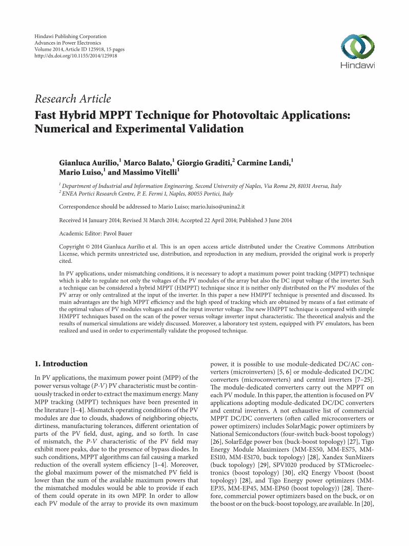
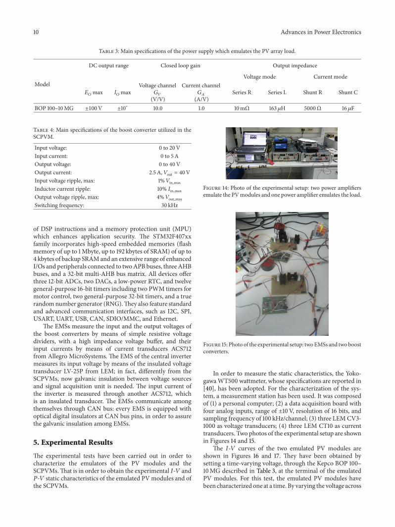
In order to measure the static characteristics, the Yoko-gawaWT500 wattmeter, whose specifications are reported in[40], has been adopted. For the characterization of the sys-tem, a measurement station has been used. It was composedof (1) a personal computer; (2) a data acquisition board withfour analog inputs, range of ±10V, resolution of 16 bits, andsampling frequency of 100 kHz/channel; (3) three LEMCV3-1000 as voltage transducers; (4) three LEM CT10 as currenttransducers. Two photos of the experimental setup are shownin Figures 14 and 15.
The 𝐼-𝑉 curves of the two emulated PV modules areshown in Figures 16 and 17. They have been obtained bysetting a time-varying voltage, through the Kepco BOP 100–10MG described in Table 3, at the terminal of the emulatedPV modules. For this test, the emulated PV modules havebeen characterized one at a time. By varying the voltage across

Advances in Power Electronics 11
0 2 4 6 8 10 12 14 160
2
4
6
Voltage (V)
Curr
ent (
A)
Experimental I-V characteristic-module 1
(a)
0 2 4 6 8 10 12 14 16
00.20.40.6
Voltage (V)
Dev
iatio
n (A
)
−0.2
Deviation among experimental and desired I-V characteristics
(b)
Figure 16: 𝐼-𝑉 characteristic of emulated PV module 1 and devia-tion with respect to the desired one.
0 5 10 150
2
4
6
Voltage (V)
Curr
ent (
A)
Experimental I-V characteristic-module 2
(a)
0 5 10 15
00.20.40.6
Voltage (V)
Dev
iatio
n (A
)
−0.2
Deviation among experimental and desired I-V characteristics
(b)
Figure 17: 𝐼-𝑉 characteristic of the emulated PV module 2 anddeviation with respect to the desired one.
the emulated PV modules terminals and by measuring thecorresponding currents, the 𝐼-𝑉 curves can be obtained. InFigures 16 and 17, the deviations with respect to the desiredcharacteristics of Figure 13 are shown.
The same test has been performed by connecting the twomodules in series.The 𝑃-𝑉 curve of the two series connectedmodules is shown in Figure 18. It can be seen that, since thetwomodules are exposed to different solar radiations, the𝑃-𝑉curve exhibits two maxima. The maximum power is reachedin correspondence with about 25V and it is equal to about65W. The relative maximum power point is located at about11 V, and its power is equal to about 52W.
Then, the emulated PV modules have been connectedto the corresponding boost DC/DC converters and EMSs,in order to obtain two SCPVMs. The two SCPVMs havebeen characterized in the same way of the two emulated PV
0 5 10 15 20 25 300
10
20
30
40
50
60
70
Voltage (V)
Pow
er (W
)
Experimental P-V characteristic of series connected PV modules
Figure 18: 𝑃-𝑉 characteristic of the two series connected emulatedPV modules.
0 5 10 15 20 25 305
10152025303540455055
SCPVM 1SCPVM 2
Voltage (V)
Pow
er (W
)
Experimental P-V characteristics
Figure 19: Output powers of the emulated PV modules versus theoutput voltage of the corresponding SCPVMs.
modules, as described at the beginning of this subsection,that is, by setting a time-varying voltage and by measuringthe corresponding current. In this test, they have not beenconnected in series and they have been characterized one ata time. Figure 19 shows the output powers of the emulatedPV modules versus the output voltage of the correspondingSCPVMs. As it can be seen, until the output voltage ofthe SCPVM does not reach the maximum power pointvoltage 𝑉MPP, the power increases with the voltage; in theseconditions, the EMS lets the boost converter work at zeroduty cycle; that is, the boost input and output voltagesvalues are the same. When the output voltage of the SCPVMreaches 𝑉MPP, the EMS forces the boost to increase its dutycycle, in order to maintain 𝑉MPP across the emulated PVmodule. Therefore, even in correspondence with SCPVMsoutput voltages values which are higher than𝑉MPP, the outputpowers of the emulated PV modules are constant and equalto their maximum possible value.
The same test has been performed by connecting the twoSCPVMs in series. Figure 20 shows the 𝑃-𝑉 characteristic ofthe two series connected SCPVMs. Comparing such a curvewith the 𝑃-𝑉 characteristic of Figure 18, some considerationscan be drawn. First of all, the PV maximum power extracted

12 Advances in Power Electronics
0 10 20 30 40 50 600
102030405060708090
100
Voltage (V)Po
wer
(W)
Experimental P-V characteristics
Figure 20: 𝑃-𝑉 characteristic of the string of the two SCPVMs.
2 2.5 3 3.5 4 4.5 505
1015
Time (s)
Time domain voltage and current-module 1
Volta
ge (V
)
(a)
2 2.5 3 3.5 4 4.5 54
4.5
5
Time (s)Cu
rren
t (A
)
(b)
Figure 21: Steady-state voltage and current of the emulated PV module 1 in the first test.
2 2.5 3 3.5 4 4.5 50246
Time (s)
Volta
ge (V
)
Time domain voltage and current-module 2
(a)
2 2.5 3 3.5 4 4.5 5
3
3.1
3.2
Curr
ent (
A)
Time (s)
(b)
Figure 22: Steady-state voltage and current of the emulated PVmodule 2 in the first test.
in the case of the string of SCPVMs (about 73W) is higherthan the corresponding power obtained in the case of thestring of PV modules (about 65W). Secondly, in the case ofthe string of SCPVMs, there are no local maxima in whichthe CMPPT inverter controller can force the system to work.Thirdly, in the case of the string of SCPVMs, the power isconstant and assumes its maximum value in a wide voltagerange (from about 27V to about 65V) rather than in a singleoperating point (i.e., 25V in Figure 18).
It is important to underline that such experimentalresults are in full agreement with the theoretical predictionsdiscussed in Section 2.
2 2.5 3 3.5 4 4.5 520
30
40
50
60
70
80
Time (s)
Pow
er (W
)
Figure 23: Steady-state total output power of the series connectedSCPVMs in the first test.
In order to obtain a further verification of the theoreticalpredictions, two additional tests have been performed. In thefirst test, the string of the two SCPVMs is forced to workwith a constant voltage equal to about 15V. Figure 21 showsthe steady-state voltage and the steady-state current of theemulated PV module 1, while Figure 22 shows the steady-state voltage and the steady-state current of the emulatedPV module 2. Figure 23 shows instead the total steady-stateoutput power of the two emulated PVmodules. In accordancewith the theoretical predictions, it can be seen that themodule exposed to the lower solar radiation provides nooutput power at the steady-state since it works in output shortcircuit conditions. Coherently with Figure 19, fromFigure 23,it can be seen that the total output power corresponds to theoutput power of the only PVmodule 1 and it is equal to about56W.

Advances in Power Electronics 13
2 2.5 3 3.5 4 4.5 5 5.505
1015
Time (s)
Time domain voltage and current-module 1Vo
ltage
(V)
(a)
2 2.5 3 3.5 4 4.5 5 5.54
4.5
5
Curr
ent (
A)
Time (s)
(b)
Figure 24: Steady-state voltage and current of the emulated PV module 1 in the second test.
2.5 3 3.5 4 4.5 505
1015
Time domain voltage and current-module 2
Time (s)
Volta
ge (V
)
(a)
2.5 3 3.5 4 4.5 52.6
2.8
3
Curr
ent (
A)
Time (s)
(b)
Figure 25: Steady-state voltage and current of the emulated PV module 2 in the second test.
2.5 3 3.5 4 4.5 520
40
60
80
100
120
Time (s)
Pow
er (W
)
Figure 26: Steady-state total output power of the series connectedSCPVMs in the second test.
In the second test, the string of SCPVMs is forced to workwith a constant voltage equal to about 45V. Figure 24 showsthe steady-state voltage and the steady-state current of theemulated PV module 1, while Figure 25 shows the steady-state voltage and the steady-state current of the emulated PVmodule 2. Figure 26 shows the total steady-state output powerof the series connected SCPVMs. In this case, in accordancewith the theoretical predictions, it can be seen that boththe two modules provide their maximum power. Coherentlywith Figure 19, from Figure 26, it can be seen that the totaloutput power corresponds to the sum of the output powersof module 1 and module 2 and it is equal to about 89W.
6. Conclusions
In PV applications, undermismatching conditions, the adop-tion of a MPPT technique which is able to regulate notonly the voltages of the PV modules of the array but alsothe DC input voltage of the inverter is necessary. Such atechnique can be considered a hybridMPPT techniquewhichis neither only distributed on the PV modules of the PV
array or only centralized at the input of the inverter. In thispaper, a new HMPPT technique is presented and discussed.Its main advantages are the high MPPT efficiency and thehigh speed of tracking obtained by means of a fast estimateof the optimal voltages of the PVmodules and of the inverter.The mathematical formulation of the technique has beendeeply discussed. Numerical simulations allowing comparingthe performances of the presented technique with those onesof another HMPPT technique have been also shown. Aprototype of the embedded measurement system which hasto be applied to each PV module in order to implement theDMPPT technique has been realized.Thedifferent embeddedmeasurement systems of the same PVplant can communicateamong themselves through optical-insulatedCANbus.A lab-oratory measurement setup has been realized and it has beenused to test the prototypes.The obtained experimental resultsare in very good agreement with the results of numericalsimulations and assess the validity of the method. In partic-ular, it has been demonstrated that, even under mismatchedconditions, the proposed system allows each PV module ofthe array to work in its MPP. That is, differently from thecase of the string of PV modules, in the case of the string ofSCPVMs, themaximum total PV output power is equal to thesum of the maximum powers of the single PV modules.
Conflict of Interests
The authors declare that there is no conflict of interestsregarding the publication of this paper.
References
[1] N. Femia, G. Petrone, G. Spagnuolo, and M. Vitelli, “Optimiza-tion of perturb and observe maximum Power Point Trackingmethod,” IEEE Transactions on Power Electronics, vol. 20, no. 4,pp. 963–973, 2005.

14 Advances in Power Electronics
[2] T. Esram andP. L. Chapman, “Comparison of photovoltaic arraymaximum Power Point Tracking techniques,” IEEE Transac-tions on Energy Conversion, vol. 22, no. 2, pp. 439–449, 2007.
[3] N. Femia, G. Petrone, G. Spagnuolo, and M. Vitelli, “A newanalog MPPT technique: TEODI,” Progress in Photovoltaics:Research and Applications, vol. 18, no. 1, pp. 28–41, 2010.
[4] D. P. Hohm and M. E. Ropp, “Comparative study of maximumPower Point Tracking algorithms,” Progress in Photovoltaics:Research and Applications, vol. 11, no. 1, pp. 47–62, 2003.
[5] S. B. Kjaer, J. K. Pedersen, and F. Blaabjerg, “A review of single-phase grid-connected inverters for photovoltaicmodules,” IEEETransactions on Industry Applications, vol. 41, no. 5, pp. 1292–1306, 2005.
[6] Q. Li and P. Wolfs, “A review of the single phase photovoltaicmodule integrated converter topologies with three different DClink configurations,” IEEE Transactions on Power Electronics,vol. 23, no. 3, pp. 1320–1333, 2008.
[7] R. Alonso, P. Ibanez, V.Martınez, E. Roman, andA. Sanz, “Anal-ysis of performance of new distributed MPPT architectures,” inProceedings of the IEEE International Symposium on IndustrialElectronics (ISIE ’10), pp. 3450–3455, July 2010.
[8] M. Balato, M. Vitelli, N. Femia, G. Petrone, and G. Spagnuolo,“Factors limiting the efficiency of DMPPT in PV applications,”in Proceedings of the 3rd International Conference on CleanElectrical Power: Renewable Energy Resources Impact (ICCEP’11), pp. 604–608, Ischia, Italy, June 2011.
[9] J. Huusari and T. Suntio, “Origin of cross-coupling effects indistributed DC-DC converters in photovoltaic applications,”IEEETransactions on Power Electronics, vol. 28, no. 10, pp. 4625–4635, 2013.
[10] G. Petrone, C. A. Ramos-Paja, G. Spagnuolo, and M. Vitelli,“Granular control of photovoltaic arrays by means of a multi-output maximum Power Point Tracking algorithm,” Progress inPhotovoltaics: Research and Applications, vol. 21, no. 5, pp. 918–932, 2013.
[11] S. M. MacAlpine, R. W. Erickson, and M. J. Brandemuehl,“Characterization of power optimizer potential to increaseenergy capture in photovoltaic systems operating undernonuniform conditions,” IEEE Transactions on Power Electron-ics, vol. 28, no. 6, pp. 2936–2945, 2013.
[12] S. Vighetti, J.-P. Ferrieux, and Y. Lembeye, “Optimizationand design of a cascaded DC/DC converter devoted to grid-connected photovoltaic systems,” IEEE Transactions on PowerElectronics, vol. 27, no. 4, pp. 2018–2027, 2012.
[13] S. Poshtkouhi, V. Palaniappan, M. Fard, and O. Trescases, “Ageneral approach for quantifying the benefit of distributedpower electronics for fine grained MPPT in photovoltaicapplications using 3D modeling,” IEEE Transactions on PowerElectronics, vol. 99, no. 11, pp. 4656–4666, 2011.
[14] M. S. Agamy, S. Chi, A. Elasser et al., “A high-power-densityDC-DC converter for distributed PV architectures,” IEEE Jour-nal of Photovoltaics, vol. 3, no. 2, pp. 791–798, 2013.
[15] D. Shmilovitz and Y. Levron, “Distributed maximum PowerPoint Tracking in photovoltaic systems—emerging architec-tures and control methods,” Automatika: Journal for Control,Measurement, Electronics, Computing andCommunications, vol.53, no. 2, 2012.
[16] A. I. Bratcu, I. Munteanu, S. Bacha, D. Picault, and B. Raison,“Cascaded DCDC converter photovoltaic systems: power opti-mization issues,” IEEE Transactions on Industrial Electronics,vol. 58, no. 2, pp. 403–411, 2011.
[17] C. Olalla, C. Deline, and D. Maksimovic, “Performance of mis-matched PV systems with submodule integrated converters,”IEEE Journal of Photovoltaics, vol. 4, no. 1, pp. 396–404, 2014.
[18] C. Olalla, M. Rodriguez, D. Clement, and D. Maksimovic,“Architectures and control of submodule integrated DC-DCconverters for photovoltaic applications,” IEEE Transactions onPower Electronics, vol. 28, no. 6, pp. 2980–2997, 2013.
[19] R. C. N. Pilawa-Podgurski and D. J. Perreault, “Submoduleintegrated distributed maximum Power Point Tracking forsolar photovoltaic applications,” IEEE Transactions on PowerElectronics, vol. 28, no. 6, pp. 2957–2967, 2013.
[20] G. R. Walker and P. C. Sernia, “Cascaded DC-DC converterconnection of photovoltaic modules,” IEEE Transactions onPower Electronics, vol. 19, no. 4, pp. 1130–1139, 2004.
[21] N. Femia, G. Lisi, G. Petrone, G. Spagnuolo, and M. Vitelli,“Distributed maximum Power Point Tracking of photovoltaicarrays: novel approach and system analysis,” IEEE Transactionson Industrial Electronics, vol. 55, no. 7, pp. 2610–2621, 2008.
[22] C. Deline, B. Marion, J. Granata, and S. Gonzalez, “A perfor-mance and economic analysis of distributed power electronicsin photovoltaic systems,” Technical Report NREL/TP-5200-50003, 2011.
[23] G. Graditi, G. Adinolfi, andG.M. Tina, “Photovoltaic optimizerboost converters: temperature influence and electro-thermaldesign,” Applied Energy, vol. 115, pp. 140–150, 2014.
[24] G. Graditi, G. Adinolfi, N. Femia, and M. Vitelli, “Comparativeanalysis of synchronous rectification boost and diode rectifica-tion boost converter for DMPPT applications,” in Proceedingsof the IEEE International Symposium on Industrial Electronics(ISIE ’11), pp. 1000–1005, Gdansk, Poland, June 2011.
[25] G. Graditi and G. Adinolfi, “Energy performances and reli-ability evaluation of an optimized DMPPT boost converter,”in Proceedings of the 3rd International Conference on CleanElectrical Power: Renewable Energy Resources Impact (ICCEP’11), pp. 69–72, Ischia, Italy, June 2011.
[26] http://solarmagic.com/en/index.html.[27] http://www.solaredge.com.[28] http://www.tigoenergy.com.[29] http://www.xandex.com.[30] http://www.st.com.[31] M. Vitelli, “On the necessity of joint adoption of both dis-
tributedmaximumPower Point Tracking and centralmaximumPower Point Tracking in PV systems,” Progress in Photovoltaics:Research and Applications, vol. 22, no. 3, pp. 283–299, 2014.
[32] N. Femia, G. Petrone, G. Spagnuolo, and M. Vitelli, Power Elec-tronics and Control Techniques ForMaximumEnergy Harvestingin Photovoltaic Systems, CRC Press, Taylor & Francis Group,New York, NY, USA, 2013.
[33] M. Balato, D. Gallo, C. Landi, M. Luiso, and M. Vitelli, “Designand implementation of a hybrid MPPT technique based onthe scan of the power versus voltage input characteristic ofthe inverter,” in Proceedings of 19th IMEKO TC 4 Symposiumand 17th IWADC Workshop, Advances in Instrumentation andSensors Interoperability, Barcelona, Spain, July 2013.
[34] M. Balato and M. Vitelli, “A new strategy for the identificationof optimal operating points in PV applications with DistributedMPPT,” in Proceedings of the 8th International Conference andEcological Vehicles and Renewable Energies (EVER ’13), pp. 1–7,Monte Carlo, Monaco, March 2013.

Advances in Power Electronics 15
[35] M. Balato and M. Vitelli, “A hybrid MPPT technique basedon the fast estimate of the maximum power voltages in PVapplications,” in Proceedings of the 8th International Conferenceand Ecological Vehicles and Renewable Energies (EVER ’13), pp.1–6, Monte Carlo, Monaco, March 2013.
[36] S. Liu and R. A. Dougal, “Dynamicmultiphysicsmodel for solararray,” IEEETransactions on Energy Conversion, vol. 17, no. 2, pp.285–294, 2002.
[37] D. T. Lobera and S. Valkealahti, “Dynamic thermal model ofsolar PV systems under varying climatic conditions,” SolarEnergy, vol. 93, pp. 183–194, 2013.
[38] R.W. Erikson and D.Maksimovic, Fundamentals of Power Elec-tronics, Kluwer Academic, Norwell, Mass, USA, 2nd edition,2001.
[39] M. Balato, D. Gallo, C. Landi, M. Luiso, and M. Vitelli,“Simulation and laboratory characterization of a hybrid MPPTtechnique based on the fast estimate of the maximum powervoltages in PV applications,” in Proceedings of IEEE Interna-tional Instrumentation andMeasurement Technology Conference(I2MTC ’13), Minneapolis, MN, USA, May 2013.
[40] http://tmi.yokogawa.com/products/digital-power-analyzers/digital-power-analyzers/wt500-power-analyzer/.

International Journal of
AerospaceEngineeringHindawi Publishing Corporationhttp://www.hindawi.com Volume 2014
RoboticsJournal of
Hindawi Publishing Corporationhttp://www.hindawi.com Volume 2014
Hindawi Publishing Corporationhttp://www.hindawi.com Volume 2014
Active and Passive Electronic Components
Control Scienceand Engineering
Journal of
Hindawi Publishing Corporationhttp://www.hindawi.com Volume 2014
International Journal of
RotatingMachinery
Hindawi Publishing Corporationhttp://www.hindawi.com Volume 2014
Hindawi Publishing Corporation http://www.hindawi.com
Journal ofEngineeringVolume 2014
Submit your manuscripts athttp://www.hindawi.com
VLSI Design
Hindawi Publishing Corporationhttp://www.hindawi.com Volume 2014
Hindawi Publishing Corporationhttp://www.hindawi.com Volume 2014
Shock and Vibration
Hindawi Publishing Corporationhttp://www.hindawi.com Volume 2014
Civil EngineeringAdvances in
Acoustics and VibrationAdvances in
Hindawi Publishing Corporationhttp://www.hindawi.com Volume 2014
Hindawi Publishing Corporationhttp://www.hindawi.com Volume 2014
Electrical and Computer Engineering
Journal of
Advances inOptoElectronics
Hindawi Publishing Corporation http://www.hindawi.com
Volume 2014
The Scientific World JournalHindawi Publishing Corporation http://www.hindawi.com Volume 2014
SensorsJournal of
Hindawi Publishing Corporationhttp://www.hindawi.com Volume 2014
Modelling & Simulation in EngineeringHindawi Publishing Corporation http://www.hindawi.com Volume 2014
Hindawi Publishing Corporationhttp://www.hindawi.com Volume 2014
Chemical EngineeringInternational Journal of Antennas and
Propagation
International Journal of
Hindawi Publishing Corporationhttp://www.hindawi.com Volume 2014
Hindawi Publishing Corporationhttp://www.hindawi.com Volume 2014
Navigation and Observation
International Journal of
Hindawi Publishing Corporationhttp://www.hindawi.com Volume 2014
DistributedSensor Networks
International Journal of