o.h.w. siegmund, - kiss.caltech.edu
TRANSCRIPT

O.H.W. Siegmund, aExperimental Astrophysics Group, Space Sciences Laboratory, 7 Gauss Way, University of
California, Berkeley, CA 94720

MicrochannelMicrochannel Plate Development EffortsPlate Development Efforts
Microchannel Plates – large (& small) area advanced technologyDevelopment study to produce small pore, large area MCPs with borosilicate glass substrates and atomic layer deposited resistive layer and secondary electron emissive , with high quality imaging, high spatial resolution, low background and high QDE (compatibility with high
h h d d i i )
PhotocathodesLots of efforts in GaN opaque and semitransparent photocathodes
temperature photocathode depositions).
p q p pThere are also other developments at different wavelength regimes
Readout and ElectronicsCurrent readout work is focused on cross strip charge division anodesAnd high speed position and time encoding electronics.
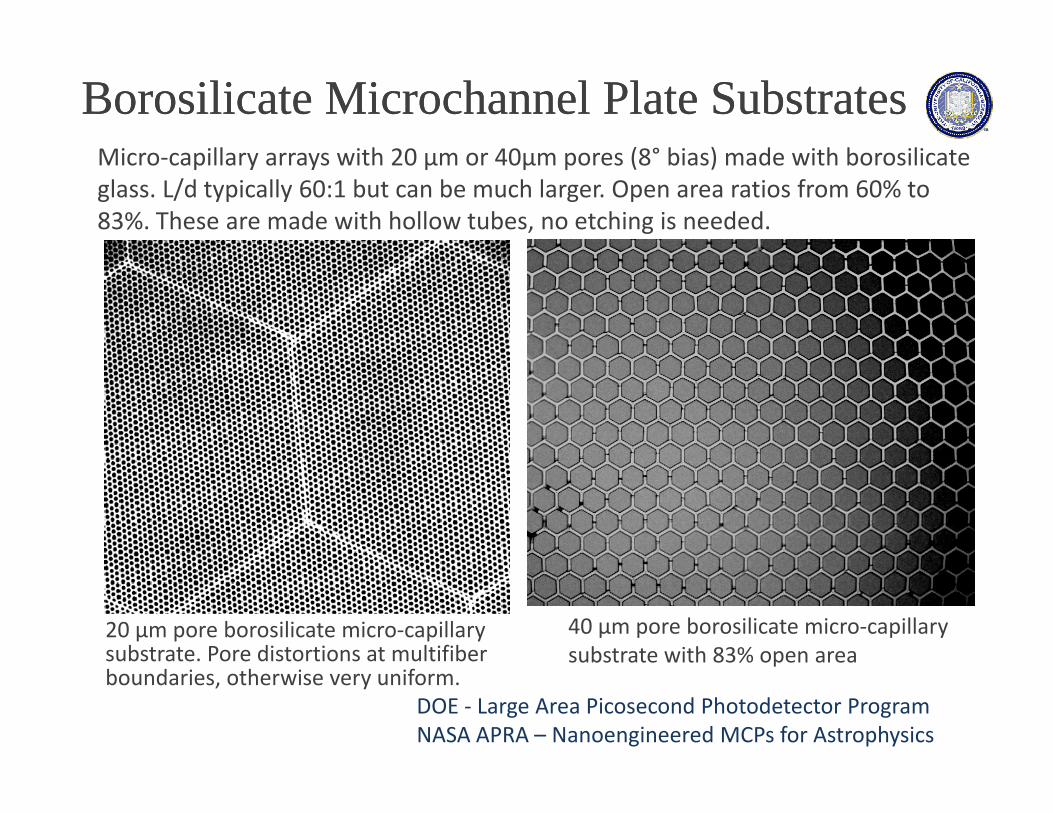
Mi ill ith 20 40 (8° bi ) d ith b ili t
Borosilicate Borosilicate MicrochannelMicrochannel Plate Substrates Plate Substrates Micro‐capillary arrays with 20 µm or 40µm pores (8° bias) made with borosilicate glass. L/d typically 60:1 but can be much larger. Open area ratios from 60% to 83%. These are made with hollow tubes, no etching is needed.
20 µm pore borosilicate micro‐capillary substrate. Pore distortions at multifiber
40 µm pore borosilicate micro‐capillary substrate with 83% open area
boundaries, otherwise very uniform.p
DOE ‐ Large Area Picosecond Photodetector ProgramNASA APRA – Nanoengineered MCPs for Astrophysics

Borosilicate Substrate Atomic Layer Borosilicate Substrate Atomic Layer Deposited Deposited MicrochannelMicrochannel PlatesPlatespp
Micro‐capillary arrays with 20 µm or 40µm pores (8° bias) made with borosilicate glass. Resistive and secondary emissive layers are applied (Argonne Lab, Arradiance) to allowthese to function as MCP electron multipliers. Each step is separately engineered/optimized.
Visible light transmission for a 20 µm poreVisible light transmission for a 20 µm poreborosilicate micro‐capillary ALD MCP .
Surface photo for a 20 µm pore borosilicate micro‐capillary ALD MCP with NiCr electrode .

Single MCP Single MCP –– Phosphor Screen TestsPhosphor Screen Tests33mm 20µm pore borosilicate MCP substrate 60:1 L/d 8 degree pore bias 1100v MCP33mm, 20µm pore borosilicate MCP substrate, 60:1 L/d, 8 degree pore bias. 1100v MCP.
100 E3MCP Gain, input 20 pA e‐
1,000
10 E3
MCP 145
MCP 146
10
100
Gain
0.1
1
400 600 800 1000 1200 1400
Single MCP tests in DC amplification mode show imaging and gain very similar to
400 600 800 1000 1200 1400
MCP HV (volts)
g p g g g yconventional MCPs. Sample imaging performance has improved dramatically over the last 12 months due to process improvements.
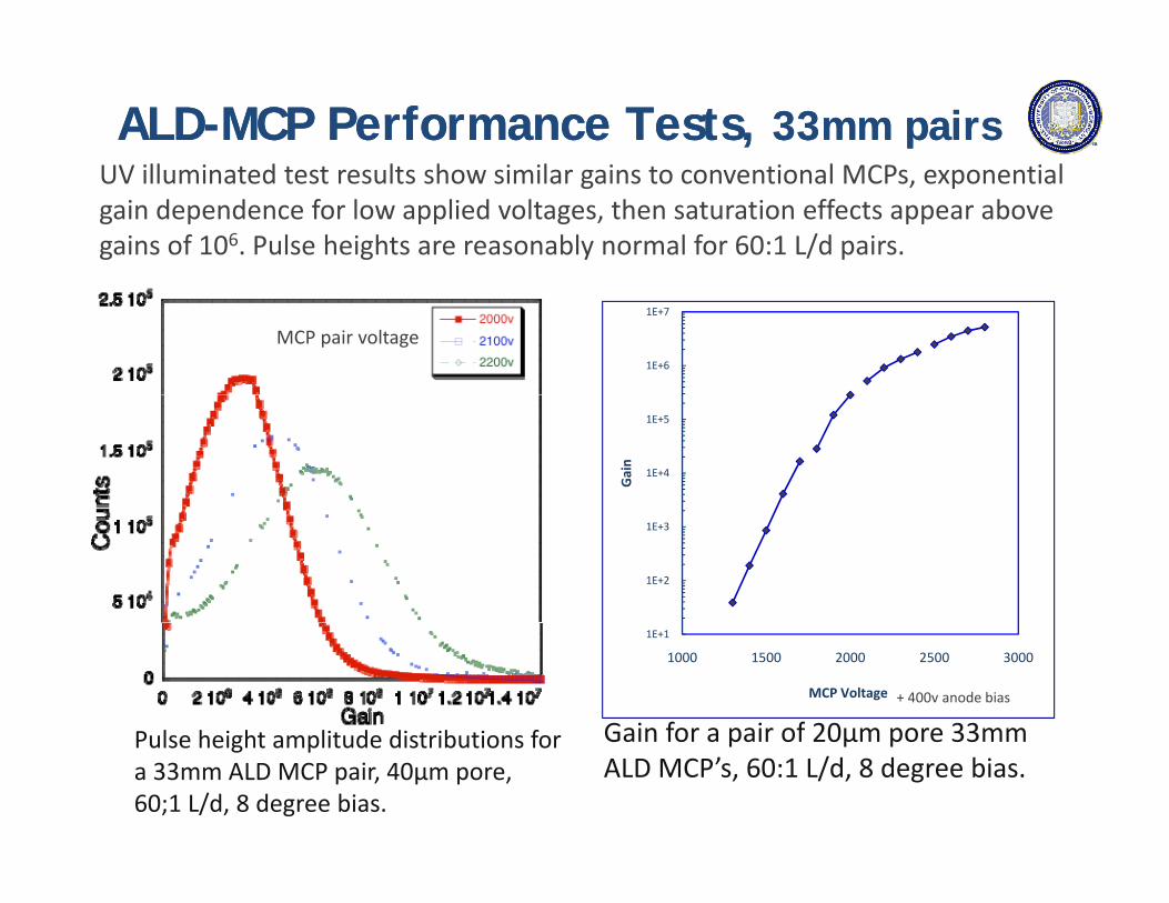
ALDALD--MCP Performance Tests, MCP Performance Tests, 33mm pairs 33mm pairs UV ill i t d t t lt h i il i t ti l MCP ti lUV illuminated test results show similar gains to conventional MCPs, exponential gain dependence for low applied voltages, then saturation effects appear above gains of 106. Pulse heights are reasonably normal for 60:1 L/d pairs.
1E+6
1E+7
MCP pair voltage
1E+4
1E+5
Gain
1E+2
1E+3
1E+1
1000 1500 2000 2500 3000
MCP Voltage
Gain for a pair of 20µm pore 33mmPulse height amplitude distributions for
+ 400v anode bias
Gain for a pair of 20µm pore 33mm ALD MCP’s, 60:1 L/d, 8 degree bias.
Pulse height amplitude distributions for a 33mm ALD MCP pair, 40µm pore, 60;1 L/d, 8 degree bias.

Photon Counting Imaging with MCP PairsPhoton Counting Imaging with MCP PairsMCP i 20 8° bi 60 1 L/d 0 7 i ith 300V biMCP pair, 20µm pores, 8° bias, 60:1 L/d, 0.7mm pair gap with 300V bias.
Image of 185nm UV light, shows top MCP hexmodulation (sharp) and faint MCP hexagonal
Gain map (average gain), shows top MCP hex modulation (sharp) and a fewmodulation (sharp) and faint MCP hexagonal
modulation from bottom MCP. A few defects, but generally very good. Edge effects are field fringing due to the MCP support flange.
MCP hex modulation (sharp) and a few spots where the gain is low.

ALDALD--MCP Background RateMCP Background RateMCP i 20 8° bi 60 1 L/d 0 7 i ith 300V biMCP pair, 20µm pores, 8° bias, 60:1 L/d, 0.7mm pair gap with 300V bias.
Pulse amplitude distributions for UV185nm and for background events
3000 sec background, 0.0845 events cm‐2 sec‐1. at 7 x 10⁶ gain, 1050v bias on each MCP. Get
b h f ll f h 185nm, and for background events.same behavior for all of the current 20µm MCPs
MCPs rad hard, low radioactivity, low cross section (no lead)

33mm ALD33mm ALD--MCP Preconditioning TestsMCP Preconditioning Tests
Scrubbing with UV after 350°C bake Ageing test after 150°C bake
10000
100
1000
10000
t (nA
)
QExt = 0.00 C/cm2
QExt = 0.32 C/cm2
QExt = 1.30 C/cm2
QExt = 1.72 C/cm2
10
100
ted Ph
otocurrent QExt = 2.11 C/cm2
QExt = 2.54 C/cm2
QExt = 2.73 C/cm2
QExt = 3.11 C/cm2
0.1
1
Correct
Scrub of ALD MCP pair (20µm pore,
0.01
0 500 1000 1500
MCP HV (volts)
60:1 L/d, 8° bias) compared with conventional MCPs. UV input.
Scrub of single ALD MCP (20µm pore, 60:1 L/d, 8° bias) after 150 °C bakeout.

ALDALD--MCP Quantum EfficiencyMCP Quantum EfficiencyALD borosilicate MCP photon counting ALD secondary emissive layer on normalALD – borosilicate MCP photon counting quantum detection efficiency, normal NiCrelectrode coating gives normal bare MCP QE.
ALD – secondary emissive layer on normalMCP gives good “bare” QDE. CsI depositedon this gives a good “standard” CsI QDE.
QDE for bare MCP with ALD secondary #375 & #613 MCP pairs, 20µm pores, 8° bias,
10
yemissive layer, and with CsI deposited on top of this.
#375 & #613 MCP pairs, 20µm pores, 8 bias, 60:1 L/d, 60% OAR. #31 MCP pair, 40µm pores8° bias, 60:1 L/d, 83% OAR, shows higher QDE.
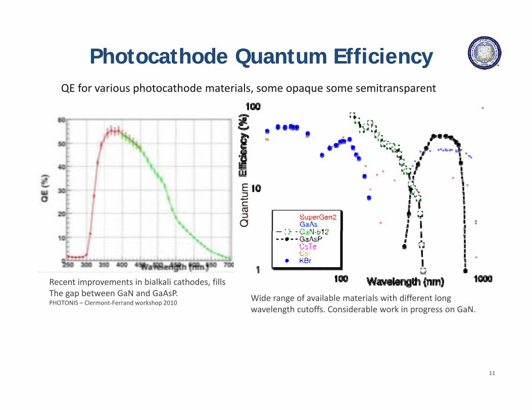
Photocathode Quantum EfficiencyPhotocathode Quantum EfficiencyQE for various photocathode materials, some opaque some semitransparent
Recent improvements in bialkali cathodes fillsRecent improvements in bialkali cathodes, fillsThe gap between GaN and GaAsP.PHOTONIS – Clermont‐Ferrand workshop 2010
Wide range of available materials with different long wavelength cutoffs. Considerable work in progress on GaN.
11

Opaque Opaque GaNGaN Deposited on SapphireDeposited on Sapphire
GaN semitransparent and opaque photocathode quantum efficiencies. The GaN is 150nm to 100nm thick with depth graded Mg concentration The best semitransparent QE is for a
12
to 100nm thick with depth graded Mg concentration. The best semitransparent QE is for a substrate with only 50% GaN coverage ‐ hence the achievable efficiency is probably closer to twice the measured values.

ili / C d b i h d d G / l f i hi k
Opaque Opaque GaNGaN Deposited on ALD Deposited on ALD MCPsMCPsBorosilicate/ALD MCP coated by MBE with P‐doped GaN/AlN of various thicknesses(amorphous/polycrystalline) and tested in a photon counting imaging detector
Integrated photon counting image using 184 nm UV shows unprocessed
Photo of 20µm pore MCP with zonesof different GaN thickness and structureusing 184 nm UV shows unprocessed
GaN layer response vs bare MCP.of different GaN thickness and structure,Deposited by SVT associates (A. Dabiran).
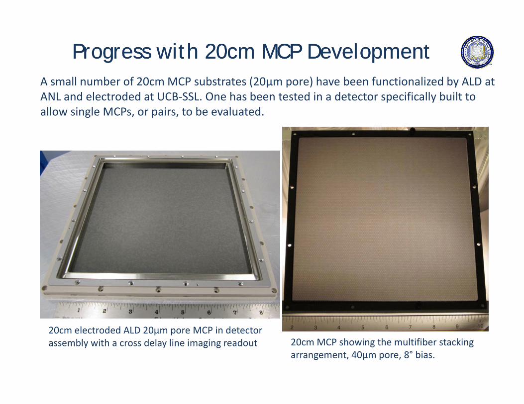
Progress Progress withwith 20cm MCP Development20cm MCP DevelopmentA small number of 20cm MCP substrates (20µm pore) have been functionalized by ALD at ANL and electroded at UCB‐SSL. One has been tested in a detector specifically built to allow single MCPs, or pairs, to be evaluated.
20cm electroded ALD 20µm pore MCP in detector20cm electroded ALD 20µm pore MCP in detector assembly with a cross delay line imaging readout 20cm MCP showing the multifiber stacking
arrangement, 40µm pore, 8° bias.

Testing of 20cm, 20µm pore ALDTesting of 20cm, 20µm pore ALD--MCPsMCPs
An initial test with one 20cm, 20µm pore, 60:1 L/d ALD‐MCP shows a normal MCP gain curve The cross delay line detector accepts 2 MCPs and spacers It will allow <200µm
20cm MCP strip current and resistance 20cm MCP output signal v.s. V for UV input
curve.The cross delay line detector accepts 2 MCPs and spacers. It will allow <200µm spatial resolution for MCP pairs, and permit full evaluation of 20cm MCPs.
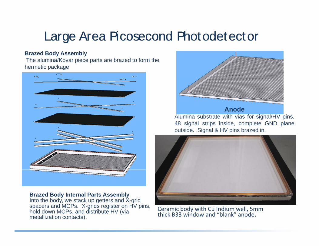
Large Area Large Area PicosecondPicosecond PhotodetectorPhotodetectorBrazed Body AssemblyThe alumina/Kovar piece parts are brazed to form the hermetic package
A dAnodeAlumina substrate with vias for signal/HV pins.48 signal strips inside, complete GND planeoutside. Signal & HV pins brazed in.
Brazed Body Internal Parts AssemblyInto the body we stack up getters and X-gridInto the body, we stack up getters and X-gridspacers and MCPs. X-grids register on HV pins,hold down MCPs, and distribute HV (via metallization contacts).
Ceramic body with Cu Indium well, 5mm thick B33 window and “blank” anode.

Cross Strip Anode MCP DetectorsCross Strip Anode MCP DetectorsCh di id b t th t t i t t i t t id i X d YCharge divides between the two strip sets to give event centroids in X and YUses lower gain (~5 x 10⁵), works open face or in sealed tube configurations< 15 µm FWHM spatial resolution, current formats from 22mm to 50mm, and 100mmCurrent SMT electronics allows ~5 MHz event rates, ASIC electronics under development
Ph t th d t
p
• Photocathode converts photon to electron
• MCP(s) amplify electron by 104 to 105
• Rear field accelerates electrons to anode
• Strip anode encodes charge cloudcharge cloud
17
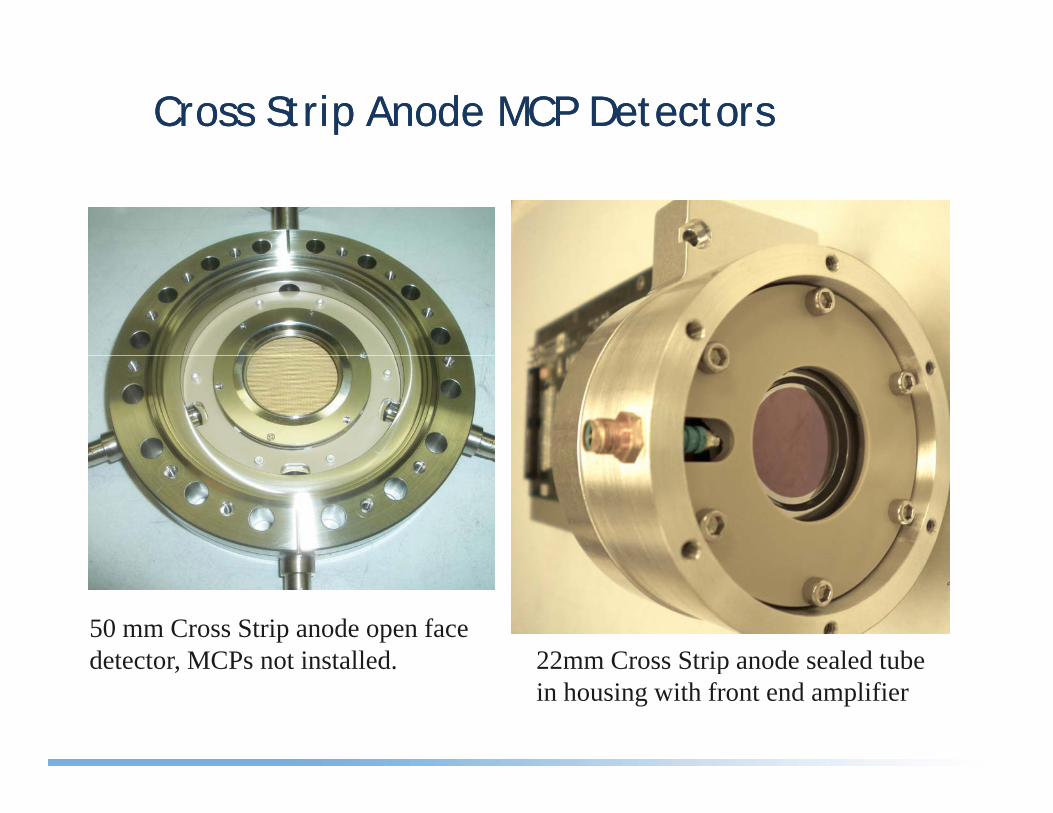
Cross Strip Anode MCP DetectorsCross Strip Anode MCP Detectors
50 mm Cross Strip anode open facedetector MCPs not installed 22mm Cross Strip anode sealed tubedetector, MCPs not installed. 22mm Cross Strip anode sealed tube
in housing with front end amplifier