novel technologies for elastic microsystems: development
TRANSCRIPT

“FB˙doctoraat2” — 2011/1/27 — 10:56 — page 1 — #1�
�
�
�
�
�
�
�
Nieuwe technologieen voor elastische microsystemen:
ontwikkeling, karakterisering en toepassingen.
Novel Technologies for Elastic Microsystems:
Development, Characterization and Applications.
Frederick Bossuyt
Promotor: Prof. dr. ir. J. Vanfleteren
Proefschrift ingediend tot het behalen van de graad vanDoctor in de IngenieurswetenschappenElektrotechniek
Vakgroep Elektronica en InformatiesystemenVoorzitter: Prof. dr. ir. J. Van CampenhoutFaculteit IngenieurswetenschappenAcademiejaar 2010–2011

“FB˙doctoraat2” — 2011/1/27 — 10:56 — page 2 — #2�
�
�
�
�
�
�
�

“FB˙doctoraat2” — 2011/1/27 — 10:56 — page 3 — #3�
�
�
�
�
�
�
�
Nieuwe technologieen voor elastische microsystemen:
ontwikkeling, karakterisering en toepassingen.
Novel Technologies for Elastic Microsystems:
Development, Characterization and Applications.
Frederick Bossuyt
Promotor: Prof. dr. ir. J. Vanfleteren
Proefschrift ingediend tot het behalen van de graad vanDoctor in de IngenieurswetenschappenElektrotechniek
Vakgroep Elektronica en InformatiesystemenVoorzitter: Prof. dr. ir. J. Van CampenhoutFaculteit IngenieurswetenschappenAcademiejaar 2010–2011

“FB˙doctoraat2” — 2011/1/27 — 10:56 — page 4 — #4�
�
�
�
�
�
�
�
ISBN 978-90-8578-400-5
NUR 959
Wettelijk depot: D/2011/10.500/5

“FB˙doctoraat2” — 2011/1/27 — 10:56 — page 5 — #5�
�
�
�
�
�
�
�
Promotor:
Prof. dr. ir. J. Vanfleteren
Onderzoeksgroep CMST MicrosystemsVakgroep Elektronica en InformatiesystemenTechnologiepark 914AB-9052 Zwijnaarde

“FB˙doctoraat2” — 2011/1/27 — 10:56 — page 6 — #6�
�
�
�
�
�
�
�

“FB˙doctoraat2” — 2011/1/27 — 10:56 — page i — #7�
�
�
�
�
�
�
�
Dankwoord
Eindelijk. Het ligt er. Natuurlijk raakt het me.Vier jaar lang zaten er puzzelstukken over ’Hoe elektronica uitrekbaar maken?’in m’n hoofd. Vier jaar lang probeerde ik met deze puzzelstukken een geheel tevormen. Een deel van de puzzel ligt hier voor je, een deel zal door enthousiastemensen verder vervolledigd worden.
Vele mensen droegen, bewust of onbewust, een puzzelstukje aan deze grote puzzelbij...
Eerst en vooral wil ik mijn promotor Jan Vanfleteren bedanken. Voor de kans diehij me gegeven heeft om aan dit onderzoek te kunnen werken. Verder bedankik hem ook voor de vrijheid die hij me in dit hele ontwikkelingsproces gaf, eenvrijheid die ik enorm apprecieerde. Bedankt voor het vertrouwen!Ook aan Andre Van Calster, leider van de CMST onderzoeksgroep, wil ik mijndank betuigen. Eerst en vooral voor het ter beschikking stellen van de infra-structuur, de omkadering,.. Bedankt ook voor de leuke barbecues, de gezelligeetentjes,..Verder bedank ik het ganse CMST team om op de een of andere manier, recht-streeks of onrechtstreeks bij te hebben gedragen aan wat ik de laatste 4 jaar ver-wezenlijkt heb. De lijst van mensen is lang, heel lang. Iedereen persoonlijk be-danken zou ons te ver leiden maar ik wil bij deze benadrukken: zonder jullie in-tellectuele, instrumentele, administratieve, motiverende steun was dit zeker nietgelukt. Bedankt!Een speciale dank gaat uit naar Wim, voor het (tot 2 maal toe) nauwgezet nalezenvan mijn proefschrift. De feedback heeft me enorm geholpen en vooral een gerustgevoel gegeven. Een dikke merci Wim, je hebt er nog (meer dan) ene te goed!Ook wil ik mijn bureaugenoten persoonlijk bedanken, voor het geven van kleuraan de dagelijkse sleur van het doctoraatsbestaan. Bjorn, Lieven, Fabrice, Pietro,Tomas, bedankt om allen op jullie (eigenzinnige) wijze te hebben bijgedragen aandit werk. Ook de vrouwelijke collega’s die een tijdje geleden nog op onze burovertoefden: Eva en Pritesh, het waren heel leuke momenten samen!

“FB˙doctoraat2” — 2011/1/27 — 10:56 — page ii — #8�
�
�
�
�
�
�
�
ii Dankwoord
Buiten CMST zijn er nog mensen die op professioneel vlak bijgedragen hebbenen een oprecht woord van dank verdienen:De mensen binnen Stella waarmee ik samengewerkt heb. In het bijzonder de col-lega’s (vrienden) van TU Berlijn - Thomas en Manuel. Ook Hans de Vries, voorde hele goeie samenwerking op het vlak van betrouwbaarheidstesten. Verderwil ik Mario Gonzalez en Hsu Yung-Yu bedanken voor het mechanische model-leer werk die ze verricht hebben, wat een zeer grote bijdrage betekent voor de(verdere) ontwikkeling van de voorgestelde technologieen.
Daarnaast zijn er nog een aantal mensen buiten het werk die natuurlijk een be-langrijke bijdrage hebben geleverd tot wat ik verwezenlijkt heb en heb kunnenverwezenlijken, zowel voor als tijdens mijn doctoraat.Mijn ouders, bedankt voor alle kansen die jullie me al gegeven hebben. Ik benjullie heel erg dankbaar. Ook mijn zus Laurence en Jonas, voor de goede banddie we al jaren hebben. En dan nog mijn rots in de branding, mijn allerliefsteAdinda. Merci voor alle steun en gewoon, omdat je er altijd bent voor mij.Ook mijn vrienden, in het bijzonder Thomas en Silvie en mijn nauw aan het hartliggende vrouwelijke kotgenoten, verdienen ook nog een plaatsje in deze ere gal-lerij.
Soms vragen mensen: was je niet beter meteen gaan ’werken’ in plaats van tedoctoreren? Wel, ik wil eindigen met te vertellen wat ik, naast de intellectuelevoldoening natuurlijk, aan het doctoreren te danken heb en wat me het meest isbijgebleven van de afgelopen 4 jaren...De conferenties naar San Francisco. Ik ben nog steeds verliefd op deze stad.De reis naar India was onvergetelijk... Dankzij Pritesh dit avontuur beleefd samenmet enkele collega’s en hun vriendin. Niet voor de hand liggend maar de helereis was onvergetelijk!Het CMST minivoetbal team. De kans gehad om een jaartje voorzitter te mogenzijn. Het enthousiasme van iedereen om mee te doen is onbeschrijflijk. Zelfs algaan we regelmatig op onze bek.De citytrip naar Barcelona, een weekend vol cava en tapas... en een beetje sportnatuurlijk, maar niet door mij.De gezellige barbecues die tot in de vroege uurtjes duurden, Duvelmomentjesincluis.Alle andere conferenties in binnen en buitenland: het eens gaan uitleggen vooreen internationaal gezelschap geeft wel een kick. En door te doctoreren wordt dewereld toch plots een stukje kleiner.De goeie buitenlandse contacten, vooral met de Duitsers. Ze hebben misschienwel een betere infrastructuur, wij hebben Gent met al zijn leuke plekjes, cafeswaar tot in de vroege uren gefeest kan worden. Ze zijn er meermaals onder deindruk van geweest.Nee, ik heb er zeker geen spijt van!

“FB˙doctoraat2” — 2011/1/27 — 10:56 — page iii — #9�
�
�
�
�
�
�
�
Contents
1 Introduction and research context 11.1 Elastic microsystems: approaches . . . . . . . . . . . . . . . . . . . . 1
1.1.1 Out-of-plane designs . . . . . . . . . . . . . . . . . . . . . . . 21.1.2 In-plane designs . . . . . . . . . . . . . . . . . . . . . . . . . 81.1.3 Combination of out-of-plane and in-plane designs . . . . . . 12
1.2 Elastic (opto)electronic devices . . . . . . . . . . . . . . . . . . . . . 131.2.1 Elastic (opto)electronic components . . . . . . . . . . . . . . 131.2.2 Elastic interconnects between rigid components . . . . . . . 151.2.3 Elastic integrated systems . . . . . . . . . . . . . . . . . . . . 231.2.4 Elastic power supplies . . . . . . . . . . . . . . . . . . . . . . 24
1.3 Scope of this PhD work . . . . . . . . . . . . . . . . . . . . . . . . . . 271.4 Research context . . . . . . . . . . . . . . . . . . . . . . . . . . . . . . 291.5 Research dissemination . . . . . . . . . . . . . . . . . . . . . . . . . . 32
2 Introduction to concepts related to elastic microsystems 402.1 System architecture and methodology . . . . . . . . . . . . . . . . . 402.2 Polymers . . . . . . . . . . . . . . . . . . . . . . . . . . . . . . . . . . 41
2.2.1 Classification by chain structure . . . . . . . . . . . . . . . . 422.2.2 Classification by polymerization structure . . . . . . . . . . 432.2.3 Classification by thermal behaviour . . . . . . . . . . . . . . 432.2.4 Embedding material: silicone . . . . . . . . . . . . . . . . . . 442.2.5 Supporting material: polyimide . . . . . . . . . . . . . . . . 48
2.3 Mechanical aspects of elastic microsystems . . . . . . . . . . . . . . 502.3.1 Mechanical characterization of embedding materials . . . . 502.3.2 Mechanical design of stretchable metallic interconnects . . . 53
2.4 Conclusions . . . . . . . . . . . . . . . . . . . . . . . . . . . . . . . . 64
3 Stretchable substrate technology 683.1 Introduction . . . . . . . . . . . . . . . . . . . . . . . . . . . . . . . . 683.2 General description of process flow . . . . . . . . . . . . . . . . . . . 683.3 Application of polymer on copper substrate . . . . . . . . . . . . . . 71

“FB˙doctoraat2” — 2011/1/27 — 10:56 — page iv — #10�
�
�
�
�
�
�
�
iv CONTENTS
3.4 Patterning of copper . . . . . . . . . . . . . . . . . . . . . . . . . . . 733.5 Application of soldermask . . . . . . . . . . . . . . . . . . . . . . . . 743.6 Copper surface finish . . . . . . . . . . . . . . . . . . . . . . . . . . . 753.7 Assembly of components . . . . . . . . . . . . . . . . . . . . . . . . . 763.8 Embedding . . . . . . . . . . . . . . . . . . . . . . . . . . . . . . . . . 773.9 Conclusions . . . . . . . . . . . . . . . . . . . . . . . . . . . . . . . . 78
4 Peelable technology 824.1 Introduction . . . . . . . . . . . . . . . . . . . . . . . . . . . . . . . . 824.2 General description of process flow . . . . . . . . . . . . . . . . . . . 834.3 Lamination of copper on carrier with temporary adhesive . . . . . 86
4.3.1 Copper type . . . . . . . . . . . . . . . . . . . . . . . . . . . . 864.3.2 Temporary adhesives . . . . . . . . . . . . . . . . . . . . . . . 874.3.3 Temporary substrate . . . . . . . . . . . . . . . . . . . . . . . 944.3.4 Lamination . . . . . . . . . . . . . . . . . . . . . . . . . . . . 954.3.5 Adhesion of copper on carrier . . . . . . . . . . . . . . . . . 96
4.4 Patterning of copper . . . . . . . . . . . . . . . . . . . . . . . . . . . 1004.4.1 Micro-etching . . . . . . . . . . . . . . . . . . . . . . . . . . . 1004.4.2 Photoresist application . . . . . . . . . . . . . . . . . . . . . . 1004.4.3 Copper spray etching . . . . . . . . . . . . . . . . . . . . . . 101
4.5 Application of soldermask . . . . . . . . . . . . . . . . . . . . . . . . 1024.6 Copper surface finish . . . . . . . . . . . . . . . . . . . . . . . . . . . 103
4.6.1 No finish . . . . . . . . . . . . . . . . . . . . . . . . . . . . . . 1034.6.2 NiAu-finish . . . . . . . . . . . . . . . . . . . . . . . . . . . . 1034.6.3 OSP-finish . . . . . . . . . . . . . . . . . . . . . . . . . . . . . 104
4.7 Assembly of components . . . . . . . . . . . . . . . . . . . . . . . . . 1054.8 Testing and rework . . . . . . . . . . . . . . . . . . . . . . . . . . . . 1064.9 Embedding . . . . . . . . . . . . . . . . . . . . . . . . . . . . . . . . . 107
4.9.1 Casting of PDMS . . . . . . . . . . . . . . . . . . . . . . . . . 1074.9.2 Moulding using PDMS . . . . . . . . . . . . . . . . . . . . . . 108
4.10 Conclusions . . . . . . . . . . . . . . . . . . . . . . . . . . . . . . . . 109
5 Peelable technology with local polyimide support 1125.1 Introduction . . . . . . . . . . . . . . . . . . . . . . . . . . . . . . . . 1125.2 General description of process flow . . . . . . . . . . . . . . . . . . . 1135.3 Pattern definition of polyimide . . . . . . . . . . . . . . . . . . . . . 116
5.3.1 Photodefinable polyimide . . . . . . . . . . . . . . . . . . . . 1165.3.2 Screenprintable polyimide . . . . . . . . . . . . . . . . . . . . 121
5.4 Lamination of copper on carrier . . . . . . . . . . . . . . . . . . . . . 1285.5 Patterning of copper . . . . . . . . . . . . . . . . . . . . . . . . . . . 1285.6 Application of soldermask . . . . . . . . . . . . . . . . . . . . . . . . 1295.7 Copper finish . . . . . . . . . . . . . . . . . . . . . . . . . . . . . . . 1305.8 Assembly of components . . . . . . . . . . . . . . . . . . . . . . . . . 130

“FB˙doctoraat2” — 2011/1/27 — 10:56 — page v — #11�
�
�
�
�
�
�
�
CONTENTS v
5.9 Embedding . . . . . . . . . . . . . . . . . . . . . . . . . . . . . . . . . 1305.9.1 Casting of PDMS . . . . . . . . . . . . . . . . . . . . . . . . . 1315.9.2 Moulding using PDMS . . . . . . . . . . . . . . . . . . . . . . 131
5.10 Double polyimide layer technology . . . . . . . . . . . . . . . . . . . 1335.10.1 Possible process flow . . . . . . . . . . . . . . . . . . . . . . . 1335.10.2 Process description and feasibility . . . . . . . . . . . . . . . 133
5.11 Double conductor layer technology . . . . . . . . . . . . . . . . . . . 1365.11.1 Process description . . . . . . . . . . . . . . . . . . . . . . . . 1365.11.2 Process feasibility . . . . . . . . . . . . . . . . . . . . . . . . . 1385.11.3 Characterization . . . . . . . . . . . . . . . . . . . . . . . . . 1395.11.4 Discussion . . . . . . . . . . . . . . . . . . . . . . . . . . . . . 144
5.12 Conclusions . . . . . . . . . . . . . . . . . . . . . . . . . . . . . . . . 146
6 Reliability evaluation of the technologies 1486.1 Introduction . . . . . . . . . . . . . . . . . . . . . . . . . . . . . . . . 1486.2 Physics-of-failure . . . . . . . . . . . . . . . . . . . . . . . . . . . . . 1496.3 Performed reliability tests . . . . . . . . . . . . . . . . . . . . . . . . 1506.4 Mechanical reliability test setup . . . . . . . . . . . . . . . . . . . . . 1516.5 Reliability tests of stretchable interconnects . . . . . . . . . . . . . . 151
6.5.1 Peelable technology . . . . . . . . . . . . . . . . . . . . . . . 1546.5.2 Stretchable substrate technology . . . . . . . . . . . . . . . . 1566.5.3 Double polyimide layer technology . . . . . . . . . . . . . . 1566.5.4 Cyclic endurance test results . . . . . . . . . . . . . . . . . . 1576.5.5 Failure analysis . . . . . . . . . . . . . . . . . . . . . . . . . . 1636.5.6 Discussion . . . . . . . . . . . . . . . . . . . . . . . . . . . . . 166
6.6 Reliability tests on testvehicle with embedded interposer . . . . . . 1666.6.1 Peelable technology: interposer testvehicle, 18 μm TW-YE
copper . . . . . . . . . . . . . . . . . . . . . . . . . . . . . . . 1666.6.2 Peelable technology: improved interposer testvehicle, 18
μm TW-YE copper with photodefinable polyimide . . . . . 1686.7 Conclusions . . . . . . . . . . . . . . . . . . . . . . . . . . . . . . . . 171
7 Applications 1747.1 Introduction . . . . . . . . . . . . . . . . . . . . . . . . . . . . . . . . 1747.2 Stretchable substrate technology demonstrators . . . . . . . . . . . 175
7.2.1 Technology analysis samples . . . . . . . . . . . . . . . . . . 1757.2.2 Stretchable multi-electrode arrays . . . . . . . . . . . . . . . 175
7.3 Peelable technology demonstrators . . . . . . . . . . . . . . . . . . . 1767.3.1 Temperature sensor demonstrator . . . . . . . . . . . . . . . 1767.3.2 Wireless power circuit . . . . . . . . . . . . . . . . . . . . . . 1807.3.3 Stretchable high-frequency interconnects and antennas . . . 1817.3.4 Stretchable heater with built-in flexible display . . . . . . . . 185
7.4 Peelable technology with local polyimide support demonstrators . 188

“FB˙doctoraat2” — 2011/1/27 — 10:56 — page vi — #12�
�
�
�
�
�
�
�
vi CONTENTS
7.4.1 Baby respiration monitor . . . . . . . . . . . . . . . . . . . . 1887.4.2 Fitness activitiy monitor . . . . . . . . . . . . . . . . . . . . . 196
7.5 Conclusions . . . . . . . . . . . . . . . . . . . . . . . . . . . . . . . . 200
8 Conclusions and outlook 2038.1 Main achievements . . . . . . . . . . . . . . . . . . . . . . . . . . . . 2038.2 Future work . . . . . . . . . . . . . . . . . . . . . . . . . . . . . . . . 205

“FB˙doctoraat2” — 2011/1/27 — 10:56 — page vii — #13�
�
�
�
�
�
�
�
List of Tables
2.1 Equivalent plastic strain (in %) in the copper lines at different po-sitions and for different elongations (Sylgard 186). . . . . . . . . . . 61
2.2 Equivalent plastic strain in the copper lines at different positionsand for different elongations with Walopur TPU as embedding ma-terial. Mooney fit was used in this model. . . . . . . . . . . . . . . . 61
2.3 Equivalent plastic strain in the copper lines at different positionsand for different elongations for Sylgard 186 as embedding mate-rial. Neo-Hookean fit was used in this model. . . . . . . . . . . . . . 62
2.4 Equivalent plastic strain in the copper lines at different positionsand for different elongations. Both Mooney and neo-Hookean fitwere used in this model. . . . . . . . . . . . . . . . . . . . . . . . . . 64
3.1 Lithography parameters for AZ4562 photoresist. . . . . . . . . . . . 74
4.1 Properties of TW-YE copper foil. . . . . . . . . . . . . . . . . . . . . 864.2 Properties of Aquabond ABS-85 water soluble wax. . . . . . . . . . 924.3 Settings of roll laminator. . . . . . . . . . . . . . . . . . . . . . . . . . 974.4 Peelstrength test results. . . . . . . . . . . . . . . . . . . . . . . . . . 974.5 Parameters for lithography of peelable samples using AZ4562. . . . 994.6 Properties of Sylgard 184 and Sylgard 186 silicone. . . . . . . . . . . 107
5.1 Cured film properties of PI2731 and HD4100 photodefinable poly-imide. . . . . . . . . . . . . . . . . . . . . . . . . . . . . . . . . . . . . 117
5.2 Linewidths of photodefined HD4100 polyimide. . . . . . . . . . . . 1205.3 Properties of selected polyimides for screenprinting. . . . . . . . . . 1215.4 Dimensions of concentric circles on screenprinting screen. . . . . . 1235.5 Lithography parameters of AZ4562 photoresist. . . . . . . . . . . . 1345.6 Comparison between track widths defined and printed. . . . . . . . 1425.7 Comparison between track widths and spacing defined and printed.1425.8 Comparison between track widths defined and printed. . . . . . . . 143

“FB˙doctoraat2” — 2011/1/27 — 10:56 — page viii — #14�
�
�
�
�
�
�
�
viii LIST OF TABLES
6.1 Characteristics of testsamples shown in Figure 6.3 and Figure 6.4.The geometrical parameters are defined in Figure 6.5. . . . . . . . . 153
6.2 Characteristic dimensions of testsample. . . . . . . . . . . . . . . . . 167
7.1 Transmission line horseshoe characteristics. . . . . . . . . . . . . . . 1827.2 Rubbery ruler characteristics. . . . . . . . . . . . . . . . . . . . . . . 188

“FB˙doctoraat2” — 2011/1/27 — 10:56 — page ix — #15�
�
�
�
�
�
�
�
List of Figures
1.1 Schematic illustration of out-of-plane and in-plane design ap-proach for stretchable electronics. . . . . . . . . . . . . . . . . . . . 2
1.2 Schematic illustrations of different out-of-plane designs appliedto stretchable inorganic materials. . . . . . . . . . . . . . . . . . . 3
1.3 (Left) Schematic illustration of the process for fabricating buck-led, or wavy, single crystal Si ribbons on a PDMS substrate. (Right)Schematic illustration of a transfer approach using a rubber stampto remove selected collections of semiconductor micro- and na-nostructures from a wafer and to deliver them to a receiving sub-strate. . . . . . . . . . . . . . . . . . . . . . . . . . . . . . . . . . . . 4
1.4 Optical images of the wave pattern formed in a 100-nm-thickgold film evaporated on a 1-mm-thick PDMS membrane (a) overthe entire surface (b) of a stripe evaporated through a shadowmask. Dark margins are from the PDMS substrate. . . . . . . . . . 5
1.5 Variation of the normalized change in electrical resistance of a100-nm-thick Au stripe with applied tensile strain ε external (rightcurve). The left curve represents the linear behavior of the nor-malized resistance with the applied external strain for 0 ≤ ε external
≤ 8%. . . . . . . . . . . . . . . . . . . . . . . . . . . . . . . . . . . . 61.6 Fabrication of gold interconnects on an elastomeric PDMS sub-
strate. (a) PDMS substrate. (b) Prestretched PDMS. (c) Lami-nated Riston photoresist mask. (d) Evaporated metal films. (e)Lift-off. (f) Release from prestretch: the gold stripe buckles. . . . . 7
1.7 PDMS encapsulated gold micro-conductors patterned on a 3 inchdiameter PDMS membrane. (a) The circle indicates the conduc-tor design used on the stretchability test. (b) The patterned con-ductors on PDMS are highly conformable. . . . . . . . . . . . . . . 8
1.8 SEM images of a silicon structure etched into the shape of spiralssurrounding central hubs after the DRIE step before (left) andafter (right) the release step. . . . . . . . . . . . . . . . . . . . . . . 9

“FB˙doctoraat2” — 2011/1/27 — 10:56 — page x — #16�
�
�
�
�
�
�
�
x LIST OF FIGURES
1.9 Optical images of a 71 node network before and after expansion.The surface ratio between both is 51. . . . . . . . . . . . . . . . . . 10
1.10 The expandable monolithic networks are flexible and conformableto curved substrates making them suitable for curved focal-planearrays. . . . . . . . . . . . . . . . . . . . . . . . . . . . . . . . . . . 10
1.11 Optical images of straight and serpentine metal lines (low- andhigh-amplitude structures) on an elastomeric substrate. The se-quence of the images on the bottom shows the same structuresafter application of tensile strain in the direction indicated by thearrows. The discolored regions correspond to deformations atlocations of peak strain. . . . . . . . . . . . . . . . . . . . . . . . . 11
1.12 (a) Fabrication process of a reversibly deformable dipole antenna.PDMS elastomer cured on a topographically patterned substrateproduces two adjacent microfluidic channels (only one shown).After sealing the PDMS channels to another piece of PDMS, injec-tion of liquid metal alloy into the microfluidic channels producesa dipole antenna. (b,c) Photographs of a prototype antenna beingstretched and rolled. There is no hysteresis in the spectral pro-perties of the antenna as it is returned to the ’relaxed’ state. (d)The antenna self-heals in response to sharp cuts, such as thoseinflicted by a razor blade. . . . . . . . . . . . . . . . . . . . . . . . 12
1.13 SEM images of a silicon integrated circuit composed of device is-lands that support transistors for CMOS inverters interconnectedby non-coplanar serpentine structures consisting of trilayer stacksof polymer/metal/polymer. . . . . . . . . . . . . . . . . . . . . . . 13
1.14 (a) Optical images of a stretchable single crystal Si p-n diode ona PDMS substrate at - 11% (top), 0% (middle) and 11% (bottom)applied strains. The Al regions correspond to thin (20 nm) Alelectrodes; the pink and green regions correspond to n (boron)and p (phosphorous) doped areas of the Si. (b) Current den-sity as a function of bias voltage for stretchable Si p-n diodes,measured at various levels of applied strain. The curves labeled’light’ and ’dark’ correspond to devices exposed to or shieldedfrom ambient light, respectively. The solid curves show mode-ling results. (c) Current-voltage characteristics of a stretchableSchottky-barrier Si MOSFET, measured at - 9.9%, 0%, and 9.9%applied strains (the gate voltage varied from 0 V to 5 V, with a1-V step). . . . . . . . . . . . . . . . . . . . . . . . . . . . . . . . . . 14
1.15 Image of stretchable inverter composed of non-stretchable n-typeamorphous silicon TFTs interconnected with stretchable metallines. . . . . . . . . . . . . . . . . . . . . . . . . . . . . . . . . . . . 15
1.16 Process flow for the fabrication of stretchable copper board (SCB)substrates ready for assembly. . . . . . . . . . . . . . . . . . . . . . 17

“FB˙doctoraat2” — 2011/1/27 — 10:56 — page xi — #17�
�
�
�
�
�
�
�
LIST OF FIGURES xi
1.17 Stretchable copper board (SCB) substrates. . . . . . . . . . . . . . 18
1.18 Maximum elongation till break for different meander configura-tions. . . . . . . . . . . . . . . . . . . . . . . . . . . . . . . . . . . . 18
1.19 Total number of cycles to failure. . . . . . . . . . . . . . . . . . . . 18
1.20 Stretchable polymer boards based on use of non-woven thermo-plastic polyurethane. . . . . . . . . . . . . . . . . . . . . . . . . . . 19
1.21 Stretchable polymer board transformed into an arbitrary 3D shape. 19
1.22 Interconnect mesh concept for rectilinear, meandering and re-dundant meandering interconnects. The interconnects consist ofa polymer substrate and two metal layers seperated by a spin-onpolyimide dielectric layer. . . . . . . . . . . . . . . . . . . . . . . . 20
1.23 SEM micrographs of double-layer interconnects. Meandering in-terconnect designs with 10 μm line-width, meandering intercon-nect designs with 20 μm line-width, redundant interconnect de-signs with 40 μm line-width. . . . . . . . . . . . . . . . . . . . . . 21
1.24 40 mm by 40 mm redundant sensor mesh fabricated using large-area seamless scanning techniques. The flexibility and conforma-bility are demonstrated. . . . . . . . . . . . . . . . . . . . . . . . . 21
1.25 Stretchable organic transistor active matrix network of pressureand thermal sensors. Film device is stretchable upto 25%. Theorganic transistors are placed at the intersection areas. . . . . . . . 22
1.26 Stretchable silicon circuit in a wavy geometry compressed in itscenter by a glass capillary tube (main) and wavy logic gate builtwith two transistors (top right inset). . . . . . . . . . . . . . . . . . 23
1.27 Stretchable silicon circuit with a mesh design, wrapped onto amodel of a fingertip. . . . . . . . . . . . . . . . . . . . . . . . . . . 24
1.28 Electronic eyeball camera that uses a hemispherically curved ar-ray of silicon photodetectors. . . . . . . . . . . . . . . . . . . . . . 24
1.29 Picture collected with a similar camera that uses a paraboloiddesign. . . . . . . . . . . . . . . . . . . . . . . . . . . . . . . . . . . 24
1.30 Scheme of a compliant zinc carbon dry gel cell. The cell is basedon pastes as electrodes, chemically active cells and an electrolytegel to close the circuit. Intermixing of the chemicals and short-circuiting of the electrochemical power supply are prohibited bylaterally separating the electrodes with an elastomer separator. . 25
1.31 Realization of 2 dry gel cells in series for powering a SMD lightemitting diode. a) Photo of the circuit prior to the stretch experi-ments b) At 100% strain. . . . . . . . . . . . . . . . . . . . . . . . . 25

“FB˙doctoraat2” — 2011/1/27 — 10:56 — page xii — #18�
�
�
�
�
�
�
�
xii LIST OF FIGURES
1.32 (a) Self-discharge of an electrochemical cell by monitoring theopen circuit voltage versus time. (b) Capacities of compliantpower supplied without strain (black triangles) and with 50%strain (red squares). Following common notation, the capacity isdetermined when the cell voltage drops to 0.8V. (c) Load curvesof the batteries at 0% strain (black triangles) and 50% strain (redsquares), short circuit currents of 20-30 mA are achieved. (d)Open circuit voltage versus strain up to 100% (black triangles).Short circuit currents versus stretch for two stretch cycles. Bluefilled squares: first cycle, red empty squares: second cycle. . . . . 26
2.1 Stretchable circuit system architecture. . . . . . . . . . . . . . . . . 412.2 Classification of polymers by their chain structure. . . . . . . . . . 432.3 Graphical representation of PDMS. . . . . . . . . . . . . . . . . . . 452.4 Imide. . . . . . . . . . . . . . . . . . . . . . . . . . . . . . . . . . . . 492.5 Polyimides usually come in two forms: aromatic heterocyclic
polyimides (left) and linear polyimides (right). . . . . . . . . . . . 492.6 Imidization process of aromatic polyimides. . . . . . . . . . . . . 502.7 Stress-strain curve at room temperature Tr for three different poly-
mers. (I) Glassy polymer with Tr < Tg . (II) Elastomer with Tr >Tg. (III) Partially crystalline polymer with Tg < Tr < Tm. . . . . . 51
2.8 Tension test of 3 different substrate materials. . . . . . . . . . . . . 522.9 neo-Hookean fit of Sylgard 186. . . . . . . . . . . . . . . . . . . . . 532.10 Different conductor shapes. . . . . . . . . . . . . . . . . . . . . . . 542.11 Stress distribution in copper conductor line for three different
conductor shapes. . . . . . . . . . . . . . . . . . . . . . . . . . . . . 542.12 Relation between the induced Von Mises stress and the wave am-
plitude for 3 different designs. (Left) Single track. (Right) Multi-track design. . . . . . . . . . . . . . . . . . . . . . . . . . . . . . . . 55
2.13 Meander definition . . . . . . . . . . . . . . . . . . . . . . . . . . . 562.14 Relation between the equivalent plastic strain and the scale factor
(R/W) for a substrate with a Young’s modulus of 0.7 MPa for ahorseshoe design with θ=0. . . . . . . . . . . . . . . . . . . . . . . 57
2.15 Relation between the equivalent plastic strain and the scale factor(R/W) for a substrate with a Young’s modulus of 0.7 MPa for ahorseshoe design with θ=45. . . . . . . . . . . . . . . . . . . . . . . 57
2.16 Poisson effect observed during a uniaxial tension test for a singleconductor line (dashed lines show the original dimensions of thesubstrate). . . . . . . . . . . . . . . . . . . . . . . . . . . . . . . . . 58
2.17 Equivalent plastic strain induced in copper as function of Young’smodulus of the substrate. . . . . . . . . . . . . . . . . . . . . . . . 59
2.18 Geometry and mesh density of test structure used for modeling. . 60

“FB˙doctoraat2” — 2011/1/27 — 10:56 — page xiii — #19�
�
�
�
�
�
�
�
LIST OF FIGURES xiii
2.19 Model of equivalent plastic strain with Sylgard 186 as embed-ding material for 30% applied strain in X direction. . . . . . . . . 61
2.20 Model of equivalent plastic strain with Walopur TPU as embed-ding material for 30% applied strain in X direction. . . . . . . . . 62
2.21 Model of equivalent plastic strain with Sylgard 186 as embed-ding material for 30% applied strain in Y direction. . . . . . . . . 63
2.22 Model of equivalent plastic strain with Walopur TPU as embed-ding material for 30% applied strain in Y direction. . . . . . . . . 63
3.1 Stretchable substrate technology process flow - substrate fabrica-tion . . . . . . . . . . . . . . . . . . . . . . . . . . . . . . . . . . . . 69
3.2 Stretchable substrate technology process flow - moulding . . . . . 703.3 Sylgard 186: thickness vs. spinspeed . . . . . . . . . . . . . . . . . 723.4 Alignment of soldermask is impossible due to shrinkage of the
silicone substrate. . . . . . . . . . . . . . . . . . . . . . . . . . . . . 733.5 Perforated Cirlex polyimide foil with thickness of 300 μm is a
good carrier for thin stretchable substrates during processing. . . 733.6 Stretchable substrate after copper etching and photoresist strip-
ping. . . . . . . . . . . . . . . . . . . . . . . . . . . . . . . . . . . . 743.7 Effect of plasma treatment of Sylgard 186 sample. With (left) and
without (right) plasma treatment. . . . . . . . . . . . . . . . . . . . 753.8 Stretchable substrate after application of soldermask. . . . . . . . 753.9 Stretchable substrate after NiAu plating. . . . . . . . . . . . . . . . 763.10 Stretchable substrate after assembly of SMD components. . . . . . 773.11 Component with a high number of I/O connections (TQFP44
package, 0.8mm pitch) soldered on a gelly silicone substrate. . . . 773.12 Completely embedded stretchable electronic system. . . . . . . . 783.13 Stretchable cables made on stretchable substrate. . . . . . . . . . . 79
4.1 Au-plating technology process flow for achieving stretchable elec-tronic circuits. . . . . . . . . . . . . . . . . . . . . . . . . . . . . . . 83
4.2 Au-plated meanders on copper substrate. Typical feature size: 90μm width, 4 μm height. . . . . . . . . . . . . . . . . . . . . . . . . 83
4.3 Peelable technology process flow - substrate fabrication. . . . . . 844.4 Peelable technology process flow - substrate moulding. . . . . . . 854.5 FX Riston as adhesive/carrier and photoresist for copper etching:
after etching copper. . . . . . . . . . . . . . . . . . . . . . . . . . . 904.6 FX Riston as adhesive/carrier and photoresist for copper etching:
after stripping top photoresist. . . . . . . . . . . . . . . . . . . . . 904.7 FX Riston as adhesive/carrier and photoresist for copper etching:
before (a) and after (b) vapour phase soldering. . . . . . . . . . . . 904.8 AZ4562 photoresist as adhesive: before (a) and after (b) vapour
phase soldering. . . . . . . . . . . . . . . . . . . . . . . . . . . . . . 91

“FB˙doctoraat2” — 2011/1/27 — 10:56 — page xiv — #20�
�
�
�
�
�
�
�
xiv LIST OF FIGURES
4.9 Application of Aquabond wax on copper sheet by doctorblading. 924.10 Result after copper etching: no delamination observed by use of
Aquabond 85. . . . . . . . . . . . . . . . . . . . . . . . . . . . . . . 934.11 (a) Before vapour phase soldering, after application of solder-
paste and TSSOP package. (b) After vapour phase soldering,well soldered TSSOP package. (c) After vapour phase soldering,Aquabond wax is burnt (brown color). . . . . . . . . . . . . . . . . 93
4.12 Temporary carriers: (a) flexible and (b) rigid. . . . . . . . . . . . . 954.13 Vacuum lamination profile. . . . . . . . . . . . . . . . . . . . . . . 964.14 Vacuum lamination of TW-YE copper samples on etched RO4003
substrate. . . . . . . . . . . . . . . . . . . . . . . . . . . . . . . . . . 964.15 Peeltest sample in test setup. . . . . . . . . . . . . . . . . . . . . . 974.16 Peelstrength test results. . . . . . . . . . . . . . . . . . . . . . . . . 984.17 Part of Cu wet etching adhesion test design. . . . . . . . . . . . . 994.18 Spray etch tests to measure adhesion performance: (a) Normal
lithography temperatures. (b) Lowered lithography temperatures. 1004.19 Spray etched sample containing meander tracks with different
widths. . . . . . . . . . . . . . . . . . . . . . . . . . . . . . . . . . . 1014.20 Profiles of different layers during copper patterning (dimensions
in μm). . . . . . . . . . . . . . . . . . . . . . . . . . . . . . . . . . . 1024.21 Substrate after NiAu-finish application. Cracks in the photoresist
are observed and the quality of the finish is poor. . . . . . . . . . . 1044.22 Vapour phase soldering temperature profile. . . . . . . . . . . . . 1064.23 Tracks shift during reflow soldering and wax melting in absence
of soldermask. . . . . . . . . . . . . . . . . . . . . . . . . . . . . . . 1074.24 Soldermask preventing movement of tracks during reflow sol-
dering and wax melting. . . . . . . . . . . . . . . . . . . . . . . . . 1074.25 Application of PDMS by casting manually. . . . . . . . . . . . . . 1084.26 Application of PDMS by casting using a doctorblade. . . . . . . . 108
5.1 Due to the polyimide supporting layer, mechanical stress duringstretching will be shifted from the component connection padsand the straight tracks on the functional islands towards the bor-der of the flexible islands. . . . . . . . . . . . . . . . . . . . . . . . 113
5.2 Process flow of polyimide supported peelable technology. . . . . 1145.3 Process flow of polyimide supported peelable technology. . . . . 1155.4 Spinspeed vs. layer thickness of PI2731 (30 secs spintime). . . . . 1175.5 Spinspeed vs. layer thickness of HD4100 (30 secs spintime). . . . 1175.6 Feasibility design for polyimide supported peelable technology:
polyimide, copper and soldermask. Trackwidth = 100 μm. . . . . 1185.7 Definition of HD4100 polyimide. . . . . . . . . . . . . . . . . . . . 1195.8 Alignment of polyimide relative to copper is important, achieved
by laserdrilling alignment holes in the copperfoil. . . . . . . . . . 119

“FB˙doctoraat2” — 2011/1/27 — 10:56 — page xv — #21�
�
�
�
�
�
�
�
LIST OF FIGURES xv
5.9 HD4100 photodefinable polyimide profile after curing. . . . . . . 1205.10 Dedicated screen for polyimide screenprinting purposes. . . . . . 1225.11 Definition of Q-Pilon polyimide by screenprinting: feature size
~150 μm, thickness ~40 μm. . . . . . . . . . . . . . . . . . . . . . . 1235.12 Definition of U-Varnish A polyimide by screenprinting. . . . . . . 1245.13 Behaviour of Durimide 10 on screen. . . . . . . . . . . . . . . . . . 1255.14 Behaviour of Durimide 116 on screen. . . . . . . . . . . . . . . . . 1265.15 Behaviour of Durimide 116 on ceramic substrate. The material
flows too much when it is at rest. Picture taken at t=0 and t=2 mins.1265.16 Difference in behaviour between screenprinting paste (arrow) and
Durimide 116. . . . . . . . . . . . . . . . . . . . . . . . . . . . . . . 1275.17 Results after printing and curing Durimide 116H. . . . . . . . . . 1275.18 Results after printing and curing Durimide 116HC. . . . . . . . . 1285.19 Copper pattern definition, resulting in well aligned copper pat-
terns supported by HD4100 photodefinable polyimide. . . . . . . 1295.20 Soldermask screenprinted on functional islands. . . . . . . . . . . 1305.21 Assembly of 0402 SMD components by vapour phase soldering. . 1315.22 Dedicated mould design. . . . . . . . . . . . . . . . . . . . . . . . . 1325.23 Samples after completely embedding in Sylgard 186 by using a
dedicated mould. . . . . . . . . . . . . . . . . . . . . . . . . . . . . 1325.24 Approach in order to have a polyimide sandwich around copper
structures. . . . . . . . . . . . . . . . . . . . . . . . . . . . . . . . . 1335.25 Current approach in order to have a polyimide sandwich around
copper structures. . . . . . . . . . . . . . . . . . . . . . . . . . . . . 1345.26 Realized double polyimide layer samples, not embedded, at dif-
ferent strains. . . . . . . . . . . . . . . . . . . . . . . . . . . . . . . 1355.27 Profile measurement of realized samples indicating the different
layer thicknesses. . . . . . . . . . . . . . . . . . . . . . . . . . . . . 1365.28 Processflow of double conductor layer stretchable technology. . . 1375.29 Parts of feasibility mask: (a) Daisy chains for testing conducti-
vity and minimum track width (b) Test of double sided meanderstructures (c) Vertical printing line pitch test (d) Horizontal prin-ting line pitch test. . . . . . . . . . . . . . . . . . . . . . . . . . . . 140
5.30 Pattern definition of polyimide for double conductor layer stretch-able technology. . . . . . . . . . . . . . . . . . . . . . . . . . . . . . 140
5.31 Photodefined vias. . . . . . . . . . . . . . . . . . . . . . . . . . . . 1415.32 Deposition by screenprinting of silver conductor Dupont 5025. . . 1415.33 Closer view on printed tracks. . . . . . . . . . . . . . . . . . . . . . 1415.34 Closer view on parallel printed tracks. . . . . . . . . . . . . . . . . 1425.35 Closer view on parallel printed tracks. . . . . . . . . . . . . . . . . 1435.36 Profile of screenprinted conductor after hardbake. . . . . . . . . . 1435.37 Pattern definition of copper for double conductor layer stretch-
able technology. . . . . . . . . . . . . . . . . . . . . . . . . . . . . . 144

“FB˙doctoraat2” — 2011/1/27 — 10:56 — page xvi — #22�
�
�
�
�
�
�
�
xvi LIST OF FIGURES
5.38 Pattern definition of copper for double conductor layer stretch-able technology. . . . . . . . . . . . . . . . . . . . . . . . . . . . . . 145
5.39 View on daisy chains: copper tracks on top side connected throughvias to silver conductor on bottom side. . . . . . . . . . . . . . . . 145
5.40 View on double sided meander tracks: silver conductor over-printing leads to shorts between top and bottom conductor. . . . 146
6.1 Schematic of physics-of-failure. . . . . . . . . . . . . . . . . . . . . 1496.2 (Left) View on the electromechanical test system (Instron 5543).
(Right) Sample mounted in a dedicated clamping tool. . . . . . . 1526.3 Layout for single track using H45 (θ=45) meander design, track-
width= 100 μm. . . . . . . . . . . . . . . . . . . . . . . . . . . . . . 1526.4 Layout for single track using H30 (θ=30) meander design, track-
width= 100 μm. . . . . . . . . . . . . . . . . . . . . . . . . . . . . . 1526.5 Generic design of meander-shaped conductor. . . . . . . . . . . . 1536.6 Local stress reduction by introduction of fillet. . . . . . . . . . . . 1536.7 View on the fabrication of the testsamples before embedding:
etched sample, sample with solderpaste applied, sample withflexible connector applied. . . . . . . . . . . . . . . . . . . . . . . . 154
6.8 View on the fabrication of the testsamples after embedding: ta-pered, thicker silicone part at position of contact pads. . . . . . . 154
6.9 Testsample with 20 μm soldermask applied. . . . . . . . . . . . . 1556.10 Testsample used for stretchable substrate reliability testing. . . . . 1566.11 Double polyimide layer testsample using H30 design. . . . . . . . 1576.12 Resistance behavior of stretchable copper tracks without mecha-
nical support layer during cyclic endurance tests (0-5% strain). . . 1586.13 Resistance behavior of stretchable copper tracks with photode-
finable polyimide support layer during cyclic endurance tests (0-5% strain). . . . . . . . . . . . . . . . . . . . . . . . . . . . . . . . . 158
6.14 Cycles to failure for H45 horseshoe shape testvehicle and 1%strainrate for peelable technology. . . . . . . . . . . . . . . . . . . 159
6.15 Cycles to failure for H45 horseshoe shape testvehicle for peelabletechnology. 1% (diamonds) and 10% strainrate (s−1) (squares). . . 159
6.16 Cycles to failure for H45 horseshoe shape testvehicle, peelabletechnology covered with (squares) and without (diamonds) sol-dermask at 10% strainrate (s−1). . . . . . . . . . . . . . . . . . . . . 160
6.17 Cycles to failure for H45 horseshoe shape testvehicle supportedby HD4100 photodefinable polyimide (squares) and 10% strain-rate. Non-supported samples’ results (diamonds) are includedfor comparison. . . . . . . . . . . . . . . . . . . . . . . . . . . . . . 161
6.18 Cycles to failure for H30 testsample for 1% strainrate (s−1). . . . . 161

“FB˙doctoraat2” — 2011/1/27 — 10:56 — page xvii — #23�
�
�
�
�
�
�
�
LIST OF FIGURES xvii
6.19 Cycles to failure for H30 testsample fabricated in double layerpolyimide technology (blue) in comparison with non-supportedH30 design (red). . . . . . . . . . . . . . . . . . . . . . . . . . . . . 162
6.20 Complete breakdown and observed microcracks at top of mean-ders in pure copper sample after stretching 0-5%. Trace width is100 μm. . . . . . . . . . . . . . . . . . . . . . . . . . . . . . . . . . . 163
6.21 (A) Roughness of TW-YE copper (6μm-8μm). (B) Crack growth atrough copper surface after 100 cycles stretching at 30% strain. (C)Crack propagation through cross-section of meander, fibrillationinitiation observation at edges of meander. (D) Transgranularfracture through electrodeposited TW-YE copper. . . . . . . . . . 164
6.22 Complete breakdown and observed microcracks at top of mean-ders in soldermask covered copper interconnects after stretching0-5%. Trace width is 100 μm. . . . . . . . . . . . . . . . . . . . . . 165
6.23 Complete breakdown and observed microcracks at top of mean-ders in photodefinable polyimide supported copper sample afterstretching 0-5%. Trace width is 100 μm. . . . . . . . . . . . . . . . 165
6.24 Design of copper mask used for embedded meander tracks withinterposer testvehicle. Trackwidth= 100 μm. . . . . . . . . . . . . 167
6.25 Embedded meander tracks with interposer: realization in peela-ble technology. . . . . . . . . . . . . . . . . . . . . . . . . . . . . . . 167
6.26 Observed failures after cyclic stretching. . . . . . . . . . . . . . . . 1686.27 Improved interposer testvehicle. . . . . . . . . . . . . . . . . . . . 1696.28 Comparison between pure peelable design and peelable with poly-
imide support: integration of connectors, integration of inter-poser and moulding. . . . . . . . . . . . . . . . . . . . . . . . . . . 170
6.29 Modeling of interposer testvehicle before and after design opti-mization. . . . . . . . . . . . . . . . . . . . . . . . . . . . . . . . . . 170
6.30 Failure modes at flex-stretch transition. . . . . . . . . . . . . . . . 171
7.1 Stretchable multi electrode array cell cultivating device. . . . . . 1757.2 Stretchable multi electrode array: uniaxial stretching is realized
by creating underpressure in the device. . . . . . . . . . . . . . . . 1767.3 Electronic design of stretchable temperature sensor: copper etch
mask. . . . . . . . . . . . . . . . . . . . . . . . . . . . . . . . . . . . 1767.4 Production of stretchable temperature sensor: photodefined pat-
tern on copper-wax-rigid carrier stack. . . . . . . . . . . . . . . . . 1777.5 Production of stretchable temperature sensor: etched pattern on
copper-wax-flexible carrier stack after soldermask application. . . 1777.6 Production of stretchable temperature sensor: substrate after vapour
phase soldering of components. . . . . . . . . . . . . . . . . . . . . 1787.7 Production of stretchable temperature sensor: substrate placed
in mold just before injection of Sylgard 186. . . . . . . . . . . . . . 178
“FB˙doctoraat2” — 2011/1/27 — 10:56 — page xviii — #24�
�
�
�
�
�
�
�
xviii LIST OF FIGURES
7.8 Production of stretchable temperature sensor: (Left) Completelyembedded in Sylgard 186. (Right) Components are molded witha locally thicker layer of silicone in order to limit the stretching(components) and having a higher stretching in thinner siliconeparts (stretchable interconnects). . . . . . . . . . . . . . . . . . . . 179
7.9 (Left) Stretchable temperature sensor implemented in a head-band. (Right) Measurements of the body temperature demon-strating the functionality of the device. . . . . . . . . . . . . . . . . 179
7.10 Driving scheme for wireless powering inductive coil. . . . . . . . 1807.11 (Left) Realization of inductive link by use of 70 μm copper before
embedding. (Right) Same circuit after embedding in Sylgard 186. 1807.12 Inductive link in water environment. . . . . . . . . . . . . . . . . . 1817.13 Inductive link after 1 month emersion in water environment: in-
creasing number of bubbles and oxidation of copper. . . . . . . . 1817.14 Coplanar waveguide with narrow reference conductors. . . . . . 1827.15 Transmission line realized in peelable technology by use of 9 μm
copper. . . . . . . . . . . . . . . . . . . . . . . . . . . . . . . . . . . 1827.16 Transmission and loss characteristics of transmission lines reali-
zed in different technologies including peelable technology. . . . 1837.17 Reflection and transmission characteristics of stretched transmis-
sion lines realized in peelable technology. . . . . . . . . . . . . . . 1837.18 Design and realization in peelable technology of a fractal slot
dipole antenna. . . . . . . . . . . . . . . . . . . . . . . . . . . . . . 1847.19 Reflection characteristics of realized fractal slot dipole antennas. . 1857.20 Antenna gain at 20 cm distance of realized fractal slot dipole an-
tennas. . . . . . . . . . . . . . . . . . . . . . . . . . . . . . . . . . . 1857.21 Stretchable heater: (Left) Detail of stretchable connections. (Right)
Realization by use of Sylgard 184. . . . . . . . . . . . . . . . . . . . 1867.22 IR picture of heater when 3 A is applied. . . . . . . . . . . . . . . . 1867.23 Stretchable heater: detail of stretchable connections. . . . . . . . . 1877.24 Stretchable heater: IR picture of heat distribution when applied
to the human skin. . . . . . . . . . . . . . . . . . . . . . . . . . . . 1877.25 Rubbery ruler: capacitive sensor changing capacitance during
elongation. . . . . . . . . . . . . . . . . . . . . . . . . . . . . . . . . 1887.26 Sensitivity of the rubbery ruler sensors. . . . . . . . . . . . . . . . 1897.27 Stretchable respiratory monitor production: polyimide mask, cop-
per mask and soldermask. . . . . . . . . . . . . . . . . . . . . . . . 1917.28 Stretchable respiratory monitor production: HD4100 polyimide
support defined on copper. . . . . . . . . . . . . . . . . . . . . . . 1917.29 Stretchable respiratory monitor production: after vapour phase
soldering of components. . . . . . . . . . . . . . . . . . . . . . . . 1917.30 Stretchable respiratory monitor production: encapsulated by cas-
ting Sylgard 186. . . . . . . . . . . . . . . . . . . . . . . . . . . . . 192

“FB˙doctoraat2” — 2011/1/27 — 10:56 — page xix — #25�
�
�
�
�
�
�
�
LIST OF FIGURES xix
7.31 Stretchable respiratory monitor production: dedicated mouldsused for encapsulation indicating placement of rubbery rulers,buzzer and external connection (battery). . . . . . . . . . . . . . . 192
7.32 Stretchable respiratory monitor production: view on the dimen-sions of the dedicated moulds. . . . . . . . . . . . . . . . . . . . . 193
7.33 Stretchable respiratory monitor production: moulded Verhaertdemonstrator using Sylgard 186. . . . . . . . . . . . . . . . . . . . 193
7.34 Stretchable respiratory monitor production: moulded demon-strator attached to different textiles. . . . . . . . . . . . . . . . . . 193
7.35 Stretchable respiratory monitor: mechanical baby model used fortesting functionality of the demonstrator. . . . . . . . . . . . . . . 194
7.36 Stretchable respiratory monitor: reliability test sample mountedon Instron 5543 for uni-axial testing. . . . . . . . . . . . . . . . . . 195
7.37 Stretchable respiratory monitor: reliability test results. . . . . . . . 1957.38 Scheme of the Philips Fitness monitor. . . . . . . . . . . . . . . . . 1967.39 Interposer boards used in the Philips Fitness monitor. . . . . . . . 1977.40 Fitness activitiy monitor: polyimide mask, copper mask and sol-
der mask. . . . . . . . . . . . . . . . . . . . . . . . . . . . . . . . . . 1987.41 Production of fitness activitiy monitor: after polyimide defini-
tion, lamination and copper definition. . . . . . . . . . . . . . . . . 1987.42 Production of fitness activitiy monitor: after soldermask definition.1997.43 Production of fitness activitiy monitor: after soldering test inter-
posers (left) and functional boards (right). . . . . . . . . . . . . . . 1997.44 Philips activitiy monitor: X-Ray measurement after vapour phase
soldering functional boards. Voids in the solderballs can be ob-served. . . . . . . . . . . . . . . . . . . . . . . . . . . . . . . . . . . 199
7.45 Production of fitness activity monitor: after moulding into Syl-gard 186. . . . . . . . . . . . . . . . . . . . . . . . . . . . . . . . . . 200

“FB˙doctoraat2” — 2011/1/27 — 10:56 — page xx — #26�
�
�
�
�
�
�
�
xx LIST OF FIGURES

“FB˙doctoraat2” — 2011/1/27 — 10:56 — page xxi — #27�
�
�
�
�
�
�
�
Samenvatting
In de electronica sector is een toenemende groei van de vraag naar flexibeleelektronische substraten aan de gang. Een recente evolutie is de opkomst vanvervormbare, elastische elektronische substraten. Elasticiteit is nog een uitda-gendere eigenschap dan flexibiliteit. Deze uitrekbare, elastische elektronischemicrosystemen moeten in staat zijn om grote vervormingen (� 1%) op te vangenzonder dat ze significant in elektronische functionaliteit degraderen of falen. Decombinatie van mechanish uitrekbaar zijn en de implementatie van elektronischecomponenten in een zacht, vervormbaar substraat maakt een hele waaier aannieuwe toepassingen mogelijk voor healthcare, wellness en intelligente kledij.
Dit doctoraatswerk stelt enkele nieuwe technologieen voor om elastische mi-crosystemen te realizeren. Nieuwe uitrekbare elektronische substraten werdenontwikkeld, gebruikmakend van conventionele gedrukte schakelingen procestechnieken in combinatie met spuitgiettechnieken. Hierbij worden standaard,niet-vervormbare elektronische componenten gebruikt die gegroepeerd wordenop functionele eilanden. Deze eilanden worden elektrisch met elkaar verbondenmet elastische, metallische interconnecties die zorgen voor de uitrekbaarheid vanhet systeem. Het hoeft niet benadrukt te worden dat de betrouwbaarheid vandeze verbindingen en overgangen met de functionele eilanden uiterst belangrijkis. Al deze aspecten zullen behandeld worden in dit werk: de ontwikkeling vande technologie, het karakteriseren ervan en de realistatie van een aantal elastischemicrosystemen.

“FB˙doctoraat2” — 2011/1/27 — 10:56 — page xxii — #28�
�
�
�
�
�
�
�
xxii Samenvatting
In Hoofdstuk 1 wordt een overzicht gegeven van verschillende technologischeaanpakken voor het realizeren van uitrekbare elektronische systemen die mo-menteel onderwerp van onderzoek zijn aan verschillende onderzoeksinstellin-gen werelwijd.Een eerste methode om intrinsieke, niet-uitrekbare materialen uitrekbaar temaken is door gebruik te maken van vervormingen die plaatsvinden buitenhet vlak van het materiaal. Deze manier wordt o.a. gebruikt bij het realizerenvan elastische inorganische systemen waarbij golvend silicium selectief in of aaneen reeds uitgerokken substraat gehecht wordt, en om uitrekbare verbindingen temaken door dunne film depositie van metalen op een reeds uitgerokken elastischsubstraat. Geıntegreerde schakelingen die een elastische digitale camera vormen,uitrekbare TFT schakelingen,... zijn enkele resultaten van deze aanpak.Een tweede methode is gebaseerd op het gebruik van hoefijzer-, meanderge-vormde metalen interconnecties die in het vlak kunnen plooien en de uitgeoe-fende vervormingen kunnen opvangen. Deze methode wordt gebruikt voor hetaanbrengen van op goud, koper, aluminium en zilverpasta gebaseerde intercon-necties op elastische substraten. Hiermee kunnen uitrekbare circuits gemaaktworden voor grote oppervlakte applicaties (textiel, implantaten,..). De technolo-gieen die in dit doctoraatswerk worden voorgesteld, zijn ook gebaseerd op dezemethode.Andere manieren zijn het realizeren van vervormbare antennes d.m.v. vloeibaremetalen die in gesloten, 3 dimensionele microkanalen in een elastisch substraatgevangen zitten. D.m.v. DRIE geetste silicium spiralen die eilanden met elek-tronica verbinden en een uitrekbaar systeem vormen na het afwikkelen vande spiralen. Geperforeerde metaal-polyimide substraten voor de realisatie vanrobothuiden. Geleidende pasta voor het maken van elastische batterijen. En veel,veel meer..
In Hoofdstuk 2 wordt onze aanpak voor de realisatie van elastische microsys-temen uitgelegd. Een elektronisch circuit ontwerp wordt omgevormd tot eenuitrekbaar, elastisch design door het systeem op te splitsen in functionele eilan-den die de niet-uitrekbare, elektronische componenten bevatten. Deze eilandenzijn elektrisch met elkaar verbonden d.m.v uitrekbare interconnecties en hetgeheel is geencapsuleerd in een uitrekbaar elastomeer.Een korte inleiding wordt gegeven i.v.m. de eigenschappen van polymeren diegebruikt worden in onze technologie. Enerzijds de polymeren als encapsulatiemateriaal (silicones) en anderzijds de polymeren als ondersteunend materiaalvoor de uitrekbare interconnecties (polyimides).Tenslotte wordt een samenvatting gegeven van de kennis rond mechanische as-pecten die deeluitmaken bij het ontwerp van uitrekbare interconnecties, gebaseerdop kennis die voor en tijdens dit doctoraatsonderzoek werd ontwikkeld doorwerktuigbouwkundige ingenieurs. De mechanische performantie van de uitrek-bare interconnecties wordt verduidelijkt in functie van encapsulatie materiaal

“FB˙doctoraat2” — 2011/1/27 — 10:56 — page xxiii — #29�
�
�
�
�
�
�
�
xxiii
(hardheid, dikte) en het design ervan (breedte, vorm, straal).
In Hoofdstuk 3 wordt een eerste technologie voorgesteld. We maken gebruikvan gedrukte schakelingen technologie en spuitgiettechnieken om een elastischmicrosysteem te realizeren door te starten vanaf een elastisch substraat. Dezeaanpak is handig voor bepaalde applicaties maar heeft enkele nadelen in verge-lijkbaar met de technologie in Hoofdstuk 4.De verschillende processtappen worden in detail uitgelegd, waarbij de realiseer-baarheid en karakterisatie bestudeerd worden.
In Hoofdstuk 4 wordt een tweede technologie voorgesteld voor het makenvan uitrekbare, elastische microsystemen. Deze maakt gebruik van standaardgedrukte schakelingen technologie (laminatie, lithografie, etsen, zeefdrukken,vapour phase solderen) voor het realizeren van een elektronisch circuit die meteen tijdelijke lijm aan een stijf substraat wordt vastgehecht. Het elektronische de-sign werd aangepast om te functioneren als uitrekbaar systeem, door het systeemop te splitsen in functionele eilanden die de rigiede elektronische SMD compo-nenten bevatten, en de uitrekbare koper interconnecties. D.m.v de tijdelijke lijmkan het elektronisch circuit getransfereerd worden in een elastomeer d.m.v een 2-staps spuitgiet proces, waarbij silicone als encapsuleer materiaal gebruikt wordt.De verschillende processtappen worden in detail uitgelegd, waarbij de realiseer-baarheid en karakterisatie bestudeerd worden.
In Hoofdstuk 5 wordt een erg verbeterde versie van de technologie uit Hoofdstuk4 voorgesteld. Deze maakt gebruik van polyimide als ondersteunend materiaalom de betrouwbaarheid van het systeem te verhogen. Fotodefinieerbare poly-imide wordt gebruikt om de uitrekbare interconnecties te ondersteunen alsookter ondersteuning van de functionele eilanden die de elektronische componentenbevatten. Het effect van het toevoegen van polyimide als laag onder en boven deinterconnecties wordt bestudeerd. De eerste stappen in het aanbrengen van hetpolyimide door andere technieken zoals zeefdrukken wordt bestudeerd.Voorts laat het gebruik van polyimide toe om de technologie uit te breiden meteen extra geleidende laag nl. gezeefdrukte zilverpasta, die de nood aan 0 Ohmweerstanden terugdrijft. Deze worden normaal gebruikt om overbruggingen terealizeren van geleiders. Met de extra geleidende laag kan de complexiteit vanhet systeem verhoogd worden.De verschillende verbeterings processen worden in detail uitgelegd voor depolyimide ondersteunde, dubbele polyimide bedekte en dubbele geleider laagtechnologieen.
In Hoofdstuk 6 wordt een overzicht gegeven van de bestaande betrouwbaar-heidstesten die gebruikt worden bij het quantificeren van de performantie van

“FB˙doctoraat2” — 2011/1/27 — 10:56 — page xxiv — #30�
�
�
�
�
�
�
�
xxiv Samenvatting
een product tijdens de onderzoeks en ontwikkelfase. De verschillende technolo-gieen die in dit doctoraatswerk worden voorgesteld, worden onderworpen aancyclische duurtesten voor elongaties tussen 0 en 20%. De performantie van 2types testspecimens wordt bestudeerd: designs die enkel bestaan uit parallelleuitrekbare interconnecties en designs die naast parallelle uitrekbare interconnec-ties ook een componenteneiland bevatten.Tijdens de levensduur van de uitrekbare interconnecties verandert de weerstandniet significant tijdens het uitvoeren van de cyclische duurtesten. De elastischeinterconnectie faalt door de opeenstapeling van plastische vervorming in hetkoper, wat leidt tot het ontstaan van defecten aan het ruwe oppervlakte van hetkoper. Deze defecten groeien aan en verplaatsen zich over de doorsnede van dekoper interconnectie.De elastische interconnecties vervaardigd uit koper en geencapsuleerd in PDMSkunnen tot meer dan een miljoen keer uitgerokken worden bij een uitrek tussen0-2.5%. Bij hogere rek, 0-5%, 0-10% en 0-20% vermindert het gemiddelde aantalcycli tot respectievelijk 17900, 2420 en 200.Er werd geen verschil waargenomen in de levensduur van de uitrekbare intercon-necties die aan verschillende reksnelheid werden onderheven, dit bij 1% (s−1) en10% (s−1). Het gebruik van 25 μm soldeermasker als bedekking voor de uitrek-bare interconnecties verbetert de levensduur niet. Een laag fotodefinieerbarepolyimide HD4100 daarentegen verhoogt de levensduur met een factor ~2-3.6,afhankelijk van de aangelegde rek. Dit is te wijten aan de bufferende werkingen de vertraging van de propagatie van defecten door dit stijve, ondersteunendepolyimide.Een enorme toename in de levensduur werd vastgesteld bij de teststructuren ver-vaardigd in de dubbelzijdige polyimide technologie (meer dan 480 keer bij 30%rek) te wijten aan de volgende 3 factoren: het gebruik van een mechanisch beterpolyimide, een breder polyimide die als buffer werkt en de bedekking aan beidekanten die een nog symmetrische buffer vormt en defect propagatie tegengaat.Het implementeren van een componenten eiland verbonden met de uitrekbareinterconnecties leidt tot defecten aan de overgang tussen beiden. Een verbeterdeversie van dit testsample wordt voorgesteld gebruikmakend van fotodefinieer-bare polyimide. Mechanische simulaties en experimentele analyse hebben de ver-beterde mechanische performantie van het design aangetoond. Dit in hoofdzaakdoor het vervangen van het rigiede componenteneiland door een flexibele versie,het optimalizeren van de vorm van het eiland, het aanpasen van de vorm van deencapsulatie. Een verbetering in levensduur van 400 tot 2500 cycli bij 10% elon-gatie werd waargenomen. Er werd wel vastgesteld dat de falingsmechnismen opwillekeurige plaatsen voorkwamen en zich niet enkel beperkten tot de elastischeinterconnectie zone of de overgangszone.
In Hoofdstuk 7 beeindigen we dit doctoraatswerk met een overzicht van degerealizeerde technologie demonstratoren, gemaakt in de voorgestelde techno-

“FB˙doctoraat2” — 2011/1/27 — 10:56 — page xxv — #31�
�
�
�
�
�
�
�
xxv
logieen. De demonstratoren zijn vooral draagbare elektronische applicaties. Eenuitrekbare temperatuurssensor, een uitrekbaar verwarmingselement, een uitrek-bare ademhalingssensor voor baby’s en een uitrekbare fitness activiteitsmonitorwerden gerealizeerd. Voorts tonen we de mogelijkheid aan om een draadloosvoedingscircuit te realizeren die door de encapsulatie enige waterbestendigheidvertoont. Uitrekbare hoog-frequente interconnecties en antennes voor draadlozeapplicaties werden gerealizeerd. Ook de eerste stappen in het realizeren van eenuitrekbare multi-electrode matrix worden getoond.

“FB˙doctoraat2” — 2011/1/27 — 10:56 — page xxvi — #32�
�
�
�
�
�
�
�
Summary
In the world of electronics, an expanding growth in the market of flexible elec-tronic substrates is being observed. An emerging topic and a step further is therealization of conformable, elastic microsystems. Elasticity is a more general,and more challenging characteristic than flexibility. Stretchable, elastic electroniccircuits should have the capacity to absorb large levels of strain (� 1%) withoutfracture or significant degradation in their electronic properties. The combinationof mechanical stretchability and the presence of electronic functionality inside asoft, conformable substrate presents a promising new technology platform whichcombines the advantages of both and enables a wide range of new applicationsfor use in healthcare, wellness and intelligent clothes.
This PhD dissertation presents novel technologies to realize such elastic mi-crosystems. New stretchable substrates with stretchable interconnects have beendeveloped, based on the use of printed circuit board (PCB) techniques in com-bination with liquid injection moulding steps. Off-the-shelf, rigid electroniccomponents are used, grouped onto flexible islands. These islands are electri-cally interconnected by use of elastic metallic interconnects, giving the system itsstretchability. It shouldn’t be stressed that the reliability of these interconnectionsand the transitions to the islands is of major importance. All these aspects will becovered in this work: the technology development, characterization and realiza-tion of a number of elastic microsystems.

“FB˙doctoraat2” — 2011/1/27 — 10:56 — page xxvii — #33�
�
�
�
�
�
�
�
xxvii
In Chapter 1, an overview is given of the different technological approaches lead-ing to stretchable electronic devices, currently being topic of research at differentinstitutions worldwide.Making use of out-of-plane designs is a first method to make intrinsic, non-stretchable materials stretchable. This approach is used to make elastic inorganicsystems where wavy silicon is selectively bonded to or embedded in prestretchedelastomeric substrates, and to make stretchable interconnects by applying thinmetal films on a prestretched elastomer. Integrated circuits forming a con-formable digital camera, stretchable TFT circuits,.. are a few results of theseapproaches.A second method is the use of in-plane designs, by specially horseshoe/meandershaped metal interconnects in which bending at the corners can accomodate theapplied strains. This method has been used for the realization of gold, copper,aluminium, silverpaste conductors on elastomeric substrates forming large-areastretchable circuit boards. The technology presented in this PhD work is basedon this method.Other methods are the use of conductive liquid metal alloys filled into sealed,3 dimensional microchannels in elastomeric substrates to achieve deformableantennas. Silicon spirals formed by DRIE connecting electronic islands, beingunwinded to form an extensible system. Perforated metal-polyimide sheetsforming stretchable robotic skins. Conductive polymer paste to form elastic bat-teries. And many, many more..
In Chapter 2, our philosophy on elastic microsystems is explained. An electroniccircuit design is transformed into a stretchable design by dividing the system intofunctional, component islands connected with stretchable interconnects, fully en-capsulated in a stretchable elastomer.A brief introduction on the characteristics of polymers used in our technology asembedding material (silicones) and support material for the stretchable intercon-nects (polyimide) is included.Finally, a resume is given of the mechanical aspects related to the design ofstretchable interconnects, based on pre-existing knowledge and knowledge cre-ated by mechanical engineers during the period of this PhD. The mechanicalperformance of the stretchable interconnects is clarified in function of embeddingmaterial (stiffness, thickness) and mechanical design of meandered interconnects(width, shape, radius).
In Chapter 3, a first technology is presented. In a straightforward way, an elasticmicrosystem is realized by use of printed circuit board fabrication techniques andmoulding techniques, by processing on an elastomeric substrate, PDMS. This isan approach suitable for certain applications but it has some disadvantages com-pared to the technology presented in Chapter 4.

“FB˙doctoraat2” — 2011/1/27 — 10:56 — page xxviii — #34�
�
�
�
�
�
�
�
xxviii Summary
The different process steps are in detail explained including a feasibility andcharacterization study of the technology.
In Chapter 4, a second technology is presented in order to realize a stretchableelectronic system. It makes use of printed circuit board fabrication techniques(lamination, lithography, etching, screenprinting, vapour phase soldering) inorder to produce an electronic circuit attached with a temporary adhesive on acarrier. The electronic design has been adapted to act as a stretchable device bysplitting it up into functional islands, containing rigid SMD components, andstretchable copper interconnects. Due to the temporary adhesive, the electroniccircuit can be transferred into an elastomer, done in a 2 step moulding processusing PDMS as encapsulant.The different process steps are in detail explained including a feasibility andcharacterization study of the technology.
In Chapter 5, a much improved version of the technology presented in Chapter4 is described. It makes now use of polyimide as supporting material in orderto improve the system’s reliability. A photodefinable polyimide is used for thispurpose in order to support the stretchable, metallic interconnections and thefunctional islands with electronic components. The effect of adding polyimide isstudied, below and above the conductors. The first steps in finding other waysto apply the supporting polyimide are explored. Screenprinting tests of non-photodefinable polyimide have been performed.Furthermore, the use of polyimide allows for an extension of this technology byadding an extra conductor layer, screenprinted silverpaste, reducing the needof zero-ohm resistors in order to realize cross-overs and increasing the possiblecomplexity of such a system.The different improvement process steps are in detail explained for the polyimidesupported, the double polyimide layer and double conductor layer technologiesincluding a feasibility and characterization study.
In Chapter 6, an overview is given of the existing reliability tests in order to quan-tify the performance of a product during the research and development phase.The technologies presented in this PhD work are subjected to cyclic endurancetests in the 0-20% strain range. The performance of 2 types of testsamples isstudied: designs containing only parallel meander tracks and designs containingparallel meander tracks and an interposer.The resistivity behaviour of the parallel tracks during cyclic elongation has beenobserved, showing no significant increase during the lifetime of the track. Thefailure mode of the copper is due to accumulated plastic strain, leading to crackmagnification at the rough side of the copper tracks, followed by a cross sectionalcrack propagation.

“FB˙doctoraat2” — 2011/1/27 — 10:56 — page xxix — #35�
�
�
�
�
�
�
�
xxix
Copper, PDMS embedded meander tracks having a particular meander design,can be stretched upto more than a million cycles for 0-2.5% elongation. For higherstrains, 0-5%, 0-10% and 0-20% the average number of cycles is around 17900,2420 and 200 respectively.No difference has been observed in the lifetime of the interconnects subjected toa strainrate of 1% (s−1) and 10% (s−1). Using a layer of 25 μm soldermask as co-verlayer doesn’t affect the lifetime. A layer of photodefinable polyimide HD4100increases the lifetime by a factor ~2-3.6, depending on the applied strain. Thisdue to the buffer effect of the stiff polyimide support and the crack propagationdelay.A huge increase in the lifetime has been observed by using the double layerpolyimide technology (upto 480 times for 30% strain), due to 3 factors: the useof a mechanical better polyimide, a wider polyimide acting as a strain buffer andcovering both sides resulting to a more symmetrical buffer and crack propagationprotection.Embedding of an interposer connected with the stretchable interconnects, leadsto failures at the rigid-stretch transition. An improved version of this testvehiclehas been proposed using photodefinable polyimide support. Mechanical simu-lation and experimental analysis have demonstrated the improved mechanicalperformance. This mainly due to the replacement of the rigid by a flexible in-terposer, optimizing the shape of the functional island and adjusting the moulddesign, an increase in lifetime from 400 upto 2500 cycles could be obtained for10% strain. The failure modes occured in a random way at different places, notonly limited to the flex-stretch transition zone.
In Chapter 7, we conclude this PhD study with an overview of realized elas-tic microsystems by using the presented technologies. The demonstrators aremainly for wearable applications including a stretchable temperature sensor, astretchable heater, a stretchable baby respiration monitor and a fitness activitymonitor. Furthermore, the feasibility of having a fully encapsulated, to a certaindegree water resistant, wireless power circuit is demonstrated. Stretchable high-frequency interconnects and antennas for wireless communication have beenrealized. The first steps in the realization of a stretchable multi-electrode arrayhave been done.

“FB˙doctoraat2” — 2011/1/27 — 10:56 — page xxx — #36�
�
�
�
�
�
�
�
Notations
Notation Denotation
CTE Coefficient of Thermal ExpansionFCB Flexible Circuit BoardFE Finite ElementFEA Finite Element AnalysisFFC Flexible Flat ConnectorDRIE Deep Reactive Ion EtchingHDI High Density InterconnectionsIC Integrated CircuitIPA Iso Propanol AlcoholLPCVD Low-Pressure Chemical Vapour DepositionMOSFET Metal Oxide Field Effect TransistorPCB Printed Circuit BoardPDMS Polydimethyl SiloxanePE PolyEthyleenPP PolyPropyleenPSA Pressure Sensitive AdhesivesPVC PolyVinyl ChloridePI PolyImideQFB Quad Flat PackageRIE Reactive Ion Etchingrpm rotations per minuteSMI Stretchable Moulded InterconnectSCB Stretchable Copper Boardsccm standard cubic centimeters per minuteSEM Scanning Electron MicroscopeSMT Surface Mount TechnologySMD Surface Mount DeviceSOI Silicon On InsulatorSPB Stretchable Polymer BoardTFT Thin Film Transistor

“FB˙doctoraat2” — 2011/1/27 — 10:56 — page xxxi — #37�
�
�
�
�
�
�
�
xxxi
TPU Thermoplastic PolyurethaneUV Ultra VioletUVO UV-induced Ozone

“FB˙doctoraat2” — 2011/1/27 — 10:56 — page 1 — #38�
�
�
�
�
�
�
�
Chapter 1
Introduction and researchcontext
The work described in this PhD thesis presents the development of different technologiesfor the realization of elastic microsystems. This chapter will picture the upcoming needfor stretchable electronics and will discuss the added value of this PhD work to this tech-nology field. In the world of electronics, an expanding growth in the market of flexiblesubstrates is being observed. An emerging topic and a step further is the realization ofelastic microsystems. Elasticity is a more general, and more challenging, characteristicthan flexibility. Stretchable circuits should have the capacity to absorb large levels ofstrain (� 1%) without fracture or significant degradation in their electronic properties;they are also flexible, due to this mechanics. The combination of mechanical stretchabilityand the presence of electronic functionality inside a soft, conformable substrate presentsa promising new technology platform which combines the advantages of both and en-ables a wide range of new applications. Especially in the field of ambient, biomedical andintelligent textile applications.
1.1 Elastic microsystems: approaches
Worldwide, different research groups are active in the field of elastic, stretchableelectronics. An overview of the most successful approaches will be given, inclu-ding the materials, mechanical aspects, properties of the devices and stretchablecircuits that can be achieved.To make intrinsic, non-stretchable materials (e.g. silicon, metal conductors)stretchable, in-plane or out-of-plane designs are used to accomodate the appliedstrains. These materials are always used in combination with an elastomer e.g.polydimethylsiloxane (PDMS), thermoplastic polyurethane (TPU) acting as a

“FB˙doctoraat2” — 2011/1/27 — 10:56 — page 2 — #39�
�
�
�
�
�
�
�
2 Introduction and research context
carrier or encapsulant for the stretchable system. In this literature overview, adivision will be made between out-of-plane designs and in-plane designs. Thiscriterion reflects to the position of the non-stretchable material structures relativeto the strain plane (Figure 1.1).
Figure 1.1: Schematic illustration of out-of-plane and in-plane design approach for stretch-able electronics.
The pictures used in this chapter can be found in the cited references.
1.1.1 Out-of-plane designs
Specialized structural layouts and mechanical designs can be used in order tomake brittle inorganic materials (e.g. single-crystal inorganic semiconductor ma-terials) or metal films stretchable.
An approach found in literature ([1],[2],[3],[4],[5],[6],[7]) exploits out-of-planemotion in thin layers to accomodate strains applied in the plane. Structures ofinorganics bonded to or embedded in elastomeric substrates exhibit reversibleresponses to large strain deformations that exceed, by orders of magnitude, theintrinsic fracture strains in the ribbon materials themselves. Broad ranges ofstretchability are possible with significant strains only in the elastomer. Figure1.2 illustrates this principle where in Figure 1.2 (top left), flat ribbons are bondedat all points on their bottom surfaces to an elastomeric substrate that is mecha-nically strained along the length of the ribbons. The substrate, mostly PDMS,has a Young’s modulus (typically ~2MPa) that is nearly five orders of magnitudesmaller than those of typical single-crystalline semiconductors (e.g. 130 GPa forSi, 85.5 GPa for GaAs). Releasing the prestrain induces compressive forces onthe ribbons that lead to a non-linear buckling response. The resulting ’wavy’deformations have well-defined wavelengths and amplitudes being linearly pro-portional to the ribbon thickness and depending on the material properties andthe level of prestrain. In this configuration, the hybrid system can be stretchedor compressed reversibily with a linear elastic response to strain. In a related

“FB˙doctoraat2” — 2011/1/27 — 10:56 — page 3 — #40�
�
�
�
�
�
�
�
1.1 Elastic microsystems: approaches 3
strategy, the ribbons can be designed to bond to the elastomer only at certainlocations (Figure 1.2 (bottom left)). Here releasing the prestrain leads to large,out-of-plane bridge structures, due to delamination of the non-bonded regionsfrom the substrate. The advantage of this layout is that the wavelengths can bedefined precisely, in geometries that optimize the range of stretchability, with alevel of engineering control that is absent from the case of Figure 1.2 (top left). Inpractical applications, both involve an elastomeric encapsulation layer appliedon top. The same concepts can be applied to two dimensional membranes orinterconnected mesh structures, as shown in Figure 1.2 (top right and bottomright).
Figure 1.2: Schematic illustrations of different out-of-plane designs applied to stretchableinorganic materials.
The fabrication of these concepts is done by use of ultrathin structures of singlecrystalline silicon and gallium arsenide. For both, these materials are generatedfrom high-quality bulk or layered wafers. As examples, silicon nanoribbons canbe made with either silicon on insulator (SOI) wafers through undercut etching ofthe buried oxide, or with bulk silicon wafers (111 direction) through anisotropicetching with KOH or TMAH. Transfer printing such materials to a prestrainedpolydimethylsiloxane (PDMS) membrane followed by release leads to the de-sired buckled structures, via patterned or unpatterned bonding (Figure 1.3). Therequired adhesion between layers of SiO2 on the nanoribbons and hydroxylatedsurfaces of the PDMS can be achieved by covalent chemical linkages betweensilanol (Si-OH) groups on the PDMS and similar groups on the SiO2. The re-quired functionalization of PDMS is accomplished by exposure to ozone, eitheruniformly or in selective, lithographically defined regions. Oxidizing the PDMSsurface by exposure to ozone, for example, produces a surface that can react witha wide range of materials to form strong chemical bonds, simply upon physicalcontact at room or slightly elevated temperatures.

“FB˙doctoraat2” — 2011/1/27 — 10:56 — page 4 — #41�
�
�
�
�
�
�
�
4 Introduction and research context
For uniformly bonded systems, the strain advantage associated with the wavyshapes provides a 10-20x improvement in the stretchability for most inorganicsemiconductors, compared to intrinsic values set by the fracture strains (~1%)of these materials. For example, wavy silicon structures can accomodate strainranges of 15-20% before fracture.On pre-stretched PDMS substrates where the surface is oxidized only in selectedareas, the semiconductor ribbons form buckled structures that involve completeseparations of the ribbons from the PDMS in the unoxidized regions. The ex-ample shown in Figure 1.2 (bottom left) has been made on a 60% prestretchedPDMS substrate patterned with an UV induced ozone (UVO) mask to define pa-rallel surface activated (oxidized) narrow stripes (widths of 10μm) separated bywide, unactivated regions (widths of 400 μm). Contacting such a PDMS substratewith preformed ribbons on a mother wafer removing the substrate and then re-laxing its prestrain leads to large buckled structures forming the ribbons. Theseselectively bonded systems can accomodate much larger strains. In optimizeddesigns, strains of 100% or more, even to values approaching the fracture strainof the elastomer PDMS are possible [8].
Figure 1.3: (Left) Schematic illustration of the process for fabricating buckled, or wavy,single crystal Si ribbons on a PDMS substrate. (Right) Schematic illustration of a transferapproach using a rubber stamp to remove selected collections of semiconductor micro-and nanostructures from a wafer and to deliver them to a receiving substrate.
Another approach found in literature ([9],[10],[11],[12],[13]) exploits the compres-sive stress that can be built into thin films of gold evaporated onto elastomericmembranes of PDMS. Thin metal films consisting of 100-nm-thick layers of gold

“FB˙doctoraat2” — 2011/1/27 — 10:56 — page 5 — #42�
�
�
�
�
�
�
�
1.1 Elastic microsystems: approaches 5
on top of a 5-nm-thick adhesion interlayer of chromium, are deposited in one runby successive electron beam evaporation onto elastomeric substrates of PDMSheld at room temperature. Compressive stress in the gold films induces sponta-neous wrinkling (Figure 1.4 a),which can shrink the net length of the thin-filmconductors by several tenths of a percent.
Figure 1.4: Optical images of the wave pattern formed in a 100-nm-thick gold film evapo-rated on a 1-mm-thick PDMS membrane (a) over the entire surface (b) of a stripe evapora-ted through a shadow mask. Dark margins are from the PDMS substrate.
The intention of this approach is to make use of this strain to raise the stretchabi-lity of the gold films above their fracture strain of typically 1%. It was discoveredthat the stripes can retain electrical continuity when stretched by as much as 22%.For the conductor stripes, Cr/Au is evaporated through a shadow mask made ofpolyimide foil. When the polyimide foil is taken off, the stress in the metal filmis released and no longer is equiaxial. The structure relaxes laterally at the edgesof the gold lines and a pattern of parallel waves develops with its crests alignedperpendicularly to the direction of the maximum compressive stress as shown inFigure 1.4 b. This pattern is a regular sinusoid with a wavelength similar to thatof the random buckling (~10 μm). The Au stripe is 100 nm thick, 28 mm long, and0.25 mm wide. The electrical resistance as a function of uniaxial strain was mea-sured in situ. Figure 1.5 presents the change in electrical resistance normalized toits initial value, with the tensile strain.Figure 1.5 shows that, the Au line remains conducting under ε external muchabove this typical fracture strain of a free-standing thin film. Figure 1.5 exhibitstwo regimes. At strains lower than 8%, the normalized resistivity is proportionalto elongation. In this regime small cracks appear at the edges of the stripe. Athigher strain, cracks extend across much of the width of the stripe, perpendicularto its longitudinal dimension. These longer cracks cause a pronounced rise of the

“FB˙doctoraat2” — 2011/1/27 — 10:56 — page 6 — #43�
�
�
�
�
�
�
�
6 Introduction and research context
Figure 1.5: Variation of the normalized change in electrical resistance of a 100-nm-thick Austripe with applied tensile strain ε external (right curve). The left curve represents the linearbehavior of the normalized resistance with the applied external strain for 0 ≤ ε external ≤8%.
electrical resistance. At strains above 15%, these cracks traverse the full width ofthe Au line. However, while the electrical resistance rises drastically, it remainsfinite. This observation suggests that the film is broken, but that a thin conduc-tive layer remains at the bottom of the cracks [9]. From the crack dimensions itis estimated that this conducting remnant layer is one metal atom thick. So far,the material of this layer hasn’t been detected. At ε external = 23%, the resistancebecame infinite.In follow up studies, an explanation has been found for the ability of the elas-tomeric substrate to be stretched repeatedly by tens of percent over hundreds ofcycles without fatigue while remaining electrically conducting. After depositionof the metals on the PDMS layer, it was found through SEM that the surface of themetal-film is covered with tribranched microcracks being randomly distributed.The avarage spacing between these microcracks is a few tenths of a micrometer,forming a network that percolates the whole film but remaining the conductivityof the whole film. The microcrack pattern in the metal film allows the film toelongate by deflecting and twisting out-of-plane, so that a large applied strainonly induces small and elastic strain in the film. The energy released at the cracktips is minimized, inhibiting crack growth across the metal film. Because themetal film only deforms elastically, finite and reproducible electrical conductionis maintained over repeated deformation.In order to make the gold stripes reversibly stretchable with little change in elec-trical resistance, the metal can be preshaped to a wave on the elastomeric sub-strate [10] by use of the prestrain. Figure 1.6 shows the fabrication process wherea 1 mm thick membrane of PDMS is 15% prestretched. 5nm/25nm thick Cr/Aumetal stripes are patterned by a lift-off technique and deposited by electronbeamevaporation. When the PDMS substrate is released from its prestretched state,

“FB˙doctoraat2” — 2011/1/27 — 10:56 — page 7 — #44�
�
�
�
�
�
�
�
1.1 Elastic microsystems: approaches 7
the metal stripes on the silicone substrate buckle together.
Figure 1.6: Fabrication of gold interconnects on an elastomeric PDMS substrate. (a) PDMSsubstrate. (b) Prestretched PDMS. (c) Laminated Riston photoresist mask. (d) Evaporatedmetal films. (e) Lift-off. (f) Release from prestretch: the gold stripe buckles.
Before release from an elongation of 15%, the Au stripes are 500 μm wide and4.6 mm long. The electrical resistance of a 25 nm thick gold stripe evaporated onglass is 7.5Ω. On the PDMS substrate, the resistance varies between this valueand several megaohms. But, the electrical resistance of the Au conductor de-creases by ~30% from prestretched to the relaxed state. It has been observed thatthe resistance first decreases with increasing strain ε up to 17% i.e. beyond thevalue of the prestretch of 15%. At higher strains the resistance keeps increasinguntil it rises suddenly to open circuit at ~28% strain. The highest strain that hasbeen reached before electrical failure was 100%.The possibility of patterning stretchable gold conductors by lithography intoPDMS opens the possibility to fabricate stretchable microelectrodes [14]. Theyare fabricated by evaporating gold thin films (< 100nm thick) by use of a metaladhesion layer (titanium or chromium) on a PDMS substrate. On top, anothermetal adhesion layer is applied, followed by lithographical patterning of themetals. On top, a thin layer (~6μm) of PDMS is applied by spincoating and open-ings are foreseen by dry etching through an applied metal mask. The stretchableproperty of this technology has been demonstrated and relies on the percola-tion of the electrical current through the built-in network of gold-ligaments andmicro-cracks. During stretching, the microcracks in-between the gold open whilethe gold tilts and twists out of the conductor plane, hence minimizing the strainon the metal.Encapsulated (Figure 1.7), 50μm wide gold tracks were uni-axially stretched. Itwas found that the resistance response upto 20% strain was comparable for em-bedded and non-embedded gold tracks: the resistance increases nonlinearly with

“FB˙doctoraat2” — 2011/1/27 — 10:56 — page 8 — #45�
�
�
�
�
�
�
�
8 Introduction and research context
the applied strain and recovers after a cycle. But, when stretched further upto30% strain, several conductors failed and did not recover after unloading. Anexplanation for this difference has not been found yet. The strain values do notdemonstrate the conductors’ stretchability limit but demonstrate the technology.
Figure 1.7: PDMS encapsulated gold micro-conductors patterned on a 3 inch diameterPDMS membrane. (a) The circle indicates the conductor design used on the stretchabilitytest. (b) The patterned conductors on PDMS are highly conformable.
1.1.2 In-plane designs
Stretchable structures that do not use, or are not specifically designed to exploitout-of-plane motion are also possible.
One such approach [15],[16] realizes a large-area electronic system from mono-lithic silicon substrates by expanding a functional silicon die by several orders ofmagnitude by structuring the silicon die as a two-dimensional network of siliconislands and springs. The springs consist of 1.6μm thin spiral ribbons of siliconwrapped around a 200 μm diameter circular silicon island. The islands containelectronics whereas the different springs connect the islands mechanically andelectronically. By finite element analysis (FEA), it has been observed that the ma-ximum strain is reached in the junction between the silicon node and the spiral.All the strain induced by the expansion process is contained in the spiral ribbons,the active device area remains strain free.The fabrication process can start with a standard fabricated SOI substrate wherethe electronic islands and interconnects between the islands have been defined.Release of the stretchable membrane structures is achieved by under-etching thespiral ribbons and silicon islands using an isotropic XeF2 vapour phase etch ofthe silicon substrate. The structures shown in Figure 1.8 are 30 μm thick butstretchable membranes up to 100 μm thick have been fabricated by tuning of the

“FB˙doctoraat2” — 2011/1/27 — 10:56 — page 9 — #46�
�
�
�
�
�
�
�
1.1 Elastic microsystems: approaches 9
deep reactive ion etching (DRIE) step. To uncoil the spiral ribbons, the devicesare transferred to an electrostatic chuck, where stainless-steel probes manipulatepads at the corner of the coiled structures to expand the devices into an array. Assoon as the desired shape and size is obtained, the structures can be attached to asurface pre-coated with an adhesive.
Figure 1.8: SEM images of a silicon structure etched into the shape of spirals surroundingcentral hubs after the DRIE step before (left) and after (right) the release step.
Unwinding of the coiled spirals yields an extensible system that could alsoachieve some degree of stretchability if bonded to an elastomeric substrate (Fi-gure 1.9). Instead of out-of-plane motions, stretching is accomplished through acombination of bending of the coils of the spiral and rotation of the islands. Thereleased structures can be cycled to full extension multiple times without brea-king even when the spirals uncoil out of plane. No delamination of low-pressurechemical vapour deposited (LPCVD) and thermally grown SiO2 or Al (sputteredor evaporated) films on the spiral ribbons was observed during stretching. Theresistance of the 130nm thick Al interconnect on the spiral structures increasedby 5% upon full extension.In Figure 1.9, a 30 μm thick structure with 71 islands before and after stretching isshown. The ratio of stretched over unstretched area is 51. Longer spiral springscould even further extend this expandable network. In Figure 1.10, the possibilityof applying these structures to curved substrates is demonstrated. This makes thetechnology suitable for curved focal-plane arrays that, by nature of their shape,eliminate many of the off-axis color mixing and image noise problems inherent inflat arrays. All these features allow to use this technology in applications wherehigh performance large-area electronics are needed in a cost-effective way.

“FB˙doctoraat2” — 2011/1/27 — 10:56 — page 10 — #47�
�
�
�
�
�
�
�
10 Introduction and research context
Figure 1.9: Optical images of a 71 node network before and after expansion. The surfaceratio between both is 51.
Figure 1.10: The expandable monolithic networks are flexible and conformable to curvedsubstrates making them suitable for curved focal-plane arrays.
Another in-plane design involves planar S-shaped (i.e. serpentine, meander)structures in which bending at the corners can accomodate applied strains. Fi-gure 1.11 shows some examples. The design is in-the-plane but during stretching,the motion can also involve out-of-plane deformations.An approach using this design is based on the fact that many metals, despite be-ing unable to stretch significantly, are able to bend if their cross sections are suffi-ciently small. By use of standard lithography techniques, the hypothesis has beentested that integrated circuits made of springs could form the basis of stretch-able elastomeric electronics [17]. Figure 1.11 shows straight and spring-shapedmetal wires on an elastomer. Gold was the chosen metal based on its high con-ductivity and chemical inertness. Polydimethylsiloxane (PDMS) was chosen toform the elastomeric circuit board mechanically protecting and electrically insu-lating the wires. PDMS is optically clear, and, in general is considered to be inert,non-toxic and non-flammable. Macroscopic fractures appeared when the straightwires were strained even minimally (~2.4 %) interupting the conductivity. The

“FB˙doctoraat2” — 2011/1/27 — 10:56 — page 11 — #48�
�
�
�
�
�
�
�
1.1 Elastic microsystems: approaches 11
serpentine shaped structures containing a wave formed of linked half-ellipseswith an amplitude of half the magnitude of the period, remained conductive ata much greater strain of ~14.2 %. The strain at electronic failure was further im-proved to ~27.2 % simply by doubling the amplitude-wavelength ratio. In allcases, conductivity recovered upon removal of the strain. These findings demon-strate that tortuosity increases the ability of wires to elongate because metal bendsmore readily than it stretches.
Figure 1.11: Optical images of straight and serpentine metal lines (low- and high-amplitude structures) on an elastomeric substrate. The sequence of the images on thebottom shows the same structures after application of tensile strain in the direction indi-cated by the arrows. The discolored regions correspond to deformations at locations ofpeak strain.
Another approach [18],[19] demonstrates the use of liquid metal alloys and ma-terials with liquid/solid phase transitions near room temperature (e.g. Eutec-tic Gallium Indium (EGaIn) has a meltingpoint of 15.7oC), filled into sealed, 3dimensional microchannels in elastomeric substrates such as PDMS. Typically,prefabricated channels are filled with liquid alloys using pressure induced flows.The liquid alloy has a thin, solidlike oxide skin on its surface that is well suited formicrofluidics. Once the metal is in the channel, the skin reforms and provides me-chanical stability to the otherwise low-viscosity and high-surface-tension liquid(in contrast, Hg withdraws from microchannels rapidly to minimize its surfacearea). The elasticity of PDMS combined with a reversible flow in the conductor,

“FB˙doctoraat2” — 2011/1/27 — 10:56 — page 12 — #49�
�
�
�
�
�
�
�
12 Introduction and research context
yield a stretchable response. Unlike electrodeposited or sheet metals, the fluidicmetal tracks resist permanent deformation and can thus be deformed reversiblywithout any hysteresis. Deformable antennes (Figure 1.12) and electrical connec-tions to light emitting diodes have been demonstrated. The fluidic dipole anten-nas radiated with 90% efficiency, the shape was reconfigurable and the resonantfrequency could be tuned mechanically by elongating the antenna via stretchingwithout hysteresis upon relaxing.
Figure 1.12: (a) Fabrication process of a reversibly deformable dipole antenna. PDMS elas-tomer cured on a topographically patterned substrate produces two adjacent microfluidicchannels (only one shown). After sealing the PDMS channels to another piece of PDMS,injection of liquid metal alloy into the microfluidic channels produces a dipole antenna.(b,c) Photographs of a prototype antenna being stretched and rolled. There is no hystere-sis in the spectral properties of the antenna as it is returned to the ’relaxed’ state. (d) Theantenna self-heals in response to sharp cuts, such as those inflicted by a razor blade.
1.1.3 Combination of out-of-plane and in-plane designs
Some approaches combine serpentine interconnects with out-of-plane geometriesusing prestraining techniques and patterned bonding [6], [20]. Figure 1.13 showsthis principle where the bridge design has been optimized by using a serpen-tine interconnect. The integrated circuit is composed of silicon devices at bondedisland locations and triple layer stacks of polymer and metal in non-coplanar,serpentine layouts as interconnects. In this way, the integrated circuit can acco-modate strains larger than the pre-strain. This was not possible with the straightbridge designs [5].In such systems, modeling indicates that strains in the active materials can be held

“FB˙doctoraat2” — 2011/1/27 — 10:56 — page 13 — #50�
�
�
�
�
�
�
�
1.2 Elastic (opto)electronic devices 13
below ~0.1% even for applied strains larger than ~100%. Decreasing the width ofthe lines, increasing the number of ’coils’ in the serpentines while maintaining theamplitude-to-wavelength ratio are the factors leading to this low strain number.The interconnects accomodate these strains through combinations of bending,twisting, rotating and buckling, both in and out of the plane. Further reductionin the bridge thickness and longer serpentine interconnects can decrease the ma-ximum strain.
Figure 1.13: SEM images of a silicon integrated circuit composed of device islands thatsupport transistors for CMOS inverters interconnected by non-coplanar serpentine struc-tures consisting of trilayer stacks of polymer/metal/polymer.
In practice and especially for non-coplanar designs, electronic circuits requiretop surface encapsulation to provide mechanical and environmental protection.It has been found that non-encapsulated, prestrained devices can be stretchedup to a level equal to the prestrain percentage without fracture. By contrast,encapsulated devices using PDMS showed a lower maximum elongation [20].
1.2 Elastic (opto)electronic devices
Based on the principles mentioned in Section 1.1, stretchable electronic devicescan be realized. In the following sections, succesfully implemented functionaldevices are discussed based on the use of a wide range of materials: from semi-conductors to conductors and insulators, both organic and inorganic.
1.2.1 Elastic (opto)electronic components
By additional steps at the beginning of the fabrication sequence explained in thefirst approach of the out-of-plane design of Section 1.1.1, patterns of dopants inthe Si, thin metal contacts and dielectric layers using conventional processing

“FB˙doctoraat2” — 2011/1/27 — 10:56 — page 14 — #51�
�
�
�
�
�
�
�
14 Introduction and research context
techniques can be introduced. Two and three-terminal devices, diodes and tran-sistors respectively, can be fabricated in this manner providing basic buildingblocks for circuits with advanced functionality. Figure 1.14 a and b show opti-cal images and electrical responses of a stretchable p-n junction diode for vari-ous levels of strain applied to the PDMS. No systematic variation has been ob-served in the electrical properties of the devices when stretched or compressed[21]. The device properties do not change substantially, even after ~100 cyclesof compressing, stretching, and releasing. Figure 1.14 b-c shows current/voltagecharacteristics of a stretchable, wavy Si Schottky-barrier metal oxide semiconduc-tor fieldeffect transistor (MOSFET) formed with procedures similar to those usedfor the p-n diode and with an integrated thin layer (40 nm) of thermal SiO2 as agate dielectric. As with the p-n diodes, these wavy transistors can be reversiblystretched and compressed to large levels of strain without damaging the devicesor substantially altering their electrical properties. Solar cells and light-emittingdiodes (LED) can also be constructed in this manner. These examples illustratethat common and relatively simple underlying physics can be used with variousdevices and materials, as building blocks of more complex systems described.
Figure 1.14: (a) Optical images of a stretchable single crystal Si p-n diode on a PDMSsubstrate at - 11% (top), 0% (middle) and 11% (bottom) applied strains. The Al regionscorrespond to thin (20 nm) Al electrodes; the pink and green regions correspond to n(boron) and p (phosphorous) doped areas of the Si. (b) Current density as a function ofbias voltage for stretchable Si p-n diodes, measured at various levels of applied strain.The curves labeled ’light’ and ’dark’ correspond to devices exposed to or shielded fromambient light, respectively. The solid curves show modeling results. (c) Current-voltagecharacteristics of a stretchable Schottky-barrier Si MOSFET, measured at - 9.9%, 0%, and9.9% applied strains (the gate voltage varied from 0 V to 5 V, with a 1-V step).
1.2.2 Elastic interconnects between rigid components
Stretchable interconnects, wavy out-of-plane or serpentine-like in-plane, can beused to define stretchable wiring between non-stretchable device islands. Stretch-

“FB˙doctoraat2” — 2011/1/27 — 10:56 — page 15 — #52�
�
�
�
�
�
�
�
1.2 Elastic (opto)electronic devices 15
ability derives from the mechanics of such (metal) structures, which electricallyinterconnect rigid, active device regions that remain flat and non-stretched.Wavy interconnects between non-stretchable islands, prepared with 25% pre-strain showed stretchability upto 100% with only slight increase of the electricalresistance. Serpentine interconnects, optimized in curvature, amplitude andshape of the edges, showed stretchability up to 70%.
An example of wavy, out-of-plane metal interconnects, connecting rigid activedevice components is shown in Figure 1.15. An amorphous silicon invertor withstretching capability upto 12% strain is shown ([22], [23]). Thin wavy metal linesare deposited and directly patterned on the PDMS providing interconnects be-tween seperately fabricated and assembled devices.
Figure 1.15: Image of stretchable inverter composed of non-stretchable n-type amorphoussilicon TFTs interconnected with stretchable metal lines.
Amorphous silicon (a-Si:H) TFTs in the bottom-gate, back-channel etch geometrywere fabricated on 50 μm thick polyimide foil. After fabrication the TFT/poly-imide structure is flat. The TFTs channel is 40 μm long and 370 μm wide. TheTFTs were provided with 0.85 by 0.85 mm contact pads, made large to stabi-lize the electrical contacts between the gold pads on the TFTs and the elastomeragainst shear generated by the stretching of the elastomeric substrate. The devicecharacteristics were typical of a-Si:H TFTs prepared on polyimide foil at a 150oCprocess temperature [24]. It has been observed that the dc response of the transis-tor is slightly affected by the uni-axial mechanical deformation. Furthermore, the

“FB˙doctoraat2” — 2011/1/27 — 10:56 — page 16 — #53�
�
�
�
�
�
�
�
16 Introduction and research context
ac response does not change substantially when the circuit is stretched by 12%.These results show that a simple transistor circuit that is fully elastic, electricallyas well as mechanically, is enabled by elastic interconnects on an elastomericsubstrate.
Serpentine-like in-plane interconnects between non-stretchable device islands isthe technology approach covered in this work. It will be described in the follow-ing chapters.
The same principle is used in the technology described in [25],[26],[27],[28]. ThisStretchable Copper Board technology (SCB) is very similar to the fabrication ofa single sided rigid or flexible printed circuit board. The main difference to con-ventional printed circuit technology is the organic substrate material, which isthermoplastic polyurethane (TPU) instead of polyimide (flex) or epoxy (rigid).Copper is used as conducting material and by a lamination process, it is lami-nated on the polyurethane. The succeeding steps are the patterning of the copperinto stretchable interconnections and contacts to the electronic components, byuse of lithography and wet etching. Other steps involved are application of sol-dermask, copper finish and reflow soldering of surface mounted device (SMD)components. In this way, a stretchable circuit board is obtained consisting ofSMD components connected by stretchable copper interconnections laying on apolyurethane sheet. In Figure 1.16, the process steps are depicted and in Figure1.17 a realization is shown.
Limits of stretchability and fatigue behavior of the meandering Cu interconnects(Cu thickness 35 μm, line width 100 μm) on TPU (100 μm) were tested for dif-ferent meander layouts and dimensions. The various designs were classifiedaccording to the wavelength and amplitude of the undulations. The prevalentfailure is the line fracture in the apex of the meanders. As depicted in Figure 1.18the smaller the wavelength of the meander the higher elongation is possible.
This finding is attributed to the distribution of stress over a larger number ofweak points per length in the smaller wavelength meander. For technical ap-plications not only a single elongation of the lines, but also the repeated cyclicstretching is of general interest. In Figure 1.18 results of cyclic elongation testsare depicted. The acquired data points can be fitted to a Coffin-Manson typepotential equation and display a typical fatigue behavior of the Cu interconnectsdue to the cyclic stretching (Figure 1.19).
Another in-plane approach uses classical screenprinting to structure the circuitby applying a printable and conductive paste onto a stretchable base mate-rial (Evolon Polyurethane micro fibre non-woven). In this technology [29], theStretchable Polymer Board technology, both the conductor and the base material

“FB˙doctoraat2” — 2011/1/27 — 10:56 — page 17 — #54�
�
�
�
�
�
�
�
1.2 Elastic (opto)electronic devices 17
Figure 1.16: Process flow for the fabrication of stretchable copper board (SCB) substratesready for assembly.
have stretchability as intrinsic properties. As discussed before, stretchability canbe achieved using geometrical designs that allow even for non-stretchable mate-rials like Cu a significant stretching. For SPB a specific paste has been developedthat allows also a primary stretching of the printed conductors. For this purpose,thermoplastic polyurethane is used as polymer matrix. As conducting particlesAg-coated flakes have been selected and a water based paste has been developedthat allows a variation of the fraction of the conductive filler and by thus a vari-ety of pastes in terms of the resistance per square. After printing the conductivelayer, a drying and thermosetting process is performed. This is different fromclassical screenprinting where a curing process is the only process step to finalizethe flexible printed boards.
In Figure 1.20, an example is shown of such a stretchable polymer board. Thistechnology is not the best option for repetitive stretching, but could very well beused in applications where no periodic stretching is needed, but instead one asksfor contour shaping of an electronic circuit board. Such an application might becladding the interior of a car compartment, which will be done only once. Theresistance of the conductors can be adapted to different requirements throughthe conductive paste. In Figure 1.21, the feasibility is shown of transforming thestretchable polymer board in an arbitrary shape.The latter 2 technologies have been developed within the European Stella projecttogether with the technologies that will be described in the upcoming chapters.

“FB˙doctoraat2” — 2011/1/27 — 10:56 — page 18 — #55�
�
�
�
�
�
�
�
18 Introduction and research context
Figure 1.17: Stretchable copper board (SCB) substrates.
Figure 1.18: Maximum elongationtill break for different meander con-figurations.
Figure 1.19: Total number of cyclesto failure.
A novel in-plane approach for stretchable interconnects on polymer substratesconnecting nodes containing active devices and sensors for sensor skins is de-scribed in [30],[31]. These stretchable metal interconnect layers are fabricated onpolyimide by use of excimer laser photoablation.
Interconnect meshes contain two layers of metal layers aligned perpendicularly

“FB˙doctoraat2” — 2011/1/27 — 10:56 — page 19 — #56�
�
�
�
�
�
�
�
1.2 Elastic (opto)electronic devices 19
Figure 1.20: Stretchable polymer boards based on use of non-woven thermoplasticpolyurethane.
Figure 1.21: Stretchable polymer board transformed into an arbitrary 3D shape.
to form row and column lines such that nodes are formed at the intersection ofthe two interconnect layers, as shown in Figure 1.22.The metal layers (~1μm Al) of the interconnect mesh are fabricated on a 25 μm-thick Kapton-E polyimide substrate and separated by a polymer dielectric layer,consisting of a sputtered 0.35 μm-thick film of SiO2 or a 5-μm-thick spin-on poly-imide (SiO2 has been used as a thermal barrier to increase the ablation damagethreshold of aluminum). While the polymer substrate provides structural rigi-dity to the design, it limits the stretchability of the interconnect mesh. Therefore,areas of the substrate that are not beneath the interconnects are strategically pat-terned and removed by excimer laser photoablation using the metal patterns asin situ masks. This is possible due to the fact that the fluences for photoablationof polymers are in general much lower than the threshold fluence for removalor damage of high-thermally-conductive metals. For many polymers, the thresh-old fluence (the lowest fluence at which material can be effectively patterned or

“FB˙doctoraat2” — 2011/1/27 — 10:56 — page 20 — #57�
�
�
�
�
�
�
�
20 Introduction and research context
Figure 1.22: Interconnect mesh concept for rectilinear, meandering and redundant me-andering interconnects. The interconnects consist of a polymer substrate and two metallayers seperated by a spin-on polyimide dielectric layer.
etched) is known to be less than 50 mJ/cm2 [32], [33].Meandering interconnect structures are patterned to maximize stretchability. Re-dundant interconnect designs may also be patterned to maximize robustnesswithout sacrificing the stretchability of the substrate. Realizations of single-layerinterconnects, double layer interconnects and redundant interconnect meshes arerespectively shown in Figure 1.23 using a scanning electron microscope (SEM).Patterns with line-widths of 10 μm, 20 μm and 40 μm have been succesfully ob-tained. The SEM images reveal that the sidewalls are sloped (20%) what shouldn’tinfluence the stretchability of the substrates. Furthermore, conical defects havebeen observed formed in those regions that are difficult to ablate or originatingfrom ablated debris being redeposited on the sample causing a ’shadow mask’resulting in these defects.
Various single-layer and double-layer interconnect designs have been modeled,fabricated and tested. It has been observed that meandering interconnects havea maximum stretchability of more than 50% with a change in resistivity of only5%. Redundant interconnect meshes showed a maximum stretchability of almost30%. Redundant designs will increase the robustness and viability of intercon-nects without sacrificing stretchability. In Figure 1.24, a 40 mm by 40 mm proto-type is shown, containing redundant structures similar as shown in Figure 1.23(right). It demonstrates the stretchability and conformability of the mesh-likestructure to spherical objects whereas conventional flexible structures fabricatedon a polymer film have a limited conformability to spherical objects.

“FB˙doctoraat2” — 2011/1/27 — 10:56 — page 21 — #58�
�
�
�
�
�
�
�
1.2 Elastic (opto)electronic devices 21
Figure 1.23: SEM micrographs of double-layer interconnects. Meandering interconnectdesigns with 10 μm line-width, meandering interconnect designs with 20 μm line-width,redundant interconnect designs with 40 μm line-width.
Figure 1.24: 40 mm by 40 mm redundant sensor mesh fabricated using large-area seamlessscanning techniques. The flexibility and conformability are demonstrated.
Another approach found in literature [34], [35], [36] achieves stretchable, large-area sensors by perforating plastic films where organic transistors have been pro-cessed on. In this way, large-area sensor networks that detect distributions ofpressure and temperature can be realized for electrical artificial skin applications.Skin-like sensitivity will be a crucial property for future robots to enable them towork in an unstructured environment. Such flexible and bendable E-skins havebeen developed [37], [38] but placing the E-skin on curved surfaces or joints ofarms, requires stretchability. Such a manufactured film contains islands withmultiple thermal and pressure sensors which are read out with active matricesof organic transistors. The fabrication starts with a base substrate of 75 μm-thickpolyimide film where the transistor gate electrodes are formed on by using ashadow mask and evaporation of a 50 nm-thick Au layer on a 5 nm-thick Cradhesion layer. Polyimide is used to form 750 nm-thick gate dielectric layers.Pentacene is used to form a 50 nm-thick channel layer and the buildup is finishedby forming the source and drain electrodes by shadow mask evaporation of a 60nm-thick Au layer. The obtained channel length and width are respectively 50μm and 1800 μm. The periodicity of the transistors is 4 mm. Parylene is used asa passivation layer in order to protect the circuit mechanically and for intrusion

“FB˙doctoraat2” — 2011/1/27 — 10:56 — page 22 — #59�
�
�
�
�
�
�
�
22 Introduction and research context
of gasses. The electrodes are kept open by a locally removal of the 2 μm parylenelayer by CO2-laser ablation. The flexible sheet is made stretchable by mechicallyprocessing using a numerically controlled cutting plotter or a drilling machinein order to make the net-shaped structures. The width of the bridges betweenthe different transistor islands is 0.3-0.5 mm. This net-shaped sheet forms thebasis of a pressure or thermal sensor sheet, where the pressure or thermal cap-tivating possibility is achieved by laminating of a net-shaped pressure sensitiverubbersheet or a net-shaped PEN film based thermal sensor array respectively.The realization of these concepts is shown in Figure 1.25.
Figure 1.25: Stretchable organic transistor active matrix network of pressure and thermalsensors. Film device is stretchable upto 25%. The organic transistors are placed at theintersection areas.
When such a device is stretched, the many small square-holes of the net aredeformed into diamonds (Figure 1.25). The mechanical properties of such struc-tures have been investigated by uniformly coating such a plastic surface by a100 nm-thick gold layer and mechanically processing it to form a net-shapedstructure. It has been observed that the resistance of this structure remainedunchanged upon 1.5N with 25% stretching. Furthermore, a cyclic test has beenperformed by repeatedly performing a 20% extension and release of the stress.It was found that the device didn’t show a significant degradation of electronicperformance after 1000 cycles. The major part of the strain occurs at the bases ofthe bridges while it is small in the transistor regions.

“FB˙doctoraat2” — 2011/1/27 — 10:56 — page 23 — #60�
�
�
�
�
�
�
�
1.2 Elastic (opto)electronic devices 23
1.2.3 Elastic integrated systems
The principles described in the first out-of-plane approach in Section 1.1.1 can beused to make integrated circuits including silicon transistors, logic gates and ringoscillators. The main image shown in Figure 1.26 shows such a circuit deformedin its center with a glass pipette to illustrate the soft elastic nature. A pair oftransistors in an inverter appears in the upper inset.
0.5 mm
A
300 μm
Figure 1.26: Stretchable silicon circuit in a wavy geometry compressed in its center by aglass capillary tube (main) and wavy logic gate built with two transistors (top right inset).
An example of a selectively bonded integrated circuit is shown in Figure 1.27containing ribbon cables of metal and plastic interconnecting silicon devices. Thecircuit is conformally integrated onto a model of a fingertip as an example of asurface whose nonzero Gaussian curvature would be impossible to wrap with asystem that is only flexible.
By use of these techniques, integrated circuits forming a digital camera based onarrays of silicon photodetectors can be achieved. They can be as small and ad-justed to the shape of the human retina. Such a design offers enhanced field ofview and uniformity in illumination compared to a comparable planar detector.These ideas create new engineering options in imaging devices where the geo-metry of the detector array can be optimized together with the lens configuration(Figure 1.28). Ultimately such devices might be used as retinal implants or as ac-tive components on the eye to restore or enhance vision (Figure 1.29).

“FB˙doctoraat2” — 2011/1/27 — 10:56 — page 24 — #61�
�
�
�
�
�
�
�
24 Introduction and research context
B
2 cm 500 μm
Figure 1.27: Stretchable silicon circuit with a mesh design, wrapped onto a model of afingertip.
2 cm
Figure 1.28: Electronic eyeball camerathat uses a hemispherically curved arrayof silicon photodetectors.
34
30
-50
5-5
0
5
x (mm)
y (mm
)
z (m
m)
Figure 1.29: Picture collected with a sim-ilar camera that uses a paraboloid de-sign.
1.2.4 Elastic power supplies
In [39], a solution for integrating a stretchable power supply is presented. Drygel cells are demonstrated withstanding stretch ratios up to 100% before failure.
These cells deliver open circuit voltages close to 1.5 V and short circuit currentsup to 30 mA, a lifetime of more than 1000 h and capacities of 3.5 mAh cm−2 activearea. Making these cells ultra-compliant is not a trivial task since the batteries arenot allowed to be internally short-circuited upon mechanical stretching. There-fore, the concept is based on the integration of highly elastic carbon black siliconoil paste electrodes into a stretchable acrylic elastomer. In Figure 1.30, a schemeof the cell is shown where the anode consists of a printed paste consisting of 33%Zn, 9% carbon black and 58% xanthan gel (0.1% xanthan dissolved in purifiedwater), whereas the printed cathode consists of a 24% MnO2, 8% carbon black

“FB˙doctoraat2” — 2011/1/27 — 10:56 — page 25 — #62�
�
�
�
�
�
�
�
1.2 Elastic (opto)electronic devices 25
Figure 1.30: Scheme of a compliant zinc carbon dry gel cell. The cell is based on pastes aselectrodes, chemically active cells and an electrolyte gel to close the circuit. Intermixing ofthe chemicals and short-circuiting of the electrochemical power supply are prohibited bylaterally separating the electrodes with an elastomer separator.
and 68% electrolyte paste. To avoid the mixing of the chemicals upon stretchingit, it is crucial to laterally seperate the two 1 cm2 Zn and MnO2 containing elec-trodes by a distance of 0.3 cm. During uniaxially stretching the device to anextent of 20% the batteries were functional after as much of 100 cycles. Thesebatteries can be easily arranged in arrays, with stretchable interconnections theycan be connected in parallel to enhance the output current or in series to enhancethe voltage. Figure 1.31 shows such a realization of 2 dry gel cells in series forpowering a SMD light emitting diode.
Figure 1.31: Realization of 2 dry gel cells in series for powering a SMD light emittingdiode. a) Photo of the circuit prior to the stretch experiments b) At 100% strain.
The performance of these ultra-compliant batteries has been characterized. In Fi-

“FB˙doctoraat2” — 2011/1/27 — 10:56 — page 26 — #63�
�
�
�
�
�
�
�
26 Introduction and research context
gure 1.32 a the self-discharge of a gel cell as decay of the open circuit voltage isshown. Extrapolation suggests that such cells can work up to much more than1000h. The capacity of the power supply is shown in Figure 1.32 b where thedecay of the output voltage is recorded for a constant current load of 1mA. Fol-lowing current practice the capacity is recorded when the battery voltage dropsto 0.8V, which results in a typical capacity of 7 mAh for a Zn and MnO2 electrodearea of 2 cm2 at 0% strain (black triangles). A reduced capacity of 3.1 mAh isfound for a 50% strained battery (red squares), most likely caused by conductivelosses within the permanently stretched electrodes of the element. Figure 1.32 cshows the load curves of 2 batteries at 0% and 50% strain. Short circuit currentsof 20-30 mA are easily feasible. Figure 1.32 b shows the open circuit voltage of abattery versus stretch ratio (up to 100% of the initial length). Open circuit voltageis insensitive to stretching. The diagram for the short circuit current shows anirreversible decrease in the first cycle from 25 to around 10 mA. This is due to de-percolation effects in the electrodes at high strain levels. Such irreversible effectsare much less pronounced at strain levels below 50%.
Figure 1.32: (a) Self-discharge of an electrochemical cell by monitoring the open circuitvoltage versus time. (b) Capacities of compliant power supplied without strain (blacktriangles) and with 50% strain (red squares). Following common notation, the capacityis determined when the cell voltage drops to 0.8V. (c) Load curves of the batteries at 0%strain (black triangles) and 50% strain (red squares), short circuit currents of 20-30 mA areachieved. (d) Open circuit voltage versus strain up to 100% (black triangles). Short circuitcurrents versus stretch for two stretch cycles. Blue filled squares: first cycle, red emptysquares: second cycle.

“FB˙doctoraat2” — 2011/1/27 — 10:56 — page 27 — #64�
�
�
�
�
�
�
�
1.3 Scope of this PhD work 27
1.3 Scope of this PhD work
The objective of this PhD is the development of stretchable electronics technolo-gies for large area applications for use in health care, wellness and functionalclothes, and for integrated electronics in stretchable parts and products. Stretch-able electronics include the integration of electronic components, energy supply,sensors, actuators or display and switches on a stretchable substrate with stretch-able conductors.In case of wearable electronics on the human body, the electronic circuit mustbe thin and flexible, but even more stretchable and pliable in order to follow theshape and the movement of the human body for optimal mobility and comfort.In washable functional clothes an integrated stretchable electronic system has towithstand several cleaning processes.Apart from consumer’s needs for ’on-the-body’ applications, a stretchable elec-tronic technology can also serve many other applications where the ability tostretch is an asset. The need for miniaturization due to restriction of installationspace in industrial and automotive applications opens up the market for mecha-tronic systems. In mechatronic parts mechanical functions are combined withelectronic functions. This approach saves space and increases performance sig-nificantly. The scope of elastomeric mechanical products, which up to now cannotbe properly designed as a mechatronic system with the electronics as an integralpart, is almost endless. Products like rubber seals and vibration dampers withrubber body cannot properly be designed as a true mechatronic system due to themissing of stretchable electronics. Motion detection (person and vehicle tracking)and illumination in rubber flooring or failure recognition on rubber membranesare other possible applications for stretchable substrates.In this PhD, the following challenges will be tackled:
• A new stretchable flex substrate with stretchable conductors
• Assembling technology adapted for stretchable substrates
• Integration methods for stretchable electronics in elastomeric parts
• Manufacturing methods for stretchable electronic systems
The purpose is to use existing base substrate materials that are new for theelectronic interconnection technology. On these base materials, stretchable con-ductors will be somehow deposited. The ability to stretch conductors will beachieved by choosing suitable thicknesses and layouts of ’classic’ metallic con-ductors that can be stretched to a certain degree. Examples are very narrowtracks (compared to wires) and serpentine-like tracks. By embedding the tracksinto a stretchable material, better reliability will be achieved, and this will also

“FB˙doctoraat2” — 2011/1/27 — 10:56 — page 28 — #65�
�
�
�
�
�
�
�
28 Introduction and research context
offer the possibility of multilayer interconnection. Adequate patterning or struc-turing of the conductors, and (laser) via technology will allow complex electronicsystems to be made on stretchable substrates. Lines and spaces of 125μm are en-visaged. Compared to state-of-the-art printed circuits (rigid and especially flex),this is not a very high density interconnection, but taken into account the veryspecial substrate materials and stretchability requirements, this target certainly ischallenging.Another important issue will be the development of an assembly technology forelectronic components (bare dies, packaged dies, sensors, connectors, passives)onto the substrate. Minimum connector pitch would be 0.5 mm and minimumcomponent I/O pitch is 0.5 mm. These values are state-of-the-art in rigid andflex assemblies, and hence especially challenging on stretchable substrates. Butas rather small components of max. 5 x 5 mm (but preferrably smaller) are con-sidered (in order to facilitate conformal shaping to the body or other irregularforms), the assembly on these small pitches should be feasible.The system solution to realize such conformable systems by use of standard,rigid electronic components will be based on a hybrid design of small rigid orless stretchable and/or flexible parts (islands) with stretchable interconnectionsbetween them. The size of the islands should of course not lower the comfortof wearing or using the stretchable electronic system. A methodology for thissystem approach, depending on complexity of the system and of the availabletechnology, will be handled. Special attention must be given to the compliancebetween the islands and the stretchable substrate to ensure robust and long las-ting interconnections.The technology developments in this PhD have been supported by modeling ac-tivities (mechanical). Models are essential for stretchable design, technology vali-dation, and for evaluation and testing (especially reliability testing). Results fromthese modeling activities will be mentioned in this PhD work as support and in-sight in the mechanical aspects of stretchable electronic systems. More detailedand elaborated descriptions and explanations can be found in published papersof Mario Gonzalez and most of the findings will be covered in the PhD work ofHsu Yung Yu.Throughout the technology platform development, the manufacturability andcost will be the leading themes, as these are essential for future exploitation ofthe technology and wide spread use in the consumer, professional and dispos-ables market, which all demand low prices.The technology platform for stretchable substrates and systems will be demon-strated by realizing some functional demonstrators in different application areas:wellness, healthcare, sports,...

“FB˙doctoraat2” — 2011/1/27 — 10:56 — page 29 — #66�
�
�
�
�
�
�
�
1.4 Research context 29
1.4 Research context
The research which formed the base of this dissertation was carried out withinthe framework of following projects:
STELLA (Stretchable Electronics for Large Area Applications)
European IST-Project, Framework 6, 4th call
Starting date: February 1, 2006Finishing date: January 31, 2010Project coordinator: Dr. Christopher Klatt (Freudenberg, Germany)Partners: Freudenberg, IMEC, TU Berlin, CEA, Philips, QPI, BESI, Verhaert,Urgo, Fundico, NXP, TNO.
Innovations from the proposed STELLA project include:
• New stretchable substrates with stretchable conductor pattern.
• Assembly technology on stretchable substrates, based on lead-free reflowsoldering.
• Integration methods for electronics in stretchable products.
BIOFlex (BIOcompatible Flexible Electronic Circuits)
Strategic Basic Research Proposal IWT 040101, Call 2004
Starting date: October 1, 2004Finishing date: September 7, 2010Project coordinator: Prof. Dr. ir. Jan Vanfleteren (IMEC/UGent/CMST, Belgium)Partners: IMEC, PMRG UGent, MICAS ESAT KULeuven.
Innovations from the proposed BIOFlex project include:
• Development of stretchable flex interconnection circuits with metal and/orpolymer conductors.
• Development of embedding and assembly technologies for a wide range ofcomponents, in/on the stretchable flex, giving the circuit a high functiona-lity and reliability, combined with a high compactness.

“FB˙doctoraat2” — 2011/1/27 — 10:56 — page 30 — #67�
�
�
�
�
�
�
�
30 Introduction and research context
Place-It (Platform for Large Area Conformable Electronics by In-Tegration)
European IST-Project, Framework 7, 4th call
Starting date: February 1, 2010Finishing date: January 31, 2013Project coordinator: Dr. Liesbeth van Pieterson (Philips Research, The Nether-lands)Partners: Philips Research, TNO, TU Berlin, IMEC, Centexbel, TITV Greiz,Philips Lighting, Grupo Antolin, Zentrum fur Medizinische Forschung, RZTHAachen, Ohmatex.
Innovations from the proposed Place-It project include:
• A technology platform, offering foil based, stretch based and fabric basedbuilding blocks that can be connected to form a system.
• Building blocks in foil, stretch and fabric technologies will be adapted sothat they fit the technology platform and the interfacing with other buildingblocks.
Pasta (Integrating Platform for Advanced Smart Textile Applica-tions)
European IST-Project, Framework 7, 5th callStarting date: October 1, 2010Finishing date: September 30, 2014Project coordinator: ir. Johan De Baets (IMEC/UGent/CMST, Belgium)Partners: IMEC, CEA-LETI, Fraunhofer-Gesellschaft, STFI, CSEM, PEP, ETTLIN,CTX, SPS.
Innovations from the proposed Pasta project include:
• Development of a stretchable interposer package for implementation in tex-tiles.

“FB˙doctoraat2” — 2011/1/27 — 10:56 — page 31 — #68�
�
�
�
�
�
�
�
1.4 Research context 31
Integrated Elastic Microsystems for Cerebral Electromodulation
FWO Project
Starting date: September 1, 2007Finishing date: August 31, 2010Project coordinator: Prof. Dr. ir. Jan Vanfleteren (IMEC/UGent/CMST, Belgium)
Innovation from the proposed Integrated Elastic Microsystems for Cerebral Elec-tromodulation project include:
• Development of stretchable flex interconnection circuits with metal and/orpolymer conductors.

“FB˙doctoraat2” — 2011/1/27 — 10:56 — page 32 — #69�
�
�
�
�
�
�
�
32 Introduction and research context
1.5 Research dissemination
Journal papers
• F. Bossuyt, T. Vervust, J. Vanfleteren. Stretchable Electronics TechnologyFor Large Area Applications: Fabrication and Mechanical Characterization.Submitted for publication in IEEE Transactions on Advanced Packaging.
• F. Bossuyt, J. Gunther, T. Loher, M. Seckel, T. Sterken, J. de Vries. Cyclicendurance reliability of stretchable electronic substrates. Accepted for pub-lication in Microelectronics Reliability.
• Y. Hsu, M. Gonzalez, F. Bossuyt, F. Axisa, J. Vanfleteren, I. De Wolf. Theeffects of Encapsulation on Deformation Behavior and Failure Mechanismsof Stretchable Interconnects. Accepted for publication in Thin Solid Films.
• Y. Hsu, M. Gonzalez, F. Bossuyt, F. Axisa, J. Vanfleteren, I. De Wolf. Pitch Ef-fect on Deformation Behavior and Stretching-Induced Failure of Polymer-Encapsulated Stretchable Circuit. Journal of Micromechanics and Microengi-neering, vol. 20, no. 7, 2010.
• Y. Hsu, M. Gonzalez, F. Bossuyt, F. Axisa, J. Vanfleteren, B. Vandevelde, I.De Wolf. Design and analysis of a novel fine pitch and highly stretchableinterconnect. Microelectronics International, vol. 27, no. 1, pp. 33-38, 2010.
• M. Gonzalez, F. Axisa, F. Bossuyt, Y. Hsu, B. Vandevelde, J. Vanfleteren. De-sign and performance of metal conductors for stretchable electronic circuits.Circuit world, vol. 35, no. 1, pp. 22-29, 2009.
• Y. Hsu, M. Gonzalez, F. Bossuyt, F. Asixa, J. Vanfleteren, I. De Wolf. A novelinterconnect design with high stretchability and fine pitch capability for ap-plications in stretchable electronics. Applied Physics Letters, 2009.
• Y. Hsu, M. Gonzalez, F. Bossuyt, F. Asixa, J. Vanfleteren, I. De Wolf. Insitu obervations on deformation behaviour and stretching-induced failureof fine pitch stretchable interconnect. Journal of Materials Research, 2009.
• J. Govaerts, J. Robbelein, M. Gonzalez, I. Gordon, K. Baert, I. De Wolf, F.Bossuyt, S. Van Put and J. Vanfleteren. Developing an advanced module forback-contact solar cells. Submitted to IEEE Transactions on Advanced Packag-ing.
Proceedings of International Conferences
• Y. Hsu, B. Dimcic, M. Gonzalez, F. Bossuyt, J. Vanfleteren, I. De Wolf, Relia-bility Assessment of Stretchable Interconnect. Proceedings of the International

“FB˙doctoraat2” — 2011/1/27 — 10:56 — page 33 — #70�
�
�
�
�
�
�
�
1.5 Research dissemination 33
Microsystems, Packaging, Assembly and Circuits technology conference,(Taipei,Taiwan), October 2010.
• J. Govaerts, J. Robbelein, C. Gong, B. Pawlak, F. Bossuyt, S. Van Put, I. Gor-don, K. Baert, J. Vanfleteren. Performance of a New Type of Module Basedon Back-Contact Solar Cells. Proceedings of the SPIE Optics+Photonics Confer-ence, San Diego, USA, August 2010
• F. Bossuyt, T. Vervust, F.Axisa, J. Vanfleteren. Improved Stretchable Elec-tronics Technology for Large Area Applications. Proceedings of MRS Springmeeting, Symposium JJ, (San Francisco, USA), April 2010.
• F. Bossuyt, T. Vervust, F.Axisa, J. Vanfleteren. From Single Conductive Layerto Double Conductive Layer Stretchable Electronics. Proceedings of MRSSpring meeting 2010, Symposium JJ, (San Francisco, USA), April 2010.
• T. Sterken, F. Bossuyt, R. Verplancke, T. Vervust, F.Axisa, J. Vanfleteren.Lifetime of Stretchable Meander-Shaped Copper Conductors in PDMS Sub-jected to Cyclic Elongation. Proceedings of MRS Spring meeting 2010, Sympo-sium JJ, (San Francisco, USA), April 2010.
• R. Verplancke, F. Bossuyt, T. Sterken, J. Vanfleteren. Thin-film Interconnec-tion Technology for Use in a Stretchable Cell Culture Platform. emphPro-ceedings of MRS Spring meeting 2010, Symposium JJ, (San Francisco, USA),April 2010.
• M. Gonzalez, B. Vandevelde, W. Christiaens, Y. Hsu, F. Iker, F. Bossuyt, J.Vanfleteren, O. Van der Sluis, P.H.M. Timmermans. Thermo-MechanicalAnalysis of Flexible and Stretchable Systems. Proceedings of the 11th AnnualIEEE EUROSIME Conference, Bordeaux, France, April 2010
• D. Brosteaux, E. Lippens, R. Cornelissen, E. Schacht, R. Carta, P. Jourand,R. Puers, F. Axisa, T. Vervust, F. Bossuyt, J. Vanfleteren. In vitro cytotoxicitytesting and the application of elastic interconnection technology for short-term implantable electronics. 31th Int. Conf of the IEEE Eng. in Medicine andBiology Society (IEEE EMBC 2009), (Minneapolis, Minnesota, USA), Septem-ber 2009.
• F. Bossuyt, T. Vervust, F. Axisa, J. Vanfleteren. A new low cost, elastic andconformable eletronics technology for soft and stretchable electronic de-vices by use of a stretchable substrate. Proceedings of the European Micro-electronics and Packaging Conference (EMPC 2009), (Rimini, Italy), June 2009.
• Y. Hsu, M. Gonzalez, F. Bossuyt, F. Axisa, J. Vanfleteren, I. De Wolf. A novelinterconnect design with high stretchability and fine pitch capability for ap-plications in stretchable electronics. Proceedings of MRS Spring meeting, Sym-posium PP, (San Francisco, USA), April 2009.

“FB˙doctoraat2” — 2011/1/27 — 10:56 — page 34 — #71�
�
�
�
�
�
�
�
34 Introduction and research context
• M. Gonzalez, F. Axisa, F. Bossuyt, Y. Hsu, B. Vandevelde, J. Vanfleteren.Design and performance of metal conductors for stretchable electronic cir-cuits. Proceedings of the 2nd Electronics System Integration Technology Confer-ence (ESTC 2008), (Greenwich, UK), pp. 371-376, September 2008.
• F. Axisa, F. Bossuyt, T. Vervust, J. Vanfleteren. Laser based fast prototyp-ing methodology of producing stretchable and conformable electronic sys-tems. Proceedings of the 2nd Electronics System Integration Technology Confer-ence (ESTC 2008), (Greenwich, UK), pp. 1387-1390, September 2008.
• F. Axisa, F. Bossuyt, J. Missinne, R. Verplancke, T. Vervust, J. Vanfleteren.Stretchable engineering technologies for the development of advancedstretchable polymeric system. Proceedings of the 7th International IEEE Con-ference on Polymers and Adhesives in Microelectronics and Photonics (Polytronic),(Garmisch-Partenkirchen, Germany), August 2008.
• B. Kuyken, W. Verstichel, F. Bossuyt, J. Vanfleteren, M. Demey, M. Leman.The HOP sensor: wireless motion sensor. Proceedings of the 8th InternationalConference on new interfaces for musical expression (NIME), (Genova, Italy),June 2008.
• M. Demey, M. Leman, L. De Bruyn, F. Bossuyt, J. Vanfleteren. The musicalsynchrotron: using wireless motion sensors to study how social interac-tion affects synchronization with musical tempo. Proceedings of the 8th Inter-national Conference on new interfaces for musical expression (NIME), (Genova,Italy), June 2008.
• F. Axisa, D. Brosteaux, E. De Leersnyder, F. Bossuyt, J. Vanfleteren, B. Her-mans, R. Puers. Biomedical stretchable systems using MID based stretch-able electronics technology. Proceedings of the 29th Annual International Con-ference of the IEEE Engineering in Medicine and Biology Society, (Lyon, France),pp. 5687-5690, August 2007.
• F. Axisa, D. Brosteaux, E. De Leersnyder, F. Bossuyt, M. Gonzalez, N. DeSmet, J. Vanfleteren. Low cost, biocompatible elastic and conformable elec-tronic technologies using MID in stretchable polymer. Proceedings of the 29thAnnual International Conference of the IEEE Engineering in Medicine and Biol-ogy Society, (Lyon, France), pp. 6592-6595, August 2007.
• F. Axisa, D. Brosteaux, E. De Leersnyder, F. Bossuyt, M. Gonzalez, M. Van-den Bulcke, and J. Vanfleteren. Low cost elastic and conformable electroniccircuits and assembies using MID in stretchable polymer. Proceedings of the16th European Microelectronics and Packaging Conference (EMPC), (Oulu, Fin-land), pp. 691-696, June 2007.

“FB˙doctoraat2” — 2011/1/27 — 10:56 — page 35 — #72�
�
�
�
�
�
�
�
1.5 Research dissemination 35
• F. Axisa, D. Brosteaux, E. De Leersnyder, F. Bossuyt, M. Gonzalez, M. Van-den Bulcke, J. Vanfleteren, Elastic and conformable electronic circuits andassembies using MID in polymer. Proceedings of the 6th International IEEEConference on Polymers and Adhesives in Microelectronics and Photonics, (Tokio,Japan), pp. 280-286, January 2007.
Proceedings of National Conferences
• F. Bossuyt, T. Vervust, F. Axisa, J. Vanfleteren. Stretchable electronics forambient applications. 2nd Flex- and Stretch workshop, (Ghent, Belgium), Oc-tober 2009.
• F. Bossuyt, T. Vervust, F. Axisa, J. Vanfleteren. Stretchable electronics forambient applications. 8th Belgian Day on Biomedical Engineering, (Brussels,Belgium), October 2009.
The following patents have been filed
• F. Axisa, J. Vanfleteren, F. Bossuyt. Semi-stretchable connection betweenstretchable and flexible circuitry, US Provisional Application, IMEC refer-ence number 2008/017, filed February, 2009.
• F. Axisa, J. Vanfleteren, F. Bossuyt. Stretchable electronic device, PCT appli-cation number PCT/EP2009/054353, filed April 10, 2009.
• J. Vanfleteren, F. Bossuyt, F. Axisa. Elastic electrical interconnectionsthrough conductor support and stretch stop integration, US ProvisionalApplication, IMEC reference number 2008/100, filed February, 2009.

“FB˙doctoraat2” — 2011/1/27 — 10:56 — page 36 — #73�
�
�
�
�
�
�
�
References
[1] H. Lee D. Khang, J. Rogers. Mechanical Buckling: Mechanics, Metrology,and Stretchable Electronics. Advanced Functional Materials, 19(10):1526–1536,May 22 2009.
[2] A. Baca, J. Ahn, Y. Sun, M. Meitl, E. Menard, H. Kim, W. Choi, D. Kim, , Y.Huang, J. Rogers. Semiconductor wires and ribbons for high-performanceflexible electronics. Angewandte Chemie-International Edition, 47(30):5524–5542, 2008.
[3] J. Rogers D. Kim. Stretchable Electronics: Materials Strategies and Devices.Advanced Materials, 20(24):4887–4892, Dec 17 2008.
[4] D. Kim, J. Xiao, J. Song, Y. Huang, J. Rogers. Stretchable, Curvilinear Elec-tronics Based on Inorganic Materials. Advanced Materials, 22(19):2108–2124,May 18 2010.
[5] J. Rogers, T. Someya, Y. Huang. Materials and Mechanics for StretchableElectronics. Science, 327(5973):1603–1607, Mar 26 2010.
[6] D. Kim, Y. Kim, J. Wu, Z. Liu, J. Song, H. Kim, Y. Huang, K. Hwang, J.Rogers. Ultrathin Silicon Circuits With Strain-isolation Layers and MeshLayouts for High-Performance Electronics on Fabric, Vinyl, Leather, and Pa-per. Advanced Materials, 21(36):3703+, Sep 25 2009.
[7] D. Khang, J. Rogers, H. Lee. Mechanical Buckling: Mechanics, Metrology,and Stretchable Electronics. Advanced Functional Materials, 19(10):1526–1536,May 22 2009.
[8] J. Rogers Y. Sun. Structural forms of single crystal semiconductor nanorib-bons for high-performance stretchable electronics. Journal Of Materials Chem-istry, 17(9):832–840, Mar 7 2007.
[9] S.P. Lacour, S. Wagner, Z.Y. Huang, Z. Suo. Stretchable gold conductors onelastomeric substrates. Applied Physics Letters, 82(15):2404–2406, Apr 14 2003.

“FB˙doctoraat2” — 2011/1/27 — 10:56 — page 37 — #74�
�
�
�
�
�
�
�
REFERENCES 37
[10] S.P. Lacour, J. Jones, Z. Suo, S. Wagner. Design and performance of thinmetal film interconnects for skin-like electronic circuits. IEEE Electron DeviceLetters, 25(4):179–181, Apr 2004.
[11] S.P. Lacour, J. Jones, S. Wagner, T. Li, Z.G. Suo. Stretchable interconnects forelastic electronic surfaces. Proceedings of the IEEE, 93(8):1459–1467, Aug 2005.
[12] P. Mandlik, S.P. Lacour, J. Li, S. Chou, S. Wagner. Fully elastic intercon-nects on nanopatterned elastomeric substrates. IEEE Electron Device Letters,27(8):650–652, Aug 2006.
[13] I.M. Graz, D.P.J. Cotton, S.P. Lacour. Extended cyclic uniaxial loading ofstretchable gold thin-films on elastomeric substrates. Applied Physics Letters,94(7):071902 (3 pp.), 16 February 2009.
[14] T. Adrega, S.P. Lacour. Stretchable gold conductors embedded in PDMS andpatterned by photolithography: fabrication and electromechanical charac-terization. Journal Of Micromechanics And Microengineering, 20(5), May 2010.
[15] H. Kevin, R. Dinyari, G. Lanzara, K. Jong Yon, F. Jianmin, C. Vancura, C.Fu-Kuo, P. Peumans. An approach to cost-effective, robust, large-area elec-tronics using monolithic silicon. In 2007 IEEE International Electron DevicesMeeting - IEDM ‘07, pages 217–20, 2007 2007.
[16] R. Dinyari, S. Rim, K. Huang, P. Catrysse, P. Peumans. Curving monolithicsilicon for nonplanar focal plane array applications. Applied Physics Letters,92(9), Mar 3 2008.
[17] D.S. Gray, J. Tien, C.S. Chen. High-conductivity elastomeric electronics. Ad-vanced Materials, 16(5):393+, Mar 5 2004.
[18] J. So, J. Thelen, A. Qusba, G. Hayes, G. Lazzi, M. Dickey. Reversibly De-formable and Mechanically Tunable Fluidic Antennas. Advanced FunctionalMaterials, 19(22):3632–3637, Nov 23 2009.
[19] S. Cheng, Z. Wu, P. Hallbjorner, K. Hjort, A. Rydberg. Foldable and Stretch-able Liquid Metal Planar Inverted Cone Antenna. IEEE Transactions On An-tennas And Propagation, 57(12):3765–3771, Dec 2009.
[20] D. Kim, Z. Liu, Y. Kim, J. Wu, J. Song, H. Kim, Y. Huang, K. Hwang, Y. Zhang,J. Rogers. Optimized Structural Designs for Stretchable Silicon IntegratedCircuits. Small, 5(24):2841–2847, Dec 4 2009.
[21] K. Dahl-Young, J. Hanqing, H. Young, J. Rogers. A stretchable form of single-crystal silicon for high-performance electronics on rubber substrates. Science,311(5758):208–12, 13 January 2006.

“FB˙doctoraat2” — 2011/1/27 — 10:56 — page 38 — #75�
�
�
�
�
�
�
�
38 REFERENCES
[22] S.P. Lacour, C. Tsay, S. Wagner. An elastically stretchable TFT circuit. IEEEElectron Device Letters, 25(12):792–794, Dec 2004.
[23] S.P. Lacour, S. Wagner. Thin film transistor circuits integrated onto elas-tomeric substrates for elastically stretchable electronics. In International Elec-tron Devices Meeting 2005 (IEEE Cat. No.05CH37703C), page 4 pp., 2005 2005.
[24] H. Gleskova, S. Wagner. Amorphous silicon thin-film transistors on compli-ant polyimide foil substrates. IEEE Electron Device Letters, 20(9):473–475, Sep1999.
[25] A. Ostmann, R. Vieroth, M. Seckel, T. Loher, H. Reichl. Stretchable circuitboard technology in textile applications. In 2009 4th International Microsys-tems, Packaging, Assembly and Circuits Technology Conference (IMPACT), pages216–19, 2009 2009.
[26] T. Loher, M. Seckel, R. Vieroth, C. Dils, C. Kallmayer, A. Ostmann, R. As-chenbrenner, H. Reichl. Stretchable electronic systems: realization and appli-cations. In 2009 11th Electronics Packaging Technology Conference (EPTC 2009),pages 893–8, 2009 2009.
[27] R. Vieroth, T. Loher, M. Seckel, C. Dils, C. Kallmayer, A. Ostmann, H. Re-ichl. Stretchable Circuit Board Technology and Application. In 2009 Inter-national Symposium On Wearable Computers, Proceedings, IEEE InternationalSymposium on Wearable Computers, pages 33–36, 2009. 13th InternationalSymposium on Wearable Computers, Linz, AUSTRIA, SEP 04-07, 2009.
[28] T. Loher, R. Vieroth, M. Seckel, A. Ostmann, H. Reichl. Stretchable electronicsystems for wearable and textile applications. In 2008 IEEE 9th VLSI Packag-ing Workshop in Japan, pages 9–12, 2008 2008.
[29] B. Schmied, J. Guenther, C. Klatt, H. Kober, E. Raemaekers. STELLA -STretchable ELectronics for Large Area applications - A new technology forsmart textiles. volume 60, pages 67–73, 2009. 3rd International Conferenceon Smart Materials, Structures and Systems, Acireale, ITALY, JUN 08-13,2008.
[30] K.L. Lin, K. Jain. Design and Fabrication of Stretchable Multilayer Self-Aligned Interconnects for flexible Electronics and Large-Area Sensor ArraysUsing Excimer Laser Photoablation. IEEE Electron Device Letters, 30(1):14–17,Jan 2009.
[31] K.L. Lin, K. Jain. Stretchable multilayer self-aligned interconnects fabricatedusing excimer laser photoablation and in situ masking. In Proceedings ofthe SPIE - The International Society for Optical Engineering, volume 7204, page720409 (12 pp.), 2009 2009.

“FB˙doctoraat2” — 2011/1/27 — 10:56 — page 39 — #76�
�
�
�
�
�
�
�
REFERENCES 39
[32] J. Siegel, K. Ettrich, E. Welsch, E. Matthias. UV-laser ablation of ductile andbrittle metal films. Applied Physics A-Materials Science & Processing, 64(2):213–218, Feb 1997.
[33] R. Srinivasan, R.R. Hall, W.D. Lohle, W.D. Wilson, D.C. Allbee. Chemical-Transformations Of The Polyimide Kapton Brought About By Ultraviolet-Laser Radiation. Journal of Applied Physics, 78(8):4881–4887, OCT 15 1995.
[34] T. Sekitani, T. Someya. Stretchable, Large-area Organic Electronics. AdvancedMaterials, 22(20):2228–2246, MAY 25 2010.
[35] T. Sekitani, T. Someya. Large-area stretchable organic transistor integratedcircuits for sensor and display applications. In Proceedings of the SPIE - TheInternational Society for Optical Engineering, volume 7418, page 74180Q (15pp.), 2009 2009.
[36] T. Sekitani, T. Someya. Stretchable, printable organic transistor integratedcircuits for large-area sensors and displays. In LEOS 2008 - 21st Annual Meet-ing of the IEEE Lasers and Electro-Optics Society (LEOS 2008), pages 198–9, 20082008.
[37] T. Someya, T. Sakurai, T. Sekitani. Flexible, large-area sensors and actuatorswith organic transistor integrated circuits. In International Electron DevicesMeeting 2005 (IEEE Cat. No.05CH37703C), page 4 pp., 2005 2005.
[38] T. Someya, T. Sakurai, T. Sekitani. Flexible, large-area sensors and actuatorswith organic transistor integrated circuits. In IEEE International Electron De-vices Meeting 2005, Technical Digest, International Electron Devices Meeting,pages 455–458, 2005. IEEE International Electron Devices Meeting, Wash-ington, DC, DEC 05-07, 2005.
[39] M. Kaltenbrunner, G. Kettlgruber, C. Siket, R. Schwoediauer, S. Bauer. Ar-rays of Ultracompliant Electrochemical Dry Gel Cells for Stretchable Elec-tronics. Advanced Materials, 22(18):2065+, May 11 2010.

“FB˙doctoraat2” — 2011/1/27 — 10:56 — page 40 — #77�
�
�
�
�
�
�
�
Chapter 2
Introduction to conceptsrelated to elastic
microsystems
Before we start with presenting the developed technologies, the reader gets an overviewof the architecture and design methodology we used in order to create these stretchableelectronic systems. These systems will be embedded in a stretchable polymer. Therefore,an introduction on polymers is given including the characterization of PDMS. In order tohave an idea of the basic mechanical aspects related to stretchable electronics, an overviewis given of knowledge that has been developed before and during this PhD work, based onthe developed technologies.
2.1 System architecture and methodology
A picture says more than thousands words. We cannot better start the descriptionof the architecture of a stretchable electronic system by showing a picture (Figure2.1) of a typical stretchable device we have in mind. An electronic system willbe split up into some functional islands which are spread over a large surface.The functional islands contain the sensors, micro-electronic devices,.. which aremade from standard, off-the-shelf components, mainly SMD components. Thesystem can include batteries, switches, buttons,.. all concentrated on the islands.They are connected with stretchable interconnections acting as electrical signaland power paths.

“FB˙doctoraat2” — 2011/1/27 — 10:56 — page 41 — #78�
�
�
�
�
�
�
�
2.2 Polymers 41
Figure 2.1: Stretchable circuit system architecture.
The developing methodology of the different technologies described in this PhDwork, was setup having the following things in mind:
• Use of pre-existing PCB manufacturing technologies in order to make thetransfer to an industrial environment easier.
• Trying to make the process flow as much as possible independent of theembedding material. The elastomer should be involved at the end of theprocess.
• A stretchable electronics technology for applications with elasticity upto 10-15%.
• Possibility to use the technology in textile and biomedical applications.
2.2 Polymers
The main difference between a standard printed circuit board (PCB) or a flexiblecircuit board (FCB) and the stretchable electronics technologies presented, is thateverything will be embedded in a stretchable polymer in order to achieve therequired stretchability (10-15%). Besides inducing stretchability of the system,

“FB˙doctoraat2” — 2011/1/27 — 10:56 — page 42 — #79�
�
�
�
�
�
�
�
42 Introduction to concepts related to elastic microsystems
depending on the application the embedding polymer will also serve as protec-tion of the electronic components against moisture, body fluids (blood, sweat,..),etc. The choice of this polymer will have a big impact on the durability of the sys-tem. Furthermore, due to processability and system reliability reasons, we willuse a flexible polymer in order to mechanically support the electronic structuresand components. The necessity will become clear during the presentation of thedifferent technologies.
A polymer is a substance, having molecules which consist of a large number oflow molecular monomer residues being connected by primary bonds. If A is amonomer molecule, then a polymer molecule is represented by:
-A - A - A - A - or - [A]n-
where n is an integer, called the degree of polymerization of this polymermolecule, and -A- is also called the repeating unit. Monomers are low molecularweight compounds that can react with each other and with another monomermolecule, i.e. they polymerize to a polymer molecule. In this section, we willfirst give some of the main basic characteristics of polymers concerning theirbuild-up, the polymerization mechanism and the main physical properties.Polymers can be classified by chain structure, by polymerization mechanism orby thermal behaviour [1].
2.2.1 Classification by chain structure
If we classify polymers by chain structure, we can distinguish four differentgroups, which are schematically shown in Figure 2.2:
• Linear polymers: the structural unit is chainwise bonded. The molecularchains of a linear polymer may be intertwined, but the forces tending tohold the molecules together are physical rather than chemical and thus canbe weakened by energy applied in the form of heat. They are thermoplasticslike PVC, nylon.
• Branched polymers: the polymer is built-up of branched macromolecules.
• Polymer networks: the polymer chains are bonded to each other, forming a3D network.
• Ladder polymers: there is a repetition of crosslinks between two chains.

“FB˙doctoraat2” — 2011/1/27 — 10:56 — page 43 — #80�
�
�
�
�
�
�
�
2.2 Polymers 43
Figure 2.2: Classification of polymers by their chain structure.
2.2.2 Classification by polymerization structure
The original classification involves condensation polymerization, during whicha low molecular weight molecule (e.g. H2O) is split off, and addition polymer-ization, in which case this doesn’t happen. A good way to distinguish the twomechanisms is to consider the polymerization mechanism as such: at the begin-ning of a condensation polymerization the whole system gradually transformsinto a mixture of short chains (monomer, dimer, trimer, etc.) whereas at the begin-ning of the addition polymerization only a few, but very long, chains are formed.Besides these long chains only unreacted monomer is present. In later stages ofthe reaction, newly formed chains cannot attain the same length, so that the over-all average degree of polymerization of the formed polymer gradually decreasesduring the addition polymerization.
2.2.3 Classification by thermal behaviour
In view of processing of polymers for consumer products, this is an importantclassification. Polymers can be subdivided in thermosets and thermoplastics.A thermoset is a type of plastic that undergoes a chemical change during pro-duction that cannot be repeated or reversed. The way this happens is calledcross-linking. This process results in permanent chemical bonding of the indi-vidual polymer chains to one another. These materials can never be reshaped

“FB˙doctoraat2” — 2011/1/27 — 10:56 — page 44 — #81�
�
�
�
�
�
�
�
44 Introduction to concepts related to elastic microsystems
into a new form with the same chemical composition by heating and mixing asthe other type of polymers can. Some examples of materials made of thermosetsare fiberglass boats or showers, foam insulation and epoxy glues.A thermoplastic is a material that can be processed many times without a che-mical change in or bonding between the chains of the polymer. Because there isno chemical change, these materials can be melted again and again and reformedas many times as desired. (There is one flaw in this statement: many polymersdegrade during processing because of the high temperatures used in the process.This degradation is a chemical process that cannot be reversed and is guardedagainst by the use of stabilizers.) Because they can be processed many times,these materials are the backbone of the plastics recycling industry. 90 weight pro-cent of the processed polymers are thermoplastics. Examples are polyethyleen(PE), polyvinylchloride (PVC) and polypropyleen (PP).
2.2.4 Embedding material: silicone
Chemical structure
The basic raw material for the silicone industry is silica - a plentiful, naturallyoccurring resource in the form of sand. The name ’silicone’ was given in 1901 byKipping to describe new compounds of the formula R2SiO. These were rapidlyidentified as being polymeric and actually corresponding to polydialkylsilox-anes. Among them, the most common are polydimethylsiloxanes (PDMS),trimethylsilyloxy terminated. The chemical formula for PDMS is
CH3[SiO(CH3)2]nSi(CH3)3
and being graphically shown in Figure 2.3, where n is the number of repeatingmonomer [SiO(CH3)2] units.
In summary, PDMS is industrially synthetised from the hydrolysis of dimethyldichlorosilane Me2SiCl2, which leads to a mixture of linear and cyclic oligomers:
n Si(CH3)2Cl2 + n H2O → [SiO(CH3)2]2 + 2n HCl
The synthesis of siloxanes has been described in [2], [3], [4], [5]. Higher molecularweight PDMS is obtained after polymerisation, for example, of the above cyclicsin the presence of an end-blocker such as hexamethyldisiloxane and catalysed bya strong acid or strong base according to:
(CH3)3SiOSi(CH3)3 + x (SiO(CH3)2)4 → (CH3)3SiO((CH3)2SiO)nSi(CH3)3

“FB˙doctoraat2” — 2011/1/27 — 10:56 — page 45 — #82�
�
�
�
�
�
�
�
2.2 Polymers 45
Figure 2.3: Graphical representation of PDMS.
The methyl groups along the chain can be substituted by many other groups (e.g.,phenyl,vinyl or trifluoropropyl). The simultaneous presence of ’organic’ groupsattached to an ’inorganic’ backbone gives silicones a combination of unique pro-perties:
• A highly open, flexible, and mobile siloxane backbone leading to the abilityto orient toward particular surfaces and bend without breaking.
• High bond strength stable in many different environments and under harshconditions.
• The ability to form extremely long polymer chains and still remain fluid.
• The ability to bond with both organic and inorganic materials, creating abridge between them.
Using other chlorosilanes, different end-blockers and/or different cyclics leads tomany structures including polymers with various functional groups grafted onthe polymer chain and/or at the polymer ends (e.g., vinyl, hydrogeno, phenyl,amino alkyl). These can be formulated into solvent-based, emulsion or solvent-less products.Reactive polymers can be cross-linked into elastomers (=elastic polymers) using:
• A peroxide-initiated reaction; in particular, if the silicone polymer carriessome vinyl groups.
• A condensation reaction; for example, between a hydroxy end-blockedPDMS and an alkoxysilane, in presence of tin salt or titanium alkoxide ascatalyst.

“FB˙doctoraat2” — 2011/1/27 — 10:56 — page 46 — #83�
�
�
�
�
�
�
�
46 Introduction to concepts related to elastic microsystems
• An addition reaction; for example, between a vinyl-functional PDMS andan hydrogenomethyl dimethyl siloxane oligomer, in presence of a organicplatinum complex.
Such polymers, cross-linkers and catalysts are formulated with various additivesas one-part, ready-to-use products or two-part products to be mixed prior to useand to cure at room temperature or only at elevated temperatures.
Physical properties
The surface activity of silicones is perceived in many circumstances [6]:
• Polydimethylsiloxanes have a low surface tension (20.4 mN/m) and are ca-pable of wetting most surfaces. With the methyl groups pointing to theoutside, this gives very hydrophobic films and a surface with good releaseproperties, particularly if the film is cured after application. Silicone surfacetension is also in the most promising range considered for biocompatibleelastomers (20 to 30 mN/m).
• Silicones have a critical surface tension of wetting (24 mN/m), which ishigher than their own surface tension. This means that silicones are capableof wetting themselves, a property that promotes good film formation andgood surface covering.
• Silicone organic copolymers can be prepared with surfactant properties,with the silicone as the hydrophobic part (e.g., in silicone polyether copoly-mers).
The low intermolecular interactions in silicones have other consequences [6]:
• Glass transition temperatures are very low (e.g., 146 K for a polydimethyl-siloxane compared to 200 K for polyisobutylene, the analogue hydrocar-bon); cross-linked PDMS will be elastomeric at RT in the absence of anyplasticizers.
• The presence of a high free volume compared to hydrocarbons explains thehigh solubility and high diffusion coefficient of gas into silicones. Siliconeshave a high permeability to oxygen, nitrogen and water vapour, even ifin this case liquid water is not capable of wetting a silicone surface. Asexpected, silicone compressibility is also high.
• In silicone, the activation energy to the viscous movement is very low, andviscosity is less dependent on temperature compared to hydrocarbon poly-mers. Moreover, chain entanglements are involved at higher temperatureand contribute to limit the viscosity reduction.

“FB˙doctoraat2” — 2011/1/27 — 10:56 — page 47 — #84�
�
�
�
�
�
�
�
2.2 Polymers 47
Siloxane polymers occur in a variety of common forms - fluids, gels, elastomers,and resins - for a wide variety of applications, mainly differing in their cross-linkage. When different chains are chemically linked with each other, they arecrosslinked. In a fully crosslinked polymer each chain segment is chemicallylinked, directly or indirectly to every other chain segement. Rubbers, epoxies,polyester, polyethylene are crosslinked polymers. Crosslinked polymers are ty-pically tougher than their linear counterparts and exhibit dimensional stabilityand elastic recovery at temperatures above their crystalline melting temperatureor glass transition temperature. The distribution of crosslinks and the relativelengths of the connections control the properties of the crosslinked polymer.
Silicone gels are lightly cross-linked PDMS fluids, where the cross-link is in-troduced either through a trifunctional silane - such as CH3SiCl3 giving a ”T-branched” silicone structure - or through a chemical reaction between a Si- vinylgroup on one polymer chain with a hydrogen bonded to silicon in another. Thischemical ”tying” of siloxane chains produces a three-dimensional network thatcan be swollen with PDMS fluids to give a sticky, cohesive mass without form.Silicone elastomers are cross-linked fluids whose three-dimensional structure ismuch more intricate than a gel. In addition, there is very little free fluid in thematrix. Fillers, such as amorphous silica, are frequently added to the matrix togive greater reinforcement to the network and thereby increase the strength ofthe product.Silicone resins are more heavily cross-linked polymer networks that are formed bythe introduction of a predominance of tri- and tetra-functional monomers, suchas CH3SiCl3. The physical properties of the finished silicone resin can be tailoredto suit many applications by varying the ratio of branched and linear siloxanesand also the functional groups attached to the silicon.
The polymer can be manufactured in multiple viscosities, ranging from a thinpourable liquid (when n is very low), to a thick rubbery semi-solid (when n isvery high). PDMS molecules have quite flexible polymer backbones (or chains)due to their siloxane linkages, which are analogous to the ether linkages used toimpart rubberiness to polyurethanes. Such flexible chains become loosely entan-gled when molecular weight is high, which results in PDMS’ unusually high levelof viscoelasticity.PDMS is viscoelastic, meaning that at long flow times (or high temperatures), itacts like a viscous liquid, similar to honey. However, at short flow times (or lowtemperatures), it acts like an elastic solid, similar to rubber. In other words, ifsome PDMS is left on a surface overnight (long flow time), it will flow to coverthe surface and mold to any surface imperfections. However, if the same PDMSis rolled into a sphere and thrown onto the same surface (short flow time), it willbounce like a rubber ball.

“FB˙doctoraat2” — 2011/1/27 — 10:56 — page 48 — #85�
�
�
�
�
�
�
�
48 Introduction to concepts related to elastic microsystems
The high density of methyl groups (CH3) at the surface leads to the hydropho-bicity of the PDMS material.
Sylgard 184 [7] and Sylgard 186 [8] are 2 types of PDMS, provided in 2-componentform, including a base and curing agent. These comprised primarily the compo-nents of a reaction mixture having vinyl endcapped oligomeric dimethyl silox-ane, a methyl hydrosiloxane as crosslinking agent, and a platinum complex as acatalyst for the hydrosilation reaction. The polymerisation is based on an addi-tion cure system, no by-products are generated.Both types of PDMS will be the most used through this PhD-work because of thefollowing properties:
• Lab environment processability: viscosities make spincoating, casting andliquid injection moulding possible.
• Room temperature cure or rapid heat cure (e.g. 1 hour at 100oC).
• Pot life is 2 hours for the catalysed silicones at room temperature.
• Addition cure systems: no cure by-products.
• Translucent/transparent: the embedded parts can be analyzed during de-velopment of the different technologies. Failure mechanisms can be de-tected in this way.
• Appropriate mechanical properties, elongation till break of ∼400%.
2.2.5 Supporting material: polyimide
Polyimide is a material standard being used in flexible circuit board technologies.The reasons are obvious because the material is lightweight, flexible, resistant toheat and chemicals. For example, in a laptop computer, the cable that connectsthe main logic board to the display (which must flex every time the laptop isopened or closed) is often a polyimide base foil with copper conductors.Polyimide (sometimes abbreviated PI) is a polymer of imide monomers. Thestructure of imide is shown in Figure 2.4. Polyimides usually take one of twoforms. The first of these is a linear structure where the atoms of the imide groupare part of a linear chain. The second of these structures is a heterocyclic structurewhere the imide group is part of a cyclic unit in the polymer chain (Figure 2.5).Most commercial polyimides are typically aromatic heterocyclic polyimides, suchas Ultem and DuPont’s Kapton. This kind of polymers have very good mechani-cal and thermal properties that they are used in place of metals and glass in manyhigh performance applications in the electronics, automotive, and the aerospaceindustries. These properties come from strong intermolecular forces between the

“FB˙doctoraat2” — 2011/1/27 — 10:56 — page 49 — #86�
�
�
�
�
�
�
�
2.2 Polymers 49
Figure 2.4: Imide.
Figure 2.5: Polyimides usually come in two forms: aromatic heterocyclic polyimides (left)and linear polyimides (right).
polymer chains. The subtle variations in the structures of the dianhydride anddiamine components have a tremendous effect on the properties of the final poly-imide.The most widely practiced procedure in polyimide synthesis is the two-steppoly(amic acid) process [9]. It involves reacting a dianhydride and a diamine atambient conditions in a dipolar aprotic solvent such as N,N-dimethylacetamide(DMAc) or N-methyl-pyrrolidone (NMP) to yield the corresponding poly(amicacid), which is then cyclized into the final polyimide. The intermediate poly(amicacid) is usually converted to the final polyimide by the thermal imidization route.This process is especially useful when the final product is desired in a film or acoating form. Films are first cast on a substrate and then undertaken through athermal cycle with temperatures ranging from 100oC to 350oC. This process isshown in Figure 2.6.Dramatic changes in the mechanical properties occur as the poly(amic acid) sam-ple is converted to the final polyimide. Polyimide has excellent flexibility over awide range of temperatures, good electrical properties, excellent chemical resis-tance, very good tear resistance, highest tensile strength. Disadvantages are thatit has a high moisture uptake and is relative expensive. As will be discovered inthe following chapters, we will use this material as mechanical support for thefunctional islands and stretchable interconnections, to improve the reliability ofthe process and the system. More details about the used polyimides are found in

“FB˙doctoraat2” — 2011/1/27 — 10:56 — page 50 — #87�
�
�
�
�
�
�
�
50 Introduction to concepts related to elastic microsystems
Δ
Figure 2.6: Imidization process of aromatic polyimides.
Chapter 5.
2.3 Mechanical aspects of elastic microsystems
We want to develop a technology for elastic microsystems being capable of absor-bing strains upto 10 - 15%. Therefore, the mechanical reliability of these systemsis a major concern. Insights in the mechanical aspects are necessary and will giveus clues about the performance of the realized systems, in order to guarantee thefunctionality of the system. In this section, an introduction will be given to themechanical knowledge related to stretchable electronics. It is mentioned beforepresenting the different technologies because it gives the reader already a feel-ing with some important aspects that are crucial related to the development of astretchable electronic system. During the presentation of the different technolo-gies, some more modeling and experimental results will be mentioned as clari-fication. Most of these findings are the results of modeling activities performedby mechanical engineers and experimental analysis based on samples made inthe different stretchable electronic technologies presented in this PhD. The ratio-nale behind the shape of the metal interconnects, the selection of materials, thesystem’s architecture,.. will be explained here, as this is just an introduction; ela-borate findings and results are described in articles published by Mario Gonzalezand Hsu Yung Yu and will be described in the PhD work of Hsu Yung Yu. Theirfindings are based on samples realized in the presented technologies.
2.3.1 Mechanical characterization of embedding materials
From a materials science point of view, three basic types of stress-strain curvescan be distinguished for polymers as shown in Figure 2.7. Amorphous or crys-talline polymers (I) below Tg (glass transition temperature) exhibit a steep curvei.e. a large modulus E and a large stiffness, and often a small strain at the brittlefracture. This picture holds for thermoset polymers, but elastomers and rubbery

“FB˙doctoraat2” — 2011/1/27 — 10:56 — page 51 — #88�
�
�
�
�
�
�
�
2.3 Mechanical aspects of elastic microsystems 51
materials above Tg (II) possess a low E-value which means that they are soft andshow a tough fracture at high strain. However, partially crystalline polymersshow a rather high E-value between Tg and Tm (melting temperature) (III). Fur-thermore, they show cold drawing beyond a maximum called the yield point.This process involves plastic deformation. It results in large ultimate stress andstrain and therefore in a very high fracture energy. Such materials are tough andstrong.
Figure 2.7: Stress-strain curve at room temperature Tr for three different polymers. (I)Glassy polymer with Tr < Tg . (II) Elastomer with Tr > Tg . (III) Partially crystalline poly-mer with Tg < Tr < Tm.
For the modeling activities, in the frame of the Stella project, three materials wereinvestigated: Sylgard 186, Walopur and Permacol TPU shore A30. Stress-strainmeasurements were performed with a drawing machine on a specimen with aspecial shape, clamped at both sides. The force and extension can be measuredcontiniously for a given extension rate. When dividing the observed force by theoriginal cross-section the nominal stress is found, while the quotient of the ex-tension and the original length gives the nominal strain. Since the cross-sectiondiminishes during extension, the actual stress is larger. In the case of large exten-sions the specimen could sometimes deform inhomogeneously and the only localvalues of stress and strain would be significant. Most of the modeling work wasand will further be based on the use of Sylgard 186 [10] as embedding material,used for the reasons mentioned in 2.2.4. The 3 materials mentioned are includedhere in order to give the reader an idea about the impact of different materialtypes on the induced mechanical strains thus onto the mechanical reliability of astretchable electronic system.The mechanical characterization of PDMS Sylgard 186, Walopur 4201 TPU andPermacol TPU shore A30 was done at Philips AppTech. Figure 2.8 depicts theresults of a uniaxial tension test for the 3 materials. In all cases, there were nofractures observed at the strains range shown in the figure. The behaviour ofthe substrates at higher deformations is not presented because we are mainly

“FB˙doctoraat2” — 2011/1/27 — 10:56 — page 52 — #89�
�
�
�
�
�
�
�
52 Introduction to concepts related to elastic microsystems
interested in the region between 0% and 30% deformation. It can be seen thatPermacol shore A30 and the silicone Sylgard 186 present similar stiffness for de-formations up to 100%. The Walopur 4201 TPU is several times more rigid.
0
1
2
3
4
5
6
0 0.2 0.4 0.6 0.8 1 1.2 1.4
Engineering Strain (-)
En
gin
ee
rin
g S
tre
ss
(M
Pa
)
Sylgard 186
Walopur TPU
Permacol PU ShoreA 30
Figure 2.8: Tension test of 3 different substrate materials.
Unlike most metals, elastomers present a non-linear elastic behaviour. In otherwords, elastomer materials are fully non-linear in the displacement and strains.In finite element (FE) calculations, there is a big influence of the definition ofthe hyperelastic non-linear material behavior on the results. Therefore, a goodfitting with the stress-strain curves is important. The material behavior of PDMSSylgard 186 is described satisfactorily using a neo-Hookean fitting.A neo-Hookean solid is a hyperelastic material model, similar to Hooke’s law,that can be used for predicting the stress-strain behavior of materials undergoinglarge deformations [11], [12],[13]. The relationship between applied stress andstrain is initially linear, but at a certain point the stress-strain curve will plateau.The neo-Hookean model is based on the thermodynamics of cross-linked poly-mer chains and is usable for plastics and rubber-like substances. Cross-linkedpolymers will act in a neo-Hookean manner because initially the polymer chainscan move relative to each other when a stress is applied. However, at a certainpoint the polymer chains will be stretched to the maximum point that the cova-lent cross links will allow, and this will cause a dramatic increase in the elasticmodulus of the material. The neo-Hookean material model does not predict thatincrease in modulus at large strains and is typically accurate only for strains lessthan 20%.The mechanical characteristics of the polyurethane (Walopur 4201 TPU) are notdescribed adequately by the neoHookean fit for large deformations. Due to therelatively high stiffness of this material, the stretchable metallic interconnectionswill fail at nominal strains below 10%. Within this PhD, no polyurethane will be

“FB˙doctoraat2” — 2011/1/27 — 10:56 — page 53 — #90�
�
�
�
�
�
�
�
2.3 Mechanical aspects of elastic microsystems 53
0
0.1
0.2
0.3
0.4
0.5
0.6
0 0.1 0.2 0.3 0.4 0.5 0.6 0.7 0.8 0.9 1
Engineering Strain (-)
En
gin
ee
rin
g S
tre
ss
(M
Pa
)measurement
Neo Hooke fit
C10 = 0.1569
Figure 2.9: neo-Hookean fit of Sylgard 186.
used as embedding material. We only remember that the stiffer the embeddingmaterial, the more stress there will be exerted on the metallic interconnections,the lower the maximum elongation till break and the lower the lifetime of inter-connects during cyclic stretching.
2.3.2 Mechanical design of stretchable metallic interconnects
Before and during this PhD work, finite element modeling was performed usingthe commercial finite element code, MSC MARC, in order to determine the ideal,stretchable conductor shape of the embedded metal tracks. In [14],[15],[16], thefirst results concerning the shape of the meander are discussed. We will sum upthe most important thoughts about the ideal conductor design. Based on theseresults, meander designs will be used in the technologies in the upcoming chap-ters.
Shape of the conductor
In order to determine the ideal horseshoe, meander-like design, a 2D plane-stressmodel has been made [16]. The objective of this preliminary study was to com-pare the stresses induced in the copper conductors when a 20% deformation isapplied in the axial direction of the meander. The effect of the substrate was ne-glected in a first instance. The conductor used for these models is copper witha thickness of 15 μm and a trace width of 90 μm. An amplitude of 700 μm anda period of 500 μm was used for 3 configurations (Figure 2.10). The mechanical

“FB˙doctoraat2” — 2011/1/27 — 10:56 — page 54 — #91�
�
�
�
�
�
�
�
54 Introduction to concepts related to elastic microsystems
behaviour of the copper was modeled as being isotropic, linear-elastic and tem-perature independent. In a 3D simulation of these configurations an out of planedeformation is observed when a load or displacement is applied in the X direc-tion. However, in an actual configuration the copper conductor is embedded intoa stretchable substrate and the out of plane deformation is constrained. There-fore, even if a 2D plane stress (in plane deformation) model is not an accuratemethod because the effects of substrate and copper thickness and although out ofplane deformation are not taken into account, it gives a good first insight in thestresses induced in the structure.
500 μm
90 μm
700
μm
500 μm
90 μm
700 μ
m
500 μm
90 μm
70
0 μ
m
Figure 2.10: Different conductor shapes. Figure 2.11: Stress distribution in copperconductor line for three different con-ductor shapes.
Three different conductor shapes were analyzed and compared. In all cases, a to-tal deformation of 20% was applied in the X direction of the meander. Results ofthese models are presented graphically in Figure 2.11. In the case of an ellipticalshape (Figure 2.11 top), a high stress concentration is observed in the crest andthrough of the line. In order to avoid this concentration of stresses, a roundeddesign is preferred. The U-shape (Figure 2.11 middle) offers a better stress dis-tribution but is still limited by a reduced radius of curvature. Furthermore thestraight vertical lines limit the deformation perpendicular to the axis of the me-ander when a biaxial deformation is needed. In the optimal shape (Figure 2.11

“FB˙doctoraat2” — 2011/1/27 — 10:56 — page 55 — #92�
�
�
�
�
�
�
�
2.3 Mechanical aspects of elastic microsystems 55
bottom), the stress is distributed in an extended part of the conductor. A reduc-tion of 46% in the stress is obtained with this shape compared to the elliptical one.As a first step, FEM simulations were developed considering linear behaviour ofthe materials, this explains the high values of calculated stress. Nevertheless,looking for trends, an ’A to B’ stress comparison is enough for choosing the con-ductor shape. Predominant failures are expected in regions where the highestconcentration of stress is located.
Width and radius of the conductor meander design
From modeling results [14],[15],[16] it is found that by keeping the same ampli-tude and period of the meander but reducing its width, it is possible to reduceconsiderably the stresses induced during the stretching of the substrate. If thetechnology allows it to make thin traces, a conductor line can be subdivided inseveral lines of smaller width. In this way, the electrical performance and thesame amplitude/period of the meander can be maintained. In an idealized case(without substrate) for the geometry proposed in Figure 2.11 c, the stresses arereduced by a factor of 10 if the copper line width is reduced from 90 μm to 15μm (Figure 2.12). However these small features won’t be possible to realize inthe presented technologies, this theoretical case is mentioned to show the impacton performance of a narrow conductor line. In the case of etched copper tracks(what will be the technology used in this work for patterning the copper), 5 μmlarge local defects will have a much higher impact on the reliability of the systemfor 30 μm defined tracks than for for 100 μm defined tracks.
1 Cu line of 90 μm
0
1000
2000
3000
4000
5000
6000
7000
0.45 0.50 0.55 0.60 0.65 0.70 0.75
Wave amplitude (mm)
Vo
n M
ise
s S
tre
ss
(M
Pa
)
MODEL A
MODEL B
MODEL C
4 Cu lines of 15 μm & 15 μm gap
0
100
200
300
400
500
600
0.45 0.50 0.55 0.60 0.65 0.70 0.75
Wave Amplitude (mm)
Vo
n M
ise
s S
tre
ss
(M
Pa
)
MODEL A
MODEL B
MODEL C
Figure 2.12: Relation between the induced Von Mises stress and the wave amplitude for 3different designs. (Left) Single track. (Right) Multi-track design.
The presented horseshoe pattern presented is created by joining a series of cir-cular arcs as shown in Figure 2.13, where R is the radius, W is the width of thecopper trace and theta (θ) is the angle, measured clockwise, where the two arc

“FB˙doctoraat2” — 2011/1/27 — 10:56 — page 56 — #93�
�
�
�
�
�
�
�
56 Introduction to concepts related to elastic microsystems
Figure 2.13: Meander definition
of circles intersect. When θ =0o, we have a semicircle design, if θ > 0o, we ob-tain the horseshoe design. If the possible delamination and buckling problemsare neglected, from a mechanical point of view it is possible to define a geome-try parameter as the ratio R/W. The stress and strain induced in the copper areconstant if the ratio R/W is kept constant, independently of the amplitude of thehorseshoe design. A series of 250 models were simulated with different R, W,Θ and Young’s moduli of the substrate in order to find a relation between thedamage parameter (plastic strain) and the scale factor R/W. The images shownin Figure 2.14 and 2.15 give a picture of the relation between plastic strain andthe ratio R/W. The different percentages presented in the plots represent the totaldeformation applied to the structure, this for θ =0o and θ =45o horseshoe designs.The plots presented show a clear trend. An increase of the scale factor is trans-lated into a reduction of the induced strain. Therefore a narrow copper trace ora large radius of curvature is preferred for these configurations. In the case ofstiffer substrates (i.e. E=20 MPa), it is not easy to find a clear trend. A high scatterof the results mainly for deformations above 15% is observed. This scatter can beexplained by the fact that the maximum strain point is shifted from the top regionin case of small deformations to the center of the horseshoe for larger deforma-tion. This shift is not systematic; combinations of factors such as the scale factor,the stiffness of the substrate and the applied deformation affect the location andthe magnitude of the strains. Out of these plots, a recommended value for thescale factor is between 10 and 15.

“FB˙doctoraat2” — 2011/1/27 — 10:56 — page 57 — #94�
�
�
�
�
�
�
�
2.3 Mechanical aspects of elastic microsystems 57
Half circle (0º)
E=0.7 MPa
0.000
0.025
0.050
0.075
0.100
0.125
0.150
0 5 10 15 20 25
Rin / W
Eq
. P
las
tic
Str
ain
(-)
5 %
10 %
15 %
20 %
25 %
30 %
Figure 2.14: Relation between the equiv-alent plastic strain and the scale factor(R/W) for a substrate with a Young’smodulus of 0.7 MPa for a horseshoe de-sign with θ=0.
Horseshoes 45º
E=0.7 MPa
0.000
0.025
0.050
0.075
0.100
0.125
0.150
0 5 10 15 20 25
Rin / W
Eq
. P
las
tic
Str
ain
(-)
5 %
10 %
15 %
20 %
25 %
30 %
Figure 2.15: Relation between the equiv-alent plastic strain and the scale factor(R/W) for a substrate with a Young’smodulus of 0.7 MPa for a horseshoe de-sign with θ=45.
Effect of embedding material characteristics
In order to quantify the strains in the copper meander, the substrate has to be in-cluded. When the substrate is stretched in the axial direction, due to the Poisson’seffect, the structure is always accompanied by a lateral contraction as shown inFigure 2.16. During an uniaxial stretching, copper conductor is under tension inthe crest and trough and in compression in the medium of the design. Yellowand red colors in the Figure 2.16 represent a concentration of strains when thestructure is stretched 20%. Globally, the copper conductor is under tension whenthe line is parallel to the stretching direction and is under compression when thecopper trace is perpendicular to the stretching direction. Locally, the inner partof the copper trace is in tension and the outer part in compression.
The meander shown in Figure 2.16 has been optimized in shape for a uniaxialdeformation in the direction of the conductor. Other complex deformations likebiaxial and torsion are not taken into account. A qualitative comparison betweenmodeling and experiments showed that the calculated regions with a high con-centration of plastic strain (εpl
max) corresponded to the observed failures. Cracksare observed in the crests and troughs of the meander at about 25% of total de-formation.
Stiffness of embedding materialThe magnitude of the strains caused by the local or global deformation dependson the stiffness of the substrate and the thickness of the copper trace. The de-formation of the patterned copper line is, in a certain manner, controlled by thedeformation of the embedding material. If the conductor is embedded in a stiff

“FB˙doctoraat2” — 2011/1/27 — 10:56 — page 58 — #95�
�
�
�
�
�
�
�
58 Introduction to concepts related to elastic microsystems
Figure 2.16: Poisson effect observed during a uniaxial tension test for a single conductorline (dashed lines show the original dimensions of the substrate).
substrate, the deformation of the conductor will be the same as the one of thesubstrate. On the other hand, if a very soft substrate is used, the conductor hassome freedom to move inside the substrate, reducing in this way the Poisson ef-fect and in consequence, reducing the accumulated plastic strain (compressivestresses are reduced). When a material is compressed in one direction, it usu-ally tends to expand in the other two directions perpendicular to the direction ofcompression (=Poisson effect). In order to quantify the maximum strain in theconductor as a function of the stiffness of the substrate, the meander design pre-sented in Figure 2.16 was modeled with different Young’s modulus of the sub-strate. Thickness of copper and substrate and the total deformation were keptconstant. Results of this study are presented in Figure 2.17. For this configura-tion, when the Young’s Modulus of the substrate is about 120 MPa, the plasticstrain in the copper is practically the same as the total strain applied to the sub-strate. This means, that increasing the stiffness of the substrate will decrease themaximum allowable stretchability of the structure.
Thickness of embedding materialThe total thickness of the substrate, into which the copper interconnections areembedded, and its mechanical properties have a direct influence on the perfor-mance of the stretchable circuit. For instance, a soft and thin substrate will allowthe copper to deform out-of-plane during stretching. This out-of-plane defor-mation is considered unfavorable during usage because of creating wavy/non-planar surface. However, in terms of plastic strain in metal, this out-of-planedeformation allows more degree of freedom in deformation and thus, reducesplastic strain in metal while stretching. The substrate thickness and the position

“FB˙doctoraat2” — 2011/1/27 — 10:56 — page 59 — #96�
�
�
�
�
�
�
�
2.3 Mechanical aspects of elastic microsystems 59
0
5
10
15
20
0 20 40 60 80 100 120 140 160
Young's Modulus of Substrate (MPa)
Max. E
q. P
lasti
c S
train
(%
)
t Cu = 17 µm
t subs = 100 µm
Total deformation = 20%
Figure 2.17: Equivalent plastic strain induced in copper as function of Young’s modulusof the substrate.
of the copper line (in the thickness direction) can cause an out-of-plane defor-mation during stretching. In an experiment, a PDMS substrate was used. Thefirst layer of PDMS was fixed at 0.5 mm. By reducing the thickness of the en-capsulation layer, more out-of-plane deformation is observed when stretching. Itis suggested to have the encapsulation layer the same thickness as the substrateto minimize the unfavorable out-of-plane deformation. The stiffness of the sub-strate can be increased either by increasing the total thickness or by increasingthe elastic modulus (or both). Furthermore, it is preferable to keep a symmetry,in other words, the thickness of the substrate layer (below the copper) and theencapsulation layer (above the copper) has to be the same. In terms of plasticstrain on metal, the thinner and softer the substrate, the smaller plastic strain onmetal when stretching. The stiffness of the substrate influences the mechanicalbehavior of the copper interconnection, independently of its design. When thestiffness of copper interconnection is higher than the stiffness of the substrate,the metal deforms out-of-plane and smaller permanent deformation is induced.In the opposite case, the substrate constrains the copper to deform and higherplastic deformation is observed. The thinner the encapsulation layer, the longerthe ultimate elongation (electrical failure). However, the interfacial delaminationshould also be taken into consideration even though it is still electrical func-tional. In certain applications, the electrical connection is the sole consideration.Considering the unfavorable environmental effect such as moisture, chemicalcorrosion, etc., it is recommended to limit elongations to avoid interfacial delam-ination. In the case of PDMS, delamination is observed at around 60% elongation.This value is higher for TPU’s.
To conclude this introduction, results are shown of some specific test structuresbeing modeled without optimizing their shape for the different substrate materi-

“FB˙doctoraat2” — 2011/1/27 — 10:56 — page 60 — #97�
�
�
�
�
�
�
�
60 Introduction to concepts related to elastic microsystems
als. The objective was to test basic technology components in combination withdifferent substrate materials. The test sample that has been used for modeling ispresented in Figure 2.18. It consists of a strip with a length of 7 cm, a width of 1cm and a total thickness of 500 μm. The meandering used is a horseshoe designwith a radius of 750 μm, a joining angle of 30o and a line width of 100 μm. Thethickness used for the copper is always 18 μm. In all cases presented, a uniformthickness was used for the substrate in order to compare results among them.In practice, the thickness of the substrate will be controlled by the technologyand the final application. Moreover, the substrate material can present differentthicknesses over the whole electronic circuit to restrain the displacement locallywhere the circuit will be more sensitive to deformations.
copper
substrate
70 mm
10
mm
100 μm
R=750μm
=30º
Substrate thickness: 500 μm
Cu thickness: 18 μm
Figure 2.18: Geometry and mesh density of test structure used for modeling.
Uniaxial test, parallel to meander direction
Half symmetry is applied in the model. A total nominal strain of 30% is appliedto the structure and is reported by increments of 5%. The accumulated plasticstrain was used as damage criterion. As can be seen in Figure 2.19 and Table2.1, the maximum plastic strain is observed in a region close to the metal pads,where the transition from rigid to stretchable section is present. This transitionregion can be redesigned to allow a smoother transition. As a direct comparisonbetween different models and substrates is considered, a local optimization of themetal meandering is not necessary. Table 2.1 gives an idea about the evolutionof the plastic strain in different regions of the meander. The statistic median isalso given (considering only strains in the crest and trough of the meander). If alocal meander optimization is used in the transition rigid/stretchable zone, themaximum plastic strain observed has to be similar to the median value reported.As it was observed in the materials characterization, Walopur TPU material ismore rigid than the silicone Sylgard 186, therefore a more important damage is

“FB˙doctoraat2” — 2011/1/27 — 10:56 — page 61 — #98�
�
�
�
�
�
�
�
2.3 Mechanical aspects of elastic microsystems 61
30% deformation
8.60 %
4.57 %
4.94 %
3.14 %
5.52 %
(1)(2)
(3)
(4)
(5)
Figure 2.19: Model of equivalent plastic strain with Sylgard 186 as embedding materialfor 30% applied strain in X direction.
Strain zone 5% 10% 15% 20% 25% 30%1 0.465 2.12 3.84 5.42 6.95 8.602 0.821 2.14 2.99 3.52 4.06 4.573 0.309 1.58 2.93 3.99 4.53 4.944 0 0.078 0.636 1.54 2.42 3.145 0.402 2.01 3.57 4.57 5.07 5.52
Median 0.289 1.70 3.05 4.17 4.77 5.22
Table 2.1: Equivalent plastic strain (in %) in the copper lines at different positions and fordifferent elongations (Sylgard 186).
observed in the copper meandering, even at low deformations. For modelingpurposes, the maximum deformation was fixed at 10% for this polyurethane. Fi-gure 2.20 and Table 2.2 summarize the results for this material.
Strain zone 2% 4% 6% 8% 10%1 0.22 2.25 5.24 7.89 10.472 0.56 3.09 6.44 9.67 13.163 0.45 1.72 5.04 8.03 11.104 0.48 1.68 5.03 7.91 10.845 0.42 1.42 4.60 7.40 10.196 0.156 0.775 1.56 2.30 3.097 0.41 1.36 4.49 7.24 9.95
Median 0.377 0.377 1.25 4.20 9.53
Table 2.2: Equivalent plastic strain in the copper lines at different positions and for diffe-rent elongations with Walopur TPU as embedding material. Mooney fit was used in thismodel.
Taking into account that the same geometry (copper meandering and substratedimensions) was used; the plastic strain in the copper conductor line embedded

“FB˙doctoraat2” — 2011/1/27 — 10:56 — page 62 — #99�
�
�
�
�
�
�
�
62 Introduction to concepts related to elastic microsystems
(1)(2)
(3)
(4)
(5)
(7)(6)
10.47 %
13.16 %
10.19 %
3.09 %
9.95 % 10.84 %
11.10 %
10% deformation
Figure 2.20: Model of equivalent plastic strain with Walopur TPU as embedding materialfor 30% applied strain in X direction.
into Sylgard 186 for 30% nominal deformation has the same order of magnitudethan the copper embedded into Walopur TPU for deformations between 7 and8%. This proves that softer materials are preferred for allowing large elongationswithout permanent damage in the conductor line.
Uniaxial test, perpendicular to the meander direction
The horseshoe design is optimised for deformations in the same axis as the con-ductor line. Nevertheless, to make an elastic circuit most of the time it will benecessary to have conductor lines perpendicular to the deformation axis. In or-der to model the behaviour of the metal line the same test sample is deformed inthe Y axis, as a laminar tension test.
Strain zone 5% 10% 15% 20% 25% 30%1 0.026 0.59 1.05 1.47 2.22 2.872 0.029 1.04 1.81 2.41 3.79 4.913 0.011 0.68 1.46 2.05 3.49 4.734 0.010 0.59 1.28 1.97 3.29 4.385 0.010 0.60 1.28 1.96 3.27 4.396 0.005 0.34 0.85 1.39 2.59 3.717 0.005 0.44 1.02 1.72 3.01 4.11
Median 0.001 0.29 0.85 1.35 2.49 3.52
Table 2.3: Equivalent plastic strain in the copper lines at different positions and for diffe-rent elongations for Sylgard 186 as embedding material. Neo-Hookean fit was used in thismodel.

“FB˙doctoraat2” — 2011/1/27 — 10:56 — page 63 — #100�
�
�
�
�
�
�
�
2.3 Mechanical aspects of elastic microsystems 63
(1)
(2)
(3)
2.87 %
4.91 %
4.73 % (4)
(5)
(7)
(6)
4.38 %
4.39 %
4.11 %
3.71 %
* 30% deformation
*
Figure 2.21: Model of equivalent plastic strain with Sylgard 186 as embedding materialfor 30% applied strain in Y direction.
Opposite to expected, plastic strain values in the copper meander for laminar testdoes not differ much from the tension test, even, they are smaller (Figure 2.21and Table 2.3). The reason of this is due to the low stiffness of the substrate,compared with the one of the copper. By applying 30% nominal deformation inthe substrate, the actual change in the meandering amplitude is only 6.6%. Therest of the elongation was done on the silicone surrounding the copper.The same analysis was performed for Walopur TPU material. In this case, thestiffness of the polyurethane is closer to the one of the copper; therefore, copperwas deformed more. By applying 10% total deformation, the meandering ampli-tude was increased by 7.8%. The equivalent plastic strain in the copper meanderis summarized in Figure 2.22 and Table 2.4.
(1)
(2)
(3)
1.14 %
11.9 %
12.17% (4)
(5)
(7)
(6)
11.78%
12.19 %
10.33%
10.24 %
Figure 2.22: Model of equivalent plastic strain with Walopur TPU as embedding materialfor 30% applied strain in Y direction.
As can be observed in Table 2.4, the equivalent plastic strain obtained in the cop-

“FB˙doctoraat2” — 2011/1/27 — 10:56 — page 64 — #101�
�
�
�
�
�
�
�
64 Introduction to concepts related to elastic microsystems
Strain zone 2% 4% 6% 8% 10% 10% (neo-Hooke)1 0.022 0.187 0.442 0.72 1.14 0.672 0.49 2.88 5.69 8.67 11.9 10.733 0.65 3.03 5.86 8.81 12.17 10.954 0.42 2.86 5.64 8.59 11.78 10.745 0.68 3.13 5.94 8.94 12.19 11.096 0.56 2.81 5.32 7.99 10.84 10.247 0.62 2.88 5.41 8.11 10.99 10.33
Median 0.43 2.56 4.95 7.45 10.10 9.79
Table 2.4: Equivalent plastic strain in the copper lines at different positions and for diffe-rent elongations. Both Mooney and neo-Hookean fit were used in this model.
per meander is slightly smaller if the neo-Hookean fit is used. However the dif-ference is less than 10% in most of the cases.
Bi-axial test
Stretchable electronic circuits must also be capable of being subjected to multiax-ial deformations. For this reason, in-plane biaxial testing is important for derivingthe permanent deformation in the copper line and helps us to understand and im-prove the design of the meandering. Characterization of substrates for derivingthe mechanical properties under biaxial test have not been performed, however,for modeling purposes, the neo-Hookean and Mooney approximations describedpreviously have been used. In these simulations, a square sample of 7x7 cm2 wasdeformed in both directions at the same time.The permanent deformation in the copper is lower than the case of tension test orlaminar test. The reason could be that during a tension test, the top and bottompart of the meandering is subjected to tensile stresses (opening of the meander-ing). During the laminar test, the top and bottom part of the conductor line issubjected to compressive stresses (closing of the meander). In this biaxial test,and due to the soft nature of the silicone Sylgard 186, tensile and compressivestresses are balanced, therefore, low strains are observed in the copper, with anexception in the region close to the copper pad, there only tensile stresses arepresent.Similar simulations were done for the case of the polyurethane Walopur. As ex-pected, due to its relatively high stiffness, permanent deformation in the copperis very high. For this configuration, early failures are expected between 4 and 6%of nominal deformation (ε pl= 5% approximately).
2.4 Conclusions
As an introduction to the technologies, we have given an overview of the aspectsthat come in to play when designing a stretchable electronic system.

“FB˙doctoraat2” — 2011/1/27 — 10:56 — page 65 — #102�
�
�
�
�
�
�
�
2.4 Conclusions 65
The architecture and design methodology have been explained. The electronicsystem is spread over a surface by dividing it into functional islands connectedwith stretchable interconnections, encapsulated in a polymer resulting in a sys-tem capable of absorbing strains upto 10-15%. The fabrication of such a systemwill be done by standard PCB production techniques while keeping the freedomof the encapsulant to be used by introducing it at the end of the fabrication pro-cess.The subject related important knowledge about polymers has been given inclu-ding basic fundamentals on silicones and polyimides. Sylgard 184 and 186 havebeen selected as encapsulant for their lab environment use and mechanical pro-perties. Polyimides will be used to improve the reliability of the system and theprocess.Finally, to have an idea about the mechical aspects that come up during the de-sign of an electronic system that can be exerted to strains typically upto 10-15%.An introduction about the mechanical pre-knowledge and knowledge has beengiven. Based on mechanical simulations and models realized by mechanical en-gineers and experimental tests and analysis performed on fabricated technologysamples, design related conclusions can be drawn related to the ideal shape of thestretchable interconnect, influence of properties of embedding material,.. Furtherfindings will be introduced in the following chapters.We are ready now to dive into the technology chapters.

“FB˙doctoraat2” — 2011/1/27 — 10:56 — page 66 — #103�
�
�
�
�
�
�
�
References
[1] Challa. Polymer Chemistry - An introduction. Ellis Horwood Limited, 1993.
[2] B. Hardman. Encyclopedia of Polymer Science. 1989.
[3] Rochow. Silicone and silicones. Springer-Verlag: Berlin, Heidelberg, NewYork, 1987.
[4] Noll. Chemistry and Technology of Silicones. Academic Press: New York, 1968.
[5] M. Gleria R. De Jaeger. Silicones in Industrial Applications. Nova SciencePublishers, 2007.
[6] M.J. Owen. Chemie Nouvelle. Chemtech, 2004.
[7] Dow Corning. Technical datasheet - Sylgard 184.
[8] Dow Corning. Technical datasheet - Sylgard 186.
[9] V. Ratta. Crystallization, Morphology, Thermal Stability and Adhesive Propertiesof Novel High Performance Semicrystalline Polyimides. PhD thesis, Faculty ofVirginia Polytechnic Institute and State University, 1999.
[10] Dow Corning. http://www.dowcorning.com.
[11] R.W. Ogden. Nonlinear Elastic Deformations. Dover, 1998.
[12] C.W. Macosko. Rheology: principles, measurement and applications. VCH Pub-lishers, 1994.
[13] A.N. Gent. Engineering with Rubber - How to Design Rubber Components.Hanser Publishers, 2001.
[14] M. Gonzalez, F. Axisa, F. Bossuyt, Y. Hsu, B. Vandevelde, J. Vanfleteren. De-sign and performance of metal conductors for stretchable electronic circuits.Circuit World, 35(1):22–29, 2009.

“FB˙doctoraat2” — 2011/1/27 — 10:56 — page 67 — #104�
�
�
�
�
�
�
�
REFERENCES 67
[15] M. Gonzalez, F. Axisa, F. Bossuyt, Y. Hsu, B. Vandevelde, J. Vanfleteren. De-sign and performance of metal conductors for stretchable electronic circuits.In 2008 2nd Electronics Systemintegration Technology Conference, number vol.2,pages 371–6, 2008 2008.
[16] M. Gonzalez, F. Axisa, M. Vanden Bulcke, D. Brosteaux, B. Vandevelde, J.Vanfleteren. Design of metal interconnects for stretchable electronic circuitsusing finite element analysis. In 2007 International Conference on Thermal,Mechanical and Multi-Physics Simulation Experiments in Microelectronics andMicro-Systems. EuroSime 2007, pages 346–51, 2007 2007.

“FB˙doctoraat2” — 2011/1/27 — 10:56 — page 68 — #105�
�
�
�
�
�
�
�
Chapter 3
Stretchable substratetechnology
This chapter describes a technology for the realization of stretchable electronic circuits bybuilding it up onto a stretchable substrate. In the end, it is completely embedded into astretchable polymer.
3.1 Introduction
Building up the stretchable electronic circuit directly on a stretchable polymerseems to be a straightforward way to realize an elastic microsystem. It’s an ap-proach being used by many other research groups ([1], [2], [3], [4], [5], [6], [7], [8]).In some cases, it’s the best choice. Unfortunately, there are also some disadvan-tages related to this approach, especially for realizing elastic microsystems usingsoldered SMD electronic components. We propose our variant on this technologyand discuss the advantages/disavantages.
3.2 General description of process flow
The process flow is depicted in Figure 3.1 and 3.2 and will be in detail explainedin the following sections. A layer of PDMS (e.g. Sylgard 186 [9]) is spincoated orcasted on the backside of an adhesion promotor treated copperfoil, followed bya curing step. The sample is turned upside-down, attached to a temporary poly-imide substrate (Cirlex [10]) and by lithography and etching, copper patternsare formed realizing the stretchable interconnections. Soldermask is applied on

“FB˙doctoraat2” — 2011/1/27 — 10:56 — page 69 — #106�
�
�
�
�
�
�
�
3.2 General description of process flow 69
the areas where components are mounted and the copper is foreseen of a finish.Components are mounted and soldered leading to a functional circuit.
Copper
CopperPrimer
A
BCopper
CopperSilicone
Copper
C
D
Photoresist
SiliconePerforated PI
D
E
Illumination & developing
Etching & stripping
F
Etching & stripping
Soldermask
G
H
NiAu platingI
Soldering components
J
Figure 3.1: Stretchable substrate technology process flow - substrate fabrication

“FB˙doctoraat2” — 2011/1/27 — 10:56 — page 70 — #107�
�
�
�
�
�
�
�
70 Stretchable substrate technology
Primer & plasma treatment
I
Putting into mold
J
Filling mold with silicone & curing
K
Unmold bottom mold & peeling of PI
L
Filling mold with silicone & curing
L
Unmolding
M
Unmolding
N
Figure 3.2: Stretchable substrate technology process flow - moulding

“FB˙doctoraat2” — 2011/1/27 — 10:56 — page 71 — #108�
�
�
�
�
�
�
�
3.3 Application of polymer on copper substrate 71
Before embedding the top part, an adhesion promotor is applied to ensure goodadhesion between the components, tracks, soldermask and the embedding poly-mer. This top polymer is typically another layer of PDMS, deposited on top bycasting or moulding. For moulding, the substrate will be put into a mould intowhich the polymer is injected on top of the circuit by liquid injection moulding.After heatcuring the polymer, the bottom mould is removed. Finally, the tempo-rary carrier is removed by just peeling it off. In case a thicker, shaped or differentbackside encapsulant is needed, a second moulding step takes place. This byapplication of adhesion promotor, placing the bottom mould and injecting thepolymer. After fully curing, the mould is opened resulting in a completely poly-mer embedded stretchable electronic circuit.
3.3 Application of polymer on copper substrate
For developing this technology, an 18 μm TW/YE copperfoil (Circuitfoil [11]) wasselected as base material. Proper adhesion can be enhanced both physically andchemically: by selecting a rough copper base material (Ta ~5 μm) good physicaladhesion with the polymer will be obtained. Chemical adhesion can be achievedby applying dedicated adhesion promotor. In our case, using PDMS as embed-ding polymer we obtain good chemical adhesion by application of adhesion pro-moter OS1200 (Dow Corning [12]). Depending on the desired thickness of thePDMS, it can be spincoated or casted. In cases where electronic componentsare involved in the final system, being soldered at high temperatures (260o), athin PDMS layer is preferred in order to minimize the undesired effect of ther-mal expansion, shifting the components during vapour phase soldering. For ap-plications where the stretchable substrate doesn’t have embedded components(stretchable cables, samples for reliability testing), a thick layer can be casted.
Application by spincoating
A thin layers of silicone can be obtained by spincoating liquid Sylgard 186 on thebackside of a copper substrate. The spincoat curve of Sylgard 186 is shown inFigure 3.3. Typical thickness of the silicone used in the technology is ~100 μm.This is achieved by spinning during 1 min at 3000 rpm. In this step, it’s crucialto avoid deposition of silicone at the backside of the copper substrate, in order toprevent problems during patterning of this thin Cu layer. This can be achievedby protecting that side by attaching a thin foil on it by tape.

“FB˙doctoraat2” — 2011/1/27 — 10:56 — page 72 — #109�
�
�
�
�
�
�
�
72 Stretchable substrate technology
Figure 3.3: Sylgard 186: thickness vs. spinspeed
Application by casting
Thicker layers can by applied by casting using an aluminium frame or a teflonframe. By doctor blading, thin and thick layers (50-1000μm) can be achieved. Forboth application methods, curing the Sylgard 186 is done typically at 50oC. Forthin layers, 2 hours is sufficient. For thicker layers, curing time increases upto3 hours. The low curing temperature is needed to avoid thermal stress gradi-ents between the copper and the PDMS. These cause problems after etching thecopper: once the copper is patterned, silicone cured at higher temperatures willshrink and curl, making it impossible to align e.g. the soldermask on it. This isillustrated in Figure 3.4.After curing, the substrate is also placed on a carrier. For the thin PDMS sub-strates, it’s placed, with the copper on top, on a (perforated) Cirlex polyimide foil(Dupont [10]) having a thickness of 300μm. Perforation holes (Figure 3.5) are re-commended in order to avoid entrapment of air between the temporary PI carrierand the silicone: air bubbles cause problems because of thermal expansion du-ring reflow soldering at elevated temperatures. The physical adhesion betweenthe silicone and the polyimide keeps our stretchable substrate on the polyimidetemporary carrier during processing; no temporary adhesive is needed here. Forthick PDMS substrates, the carrier can be a FR4 or ceramic substrate foreseenwith double-sided tape (Nitto Denko 64390 [13]) because in this case, no elec-tronic components will be assembled.

“FB˙doctoraat2” — 2011/1/27 — 10:56 — page 73 — #110�
�
�
�
�
�
�
�
3.4 Patterning of copper 73
Figure 3.4: Alignment of soldermask is impossible due to shrinkage of the silicone sub-strate.
Figure 3.5: Perforated Cirlex polyimide foil with thickness of 300 μm is a good carrier forthin stretchable substrates during processing.
3.4 Patterning of copper
Before application of a photoresist, the surface of copper has to be pretreatedfor ensuring cleanliness and good adhesion. Preposit-Etch E25/29 (Rohm andHaas [14]) is used as a micro-etchant for our surface preparation. The sampleis emersed in this solution during 1 minute in order to etch 1μm off the surface.This surface treatment involves also a 60 secs cleaning step in a 10% HCl solution,

“FB˙doctoraat2” — 2011/1/27 — 10:56 — page 74 — #111�
�
�
�
�
�
�
�
74 Stretchable substrate technology
followed by a rinse in DI water.Next, photoresist AZ4562 [15] is spun and a lithography step takes place in orderto define the copper tracks. The lithography parameters are shown in Table 3.1
Parameter ValueSpintime 1 min
Spinspeed 2000 rpmPrebake time on hotplate 90 sec
Prebake temperature on hotplate 100oCDevelopment time in Microdev developer 2 min
Postbake time in convection oven 30 minPostbake temperature in convection oven 120o
Table 3.1: Lithography parameters for AZ4562 photoresist.
Etching is done by use of a spray-etcher in an etch solution based on CuCl2, H2O2,HCl (32%) and DI water, resulting in defined copper tracks attached to the sili-cone substrate. The achievable pitches for an 18 μm copper foil go down to 100μm. Finally, the photoresist is stripped, the results of the etching steps are illus-trated in Figure 3.6.
Figure 3.6: Stretchable substrate after copper etching and photoresist stripping.
3.5 Application of soldermask
Before application of soldermask, the silicone is treated with an air-based plasma,in order to make the surface hydrophilic: Figure 3.8 demonstrates the qualitativedifference in printing on a non-treated and a treated Sylgard 186 sample.A 20μm layer of soldermask ELPEMER SD2463 FLEX HF is applied on the sub-strate by screenprinting, as demonstrated in Figure 3.8.

“FB˙doctoraat2” — 2011/1/27 — 10:56 — page 75 — #112�
�
�
�
�
�
�
�
3.6 Copper surface finish 75
Figure 3.7: Effect of plasma treatment of Sylgard 186 sample. With (left) and without(right) plasma treatment.
Figure 3.8: Stretchable substrate after application of soldermask.
3.6 Copper surface finish
Different copper finishes are possible (No finish, NiAu finish, OSP finish,..). Wewill cover these in section 4.6. Due to the high heat resistant nature of the PDMS,NiAu plating is possible (max. processing temperature = 90oC). An electroless Ni,finished with an electroless Au flash can be deposited on the copper, to improvethe solder connection reliability. Typical thickness for the Ni deposition is a few2-3 μm; thickness of the Au is 150 nm. The result of the deposition is depicted inFigure 3.9.

“FB˙doctoraat2” — 2011/1/27 — 10:56 — page 76 — #113�
�
�
�
�
�
�
�
76 Stretchable substrate technology
Figure 3.9: Stretchable substrate after NiAu plating.
3.7 Assembly of components
Components are soldered by vapour phase soldering using SAC305 alloy. Dueto the high soldering temperature of 260oC, the silicone Sylgard 186 expands:since the linear coefficient of thermal expansion is 330 ppm/oC. As can be seenin Figure 3.10, due to the high temperature during vapour phase soldering, theSylgard 186 has expanded and some air bubbles are created under the substrate.This can lead to soldering problems, especially for components with a lot of I/Opins. We have noticed that an air bubble can lift a component, leading to a badlysoldered component.This problem can be solved by using a silicone with a lower Young’s modulusand a lower CTE, leading to less deformation during soldering at high temper-atures. Some tests were performed with Sylgard 527 (Dow Corning) which is asilicone gel and hasn’t a noticeable expansion during vapour phase soldering (Fi-gure 3.11). In the end, a different encapsulating silicone material has to be usedto embed the whole stretchable circuit.Furthermore, the use of low temperature soldering pastes (based on Sn, Bi and Inwhich have melting temperatures less than 183oC) is another option or conduc-tive epoxy glues can also overcome the problem of thermal expansion at 260oC.

“FB˙doctoraat2” — 2011/1/27 — 10:56 — page 77 — #114�
�
�
�
�
�
�
�
3.8 Embedding 77
Figure 3.10: Stretchable substrate after assembly of SMD components.
Figure 3.11: Component with a high number of I/O connections (TQFP44 package, 0.8mmpitch) soldered on a gelly silicone substrate.
Before embedding in a polymer, the functionality of the circuit can be tested.Components can be replaced and resoldered if necessary.
3.8 Embedding
Adhesion of the metal tracks, soldermask and components to the embeddingelastic material is improved by using the adhesion primer OS1200 (Dow Corn-ing). Finally, the substrate is embedded using the same elastic material (Sylgard186) as the base material. In case that a gelly, low Young’s modulus silicone isused as base substrate (e.g. Sylgard 527), the encapsulation should be done by adifferent elastic material. The gelly silicone is not suitable as encapsulant, due to
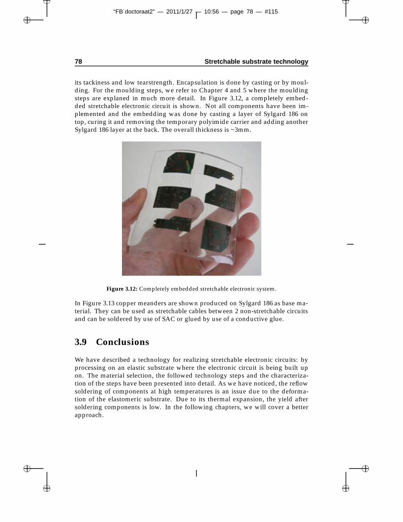
“FB˙doctoraat2” — 2011/1/27 — 10:56 — page 78 — #115�
�
�
�
�
�
�
�
78 Stretchable substrate technology
its tackiness and low tearstrength. Encapsulation is done by casting or by moul-ding. For the moulding steps, we refer to Chapter 4 and 5 where the mouldingsteps are explaned in much more detail. In Figure 3.12, a completely embed-ded stretchable electronic circuit is shown. Not all components have been im-plemented and the embedding was done by casting a layer of Sylgard 186 ontop, curing it and removing the temporary polyimide carrier and adding anotherSylgard 186 layer at the back. The overall thickness is ~3mm.
Figure 3.12: Completely embedded stretchable electronic system.
In Figure 3.13 copper meanders are shown produced on Sylgard 186 as base ma-terial. They can be used as stretchable cables between 2 non-stretchable circuitsand can be soldered by use of SAC or glued by use of a conductive glue.
3.9 Conclusions
We have described a technology for realizing stretchable electronic circuits: byprocessing on an elastic substrate where the electronic circuit is being built upon. The material selection, the followed technology steps and the characteriza-tion of the steps have been presented into detail. As we have noticed, the reflowsoldering of components at high temperatures is an issue due to the deforma-tion of the elastomeric substrate. Due to its thermal expansion, the yield aftersoldering components is low. In the following chapters, we will cover a betterapproach.

“FB˙doctoraat2” — 2011/1/27 — 10:56 — page 79 — #116�
�
�
�
�
�
�
�
3.9 Conclusions 79
Figure 3.13: Stretchable cables made on stretchable substrate.

“FB˙doctoraat2” — 2011/1/27 — 10:56 — page 80 — #117�
�
�
�
�
�
�
�
References
[1] D. Kim, J. Xiao, J. Song, Y. Huang, J. Rogers. Stretchable, Curvilinear Elec-tronics Based on Inorganic Materials. Advanced Materials, 22(19):2108–2124,May 18 2010.
[2] I.M. Graz, D.P.J. Cotton, S.P. Lacour. Extended cyclic uniaxial loading ofstretchable gold thin-films on elastomeric substrates. Applied Physics Letters,94(7):071902 (3 pp.), 16 February 2009.
[3] S.P. Lacour, J. Jones, Z. Suo, S. Wagner. Design and performance of thinmetal film interconnects for skin-like electronic circuits. IEEE Electron DeviceLetters, 25(4):179–181, Apr 2004.
[4] P. Mandlik, S.P. Lacour, J. Li, S. Chou, S. Wagner. Fully elastic intercon-nects on nanopatterned elastomeric substrates. IEEE Electron Device Letters,27(8):650–652, Aug 2006.
[5] T. Loher, R. Vieroth, M. Seckel, A. Ostmann, H. Reichl. Stretchable electronicsystems for wearable and textile applications. In 2008 IEEE 9th VLSI Packag-ing Workshop in Japan, pages 9–12, 2008 2008.
[6] T. Loher, M. Seckel, R. Vieroth, C. Dils, C. Kallmayer, A. Ostmann, R. As-chenbrenner, H. Reichl. Stretchable electronic systems: realization and appli-cations. In 2009 11th Electronics Packaging Technology Conference (EPTC 2009),pages 893–8, 2009 2009.
[7] D. Khang, J. Rogers, H. Lee. Mechanical Buckling: Mechanics, Metrology,and Stretchable Electronics. Advanced Functional Materials, 19(10):1526–1536,May 22 2009.
[8] B. Schmied, J. Guenther, C. Klatt, H. Kober, E. Raemaekers. STELLA -STretchable ELectronics for Large Area applications - A new technology forsmart textiles. volume 60, pages 67–73, 2009. 3rd International Conferenceon Smart Materials, Structures and Systems, Acireale, ITALY, JUN 08-13,2008.

“FB˙doctoraat2” — 2011/1/27 — 10:56 — page 81 — #118�
�
�
�
�
�
�
�
REFERENCES 81
[9] Dow Corning. Technical datasheet - Sylgard 186.
[10] FRALOCK. Technical datasheet - Cirlex.
[11] Circuitfoil. http://www.circuitfoil.com.
[12] Dow Corning. Technical datasheet - OS1200 adhesion promoter.
[13] Nitto Denko. Technical datasheet - Differential DC/T 64390.
[14] Rohm and Haas. http://www.rohmhaas.com.
[15] AZ Electronic Materials. Technical datasheet - AZ 4500 Series Photoresists.

“FB˙doctoraat2” — 2011/1/27 — 10:56 — page 82 — #119�
�
�
�
�
�
�
�
Chapter 4
Peelable technology
This chapter describes a technology for the realization of stretchable electronic circuits byuse of a temporary carrier where the electronic circuit is being built up on. In the end,it is embedded into a stretchable polymer. The first section gives a general overview ofthe optimized process flow and the following sections describe the choices made and theoptimization of the individual processing steps in more detail.
4.1 Introduction
The initial technology for achieving a stretchable electronics circuit being deve-loped at CMST was based on electroplating gold meander tracks on a copper foil[1]. The gold metal tracks are embedded into a stretchable polymer by partly em-bedding the sample with PDMS, etching the supporting copper and embeddingthe exposed side, resulting in a stretchable electronics substrate (Figure 4.1). Thin,typically 4 μm, fine-pitch, typically (starting from) 15 μm wide meandered tracesare possible due to the additive nature of the processflow (electroplating) lead-ing to very dense electronic circuits (Figure 4.2). Elastic interconnections weredeveloped which could be stretched between 50% and 100% in the longitudinaldirection without influencing their resistance. This technology is very suitablefor applications where biocompatibility is of major importance (Au is inert to allchemicals it encounters inside the body). Besides these features, the approachhas some drawbacks. While processing, all metal tracks are short circuited. Thiscan give problems when embedding batteries. Furthermore, the copper substrateused as temporary carrier needs to be etched completely in the end, loweringdown the environmental friendliness of this process. These problems can besolved by the approach presented in this chapter.

“FB˙doctoraat2” — 2011/1/27 — 10:56 — page 83 — #120�
�
�
�
�
�
�
�
4.2 General description of process flow 83
Figure 4.1: Au-plating technology process flow for achieving stretchable electronic cir-cuits.
Figure 4.2: Au-plated meanders on copper substrate. Typical feature size: 90 μm width, 4μm height.
4.2 General description of process flow
A general overview of the process flow developed during this PhD study isshown in Figure 4.3 and 4.4. A copper foil is laminated on a rigid/flexible carrier

“FB˙doctoraat2” — 2011/1/27 — 10:56 — page 84 — #121�
�
�
�
�
�
�
�
84 Peelable technology
by use of a temporary adhesive. By lithography and etching, the copper patternsare formed realizing the stretchable interconnections. Soldermask is applied onthe areas where components are mounted and the copper is foreseen of a finish toenhance solderability. Components are mounted and soldered leading to a func-tional circuit. At this stage, after testing and eventually reparation, the circuit isready to be transferred into a polymer.
CopperA
Copper
SubstrateWaxB
C
Photoresist application
Illumination & developing
D
Etching & stripping
Soldermask
E
F
Suface finish (OSP)
G
Soldering components
H
Figure 4.3: Peelable technology process flow - substrate fabrication.

“FB˙doctoraat2” — 2011/1/27 — 10:56 — page 85 — #122�
�
�
�
�
�
�
�
4.2 General description of process flow 85
Putting into mold
Primer
I
Putting into mold
Filling mold with PDMS & curing
J
Filling mold with PDMS & curing
K
Unmold bottom mold & peeling of substrate
L
Strip wax
M
Filling mold with silicone & curing
N
Unmolding
O
Figure 4.4: Peelable technology process flow - substrate moulding.

“FB˙doctoraat2” — 2011/1/27 — 10:56 — page 86 — #123�
�
�
�
�
�
�
�
86 Peelable technology
Before embedding, an adhesion promotor is applied. This in order to have agood adhesion between the components, tracks, soldermask and the polymer.In the case moulding is used, the substrate is put into a mould where PDMSis injected on top of the circuit by liquid injection moulding. After heatcuringthe polymer, the bottom mould is removed. The temporary carrier can then beremoved by dissolving/melting the temporary adhesive followed by a cleaningstep to remove this temporary adhesive. Adhesion promotor is applied on theback side, the bottom mould is replaced and PDMS is injected. After fully curing,the mould is opened and the completely PDMS embedded stretchable electroniccircuit can be removed. More details about this process flow and its optimizationwill be in detail explained in the following sections.
4.3 Lamination of copper on carrier with temporaryadhesive
4.3.1 Copper type
The used copper foil in Figure 4.3(A) has been selected in order to have a goodadhesion between the copper foil and the rigid/flexible carrier by use of the tem-porary adhesive. The good adhesion should be maintained during all the processsteps. This is achieved by selecting a copper sheet, used for the fabrication oflaminates for rigid composite and conventional multi-layer/mass lamination ap-plications. This means, a copper sheet with a certain roughness at the interfaceside and a rather smooth surface at the patterning side. Furthermore, the me-chanical properties of the copper foil are important, this because the copper willbe subjected to mechanical forces. For these reasons, a TW-YE 18 μm copper foil(Circuitfoil [2]) has been used to demonstrate the feasibility and characterize theprocess flow. The properties of the copper foil are shown in Table 4.1. The un-treated side of the copper has a roughness between 0.2-0.4 μm (=the side we willuse for photodefinition), on the treated side it’s between 6μm-8μm (the side wewill use for having a good mechanical adhesion to the temporary substrate). Theinorganic, so-called YE protection on the shiny surface of the foil offers superiorresistance to oxidation in warm and humid environments.
Parameter ValueUntreated side roughness 0.20µm - 0.40µm
Treated side roughness 6µm - 8µmTensile strength transverse at RT 276 MPa
Elongation transverse at RT 6%
Table 4.1: Properties of TW-YE copper foil.

“FB˙doctoraat2” — 2011/1/27 — 10:56 — page 87 — #124�
�
�
�
�
�
�
�
4.3 Lamination of copper on carrier with temporary adhesive 87
4.3.2 Temporary adhesives
The copperfoil is laminated by use of a temporary adhesive on the rigid/flexiblesubstrate 4.3(B, C).The desired properties of the temporary adhesive include:
• Good adhesion between carrier and circuit upto 60oC (= temperature of Cuwet-etching process).
• Being non tacky when exposed in order to avoid dust collection, adherenceto screen during screenprinting,..
• Compatible with acid etching, base developing/stripping, solvents,.. thusall chemicals involved in the process.
• Non-burning and removable after a temperature step of 260oC.
• Having a bad adhesion to PDMS when its surface is treated with PDMSprimer. Otherwise the temporary carrier won’t be removable anymore afterthe first moulding step.
We come back to these issues during the following sections. To find a temporaryadhesive fullfilling all these needs was not easy. Different kinds of materialshave been studied. The feasibility of every solution is discussed in the followingparagraphs:
Pressure sensitive adhesives
To form a permanent bond, structural adhesives harden via processes such asevaporation of solvent, reaction with UV radiation, chemical reaction (such astwo part epoxies), or cooling (as in hot melts). In contrast, pressure sensitive ad-hesives (PSAs) form a bond simply by the application of light pressure to marrythe adhesive with the adherend. Pressure sensitive adhesives are designed witha balance between flow and resistance to flow. The bond forms because the adhe-sive is soft enough to flow, or wet the adherend. The bond has strength becausethe adhesive is hard enough to resist flow when stress is applied to the bond.PSAs are usually based on an elastomer compounded with a suitable tackifier.The strength of the bond, for PSAs expressed as the shear holding power, is de-termined by the type and ratio of the base polymer and tackifier and the level ofcross-linking of the polymer [3],[4],[5]. The idea behind this option was to usean adhesive that shouldn’t be removed by using a solvent rinse after mouldingthe top part of the circuit. With the other solutions that will be proposed, youalways have a cleaning step in order to remove it completely. By use of a pressure

“FB˙doctoraat2” — 2011/1/27 — 10:56 — page 88 — #125�
�
�
�
�
�
�
�
88 Peelable technology
sensitive silicone, no residues are left after removing the temporary carrier. Thisoffers a great advantage.
Gel silicones Sylgard 527 and Sylgard 4150Sylgard 527 [6] and Sylgard 4150 [7] are primerless silicone dielectric gels. Theyare two component, transparent silicone encapsulants specially designed to seal,protect and preserve the electrical characteristics of delicate electronic circuitsin severe environments. The products cure in place to form a cushioning, self-healing, resilient gel-like mass. They both exhibit a reformable, pressure-sensitiveadhesive bond to many compatible substrates. These materials are typicallyuncross-linked or slightly cross-linked mixtures of a high molecular weight poly-mer with a tackifier resin, though in some systems the tackifier resin is omitted.The adhesive normally has a glass transition temperature of 20oC to 50oC belowthe temperature of usage, so is essentially a rubbery liquid. Both silicones havebeen applied on a substrate and cured. The main disadvantage is that the surfaceremains somehow tacky, this will give problems in terms of dust collection andadhesion to the screen during screenprinting soldermask, solderpaste. Further-more, the adhesion itself of the copper structures to the gel-silicone interface wasnot high enough.
Flex fixer boardA flexfixer board [8] is used as carrier for flexible substrates. It is suitable for sur-face mount technology (SMT), solder paste printing, encapsulation or underfilldispensing and during reflow and curing processes. The base of the board can beordered in various thicknesses. Usually, standard thickness is 1.6mm and basesubstrates can be manufactured from FR4, G-10, magnesium, aluminium. Theresin is a film applied to the base and is used to hold the flexible circuits in placeand flat. The resin will hold the flex circuit during the entire assembly process.At the end of the process the circuits can be peeled off, no residue will be lefton the circuits. A copper foil has been laminated but it was immedeately clearthat the adhesion of the copper structures to the board was not high enough:delamination was observed during copper etching.
Double sided tape Nitto DenkoThis tape Nitto 64390 is a differential pressure sensitive tape [9] been developedfor application of flexible substrates on carriers during processing and has beenoptimized to be able to withstand reflow soldering temperatures. It consists of apressure sensitive acrylic adhesive (38 μm) on the permanent side and a pressuresensitive acrylic adhesive (25 μm) on the removable side. In between, there is aPET carrier (12 μm). Is serves for temporary bonding of various substrates whoneed to be removed from each other without leaving any residue. A drawback ofthis tape is that it sticks, thus during processing it will give problems in terms ofdust collection and adhesion to the screen during screenprinting soldermask or

“FB˙doctoraat2” — 2011/1/27 — 10:56 — page 89 — #126�
�
�
�
�
�
�
�
4.3 Lamination of copper on carrier with temporary adhesive 89
solderpaste. Furthermore, the adhesion itself of the copper structures to the tapewas not high enough.
Photoresists as adhesion layer
Another idea was to use a photoresist layer as adhesive layer between the copperand another substrate. Photoresist has been optimized to have a good adhesionwith copper, can be easily stripped in a stripper solution and doesn’t stick duringprocessing. Attention should be paid to the fact that the photoresist acting as theadhesive layer doesn’t dissolve during developing or stripping the photoresistused for the pattern definition of the copper. Another issue needed to be testedwas the possibility of stripping the photoresist adhesion layer after vapour phasesoldering.
Dry film photoresist FX Riston 930FX Riston 930 [10] is a negative working, aqueous processable dry film pho-toresist suitable for print-and-etch and tent-and-etch applications with acid andalkaline etchants. It has a very high resolution capability with wide processinglatitude. The thickness is 30 μm and is applied by lamination using a roll lamina-tor. A micro-etched 18 μm TW-YE copper sheet has been used where the roughside was foreseen of 3 layers of FX Riston 930 photoresist by roll laminating ata temperature of 120oC. 3 layers are used in order to reach a thickness givingenough mechanical strength to act as supporting layer. The photoresist has aprotective sheet and is removed before every new laminating step. In this way,a final photoresist thickness of 90 μm has been achieved. On the smooth sideof the copper, 1 layer of FX Riston 930 was foreseen, being used to pattern thecopper. This side was photo-illuminated and patterned through a glass mask.Also the backside was illuminated in order to make it resistant to the 1% Ca2CO3
developer solution. Nitto 64390 double sided tape is used to attach the sample toa ceramic for the subsequent wet processing steps. The copper has been etchedand the top photoresist stripped by use of 0.8% NaOH solution. The result ofthese process steps is shown in Figure 4.5 and 4.6. The photoresist at the backsideis also attacked by the stripper solution but due to the thickness (60 μm) this isnot a problem.A similar sample was made for testing the vapour phase soldering resistance.The same design has been used as shown in Figure 4.11. It was observed thatthe photoresist didn’t withstand the vapour phase temperature and started todeform. Furthermore, delamination of the copper structures was observed asdepicted in Figure 4.7.

“FB˙doctoraat2” — 2011/1/27 — 10:56 — page 90 — #127�
�
�
�
�
�
�
�
90 Peelable technology
Figure 4.5: FX Riston as adhesive/carrier and photoresist for copper etching: after etchingcopper.
Figure 4.6: FX Riston as adhesive/carrier and photoresist for copper etching: after strip-ping top photoresist.
Figure 4.7: FX Riston as adhesive/carrier and photoresist for copper etching: before (a)and after (b) vapour phase soldering.

“FB˙doctoraat2” — 2011/1/27 — 10:56 — page 91 — #128�
�
�
�
�
�
�
�
4.3 Lamination of copper on carrier with temporary adhesive 91
Spin-on photoresist AZ4562AZ4562 [11] is a thick positive photoresist, intended for applications where coa-ting thicknesses above 3 μm are required. We applied it by spincoating on therough side of a 18 μm TW-YE copper sample at 2000 rpm, resulting in a layerthickness of ∼10 μm. A hardbake step was performed in a convection oven at120oC during 30 minutes. Copper patterning was done using the dry film pho-toresist FX Riston 930 and wet etching. After application of the photoresist byroll lamination, the sample was placed on a ceramic with the Nitto 64390 dou-ble sided tape. The AZ4562 photoresist is not strong enough to act as a carrierduring the wet processing steps. After etching, it was already observed that thestrength of the AZ4562 photoresist was not high enough and some parts of it al-ready delaminated (Figure 4.8 a). Vapour phase soldering was performed (Figure4.8 b) but the quality of the sample was already too low before so this option wasdiscarded.
Figure 4.8: AZ4562 photoresist as adhesive: before (a) and after (b) vapour phase solder-ing.
Waxes
Waxes can be characterized by the following properties [12]:
• Solid at room temperature (soft and flexible to brittle and hard).
• Melting point above 40oC.
• Low viscosity just above melting point.
• Natural or synthetic origin.
• Consistency and solubility are strongly dependent on temperature.
• Can be polished under slight pressure.

“FB˙doctoraat2” — 2011/1/27 — 10:56 — page 92 — #129�
�
�
�
�
�
�
�
92 Peelable technology
The fact that they are solid at room temperature, especially non-tacky, make themideal for our application. When they are melted, they can be applied and usedas adhesive, as long as they aren’t subjected to temperatures above the meltingpoint and emersed in mediums that dissolve them. Different types of waxes arecompared below.
Aquabond water soluble waxAquabond’s water soluble thermoplastic [13] is designed for temporary moun-ting of hard materials for slicing, dicing, grinding, lapping and polishing, andworks well as a chemical etch barrier. Aquabond comes in 3 different bondingtemperatures. ABS-85 has been tried, having the highest melting temperature of85-105oC. The other properties are listed in Table 4.2. It has been applied on therough side of a 18μm TW-YE copper sheet. This by heating up the copper on thehotplate of a doctorblade upto 120oC and applying a layer of this wax by castingusing the blade (Figure 4.9).
Parameter ValueTacking temperature 50-60oC
Softening temperature 60-85oCMelting temperature 85-105oCBonding temperature 85-105oC
Viscosity (75oC) <3000 cpsWater Solubility (80oC) 100%
Debond/Cleanup Hot DI Water
Table 4.2: Properties of Aquabond ABS-85 water soluble wax.
Figure 4.9: Application of Aquabond wax on copper sheet by doctorblading.
A thickness of 100 μm has been chosen. The sample has been manually appliedon an etched RO4003 ([14]) substrate by pressing such a substrate on the heatedcopper sheet with molten wax. When the sample is back at room temperature,the wax hardens again. The copper has been patterned by use of a dry film pho-toresist (FX Riston 930 [10]) and wet etching. During wet etching of the copperat 65oC, no delamination has been observed of the patterns (Figure 4.10). Next,

“FB˙doctoraat2” — 2011/1/27 — 10:56 — page 93 — #130�
�
�
�
�
�
�
�
4.3 Lamination of copper on carrier with temporary adhesive 93
the sample was put into the vapour phase soldering station resulting in a goodsoldered thin small-outline package (TSSOP) (Figure 4.11 a) but during solder-ing, it has been observed that the wax started to burn (Figure 4.11 c). It was notremovable anymore and PDMS Sylgard 186 didn’t cure anymore on it. Therefore,this option has been discarded.
Figure 4.10: Result after copper etching: no delamination observed by use of Aquabond85.
Figure 4.11: (a) Before vapour phase soldering, after application of solderpaste and TSSOPpackage. (b) After vapour phase soldering, well soldered TSSOP package. (c) After vapourphase soldering, Aquabond wax is burnt (brown color).

“FB˙doctoraat2” — 2011/1/27 — 10:56 — page 94 — #131�
�
�
�
�
�
�
�
94 Peelable technology
Quickstick T135 waxThis is a crystal clear wax [15] and has a high hardness and strength. This tempo-rary mounting wax is used in a variety of applications to bond samples duringprocessing. It has been developed for diamond wheel cutting, wire saw cutting,abrasive slurry cutting, ultrasonic cutting, lapping and polishing, etc. This waxis soluble in acetone and methylene chloride, but resists most other commonsolvents. It’s a thermoplastic polymer with a softening point of 71oC and flowpoint of 135oC. The viscosity at flow point is 6000 cps. It has been tested in asimilar way as the Aquabond wax. This wax resisted all chemicals used duringprocessing and was removable after vapour phase soldering! This wax will befurther described in the following sections and is the main option for use in thestretchable circuit technologies.
To conclude this section, several materials have been tested and compared, somewith more success than others. In the technologies that will be presented, Quick-stick 135 is the best option and will be used because it gives good adhesion duringprocessing, even during wet etching at 65oC. It’s compatible with all the chemi-cals used and it doesn’t stick at room temperature, a necessity for screenprintingsoldermask or solderpaste. It also doesn’t stick with the adhesion promotor weuse in order to get good adhesion between the PDMS and the circuit structures.A drawback is the way of application and the needed removal rinse in the endof the process. By use of alternative process techniques, the issues we have withsome materials could be solved. E.g. by laminating soldermask and dispense sol-derpaste, the tackiness of the surface becomes less critical. Concerning adherenceto the embedding elastomer after application of the primer on the adhesive, ifone would use other embedding materials than silicone (e.g. polyurethane), thisissue would disappear. During this work, we will focus on the use of Quickstick135 wax.
4.3.3 Temporary substrate
In the beginning, a flexible substrate has been used as carrier. A flexible substrateoffers the advantage of being compatible with roll-to-roll processes. Also, pee-ling off the temporary carrier after the first moulding step (see further) is easiercompared to a rigid carrier. A copper etched Upisel SE1410 foil [16] has beenused for these purposes: adhesion experiments showed that the adhesion be-tween a smooth polyimide film, Quickstick T135 and a copper sheet was not highenough. Therefore, an etched Upisel SE1410 foil has been used, having a certainroughness at the interface and allowing a good physical adhesion. In Figure 4.12a, the peeling off of such a substrate is shown at the end of the fabrication process.Due to impractical reasons, mainly because of handling, the change was made toa rigid carrier. This makes the manual processing much easier during the PCB

“FB˙doctoraat2” — 2011/1/27 — 10:56 — page 95 — #132�
�
�
�
�
�
�
�
4.3 Lamination of copper on carrier with temporary adhesive 95
process steps. In this way, the production of our stretchable circuit technologycomes closer to standard, rigid PCB production steps what is favorable. Anetched RO4003 substrate (Rogers [14]) was chosen, having a glass transition tem-perature of 260oC and thus, able to withstand a vapour phase reflow solderingprocess. In a later stage of the process development, an etched FR4 board hasbeen used. In Figure 4.12 b, the RO4003 carrier (Rogers [17]) is shown.
Figure 4.12: Temporary carriers: (a) flexible and (b) rigid.
4.3.4 Lamination
The wax is deposited on the roughest side of the copper, to ensure maximumadhesion of the copper to the temporary substrate. The wax is used as a tem-porary adhesive which looses its adhesion when heated (melting point is 135oC)or when dissolved in acetone. The wax is applied by dissolving one Quickstick(13.5 g) in 30 ml of acetone and spin coating it on the copper and the temporarysubstrate. Spinning is done at 1000 rpm during 30 secs. The copper is thenlaminated on the flexible substrate in a Lauffer vacuum lamination press. Thetemperature and pressure profile for vacuum lamination is shown in Figure 4.13.The temperature is increased from 50oC upto 75oC. In this way, the wax startsto melt. After 10 minutes, when the wax has become tacky, pressure is appliedfollowed by lowering the temperature.
In this way, laminated samples are obtained as illustrated in Figure 4.14.These rigid samples can be handled as conventional PCB substrates ready forfurther processing. 18 μm TW-YE copper has been chosen resulting in achievablelinespacing/trackwidth of 50 μm/50 μm. The sheet can easily be replaced byanother, thinner/thicker copper foil depending on the application (see WirelessPower Circuit demonstrator in Chapter 7). The minimal copper thickness weused was 9 μm, to obtain small features for e.g. high-density electronic circuits.

“FB˙doctoraat2” — 2011/1/27 — 10:56 — page 96 — #133�
�
�
�
�
�
�
�
96 Peelable technology
Figure 4.13: Vacuum lamination profile.
Figure 4.14: Vacuum lamination of TW-YE copper samples on etched RO4003 substrate.
4.3.5 Adhesion of copper on carrier
To determine the effect of certain process paramaters on the adhesion of the cop-per on the temporary carrier, peeltests on different samples have been performed.2 types of copper have been used, having a different roughness. For TW-YE, it is6μm - 8μm, for plain copper it is ∼2 μm. This to have a clue of the importance ofthe roughness of the copper on the adhesion. 2 ways of lamination of the copperon the sample have been used. A first way by spinning wax on the copper and on

“FB˙doctoraat2” — 2011/1/27 — 10:56 — page 97 — #134�
�
�
�
�
�
�
�
4.3 Lamination of copper on carrier with temporary adhesive 97
the substrate and vacuum lamination during 30 minutes according to the profileas shown in Figure 4.13. A second way by spinning wax on the substrate and rolllamination the copper onto it by use of a roll laminator. The configuration of theroll laminator is depicted in Table 4.3. 3 different wax solutions have been made:15 ml, 30 ml and 60 ml acetone per Quickstick (13.5g). This in order to determinethe effect of wax concentration on the adhesion.
Parameter ValueLaminator type MegaElectronics Photopolymer Dry Film Laminator
Temperature 140oCLamination speed 0.15 meters / min.Pressure setting 1/16th inch thick panels to 3/32nd inch thick panels.
Table 4.3: Settings of roll laminator.
For all the samples, peelstrength tests have been performed. This by lasercutting3 mm wide strips after lamination of the copper on the substrate. A sample isshown in Figure 4.15 mounted into the peelstrength test setup.
Figure 4.15: Peeltest sample in test setup.
The results of these tests are shown in Table 4.4 and Figure 4.16 where the peel-strength is expressed in N/mm.
15 ml 30 ml 60 mlTW-YE copper 0.57 N/mm 0.64 N/mm 0.34 N/mmPlain copper 0.78 N/mm 0.69 N/mm 0.35 N/mm
TW-YE copper, roll laminated 0.47 N/mm 0.32 N/mm 0 N/mm
Table 4.4: Peelstrength test results.
For the value of 0 N/mm, the adhesion was too low to do proper peelstrengthmeasurements.

“FB˙doctoraat2” — 2011/1/27 — 10:56 — page 98 — #135�
�
�
�
�
�
�
�
98 Peelable technology
Figure 4.16: Peelstrength test results.
The following conclusions can be made out of the data:
• Adhesion of wax solution based on 30 ml acetone is twice as good than fora 60 ml solution. The effect on adhesion is much more expressed betweenthe 30 ml and 60 ml based solution than between the 15 ml and 30 ml basedsolution.
• No big difference in adhesion between TW-YE and plain copper: roughnessis less important than expected.
• The adhesion of the roll laminated samples is half the adhesion strength ofthe vacuum press laminated samples in the case of a 30 ml based solution.
• The adhesion of the roll laminated samples by use of the 60 ml solution, isnot sufficient to perform peelstrength tests.
Out of these experiments, we concluded to work further with the TW-YE type ofcopper foil. The roughness of the copper on the backside will play an importantrole in the technologies presented in the upcoming chapters where adhesion tothe supporting polymer is of major importance. A wax solution of 1 stick per 30ml is used giving more or less the same adhesion compared to the 15 ml solution.Furthermore, dissolving the stick in 30 ml is easier, as is the spincoating of a lessviscous material. The presented vacuum lamination cycle will be further used,

“FB˙doctoraat2” — 2011/1/27 — 10:56 — page 99 — #136�
�
�
�
�
�
�
�
4.3 Lamination of copper on carrier with temporary adhesive 99
due to its proven functionality.
After lamination of the copper on the carrier, a lithography step takes place.The temperatures of the soft- and postbake steps mentioned in the datasheet ofAZ4562, are quite high and we risk the loss of adhesion between the copper andsubstrate (due to wax melting). In order to verify this, copper laminated base sub-strates were compared by processing a number of samples at the recommendedlithography temperatures and at lowered lithography temperatures. Part of theused copper mask design is shown in Figure 4.17, consisting of parallel rows ofmeanders varying in width from 56 μm upto 136 μm. The remaining of the maskcontains a repitition of these structures. The parameters of the process steps arelisted up in Table 4.5.
Figure 4.17: Part of Cu wet etching adhesion test design.
Normal temperature Lowered temperaturePrebake 90 o , 2 minutes on hotplate 60 o , 15 minutes on hotplatePostbake 120 o, 30 minutes in convection oven 60 o , 15 minutes on hotplate
Table 4.5: Parameters for lithography of peelable samples using AZ4562.
Spray etching tests were performed to see the effect of the temperature steps du-ring the lithography on the adhesion of patterned meanders.The samples were etched by use of a spray etcher and an etch solution based onCuCl2, H2O2, HCl (32%) and DI water. In Figure 4.18 the results are shown fromTW-YE copper samples being processed at normal lithography temperatures (Fi-gure 4.18 a) and TW-YE copper samples being processed at lowered temperatures(Figure 4.18 b). Qualitatively, we see a clear difference between the samples.Lowering the lithography temperatures is necessary in order to keep the goodadhesion between the tracks and the substrate. Non of the samples with loweredprocessing temperatures didn’t show any delamination.

“FB˙doctoraat2” — 2011/1/27 — 10:56 — page 100 — #137�
�
�
�
�
�
�
�
100 Peelable technology
Figure 4.18: Spray etch tests to measure adhesion performance: (a) Normal lithographytemperatures. (b) Lowered lithography temperatures.
4.4 Patterning of copper
4.4.1 Micro-etching
Before the application of a photoresist, the surface of copper has to be preparedfor cleanliness and good adhesion. Inadequate adhesion may result in resist de-lamination during spray etching of the copper. Preposit-Etch E25/29 (Shipley) isused as a micro-etchant for our surface preparation. The etch rate is 0.5 μm/minAfter 2 minutes of Preposit Etch E25/29, substrates are rinsed immediately in10% HCl solution during 1 minute, followed by a 1 minute rinse in DI water. TheHCl rinse is mandatory as there are always Cu+ and Cu2+ ions left on the foilsurfaces after the microetch, which cannot be removed by immediate rinsing inDI water.
4.4.2 Photoresist application
Photoresist AZ4562 [11] (AZ-Electronic Materials [18]) is spun onto the copperand pattern definition is done by standard lithography. The spin speed is 2000rpm, resulting in a ∼10μm thick photoresist layer. After a softbake at 60o C du-ring 15 mins, the photoresist is illuminated during 22,5 secs under a 8 mW/cm2
UV lamp, using a dedicated glass mask. We develop the samples in a 1:1 solutionof Microposit Developer and DI water. Developing time is 2 mins. After deve-lopment, the photoresist is hard baked on a hotplate during 15 mins at 60oC. Thesoftbake temperature has been lowered from 90oC mentioned in the datasheetto 60oC. The hardbake temperature has also been lowered from a recommended120oC in a convection oven to 60oC on a hotplate. This is necessary in order toavoid melting of the wax resulting in a bad adhesion of the copper (see previoussection). The parameters were shown in Table 4.5.

“FB˙doctoraat2” — 2011/1/27 — 10:56 — page 101 — #138�
�
�
�
�
�
�
�
4.4 Patterning of copper 101
4.4.3 Copper spray etching
An etching step takes place to define the copper tracks of the electronic circuit.For stripping the photoresist, non-diluted AZ400K [19](AZ-Electronic Materials[18]) developer is used being compatibille with the wax. In this way, coppertracks are obtained being attached with the wax to the temporary substrate. Iso-Propanol Alcohol (IPA) has also been tested for stripping the photoresist, but thetime to strip the photoresist was too long and the result was not always satisfy-ing. The photoresist was not completely removed even after several minutes ofemersion.
Also, a characterization of the copper etching of the TW-YE copper laminatedsamples, was performed. This in order to determine the minimal feature sizesand underetch. Samples were prepared by use of the parameters mentionedin the previous sections. A dedicated mask design was used containing mean-ders varying in width. In Figure 4.19, part of the design is shown after etchingshowing the meander tracks going from 56 μm upto 136 μm width defined onthe mask. Samples were made and processed while measuring the features af-ter every process step. The dimensions of the patterns on the glass mask werecompared with the dimensions of the photoresist after development and the di-mensions of the copper tracks after spray-etching. On one of the samples made,the variance in width of the tracks within a sample was studied in order to get anaverage width of the different tracks. To minimize the amount of measurements,for the other samples only a few measurements were done to check if the trackwidths are in the same range as the other measured samples. This was confined.
Figure 4.19: Spray etched sample containing meander tracks with different widths.

“FB˙doctoraat2” — 2011/1/27 — 10:56 — page 102 — #139�
�
�
�
�
�
�
�
102 Peelable technology
The conclusions we could draw out of the measurements are:
• The average difference in width between the track width definition on themask and the track definition of the photoresist for a first sample is 6,2 μm.
• The average difference in width between the track width definition on themask and the track definition for a second sample is 6,6 μm.
• The average underetch for that first sample is 12,7 μm (underetch = differ-ence between photoresist width and copper track width).
• The average underetch for that second sample is 10,3 μm.
• The average difference in track width between mask and copper patterndefinition is 18,8 μm for that first sample (12,7 μm + 6,2 μm).
• The average difference in track width between mask and copper patterndefinition is 16,94 μm for that second sample (10,3 μm + 6,6 μm).
In Figure 4.20, it is shown what happens with the profiles of the different layers(copper, photoresist) during the different process steps.
Figure 4.20: Profiles of different layers during copper patterning (dimensions in μm).
In this way, the underetch can be taken into account during the mask designs.
4.5 Application of soldermask
Similar to conventional PCB or FCB substrate processing, soldermask can be ap-plied. This soldermask forms a permanent protective coating and prevents brid-ging between conductors by solder. This is done by screenprinting ELPEMERSD2463 FLEX HF on the samples. Curing temperatures and time were optimizedto avoid melting of the wax and mixing with the soldermask. Prebake was done

“FB˙doctoraat2” — 2011/1/27 — 10:56 — page 103 — #140�
�
�
�
�
�
�
�
4.6 Copper surface finish 103
at 60oC during 120 mins. Postbake was done at 150oC during 60 mins. In be-tween, illumination (250 mJ/cm2) takes place through a glass mask and deve-loping in a 1 % Na2CO3 solution. The result is a cured soldermask layer withthickness ∼20μm.
4.6 Copper surface finish
In order to have a reliable connection between the copper pads and the leads ofcomponents, several finishes have been examined.
4.6.1 No finish
Chemically clean copper is the easiest material to solder; it can be soldered witheven the mildest fluxes [20]. Unless it is protected with a protective coating, itssolderability will rapidly degenerate because of oxides (caused by oxygen in air)and tarnishes (mainly caused by chemicals in the air e.g sulfur dioxide). This op-tion has sometimes been succesfully used in cases where the soldering happenedimmediately after dipping the substrates in a 10% HCl solution in order to re-move the oxides on the copper due to oxidation of the copper during the curingstep of the soldermask (150oC).
4.6.2 NiAu-finish
Copper metal pads can be coated with a NiAu finish. The Ni prevents the diffu-sion of the copper atoms through the gold layer, causing tarnishing of its surfaceand formation of an oxide and/or sulfide layer [20]. Au is a highly solderablematerial but is extremely expensive and it rapidly dissolves in the molten solder.The main function is again protecting the copper from oxidation and it improvesthe wear resistance. The use of higher gold thicknesses can reduce solder jointreliability due to the formation of tin-gold intermetallics. In the used technology,an electroless Ni finish with an electroless Au flash is deposited on the copper.Typical thickness for the Ni deposition is a few (2-3) microns; thickness of theAu is 150nm. Ni plating happens at 90o C which leads to delamination of thecopper tracks from the temporary substrate, due to the melting of the wax. Toavoid this, attempts have been made to fix this by putting a photoresist layer onthe sample, in order to counteract the delamination of the patterned structures.Places which need to be plated are left open. In this way, a NiAu finish can beobtained. Photoresist cracking was observed and the quality of the NiAu finishwas not optimal. Therefore, the conclusion has been made that this finish is notapplicable for our technology.

“FB˙doctoraat2” — 2011/1/27 — 10:56 — page 104 — #141�
�
�
�
�
�
�
�
104 Peelable technology
Figure 4.21: Substrate after NiAu-finish application. Cracks in the photoresist are ob-served and the quality of the finish is poor.
4.6.3 OSP-finish
For applications that do not require a long shelf life, an economical solution is theuse of an organic protective coating. Organic protective coatings must be easilyremovable and they must be compatible with the fluxes used in the printed circuitboard industry. An organic surface protection (OSP) from MEC has been testedand succesfully applied to the technology. It involves the following products, amicroetchant and the OSP itself.
MECBRITE CA-92 [21] is an acidic micro-etch cleaner specifically formulated toremove organic and inorganic soils such as fingerprints, light oils and oxidesfrom copper surfaces. It is versatile and particularly useful for copper cleaningapplications where it is essential to remove a thin layer metallic copper togetherwith oxides and organic contaminants.MECSEAL CL-5018 [22] is a heat-resistant water soluble preflux. Compared withconventional alkylimidazole type preflux, CL-5018 is less foamy and offers supe-rior heat-resistance, solder wettability and spreadability. Even in short processingtime, CL-5018 effectively forms a heat-resistant anti-tarnish coating only on thecopper surface. Since CL-5018 is easy to control, it offers excellent workabilityand safety.
The process steps to apply this OSP are:
• Emersion of substrate in MECBRITE CA-92 solution at room temperaturein order to have an micro-etched surface of 1 μm.
• Water rinse of 30 seconds.
• Water removal by warm air.
• Emersion of substrate in MECSEAL CL-5018 for 20 seconds and more at20oC - 40oC.

“FB˙doctoraat2” — 2011/1/27 — 10:56 — page 105 — #142�
�
�
�
�
�
�
�
4.7 Assembly of components 105
• Water rinse of 30 seconds.
• Water removal by warm air.
4.7 Assembly of components
Soldering, both wave and reflow, are currently by far the most standard ways ofautomated assembly of electronic components onto substrates. It is our chosenway in order to make electrical contact between the defined stretchable copper in-terconnections and the SMD components. In the past, most component assemblywas done by soldering with Pb-Sn-alloys. However, European regulation statesthat lead (Pb) must be banned from all processes, also in the electronics indus-try. Alternatives have been developed and are typically Sn-Ag-Cu-alloys (SAC).They have the disadvantage that they still require higher reflow temperatures,over 250oC instead of approximately 180oC.We have used Interflux Delphine SAC305 solderpaste alloy, consisting of a mix-ture of flux and metal solder particles. This solderpaste is lead-free and also freeof halogens, guaranteeing a high reliability. This paste has a high resistance tothe elevated temperatures inherent to lead-free processes.The solder paste can be dispensed manually or automatically on the contact padsof the substrate, before aligning and placing the components. A common problemin soldering is tombstoning. This term refers to surface mounted components,mostly small passives (resistors and capacitors), that rise up during solderingleaving one end soldered to the board and the other end free. It is caused by anunbalanced force due to non-uniform melting during reflow, mostly coming fromdifferent amounts of solder at opposite ends of the component. Therefore, auto-matic application by screenprinting or dispensing is preferred in order to haveequal amounts of solderpaste. The wax is a plane, non-sticky surface makingscreenprinting solderpaste not an issue in terms of adherence to the screen du-ring printing.A considerable advantage of soldering as compared to current adhesive assem-bly, is its self-alignment ability: during reflow, the solder makes sure the compo-nents contacts (pins) are aligned optimally to the corresponding substrate pads.This is especially the case when a soldermask is applied next to the contact pads:the soldermask repels the solder, so that it is forced onto the pads. On the down-side, soldering requires relatively high temperatures.We have used a vapour phase reflow station because of its availability at the labfacilities of CMST. By this soldering technique, the board is placed with solder-paste and components into the reflow chamber where it is exposed to the vapourphase of a boiling liquid. This liquid is inert with respect to the solder and theboard. The hot vapours begin to condense on the cooler printed circuit board,thus heating it. As the process progresses sufficient energy for sustained solder

“FB˙doctoraat2” — 2011/1/27 — 10:56 — page 106 — #143�
�
�
�
�
�
�
�
106 Peelable technology
reflow results. The solder wets to lead and pad and, as the board is removed fromthe hot vapour, the molten solder solidifies, bonding component leads to circuitboard pads. An advantage of this process is that the reflow happens in an inertatmosphere, resulting in an excellent joint quality.Figure 4.22 shows the temperature profile of the used vapour phase solderingprocess. This profile is based on the profile recommended in the datasheet of theSAC305 alloy.
150
200
250
300
Tem
p (o
C)
0
50
100
0 50 100 150 200 250 300 350 400
Te
Time( sec)
Figure 4.22: Vapour phase soldering temperature profile.
The wax melts during soldering but hardens again after soldering. The circuit istemporary laying free on the carrier. The total wax thickness is important here.When it is too thick, it’s easier for the tracks to start to float. Figure 4.23 showsthe effect of melting of the wax during soldering. Due to forces appearing duringthe hardening of the solderpaste, the tracks are shifted. This is an effect that wecertainly want to avoid. Luckily, this can be solved by use of soldermask, whichholds the tracks in their place, see Figure 4.24.
4.8 Testing and rework
A major advantage of this technology compared to technologies were the pro-cess steps take place on the elastomer, is that the electronic circuit can be testedbefore embedding. Although we try to keep up processing yields as high as pos-sible, component replacement might be necessary. Resoldering and replacementis possible without detoriating the final stretchable circuit performance.

“FB˙doctoraat2” — 2011/1/27 — 10:56 — page 107 — #144�
�
�
�
�
�
�
�
4.9 Embedding 107
Figure 4.23: Tracks shift during reflowsoldering and wax melting in absence ofsoldermask.
Figure 4.24: Soldermask preventingmovement of tracks during reflow sol-dering and wax melting.
4.9 Embedding
The substrate carrying the electronic circuit is embedded by use of an elastic ma-terial. For feasibility studies we have chosen for Sylgard 184 and Sylgard 186from Dow Corning. The properties of these silicones are mentioned in Table 4.6.
Parameter Sylgard 184 Sylgard 186Young’s modulus 0.6-2.3 MPa N/A
Viscosity 3900 mPa.sec 65000 mPa.secAppearance Transparent Translucent
Refractive index (589nm) 1.41 N/ALinear CTE 310 ppm/oC 330 ppm/oC
Hardness (durometer) A50 A24
Table 4.6: Properties of Sylgard 184 and Sylgard 186 silicone.
Embedding of the circuit in a polymer can be done by casting (doctor blading)or by moulding. Before PDMS is applied, an adhesion promotor is applied foruse with Sylgard 184 and 186. OS1200 primer from Dow Corning is applied bydipping with a wipe on the substrate. It is important to limit the applied amountof primer.
4.9.1 Casting of PDMS
In cases where a simple, flat encapsulation is needed or a very thin encapsula-tion layer, casting PDMS can be the option to embed the stretchable electroniccircuit. Well controlled layers can be applied by hand (Figure 4.25) or by useof a doctorblade (Figure 4.26). After casting the PDMS has to be cured, but thiscuring should be limited in temperature. A temperature higher than 70oC willlead to wax melting, resulting in an incurable wax-PDMS mixture. After curing

“FB˙doctoraat2” — 2011/1/27 — 10:56 — page 108 — #145�
�
�
�
�
�
�
�
108 Peelable technology
the PDMS at 50oC during 4 hours, the temporary carrier is removed. This processwill be described in the following section concerning moulding. In the end, thebackside can be casted with another layer of PDMS, again by first applying theadhesion promotor followed by another casting step.
Figure 4.25: Application of PDMS bycasting manually.
Figure 4.26: Application of PDMS bycasting using a doctorblade.
4.9.2 Moulding using PDMS
The moulding process steps are shown in Figure 4.4. First, the temporary sub-strate supporting the functional electronic circuit is put into the mould. Theupper layer of PDMS is then injected and cured. Optimal curing is done at 50oCpreventing the wax of melting and mixing with the uncured PDMS resulting inan incurable mix. Secondly, the supporting mould is removed and the temporarysubstrate is removed by heating the temporary substrate up to 200oC. In thisway, the wax melts and allows us to peel off the substrate. After release, waxresidues should be removed by rinsing in an acetone bath. Next, the backsidemould is mounted in order to inject the final layer of PDMS. After curing thislayer at 50o C during 4 hours, the system is unmoulded. The material chosen forthe moulds can be PMMA, polyetherimide ULTEM or aluminium. Each of thesematerials have advantages/disadvantages compared to each other. PMMA andULTEM are transparent, making them very suitable for silicone flow analysis.PMMA and aluminium are cheap compared to ULTEM. PMMA is not resistantto acetone, what leads to cracks in the mould when the emersion time is too long.ULTEM has a broad chemical resistance, high heat resistance and high mecha-nical strength and rigidity. We come back to the moulding steps in Chapter 5,where in more detail the mould design, the moulding and unmoulding steps willbe explained.

“FB˙doctoraat2” — 2011/1/27 — 10:56 — page 109 — #146�
�
�
�
�
�
�
�
4.10 Conclusions 109
4.10 Conclusions
We have described a technology for realizing stretchable electronic circuits byuse of a temporary carrier where the electronic circuit is being built up on. Thechoice of the materials, the different technology steps and the optimization ofeach step has been presented. A number of demonstrators will be presented inChapter 7 including a stretchable temperature sensor, an inductive link protectedby PDMS, stretchable transmission lines and antennas and a stretchable heater.These will demonstrate the feasibility of our technology process. In the followingchapters, we will come back to this technology by presenting reliability resultsand by presenting an improved version of this technology.

“FB˙doctoraat2” — 2011/1/27 — 10:56 — page 110 — #147�
�
�
�
�
�
�
�
References
[1] D. Brosteaux, F. Axisa, M. Gonzalez, J. Vanfleteren. Design and fabricationof elastic interconnections for stretchable electronic circuits. IEEE ElectronDevice Letters, 28(7):552–554, Jul 2007.
[2] Circuitfoil. http://www.circuitfoil.com.
[3] I. Benedek. Pressure-Sensitive Adhesives and Applications. Taylor and FrancisInc, 2004.
[4] J. Johnston. Pressure Sensitive Adhesive Tapes. PSTC, 2003.
[5] I. Benedek. Pressure Sensitive Formulation. VSP, 2000.
[6] Dow Corning. Technical datasheet - Sylgard 527 Technical Datasheet.
[7] Dow Corning. Technical datasheet - Sylgard 4150 Technical Datasheet.
[8] Micronsult. Technical datasheet - FlexFixer.
[9] Nitto Denko. Technical datasheet - Differential DC/T 64390.
[10] Dupont. Technical datasheet - Riston FX900 Series Dry Film Photoresist.
[11] AZ Electronic Materials. Technical datasheet - AZ 4500 Series Photoresists.
[12] C. Fillion. Shamrock Technologies - Presentation on surface modifiers.
[13] Aquabond Technologies. Technical datasheet - ABS-85.
[14] Rogers. Technical datasheet - RO4003- Woven Glass Reinforced CeramicFilled Thermoset Materials.
[15] South Bay Technologies. Technical datasheet - Quickstick MWH135 Moun-ting Wax.
[16] UBE America Inc. Technical datasheet - Polymide Base Copper Clad Lami-nate (Adhesiveless).

“FB˙doctoraat2” — 2011/1/27 — 10:56 — page 111 — #148�
�
�
�
�
�
�
�
REFERENCES 111
[17] Rogers. http://www.rogerscorp.com/.
[18] AZ Electronic Materials. http://www.az-em.com/.
[19] AZ Electronic Materials. Technical datasheet - AZ 400K Developer for AZ4500 series.
[20] Jr. C.F. Coombs. Printed Circuits Handbook, 4th edition. McGraw-Hill, 1996.
[21] MEC. CA-92 Micro-etch cleaner technical datasheet.
[22] MEC. Technical datasheet - CL-5018 Heat-resistant water soluble preflux.

“FB˙doctoraat2” — 2011/1/27 — 10:56 — page 112 — #149�
�
�
�
�
�
�
�
Chapter 5
Peelable technology withlocal polyimide support
An optimized version of the technology in Chapter 4 is presented. A layer of polyimideis introduced as support for the stretchable conductors and the functional islands. Thefirst section gives a general overview of the optimized process flow and the followingsections describe the choices made and the optimization of the individual processing stepsin more detail. Some side steps of this technology are presented including the extension todouble conductor layer circuits, reliability improvement by polyimide sandwiched metalstructures,..
5.1 Introduction
In Chapter 4, the peelable technology was presented. Some issues were reportedthat during reflow soldering, the patterns started floating onto the melted tem-porary adhesive and soldermask had to be used for holding the structures.In order to solve this, a layer of polyimide is introduced in the technology stack:the polyimide is patterned in a way that it supports the functional islands and thestretchable interconnections. This layer prevents floating of the different pads ofthe components. Furthermore, the stress during stretching is shifted to the borderof the flexible islands. The polyimide is not able to stretch and will mechanicallyprotect the soldered component connections and the straight tracks on the com-ponent islands. This principle is shown in Figure 5.1, and enhanced reliabilitywith this technology will be discussed in detail in Chapter 6.

“FB˙doctoraat2” — 2011/1/27 — 10:56 — page 113 — #150�
�
�
�
�
�
�
�
5.2 General description of process flow 113
Figure 5.1: Due to the polyimide supporting layer, mechanical stress during stretching willbe shifted from the component connection pads and the straight tracks on the functionalislands towards the border of the flexible islands.
5.2 General description of process flow
The process flow is depicted in Figure 5.2 and 5.3 and will be in detail explainedin the following sections. In comparison with Figure 4.3, the copper foil is nowfirst foreseen by patterned polyimide structures. This can be achieved by useof photodefinable polyimide or screenprinting a non-photodefinable polyimide.A curing step is needed in order to imidize the polyimide to achieve its flexibi-lity and strength. The polyimide structured copper foil is then laminated on arigid/flexible carrier by use of the temporary adhesive, Quickstick 135 wax. Bylithography and etching, the copper patterns are formed realizing the stretchableinterconnections, soldermask is applied and the copper is foreseen of a finish toenhance solderability. Components are mounted and soldered leading to a func-tional circuit. At this stage, after testing and eventually reparation, the circuit isready to be transferred into a polymer. Before embedding, an adhesion promo-tor is applied. This in order to have a good adhesion between the components,tracks, soldermask and the polymer. In the case moulding is used, the substrate isput into a mould where PDMS is injected on top of the circuit by liquid injectionmoulding. After heatcuring the polymer, the bottom mould is removed. Thetemporary carrier is removed by dissolving/melting the temporary adhesive fol-

“FB˙doctoraat2” — 2011/1/27 — 10:56 — page 114 — #151�
�
�
�
�
�
�
�
114 Peelable technology with local polyimide support
lowed by a cleaning step to remove the temporary adhesive. Adhesion promotoris applied on the back side, the bottom mould is replaced and PDMS is injected.After fully curing, the result is a completely PDMS embedded stretchable elec-tronic circuit.
Copper
Copper
Polyimide
A
BCopper
CopperP l i id
Illumination & developingC
Photoresist
Polyimide
SubstrateWax
D
E
Etching & stripping
Illumination & developing
F
Etching & stripping
Soldermask
G
H
Suface finish (OSP)
I
Soldering components
J
Figure 5.2: Process flow of polyimide supported peelable technology.
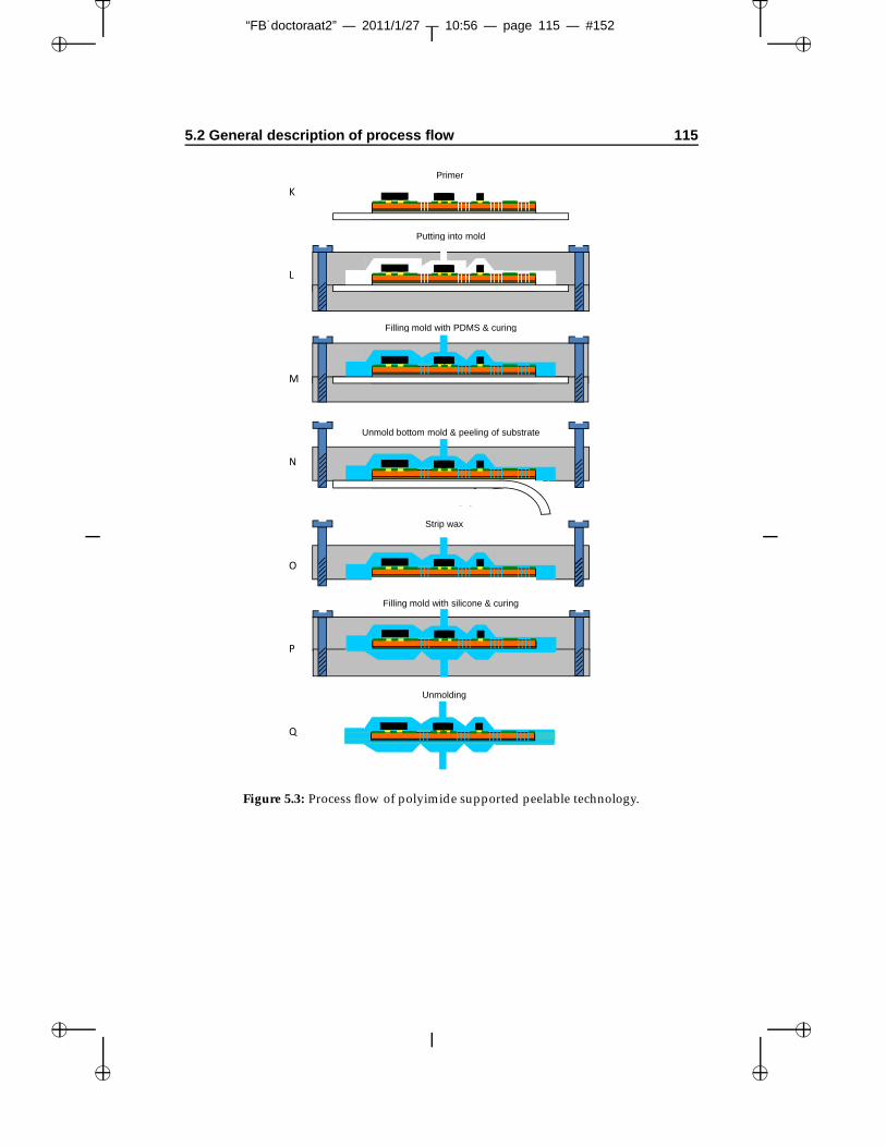
“FB˙doctoraat2” — 2011/1/27 — 10:56 — page 115 — #152�
�
�
�
�
�
�
�
5.2 General description of process flow 115
Putting into mold
Primer
K
Putting into mold
Filling mold with PDMS & curing
L
Filling mold with PDMS & curing
M
Unmold bottom mold & peeling of substrate
N
Strip wax
O
Filling mold with silicone & curing
P
Unmolding
Q
Figure 5.3: Process flow of polyimide supported peelable technology.

“FB˙doctoraat2” — 2011/1/27 — 10:56 — page 116 — #153�
�
�
�
�
�
�
�
116 Peelable technology with local polyimide support
5.3 Pattern definition of polyimide
The main goals of the polyimide are to prevent the islands from flowing on thewax during reflow soldering and to improve the mechanical robustness of thestretchable circuit. Having a flexible material below the stretchable copper inter-connections will improve the lifetime of these connections by withholding crackpropagation in the copper. The polyimide will serve as a buffer for the stressesapplied by the PDMS on the copper during stretching and the lateral stresses ofthe PDMS on the copper due to the Poisson effect. Polyimide is a suitable sup-porting material having a high Youngs modulus, being able to plastically deformover a wide elongation and being non-brittle. Furthermore at the level of the is-lands, the polyimide will improve the robustness by protecting the straight cop-per tracks and components assembled on the islands from deforming. In orderto have a support material below the copper, 2 ways of applying the polyimidehave been investigated: lithographically and screenprinting.
5.3.1 Photodefinable polyimide
By using photodefinable polyimide, islands and meander support can be ob-tained by lithographical patterning of the polyimide. 2 types have been investi-gated: PI2730 and HD4100, both from HD Microsystems [1].
The Pyralin PI 2730 [2] series have been specially developed for use as a pas-sivation layer for semiconductors and as an interlayer dielectric layer for highdensity interconnection (HDI) applications. Pyralin PI 2730 series polyamic esterscontain a negative-working photopackage making them sensitive to broadbandexposure from a mercury lamp in the range of 350 to 435 nm. The materialsare supplied as viscous solutions suitable for spin or roller coating applications.Cured film thicknesses can be achieved from 2,5 μm to 15 μm. These productsare self-priming, thus eliminating the need for an additional adhesion promoterexcept in extreme cases. The cured polyimide film offers a low dielectric constant,low coefficient of thermal expansion and good mechanical properties.
The HD-4100 Series of products [3] are new negative-tone, solvent developed,photodefinable polyimides for stress buffer and flip chip bonding applications.These polyimides were developed as self-priming, i-line sensitive, photodefin-able polyimide precursors that can be patterned to cleanly resolve micron scalerelief patterns with controlled size and wall profiles without the need for pho-toresists. HD-4100 Series products have found their greatest applicability inpackaging applications. They have excellent mechanical properties to handle thethermal and chemical extremes of post application processing, excellent elon-gation to prevent cracking, good adhesion (to underfill, UBMs, metal runners,

“FB˙doctoraat2” — 2011/1/27 — 10:56 — page 117 — #154�
�
�
�
�
�
�
�
5.3 Pattern definition of polyimide 117
etc.), smooth sloping via sidewalls and compatibility with copper (no coppermigration). They may also be used in traditional stress buffer applications.
As can be seen in Table 5.1, the CTE of PI2731 was much closer to the CTE ofcopper (∼16 ppm/oC) than the CTE of HD4100. The larger CTE mismatch willresult in some residual stress in the polyimide layers patterned on the copper byuse of the HD4100 polyimide.
Parameter PI2731 HD4100Tensile strength 180 MPa 200 MPa
Elongation >10% 45%Modulus 6.18 GPa 6.18 GPa
Coefficient of thermal expansion 13 ppm/oC 35 ppm/oCDielectric Constant 2.9 (1 KHz) 3.36 (1 MHz)
Table 5.1: Cured film properties of PI2731 and HD4100 photodefinable polyimide.
Figure 5.4: Spinspeed vs. layer thicknessof PI2731 (30 secs spintime).
Figure 5.5: Spinspeed vs. layer thicknessof HD4100 (30 secs spintime).
The spin vs. thickness curves of both polyimides are shown in Figure 5.4 and 5.5.During first process development for this technology, PI2731 was used, due to theCTE match with copper. Unfortunately, HD Microsystems stopped the produc-tion of this ’preferred’ photodefinable polyimide and we had to shift to anothervariant, HD4100. Therefore, we will report the development of the technologyby use of HD4100. To demonstrate the feasibility of the use of the HD4100 in theproposed process flow, as shown in Figure 5.6. It consists of 3 flexible islandsconnected with each other through stretchable interconnections. The islands andstretchable interconnections are supported by the photodefined polyimide layer.On places where components are, soldermask is foreseen. The design encom-passes 3 layers: for patterning polyimide, copper and soldermask.The size of the substrate is 10 by 10 cm and the processing of the polyimide willbe done starting from TW-YE copperfoil (Circuitfoil [4]). The properties of the

“FB˙doctoraat2” — 2011/1/27 — 10:56 — page 118 — #155�
�
�
�
�
�
�
�
118 Peelable technology with local polyimide support
Figure 5.6: Feasibility design for polyimide supported peelable technology: polyimide,copper and soldermask. Trackwidth = 100 μm.
copper foil were shown in Table 4.1. The polyimide is for enhanced adhesionapplied on the rough side of the copper, having a roughness between 6 μm-8 μm.Spinning is done during 10 secs at 500 rpm and 30 secs at 1500 rpm, targeting acured layer thickness of 20 μm. We softbake the polyimide on a hotplate during5 minutes at 90oC followed by 5 minutes at 110oC. To pattern the polyimide,illumination is done through a TiW patterned glass mask during 40 secs by useof an UV lamp (8 mW/cm2). Next, the polyimide is developed by use of PA400Dand PA400R (HD Microsystems). The development parameters are as follows:
• 3 minutes in PA400D
• 2 minutes in a PA400D/PA400R 1:1 solution
• 3 minutes in PA400R
• rinse with DI water brush
Full cure of the polyimide is done in a nitrogen oven with the following curingtemperature:
• heating from room temperature to 200oC, with a ramp rate of 4oC perminute
• 30 minutes at 200oC
• heating from 200oC to 375oC, with a ramp rate of 2,5oC per minute

“FB˙doctoraat2” — 2011/1/27 — 10:56 — page 119 — #156�
�
�
�
�
�
�
�
5.3 Pattern definition of polyimide 119
• 60 minutes at 375oC
• cooling down to room temperature
The processing parameters have been deducted from the recommendations men-tioned in the datasheet of the polyimide. In this way, a layer of ~20 μm polyimideon the copper is obtained. Figure 5.7 shows a sample with patterned HD4100polyimide on.
Figure 5.7: Definition of HD4100 polyimide.
Also alignment marks are defined on this polyimide layer and based on thesemarks, holes are drilled by a laser through the polyimide and copper. Theseholes are needed for alignment during copper definition at the other side. It isimportant that the copper layer definition is well aligned relative to the polyimidelayer in order that the supporting polyimide meanders are well aligned comparedto the copper meanders (Figure 5.8).
Figure 5.8: Alignment of polyimide relative to copper is important, achieved by laser-drilling alignment holes in the copperfoil.

“FB˙doctoraat2” — 2011/1/27 — 10:56 — page 120 — #157�
�
�
�
�
�
�
�
120 Peelable technology with local polyimide support
To check the reproducability of the parameters for photodefinition of the poly-imide, 3 samples were fully characterized, being processed as described. Thesamples consist of different meanders with a defined mask width of 100 μm. Af-ter development, the widths were measured. Table 5.2 shows for every samplethe different measurements along the sample. The average track width for thedifferent samples is respectively 102.69 μm (σ=2.20 μm), 104.66 μm (σ= 2.20 μm),100.57 μm (σ= 1.78 μm). The last sample has been agitated more in the 1st de-veloper solution than the others. It can be concluded that the uniformity of thedefinition across the sample is good. A profile measurement of a defined poly-imide track after curing is depicted in Figure 5.9.
Sample 1 (width in µm) Sample 2 (width in µm) Sample 3 (width in µm)101,42 104,8 102,54105,92 107,05 101,42101,42 104,8 96,91101,42 101,42 100,29104,8 107,05 101,4299,16 104,8 101,42103,67 101,42 99,16103,67 105,92 101,42
Table 5.2: Linewidths of photodefined HD4100 polyimide.
Figure 5.9: HD4100 photodefinable polyimide profile after curing.

“FB˙doctoraat2” — 2011/1/27 — 10:56 — page 121 — #158�
�
�
�
�
�
�
�
5.3 Pattern definition of polyimide 121
5.3.2 Screenprintable polyimide
As an alternative for photodefinition of polyimide, screenprinting of polyimidewas studied. In this way, the used material doesn’t need to be photodefinable.Furthermore, less material is used because of the additive nature of screenprin-ting. So far, polyimide is not so common available in screenprintable format.Most of the commercial available polyimides are for spincoating , typically usedas passivation layers for wafers or casted polyimide on copper clads. For a ma-terial to be screenprintable, it has to have the suitable rheology. The paste has tobe a non-Newtonian fluid with thixotropic properties. This means that the ide-aliter viscosity of the paste has to change in time with applied shear rate. Thechange of the viscosity is usually described by a thixotropy index. It representsthe change of viscosity between two different shear rates, usually different by afactor of 10. An example of a thixotropic material is e.g. ketchup or mayonese:in the equilibrium state they do not change their shape but when agitated theirviscosity changes rapidly. This is the reason why a paste has to roll in front of thesqueegee during printing - rolling causes the change of the viscosity of the paste.The most important properties of the different polyimides investigated for theirscreenprinting capability, are listed in Table 5.3. Most of the time, the thixotropyindex is not mentioned in the datasheet. By just the viscosity index, it’s hard topredict if a material will be screenprintable or not. For that purpose, several ma-terials have been ordered and tested to check the capability to be screenprinted.
Property/Polyimide PI2611 Q-Pilon U-Varnish A Durimide 10 Durimide 116Main solvent NMP GBA NMP NMP NMP
Solid contents (%) 13.50 27 18 N/A 11-15.5Glass transition temperature 400oC 245oC N/A N/A 371oC
Coefficient of thermal expansion 3 ppm/oC 46 ppm/oC 16 ppm/oC 52 ppm/oC 32 ppm/oCElongation 25% 9.5% 100% 74% 80%Elasticity N/A 3200 MPa 3730 MPa 3500 MPa 3300 MPa
Tensile strength 350 MPa N/A 196 MPa N/A 260 MPa
Table 5.3: Properties of selected polyimides for screenprinting.
A dedicated screen has been developed for the screenprinting tests, showed inFigure 5.10. It’s a stainless steel screen with the following characteristics:
• 400 mesh screen: 400 openings per inch
• 20 μm emulsion for NMP resistant emulsion / 60 μm for non-NMP resistantemulsion
• Angle of mesh: 45o
• Dek260 frame (23 inch by 23 inch)

“FB˙doctoraat2” — 2011/1/27 — 10:56 — page 122 — #159�
�
�
�
�
�
�
�
122 Peelable technology with local polyimide support
Figure 5.10: Dedicated screen for polyimide screenprinting purposes.
The squeegee had the following properties:
• Polyurethane 80-85 shore hardness
• Trailing edge 45o angle
N-Methyl-Pyrrolidone (NMP) resistant screens with emulsions thicker than 20μm were not available. NMP is a very aggresive solvent, attacking the standardemulsions used for covering screenprint masks.The dedicated screen contains the following test blocks:
• Vertical and horizontal lines with width of 250 μm, 200 μm, 150 μm, 100μm.
• Vertical, horizontal and diagonal meanders with width of 100 μm, 150 μm,200 μm, 275 μm.
• Full areas and areas with square holes.
• Concentric circles with different widths and pitches (Dimensions in Table5.4).
• Full area with vias having diameters of 75 μm, 100 μm, 125 μm, 150 μm, 175μm, 200 μm.
• Mesh of circles with 136 μm width and innerradius 282 μm.
In the following sections, the trials with the different polyimides will be dis-cussed.

“FB˙doctoraat2” — 2011/1/27 — 10:56 — page 123 — #160�
�
�
�
�
�
�
�
5.3 Pattern definition of polyimide 123
Circle width (µm) Pitches (µm)100 200, 300, 400, 500, 600, 700200 300, 400, 500, 600, 700, 800300 400, 500, 600, 700, 800, 900400 500, 600, 700, 800, 900, 1000500 600, 700, 800, 900, 1000, 1100600 700, 800, 900, 1000, 1100, 1200
Table 5.4: Dimensions of concentric circles on screenprinting screen.
PI2611
PI2611 [1] has a viscosity of 110-135 Poise, which is quite low. It is based onN-Methyl-2-Pyrrolidone. Screenprinting tests showed that the polyimide wasdropping through the screen and stuck the screen on the backside. This poly-imide, made for spincoating applications, is not an option. Only modifications atthe level of the material could make it screenprintable.
Q-Pilon Q-IP-GWK123
Q-Pilon Q-IP-GWK123 (PI-R&D) has a high heat resistance and good insulationproperties. The datasheet claims that a fine pattern can be directly formed by ascreenprinting method. It has been designed for application on printed circuitboards and as insulation layer film on wafers. The datasheet claims fine pro-cess ability. The product has a viscosity of 40000-50000 mPa.s and is based onγ-Butyrolactone.
Figure 5.11: Definition of Q-Pilon polyimide by screenprinting: feature size ~150 μm,thickness ~40 μm.

“FB˙doctoraat2” — 2011/1/27 — 10:56 — page 124 — #161�
�
�
�
�
�
�
�
124 Peelable technology with local polyimide support
For the experiments, the squeegee was first mounted under a 60 o angle but wechanged it to 45 o. The reason: too little material was printed. As snap off dis-tance, we started with 0.75 and moved to 1.25 mm. There was an effect but hardto describe quantitatively. Printing speed was 10 mm/second.As can be seen in the upperright picture of Figure 5.11, the material has a veryhigh viscosity and behave like a thick paste. In the picture next to it, the resultsof printing are shown. The smallest features are not printed well, the uniformityof the deposition is very small, the pattern definition is poor and the thicknessafter curing is around 40 μm (the emulsion thickness of the screen was 60 μm).The material doesn’t have the property of settling after printing and the meshpatterns remain in the printed material. We concluded that this material doesn’thave the capabilities for being screenprinted in a good way forming the supportfor the stretchable interconnects.
U-Varnish
U-Varnish (UBE [5]) is a solution of polyimide precursorpolyamic acid. It comesin two forms, U-VARNISH-A (Normal heat resistant type) and U-VARNISH-S(High heat resistant type). For our purpose, we experimented with U-VARNISH-A and performed some screenprinting tests. Some pictures are depicted in Figure5.12.
Figure 5.12: Definition of U-Varnish A polyimide by screenprinting.
As can be seen in the pictures, the viscosity of the material is too low: the mate-rial starts to flow after deposition, what makes it difficult to define good patterns.This material turned out to be not suitable for the fine pattern definition of me-anders and islands. Only modifications at the level of the material could make it

“FB˙doctoraat2” — 2011/1/27 — 10:56 — page 125 — #162�
�
�
�
�
�
�
�
5.3 Pattern definition of polyimide 125
screenprintable.
Fuji polyimides
Also some polyimides from Fuji were tested. Fuji was willing to change the mate-rial properties of some materials in order to make it suitable for our applications.We started with two materials, Durimide 10 and Durimide 116.Durimide 10 is a non-photosensitive, pre-imidized polyamide-imide system. Ithas a low shrinkage upon bake, no high temperature cure (starting from 275 oC),good mechanical properties, patternable using dry etch processes, reworkableand solvent soluble (NMP). The main applications for this polyimide are junctioncoating for discrete devices, glob top applications, general passivation and forLCD alignment layers.Durimide 116 is part of the Durimide 100 series, being non-photosensitivepolyamic acid formulations which become fully stable polyimide coatings af-ter thermal curing. They are self-priming, no pretreatment with adhesion pro-moter is required, have high thermal stability, have improved resistance to stresscracking and are reworkable.The behaviour of both materials on a screen is compared in 5.13 and Figure 5.14.
Figure 5.13: Behaviour of Durimide 10 on screen.
For Durimide 10, the material flows through the screen without any shear stress.Controlled deposition of the material via screenprinting is impossible due to thisphenomenon. The thixotropy index of Durimide 10 is unknown and it seemsthat it is 1.0 or close to it (Newtonian liquid). For successful screenprinting, thethixotropy index should be definitely higher than 1.0, preferably above 5.The viscosity of Durimide 116 is higher, but also this type exhibits the same be-havior as Durimide 10 (see also Figure 5.14). Figure 5.15 also demonstrates the

“FB˙doctoraat2” — 2011/1/27 — 10:56 — page 126 — #163�
�
�
�
�
�
�
�
126 Peelable technology with local polyimide support
Figure 5.14: Behaviour of Durimide 116 on screen.
flow of the material even at rest: it’s clear that it’s not suitable for screenprintingpurposes.
Figure 5.15: Behaviour of Durimide 116 on ceramic substrate. The material flows too muchwhen it is at rest. Picture taken at t=0 and t=2 mins.
In Figure 5.16, the difference in flow behaviour is shown between a typical pastemade for screenprinting on the screen (see pointer) and Durimide 116. The differ-ence between the polyimide behavior and the paste can clearly be seen: the pastedoesn’t flow through the screen. The viscoscity of the paste is quite low, compa-rable to the Durimide 116, but the thixotropy is much higher. The viscosity of thepaste is 20-30 Pa.s compared to the viscosity of the polyimides: Durimide 116,10.000-16.000 cSt (15 - 24 Pa.s) and Durimide 10, 2550-3550 cSt.In order to make the polyimides screenprintable, the thixotropy of the materialshould be increased. Which means, the tendency for the viscosity of the materialto decrease when subjected to shear, should be increased. The material at restshouldn’t start to flow because after being printed, it should stay on the samplewhere it is and during printing, it shouldn’t flow through the screen.The Durimide 116 material has been adjusted by Fuji by use of thixotropic fillers

“FB˙doctoraat2” — 2011/1/27 — 10:56 — page 127 — #164�
�
�
�
�
�
�
�
5.3 Pattern definition of polyimide 127
Figure 5.16: Difference in behaviour between screenprinting paste (arrow) and Durimide116.
in order to make it somehow screenprintable. Not much details can be givenabout these procedures because of the confidentiality. 2 versions were tested,Durimide 116 H and Durimide 116 HC. The same screen design has been used asshown in Figure 5.10.
Figure 5.17: Results after printing and curing Durimide 116H.
The pattern definition of the Durimide 116HC (Figure 5.18) is much better com-pared to Durimide 116H (Figure 5.17). The thickness of both polyimides aftercuring is in the range of a few μm (1 - 3 μm) and the uniformity is low. The screenemulsion thickness is 20 μm, resulting in a thickness of only a few μm. For thickerlayers, we would need several prints or a material with different properties.We can conclude that these modified materials don’t fullfill yet the requested pro-

“FB˙doctoraat2” — 2011/1/27 — 10:56 — page 128 — #165�
�
�
�
�
�
�
�
128 Peelable technology with local polyimide support
Figure 5.18: Results after printing and curing Durimide 116HC.
perties for our application. There is still a lot of work ahead on finetuning the flowproperties of the polyimides for screenprintable purposes. This won’t be coveredanymore in this PhD work, the presented technology will make use of photode-finable polyimides. In terms of industrialization of the process, screenprinting ispreferred but further material modifications and experiments are needed in orderto get a printable, fine patternable, flexible and strong polyimide as supportinglayer.
5.4 Lamination of copper on carrier
After pattern definition of HD4100 photodefinable polyimide, the copper sheet islaminated on a rigid carrier. This is done by spinning a layer of Quickstick 135wax on the polyimide side of the copper, see section 4.3. The stick is dissolvedin 30 ml of acetone and spinning is done during 30 secs at 1000 rpm. On anetched RO4003 substrate, we spin the same layer of wax. The substrate is used asa temporary carrier during the different process steps. Both substrates are thenlaminated to obtain a carrier-wax-polyimide-copper stack.
5.5 Patterning of copper
Before the application of a photoresist, the surface of the copper has to be pre-treated for cleanliness and good adhesion. Inadequate adhesion may result inresist delamination during spray etching of the copper. Preposit-Etch E25/29

“FB˙doctoraat2” — 2011/1/27 — 10:56 — page 129 — #166�
�
�
�
�
�
�
�
5.6 Application of soldermask 129
(Shipley) is used as a micro-etchant for our surface preparation. After the PrepositEtch E25/29 substrates are rinsed immediately in 10% HCl solution followed bya rinse in DI water.Photoresist AZ4562 (Shipley) is spun during 1 min at 2000 rpm. The softbake isdone on a hotplate during 15 min at 60oC followed by the illumination during22,5 secs under a 8 mW/cm2 UV lamp. Good alignation is obtained by 50 μmlaserdrilled holes. We develop the samples in a 1:1 solution of Microposit De-veloper and DI water. Developing time is 2 mins. The photoresist is hardbakedduring 15 mins on a hotplate at 60oC. This low temperature is chosen to avoidthe wax from melting, leading to a bad adhesion of the polyimide-copper layerto the substrate (see Section 4.3.5). Next, etching of copper is done in a HCl/CuClsolution at 55oC by use of a spray etcher. Rinsing and stripping the photoresist ina non-diluted AZ 400K solution bath is done next, followed by a DI water rinse:because the wax dissolves in acetone, we don’t use acetone to strip the photoresistin order to avoid delamination of the polyimide-copper from the carrier. Figure5.19 shows the samples after copper etching including some more detailed pic-tures.
Figure 5.19: Copper pattern definition, resulting in well aligned copper patterns sup-ported by HD4100 photodefinable polyimide.
5.6 Application of soldermask
In the next step, soldermask is applied. This is done by screenprinting ELPEMERSD2463 FLEX HF soldermask on the samples. A prebake is done during 45 minsat 60oC. Illumination of the samples is done by use of an 8 mW/cm2 UV-lampduring 25 secs. Developing is done in a 1% Na2CO3 solution. A final hardbake ofthe sample is done during 60 mins at 150oC resulting in a cured soldermask layerwith thickness ~20 μm.

“FB˙doctoraat2” — 2011/1/27 — 10:56 — page 130 — #167�
�
�
�
�
�
�
�
130 Peelable technology with local polyimide support
In Figure 5.20, the samples are shown after application of soldermask. Some moredetailed pictures are shown in Figure 5.20.
Figure 5.20: Soldermask screenprinted on functional islands.
5.7 Copper finish
As described in Section 4.6, different copper finishes are possible (No finish, OSPfinish,..). For the reasons mentioned there, NiAu-finish is not possible due to waxmelting.
5.8 Assembly of components
Components are mounted by use of SAC solderpaste and put in a vapour phaseoven. Soldering happens at 250 oC. The result from reflow soldering some SMDcomponents (0402 capacitors and resistors) on the flexible island is shown in Fi-gure 5.21.As can be observed, no pad floating occurs anymore compared to the non poly-imide enhanced samples. Some residual stress in the polyimide foil can be ob-served, this due to the CTE mismatch between the polyimide and the copper.
5.9 Embedding
After soldering, adhesion promoter OS1200 primer (Dow Corning) is applied.This is done in order to improve the adhesion between components, soldermask,copper and polyimide to the stretchable molding material.The substrate carrying

“FB˙doctoraat2” — 2011/1/27 — 10:56 — page 131 — #168�
�
�
�
�
�
�
�
5.9 Embedding 131
Figure 5.21: Assembly of 0402 SMD components by vapour phase soldering.
the electronic circuit is embedded by use of an elastic material.For feasibilitystudies we have chosen for Sylgard 184 and 186 from Dow Corning. More in-formation about these polymers in Chapter 4. Embedding of the circuit in apolymer can be done by casting (doctor blading) or by moulding. Before PDMSis applied, an adhesion promotor is applied for use with Sylgard 184 and 186.OS1200 primer from Dow Corning is applied by dipping with a wipe on thesubstrate. A critical point is to limit the deposited amount of primer.
5.9.1 Casting of PDMS
For a detailed explanation of the casting steps, we refer to Section 5.9.1. By cas-ting, thin and thick layers (0 - 1000μm) of PDMS can be precisely applied bymanual or doctorblade deposition.
5.9.2 Moulding using PDMS
The moulding process steps are shown in Figure 4.4 and are similar to the stepsexplained in Section 4.9.2. First, the temporary substrate supporting the func-tional electronic circuit is put into the mould. The upper layer of PDMS is theninjected and cured. Curing is done at 50oC preventing the wax of melting andmixing with the uncured PDMS resulting in an incurable mix. Secondly, the sup-porting mold is removed and the temporary substrate is removed by heating thetemporary substrate up to 200oC. In this way, the wax melts and allows us to peeloff the substrate. Wax residues are removed by rinsing in an acetone bath. Next,the backside mould is mounted in order to inject the final layer of PDMS. Aftercuring this layer at 50o C during 4 hours, the system is unmoulded. The mate-

“FB˙doctoraat2” — 2011/1/27 — 10:56 — page 132 — #169�
�
�
�
�
�
�
�
132 Peelable technology with local polyimide support
rial chosen for the moulds can be PMMA, polyetherimide ULTEM or aluminium.The dedicated mould design for our test structure is shown in Figure 5.22.
Figure 5.22: Dedicated mould design.
As can be observed, the transition between the thicker and thinner parts is donegradually, in order to prevent a stress concentration during stretching. The re-sult of the molding is shown in Figure 5.23. On the right side of Figure 5.23, adetailed view on the molding showing the fluent transitions between thinner si-licone parts and thicker silicone parts is shown. The reason behind this approachwill be explained in Chapter 6 on reliability.
Figure 5.23: Samples after completely embedding in Sylgard 186 by using a dedicatedmould.
The thicker silicone parts are situated in regions with flexible islands contain-ing the mounted components. The thinner silicone parts are there in the regionswhere meanders are defined. In this way, we will make stretching more easily inthe thinner parts where the conductors are especially designed to be stretchableand we will limit the stretching of the thicker parts, consisting of non-stretchable

“FB˙doctoraat2” — 2011/1/27 — 10:56 — page 133 — #170�
�
�
�
�
�
�
�
5.10 Double polyimide layer technology 133
components.
5.10 Double polyimide layer technology
5.10.1 Possible process flow
The difference between only one supporting layer of polyimide for the copperand a completely embedded approach has been investigated.To achieve this with photodefinable polyimide is not possible at the moment.A possible process flow (Figure 5.24) would be patterning the supporting layerof polyimide, putting this on a carrier, etching the copper and then spincoatinganother layer of polyimide. For this approach, you need a carrier being ableto hold the structures during the covering polyimide hardbake. This hardbakehappens at 350o, at this moment we don’t have a carrier fulfilling this criterion.
Figure 5.24: Approach in order to have a polyimide sandwich around copper structures.
But, in order to get an idea of the influence of a second polyimide layer in terms ofimproved reliability, we used another approach by use of a flex foil being lasercut.
5.10.2 Process description and feasibility
In [6], an approach is described of how to make such stretchable lasercut mean-ders. In that technology, an Upisel SE1410 [7] polyimide-copper foil is used asstarting point, being laminated on a carier with a temporary adhesive. Stretch-able patterns are obtained by lasercutting through the copper and polyimide. The

“FB˙doctoraat2” — 2011/1/27 — 10:56 — page 134 — #171�
�
�
�
�
�
�
�
134 Peelable technology with local polyimide support
approach we present here is better in terms of quality of the definition of the cop-per structures. In [6], the copper is cut by the laser itself. We will first pattern thecopper in a lithographical way and then lasercut the supporting polyimide layer.The process flow is shown in Figure 5.25. It also starts from a temporary carrierwhere a flex foil is laminated on by use of Quickstick 135 wax in the same way asdescribed previously. The flex foil, Upisel SE1410, is an adhesiveless coppercladconsisting of 9 μm copper and 25 μm polyimide. The copper is patterned, usingthe process parameters depicted in Table 5.5. After the copper patterning, the foilis removed from the carrier and a layer of PI2611 polyimide is spincoated onto thesubstrate and hardbaked, this in order to cover the copper structures completelywith a ~25 μm polyimide layer.
Figure 5.25: Current approach in order to have a polyimide sandwich around copperstructures.
Parameter ValueSpintime 1 min
Spinspeed 2000 rpmPrebake time on hotplate 90 sec
Prebake temperature on hotplate 90oCDevelopment time in Microdev developer 2 min
Postbake time in convection oven 30 minPostbake temperature in convection oven 120o
Table 5.5: Lithography parameters of AZ4562 photoresist.

“FB˙doctoraat2” — 2011/1/27 — 10:56 — page 135 — #172�
�
�
�
�
�
�
�
5.10 Double polyimide layer technology 135
Spincoating is done at 1000 rpm, in order to obtain a symmetrical polyimidesandwich. The polyimide is cured with the same curing parameters as for thephotodefinable polyimide. Because of the quite thick layer of polyimide, the sub-strates are curled when taken out of the oven. This due to a CTE mismatch be-tween the supporting polyimide and the covering polyimide. For our investiga-tion it’s not a problem, but for future applications, this should be solved by usinga polyimide that is better matched in terms of CTE. The samples are laminatedon a RO4003 substrate by use of the same lamination profile and wax solutionas described in Section 4.3. By use of a Nd:YAG-laser, the polyimide is lasercutin meander shapes being wider than the copper. The excess polyimide is peeledoff and the samples are foreseen with wires and moulded in the mould used forreliability testing. In Figure 5.26, an example is shown of meanders fabricated inthis way. They are not embedded and shown at different strains, upto 50%. It hasbeen observed that these structures are very flexible and strong.
Figure 5.26: Realized double polyimide layer samples, not embedded, at different strains.
The profile of these meanders have been measured (Figure 5.27) in order to havean idea of the stack composition. Because the thickness of the base polyimideand the copper are known, being respectively 25μm and 9μm, the thickness ofthe spincoated polyimide can be determined, being ~22μm.Reliability results will be covered in Chapter 6.

“FB˙doctoraat2” — 2011/1/27 — 10:56 — page 136 — #173�
�
�
�
�
�
�
�
136 Peelable technology with local polyimide support
Figure 5.27: Profile measurement of realized samples indicating the different layer thick-nesses.
5.11 Double conductor layer technology
5.11.1 Process description
This process is an extension to the peelable technology with local polyimide sup-port, where a flexible supporting layer is used to support the meandered conduc-tors and the flexible component islands. An extra conductor layer is added to thebuildup stack. The processflow is shown in Figure 5.28.It can be shortly described as follows:
1. A copper sheet is used as starting point for processing and will be 1 of the2 conductors.
2. The flexible supporting/isolation material is patterned on the copper sheetby a photolithographic process. Photodefinable polyimide HD4100 will beused for this purpose. The flexible material is used as support for the me-andered conductors defined in the copper and support for the flexible func-tional islands where straight conductor tracks are defined and SMD compo-nents are mounted. It is also used as insulating layer between the 2 conduc-tors. Because of the possibility to pattern it, vias can be defined on placeswhere a connection is needed between the upper conductor layer and thelower conductor layer.
3. The second conductor, a conductive polymer (Dupont 5025 Polymer SilverConductor) is applied by screenprinting. By printing the second conductor,meandered conductors can be defined on places where flexible support isforeseen, straight conductors between components can be defined on placeswhere the flexible support is foreseen, bridges can be made making contact

“FB˙doctoraat2” — 2011/1/27 — 10:56 — page 137 — #174�
�
�
�
�
�
�
�
5.11 Double conductor layer technology 137
Copper
Patterning copper, mounting components, embedding
Copper
PI
Laminate with wax on carrierCopper
PIWax
Carrier
Peel of carrier, dissolve wax, embed completely
PDMS
ComponentsCopper
PIWax
Carrier
PDMS
CopperPI
PDMS/PU
Copper
PI
Screenprint conductor on backside
Define non-stretchable islands,meander support and vias
Figure 5.28: Processflow of double conductor layer stretchable technology.
through vias defined in the flexible material with the copper conductor onthe other side.
4. The substrate is laminated by use of temporary glue (e.g. wax, Quickstick135) on a temporary rigid/flexible carrier with the side of the copper ontop, in order to be able to pattern the copper sheet by wet-etching it. In thisway, the copper meandered conductors are defined and the tracks on thefunctional flexible islands are defined.
5. Soldermask is applied, a copper finish is applied (OSP), components aremounted by reflow soldering using SAC.
6. The top part is moulded using an elastomer e.g. Sylgard 186.
7. The temporary carrier is removed; the temporary glue (Quickstick 135) isremoved.
8. The back part is moulded using the same elastomer (Sylgard 186).

“FB˙doctoraat2” — 2011/1/27 — 10:56 — page 138 — #175�
�
�
�
�
�
�
�
138 Peelable technology with local polyimide support
9. The final result is a completely embedded, double conductor layer stretch-able electronic circuit.
For more details about step 4-9, we refer to the previous sections.
5.11.2 Process feasibility
We start with a 10 cm by 10 cm 18 μm TW-YE grade copperfoil (Circuitfoil). Wespin photodefinable polyimide HD4100 (HD Microsystems) on the rough sideof the copperfoil. Spinning is done during 10 secs at 500 rpm and 30 secs at1500 rpm. We softbake the polyimide on a hotplate during 5 minutes at 90oCfollowed by 5 minutes at 110oC. To pattern the polyimide, illumination is donethrough a TiW patterned glass mask during 40 seconds by use of an UV lamp(8mW/cm2). Next, the polyimide is developed by use of PA400D and PA400R(HD Microsystems).The development parameters are as follows:
• 3 minutes in PA400D
• 2 minutes in a PA400D/PA400R 1:1 solution
• 3 minutes in PA400R
• rinse with DI water brush
Curing is done in a nitrogen oven, with the following temperature profile:
• heating from room temperature to 200oC, with a ramp rate of 4oC perminute
• 30 minutes at 200oC
• heating from 200oC to 375oC, with a ramp rate of 2,5oC per minute
• 60 minutes at 375oC
• cooling down to room temperature
In this way, a layer of 20 μm polyimide on the copper is obtained.Alignment marks are defined in the polyimide layer for laserdrilling holes to beable to align the copper on the backside. These alignment marks are also usednow for the correct placement of the extra conductor layer.
After curing the polyimide, the conductor layer is applied. We use Dupont 5025silver conductor [?], being used to fabricate low voltage circuitry especially on

“FB˙doctoraat2” — 2011/1/27 — 10:56 — page 139 — #176�
�
�
�
�
�
�
�
5.11 Double conductor layer technology 139
flexible substrates. The conductor has a sheet resistivity of 8-15 Ωm /�/25μm(e.g. a track of 100μm width, 10 cm long has a resistivity of 8-15Ωm) and resisti-vity after flex < 50 Ωm/�/25μm and this 15 sec after a 180o crease.The conductor is screenprinted by use of a screen with a stainless steel mesh withthe following characteristics: angle = 45o, mesh size = 400 and emulsion thickness= 20 μm.When the conductor layer is applied, it is cured in a convection oven during 5mins at 120oC.After the application, we spin a layer of Quickstick 135 wax (South Bay Tech-nology Inc.) on the side where the silver conductor is. A Quickstick of 17,5g isdissolved in 30ml of acetone and spinning is done during 30 sec. at 1000 rpm.On an etched RO4003 substrate, we spin the same layer of wax. This substrateis used as a temporary carrier during the different process steps. Both substratesare then laminated to obtain a carrier-wax-silver polymer conductor-polyimide-copper stack.After the lamination, the copper is patterned. This is done by use of a standardphotoresist AZ4562, etching the copper in a HCl/CuCl solution and stripping thephotoresist in AZ 400K. The silver filled polymer conductor is not attacked by thesolution because it is protected by the polyimide layer and the wax. After thesesteps, the circuitry is being defined. Soldermask can be applied on the flexiblefunctional islands and components can be soldered by use of a reflow solderingstep.
5.11.3 Characterization
To show the feasibility of this process flow, a dedicated design was made to char-acterize the capabilities of this process in terms of minimum line width of thesilver filled conductor, minimum spacing between 2 conductor lines, conducti-vity, via definition in the polyimide, etc.In Figure 5.29, the different parts of the test mask are shown. Figure 5.29 a depictsthe design of different daisy chains. There it is the purpose to determine thefeasible width of the silver filled polymer tracks and the feasible size of the viasmade in the polyimide layer. In Figure 5.29 b, the design is shown where thefeasibility of double layer meanders with varying width is investigated. In Figure5.29 c and d, the design is shown where the feasible line spacing is investigatedbetween 2 printed silver filled polymer lines. In Figure 5.30, the result after thefirst process step is shown. The polyimide has been defined on the copper sheet.The most important is the definition of the vias, making contact possible betweenthe upper copper layer and the lower silver filled conductor layer. Vias with adiameter from 300 μm down to 75 μm where defined in the polyimide mask.The vias shown in Figure 5.31 and being defined as 75 μm on the mask have

“FB˙doctoraat2” — 2011/1/27 — 10:56 — page 140 — #177�
�
�
�
�
�
�
�
140 Peelable technology with local polyimide support
Figure 5.29: Parts of feasibility mask: (a) Daisy chains for testing conductivity and min-imum track width (b) Test of double sided meander structures (c) Vertical printing linepitch test (d) Horizontal printing line pitch test.
become 95 μm in diameter. This is not a problem because the copper and silverfilled conductor have been oversized at the place where the contact with the viais made.
Figure 5.30: Pattern definition of polyimide for double conductor layer stretchable tech-nology.
In Figure 5.32, the result of screenprinting the conductor paste on the sample is

“FB˙doctoraat2” — 2011/1/27 — 10:56 — page 141 — #178�
�
�
�
�
�
�
�
5.11 Double conductor layer technology 141
Figure 5.31: Photodefined vias.
shown. Curing was done during 5 mins at 120oC. Figure 5.33 illustrates printedtracks with different predefined widths.
Figure 5.32: Deposition by screenprinting of silver conductor Dupont 5025.
Figure 5.33: Closer view on printed tracks.
Table 5.6 gives an overview of the defined and the printed track widths. Thetracks being defined as 75 μm are on the edge of being printed properly, resultingin a track width between 61 μm and 86 μm, and resulting from time to time inan open track, thus non-conducting. The tracks being defined as 75 μm have a

“FB˙doctoraat2” — 2011/1/27 — 10:56 — page 142 — #179�
�
�
�
�
�
�
�
142 Peelable technology with local polyimide support
typical resistivity of 5Ω, while all the other tracks have a resistivity in the rangeof 1-2Ω.
Defined track width (µm) Printed track width (µm)150 163,3100 119,275 61,8;68,4;86,1
Table 5.6: Comparison between track widths defined and printed.
Figure 5.34 shows the test patterns for testing the minimal line width and spacing.Table 5.7 shows the defined and the printed track widths: only the parallel linesof 200 μm with a distance of 200 μm in between were not short-circuited.
Figure 5.34: Closer view on parallel printed tracks.
Defined track width (µm) - spacing (µm) - track width (µm) Printed track width (µm) - spacing (µm) - track width200µm - 200µm - 200µm 238.4µm – 130.2µm – 240.6µm200µm - 200µm - 200µm 234.0µm – 154.5µm – 247.3µm200µm - 125µm - 200µm 236.2µm – 48.6µm – 238.4µm200µm - 125µm - 200µm 231.8µm – 39.7µm – 238.4µm
Table 5.7: Comparison between track widths and spacing defined and printed.
In Figure 5.35, a closer view of the printed meander tracks are shown. In Table5.8, the defined and the printed track widths are shown. As can be seen in thepicture, sometimes the conductor is flowing out making contact with the copper.This can result in a short between the copper conductor on the other side of thepolyimide layer, what is not the purpose. In this design, the polyimide has been

“FB˙doctoraat2” — 2011/1/27 — 10:56 — page 143 — #180�
�
�
�
�
�
�
�
5.11 Double conductor layer technology 143
Defined track width (µm) Printed track width (µm)100 m 92.7 µm; 110.4 µm; 97.1 µm125 m 125.8 µm; 141.3 µm; 128.1 µm150 m 152.3 µm; 165.5 µm; 150.1 µm175 m 163.4 µm; 194.2 µm; 181.0 µm200 m 204.3 µm; 211.6 µm; 200.6 µm250 m 248.5 µm; 246.6 µm; 248.5 µm
Table 5.8: Comparison between track widths defined and printed.
designed as wide as the conductor tracks and as wide as the copper tracks. Infact, it is better if the polyimide is defined wider, making contact between the 2conductor layers not possible.
Figure 5.35: Closer view on parallel printed tracks.
40
50
60
70
80
eigh
t (
1 26 51 76 101
126
151
176
201
226
251
276
301
326
351
376
401
426
451
476
501
526
551
576
601
626
651
676
701
726
751
Lateral dimension (
10
20
30Hei
Figure 5.36: Profile of screenprinted conductor after hardbake.

“FB˙doctoraat2” — 2011/1/27 — 10:56 — page 144 — #181�
�
�
�
�
�
�
�
144 Peelable technology with local polyimide support
In Figure 5.36, the profile of the printed silver conductor is shown after curing itat 120oC during 5 mins in a convection oven. The height of the tracks is around7 μm. In Figure 5.37, the substrate is shown after the copper definition. In Figure5.39, a closer view is shown were you can clearly see the realized daisy chains,with on one side the copper and on the other side the silver filled polymer. Thedaisy chains are conducting from the left side of the island to the right side of theisland, and from top to bottom. In Figure 5.38, the parallel tracks are shown beingrealized in the copper and silver filled conductive polymer.
Figure 5.37: Pattern definition of copper for double conductor layer stretchable techno-logy.
5.11.4 Discussion
The extra conductor layer is a big improvement to the standard single layer peel-able polyimide supported technology. Having only 1 conductor layer puts somerestrictions to the realizable electronic circuits. To cope with that, 0 Ω resistorswere used to make cross-overs. In cases were a lot of crossovers are needed e.g.in the case of wearable signage applications, where a matrix of LEDs makes up astretchable display, and where the LED matrix is driven by a set of crossing con-ductors. A 2-layer interconnect reduces the number of components by roughly afactor of 2, because no 0Ω cross-over resistors are necessary anymore. The feasi-bility study has demonstrated that by using a stainless steel screen with the men-tioned parameters, silver filled polymer defined tracks of 100 μm are possibleleading to tracks of ~120 μm. Vias can be made down to 100 μm in the photode-finable polyimide, ensuring contact between the copper above and the conductorbelow the polyimide. Of course, the via landing size dimensions should be biggerthan the defined via dimensions, compensating the polyimide overdevelopment.Track pitches should be defined further away than 200 μm from each other, to

“FB˙doctoraat2” — 2011/1/27 — 10:56 — page 145 — #182�
�
�
�
�
�
�
�
5.11 Double conductor layer technology 145
Figure 5.38: Pattern definition of copper for double conductor layer stretchable techno-logy.
Figure 5.39: View on daisy chains: copper tracks on top side connected through vias tosilver conductor on bottom side.

“FB˙doctoraat2” — 2011/1/27 — 10:56 — page 146 — #183�
�
�
�
�
�
�
�
146 Peelable technology with local polyimide support
Figure 5.40: View on double sided meander tracks: silver conductor overprinting leads toshorts between top and bottom conductor.
make sure they are not short-circuited.
5.12 Conclusions
An improved version of the technology presented in Chapter 4 has been dis-cussed.The use of polyimide as mechanical support for the stretchable conductors andflexible component islands is a major improvement in terms of processability andmechanical reliability of the stretchable electronic system. The photodefinablefeature of the used polyimide allows us to define these supporting structures.In this way, more fluent transitions between rigid, flexible and stretchable partscan be defined, shifting the stresses to areas where measures are taken to copewith them. The first trials have been made to replace the photodefinable poly-imide by screenprintable polyimides, the non-unavailability of suitable materialson the markets will make the development of this option longer. But, the firstresults seem to be promising. Some extensions on the technology have been pre-sented: encapsulating the stretchable copper tracks by polyimide, on top andbottom. Furthermore, a technology for adding another conductor layer to thestack has been presented, allowing more complex and dense circuits. In Chapter7, 2 demonstrators will be presented using the proposed technology for realizingfunctional, stretchable on-the-body applications. An infant respiratory monitorand a fitness activity monitor.

“FB˙doctoraat2” — 2011/1/27 — 10:56 — page 147 — #184�
�
�
�
�
�
�
�
References
[1] HD Microsystems. http://www.hdmicrosystems.com.
[2] HD Microsystems. Technical datasheet - Product Information Pyralin PI 2730series.
[3] HD Microsystems. Technical datasheet - HD-4100 Series Polyimide.
[4] Circuitfoil. http://www.circuitfoil.com.
[5] UBE America Inc. Technical datasheet - U-VARNISH A.
[6] F. Axisa, F. Bossuyt, T. Vervust, J. Vanfleteren. Laser based fast prototyp-ing methodology of producing stretchable and conformable electronic sys-tems. In ESTC 2008: 2nd Electronics System-Integration Technology Conference,Vols 1 and 2, Proceedings, pages 1387–1390, 345 E 47TH ST, NEW YORK, NY10017 USA, 2008. Univ Greenwich; IEEE; CPMT; iMAPS, IEEE. 2nd Electron-ics System-Integration Technology Conference, Greenwich, ENGLAND, SEP01-04, 2008.
[7] UBE America Inc. Technical datasheet - Polymide Base Copper Clad Lami-nate (Adhesiveless).

“FB˙doctoraat2” — 2011/1/27 — 10:56 — page 148 — #185�
�
�
�
�
�
�
�
Chapter 6
Reliability evaluation of thetechnologies
Reliability results of the different technologies will be presented. The effects of differentprecautions in order to increase the lifetime of the system subjected to unaxial elongationswill be discussed.
6.1 Introduction
The obvious question concerns the reliability of the stretchable electronics tech-nologies, more specifically the long-term performance of their stretchability andconnectivity. Wearability will undoubtedly involve - depending on the applica-tion - large numbers of stretching cycles ranging from a few percent to a limitednumber of stretching cycles of about ten percent. As an example, an ECG-sensorimplemented in such a technology for measuring the heartbeat several times perday, should be able to be stretched several times upto 10% during the momentof application on an arm or a leg of a patient and many thousand times duringdoing exercises requiring upto 3% elongation. If such sensor requires a lifetime ofa year or more, one needs in the order of 104 cycles of 5-10% stretch and around106 cycles of 1-3%. To qualify the presented technologies, reliability tests havebeen performed in order to be able to extrapolate these results to operationalload cases. In this PhD-work, we mainly focused on the non-cyclic and cyclicendurance behavior of the stretchable interconnections and the interconnectionwith the interface of the non-stretchable islands. Other mechanical tests like com-pressing, bending, crumbling, washing,.. where out of the scope of this work andwill be investigated in follow-up PhDs.

“FB˙doctoraat2” — 2011/1/27 — 10:56 — page 149 — #186�
�
�
�
�
�
�
�
6.2 Physics-of-failure 149
6.2 Physics-of-failure
A product’s reliability is defined as ’the ability of the product to function accord-ing to specification, under specified loading conditions, during a specified periodof time’ [1]. This conduct has a statistical nature. Many handbooks deal in muchdetail with these issues. Here it suffices to emphasize the costs of reliability, orbetter the costs of unreliability. Although tests, analyses, and improvement cyclesin the development process are time consuming and costly, they still form but asmall part of the expenses when compared to the costs if - because of a reliabilityproblem - one would have to intervene in the production lines. Therefore one iswell advised to identify the possible failure modes of new products, technologies,and applications early in the development and to take appropriate measures. Asuitable way of working to identify the potential failure modes and mechanismsin any product or application is the ’physics-of-failure’ approach (PoF). In thissection we will explain the different steps of physics-of-failure and try to fill inthe parts that are known already. However, the topic of this PhD is a very spe-cial one that has hardly been treated before: stretchable substrates for electronicapplications. Talking about failure mechanisms and failure modes it is good tofirst define these two notions that are quite often mixed up. A failure mode isany physically observable change caused by a failure mechanism. A failure me-chanism is the process by which specific combinations of mechanical, electrical,chemical or physical stresses induce failure.
Input
• Life cycle load profile• P roduct config ura tion• Materia ls properties
Virtual Qualification
• Damage model • Accelera tion F a ctor es tima tion• P arameter sens itivity a na lys is
Test scheme
• Test ma teria ls• Test conditions• Data collection• F a ilure detection
Input
• Life cycle load profile• P roduct config ura tion• Materia ls properties
Virtual Qualification
• Damage model • Accelera tion F a ctor es tima tion• P arameter sens itivity a na lys is
Test scheme
• Test ma teria ls• Test conditions• Data collection• F a ilure detection
Accelerated tes ting
Evaluation
• P rediction of product life cycle• P rediction Requirement• Modeling E xperiment
Accelerated tes ting
Evaluation
• P rediction of product life cycle• P rediction Requirement• Modeling E xperiment
Figure 6.1: Schematic of physics-of-failure.
In Figure 6.1, one finds a schematic outline of the steps used in physics-of-failure.The most essential part is to gather input from a thorough inventory of the life

“FB˙doctoraat2” — 2011/1/27 — 10:56 — page 150 — #187�
�
�
�
�
�
�
�
150 Reliability evaluation of the technologies
cycle load profile, the product configuration, and the materials’ properties of theproduct in question. The life cycle load profile contains all stress loads exertedon the product during its useful lifetime, but should also include manufacturing,transportation and storage loads.Secondly, one does a virtual qualification of the product in which a damage modelis drafted physically describing when, how, and where a failure will occur. Toolsto achieve this are manifold, like FMEA, brainstorming, etcetera. Further, acce-leration factors and parameter sensitivity are estimated. This is meant to designaccelerated tests.In the third step the test scheme can be designed, comprising the choice of testmaterials, test conditions, but above all the definition of failure and the methodto collect the data must be indicated. These latter two items are not trivial assometimes failures are but difficult to detect. The actual test program is carriedout in the fourth step, while finally the results are evaluated and compared torequirements and models that might be available. Much depends on the specifi-cations for the products. A split can be made into various sets of specifications.These apply to the manufacturing processes, to transportation and storage, andthe actual operation.
6.3 Performed reliability tests
A brief explanation of the many types of tests that exist is presented to forestallconfusion as quite often these concepts are used together.
• verification and validation tests: verification is used to proof compliance tospecification. Validation is used to investigate if the use requirements arecovered by the specification.
• accelerated and aggravated tests: in an accelerated test non stressing time istaken out. In an aggravated test the severity of stressors exceeds the limitsof field use.
• confidence tests or test-to-failure: confidence tests are usually part of a mar-ket release process. Test to failure is crucial to product improvement.
• general versus specific tests: general tests are used for confidence or valida-tion, while specific tests apply to conceptualized failure modes: to see if thefailure can occur or as a result of the named circumstances.
In this work, we will mainly focus on confidence tests or tests-to-failure. Due tothe novelty of the technologies, we will mainly investigate the failure modes dueto mechanical loading of the device. The most important feature of the presentedtechnologies is the stretchability, therefore we have to characterize the stretcha-bility of these technologies. Stretchability and electrical connectivity is the main

“FB˙doctoraat2” — 2011/1/27 — 10:56 — page 151 — #188�
�
�
�
�
�
�
�
6.4 Mechanical reliability test setup 151
issue for the performed reliability tests. Results will be used in order to comparedifferent technologies, different designs,.. this in order to further optimize thestretchable devices.Endurance tests (or durability tests) should not lead to immediate failure. Thishappens either because of processing errors in which case one is actually testingthe early-failure regime, or because the test load approaches the failure limittoo closely. The application strains we are aiming for are situated in the 0-20%region. Therefore, samples will be fabricated and put to cyclic testing, this at afraction of the failure load. For the presented technologies, large volume testingis not possible yet, so the results will only show the capability of the varioustechnologies, in order to compare and improve them.
6.4 Mechanical reliability test setup
An Instron 5543 [2] electromechanical test system has been used for performingthe cyclic stretch tests. These kind of systems are used to test a wide range ofmaterials under tension and compression. Instron electromechanical load framesare designed to apply a load to a test specimen via the moving crosshead. Thedrive system moves the crosshead up to apply a tensile load on the specimen,or down to apply a compressive load on the specimen. A load transducer (loadcell), mounted in series with the specimen, measures the applied load. The loadcell converts the load into an electrical signal that the control system measuresand displays. Control of the testing system happens via the dedicated softwarefor setting test parameters, operating the system, collecting and analyzing testdata. Our test system is shown in Figure 6.2 where also a sample loaded into adedicated clamping tool is mounted on the machine.The measurements were done by use of a four-point resistance measurement sys-tem, where typically 12.5 mA is applied per track. The end of lifetime was definedas the point where the conductivity goes to infinity.
6.5 Reliability tests of stretchable interconnects
We start our reliability study with testvehicles without interposer which meanscontaining only stretchable interconnections and no component islands. Thus,we only focus on the meanders itself and not on the transition between the mean-ders and the rigid/flexible component islands. Different types of samples havebeen produced by use of similar layouts. The layouts consist of parallel meandertracks, embedded in Sylgard 186 by use of a casting procedure or by mouldingby use of a dedicated mould. Connections to the outside have been made by spe-

“FB˙doctoraat2” — 2011/1/27 — 10:56 — page 152 — #189�
�
�
�
�
�
�
�
152 Reliability evaluation of the technologies
Figure 6.2: (Left) View on the electromechanical test system (Instron 5543). (Right) Samplemounted in a dedicated clamping tool.
cially designed flex connectors, which are soldered on the pads of the meanders.2 designs have been used having both a 100 μm track width but differing in me-ander angle and number of meanders per track. 100 μm is taken being a commonstandard for minimal trackwidth in the PCB industry. Both designs are shownin Figure 6.3 and Figure 6.4. The parameters of both designs are depicted in Ta-ble 6.1, where in Figure 6.5 these parameters are indicated on a generic meanderdesign.
Figure 6.3: Layout for single track using H45 (θ=45) meander design, trackwidth= 100 μm.
Figure 6.4: Layout for single track using H30 (θ=30) meander design, trackwidth= 100 μm.
A dedicated mold was used to have a smooth, stress releasing ’fillet’ transitionbetween the different thicknesses of the Sylgard 186 on top of the meanders and

“FB˙doctoraat2” — 2011/1/27 — 10:56 — page 153 — #190�
�
�
�
�
�
�
�
6.5 Reliability tests of stretchable interconnects 153
Figure 6.5: Generic design of meander-shaped conductor.
Parameter H45 sample H30 sampleTotal length of sample 50 mm 74 mmTotal width of sample 18 mm 10 mm
Effective length for cyclic stretching 46 mm 25 mmAmount of parallel stretchable tracks per sample 6 7
Parallel stretchable track pitch (d) 3 mm 10 mmAmount of meanders per track 50 15
Meander track width (w) 0.1 mm 0.1 mmMeander angle 45o 30o
Meander radius (R) 0.35 mm 0.325 mmMeander period (p) 0.99 mm 2.60 mm
Embedding/support material Sylgard 186 Sylgard 186Embedding/support material thickness 1 mm 1 mm
Table 6.1: Characteristics of testsamples shown in Figure 6.3 and Figure 6.4. The geome-trical parameters are defined in Figure 6.5.
at the connection pad. In mechanical engineering, a fillet is a concave easing ofan interior corner of a part design. In Figure 6.6 the principle is shown, wherein the situation without fillet, due to the small local area, the local stress is veryhigh. When a fillet is introduced, the stress is distributed over a wider range.The introduction of a fillet also makes unmoulding the parts easier, because of novertical edges. The results are depicted in Figure 6.8
Figure 6.6: Local stress reduction by introduction of fillet.
A dedicated clamping tool was made in order to clamp the sample without ha-ving too much orthogonal force on the contact pads. This reduces the actual

“FB˙doctoraat2” — 2011/1/27 — 10:56 — page 154 — #191�
�
�
�
�
�
�
�
154 Reliability evaluation of the technologies
stretchable length of the sample, because the sample is clamped at the contactpads. The stretching occurs parallel to the meander direction.The testsamples realized in the different technologies using these designs, will bediscussed in the following sections.
6.5.1 Peelable technology
H45 design, 18 μm TW-YE copper
Samples were made by use of 18 μm TW-YE copper foil (Circuitfoil) and Sylgard186 (Dow Corning) as embedding material.
Figure 6.7: View on the fabrication of the testsamples before embedding: etched sample,sample with solderpaste applied, sample with flexible connector applied.
The fabrication of samples based on the H45 design, shown in Figure 6.3, isdemonstrated in Figure 6.7.
Figure 6.8: View on the fabrication of the testsamples after embedding: tapered, thickersilicone part at position of contact pads.

“FB˙doctoraat2” — 2011/1/27 — 10:56 — page 155 — #192�
�
�
�
�
�
�
�
6.5 Reliability tests of stretchable interconnects 155
H45 design, 18 μm TW-YE copper with soldermask
The design and fabrication is the same as the previous sample, except that a layerof soldermask has been screenprinted on the meander tracks. The soldermaskcovering the meanders has the same dimensions as the defined copper tracks. Westudy the effect of having a soldermask cover on the copper. The screenprintedsample can be seen in Figure 6.9.
Figure 6.9: Testsample with 20 μm soldermask applied.
H45 design, 18 μm TW-YE copper with photodefinable polyimide
The design and fabrication is the same as the first described one, except that alayer of polyimide HD4100 is added below the copper, in the way described inChapter 5. The shape and dimensions of the polyimide meanders are identicalto the copper meanders. This in order to verify what the effect is of having apolymer supporting the copper. No picture is shown, because the polyimide can’tbe seen from above.

“FB˙doctoraat2” — 2011/1/27 — 10:56 — page 156 — #193�
�
�
�
�
�
�
�
156 Reliability evaluation of the technologies
6.5.2 Stretchable substrate technology
H30 design, 18 μm TW-YE copper
Samples were made by use of 18 μm TW-YE copper foil (Circuitfoil) and Sylgard186 (Dow Corning) as embedding material. The production method was based onthe stretchable substrate technology, where a TW-YE foil is foreseen of adhesionpromotor OS1200 and a 0.5 mm layer of Sylgard 186 casted using a doctor blade.After curing the PDMS, photolithography and wet chemical etching of the copperis done. Connectors are soldered and another 0.5 mm layer of PDMS is foreseen.The process flow is described in more detail in Chapter 3 and a realized sampleis depicted in Figure 6.10.
Figure 6.10: Testsample used for stretchable substrate reliability testing.
6.5.3 Double polyimide layer technology
H30 design, 9μm copper
Samples were made starting from an Upisel SE1410 [3] copper-polyimide foil.The production method was based on the double polyimide layer technologydescribed in Section 5.10. The H30 design is patterned on the copper by litho-graphy and wet-etching. After the copper patterning, the foil is removed fromthe carrier and a layer of PI2611 polyimide is spincoated onto the substrate andhardbaked, this in order to cover the copper structures completely with a ~25 μmpolyimide layer. The realization of the testsample is demonstrated in Figure 6.11.The polyimide has the same H30 design, but has a track width of 300 μm.

“FB˙doctoraat2” — 2011/1/27 — 10:56 — page 157 — #194�
�
�
�
�
�
�
�
6.5 Reliability tests of stretchable interconnects 157
Figure 6.11: Double polyimide layer testsample using H30 design.
6.5.4 Cyclic endurance test results
Track resistance behavior
For all types of samples, the resistivity of the tracks showed no increase duringmechanical loading. The average resistivity (depending on the meander shape,copper thickness,..) is a few ohms (2-10Ω). Note that also the resisitivity of theflexible, copper interconnects to the outside of the sample is included here.Just before the moment of failure, a sudden increase of the resistivity is observedfor the non-supported copper interconnects, leading to an interruption (Figure6.12). For the photodefinable polyimide supported interconnects, the completeinterruption is prolonged and spread over a big number of cycles. This is cer-tainly due to the polyimide which reduces the speed of the crack propagation(Figure 6.13).
Lifetime data
A limited number of all types of samples has been tested, giving an indication ofthe lifetime of the different stretchable interconnects. In Figure 6.14, the averagenumber of cycles before electrical failure is shown, for different applied strains(2.5%-20%) in case of 1% strainrate (s−1) and for peelable and stretchable sub-strate technology.
The average numbers of cycles for the strains of 0-4%, 0-5%, 0-7.5%, 0-10%, 0-20% are respectively 105000, 17900, 3400, 2400, 200. The sample tested for 0-2.5%strain showed no failures even after 950000 cycles.In order to determine if there’s a difference in performance when the samplesare subjected to different strainrates during the endurance tests, a set of samples

“FB˙doctoraat2” — 2011/1/27 — 10:56 — page 158 — #195�
�
�
�
�
�
�
�
158 Reliability evaluation of the technologies
Figure 6.12: Resistance behavior of stretchable copper tracks without mechanical supportlayer during cyclic endurance tests (0-5% strain).
Figure 6.13: Resistance behavior of stretchable copper tracks with photodefinable poly-imide support layer during cyclic endurance tests (0-5% strain).
was subjected to the same test conditions but at a higher strainrate of 10% (s−1).The resistance behavior is the same as depicted in Figure 6.12. In Figure 6.15, theaverage number of cycles before electrical failure is shown, for different appliedstrains (2.5%-20%) in case of 10% strainrate (s−1) compared to 1% strainrate (s−1).The average numbers of cycles for the strains of 0-2.5%, 0-5%, 0-10%, 0-20% at10% strainrate (s−1) are respectively 1480800, 25200, 1330, 210. It can be observedthat the differences fall within the error range of the test due to the limited num-ber of tested samples. So we can conclude that there is no significant change in

“FB˙doctoraat2” — 2011/1/27 — 10:56 — page 159 — #196�
�
�
�
�
�
�
�
6.5 Reliability tests of stretchable interconnects 159
Figure 6.14: Cycles to failure for H45 horseshoe shape testvehicle and 1% strainrate forpeelable technology.
Figure 6.15: Cycles to failure for H45 horseshoe shape testvehicle for peelable technology.1% (diamonds) and 10% strainrate (s−1) (squares).
performance between 10% strainrate (s−1) and 1% strainrate (s−1).
In Figure 6.16, the results are shown of the cyclic endurance tests performed onpeelable technology H45 samples foreseen of a 25 μm thick soldermask layer. The

“FB˙doctoraat2” — 2011/1/27 — 10:56 — page 160 — #197�
�
�
�
�
�
�
�
160 Reliability evaluation of the technologies
results of the non soldermask covered samples are included for comparison.
Figure 6.16: Cycles to failure for H45 horseshoe shape testvehicle, peelable technologycovered with (squares) and without (diamonds) soldermask at 10% strainrate (s−1).
The average numbers of cycles for the strains of 0-5%, 0-10%, 0-20% are respec-tively 24320, 800, 60. It can be observed that the differences fall within the errorrange of the test due to the limited number of tested samples. We can concludethat there is no significant change in performance when this type of soldermaskis applied on top of the stretchable interconnects.
In Figure 6.17, the results are shown of the cyclic endurance tests performed onH45 samples foreseen of a 25 μm thick supporting layer of photodefinable poly-imide HD4100 compared with non-supported peelable technology samples.The average numbers of cycles for the strains of 0-5%, 0-10%, 0-20% are respec-tively 89000, 3420, 370. Immediately it can be observed that the photodefinablepolyimide support has a positive effect on the lifetime of the interconnects. Theaverage number of cycles for non-supported copper is 1330 at 10% strain, com-pared to 3417 for polyimide supported copper. For 5% strain, the average numberof cycles for copper and supported copper is respectively 24320 and 89000. Theeffect seems more expressed for a lower applied strain of 5% (lifetime x ~3.6)than for the higher applied strains (20%, 10%: lifetime x ~2). This could have aphysical reason but also be due to the fact that only a limited number of sampleshas been tested so the statistical relevance is low.
In Figure 6.18, the results are shown of the cyclic endurance tests performed onH30 samples made in the stretchable substrate technology as explained in Section6.5.2.

“FB˙doctoraat2” — 2011/1/27 — 10:56 — page 161 — #198�
�
�
�
�
�
�
�
6.5 Reliability tests of stretchable interconnects 161
Figure 6.17: Cycles to failure for H45 horseshoe shape testvehicle supported by HD4100photodefinable polyimide (squares) and 10% strainrate. Non-supported samples’ results(diamonds) are included for comparison.
H30 1% strainrate (s 1)
30%
35%
( )
20%
25%
gation
15%
20%
Max.elong
5%
10%M
0%
1E+00 1E+01 1E+02 1E+03 1E+04 1E+05 1E+06 1E+07
# Cycles# Cycles
Figure 6.18: Cycles to failure for H30 testsample for 1% strainrate (s−1).
The life test measurements were performed at higher strains, starting from 10%.These were performed by Hsu Yung Yu in the frame of his PhD study. The ave-rage numbers of cycles for the strains of 0-10%, 0-15%, 0-20%, 0-25%, 0-30% arerespectively 3090, 680, 260, 190, 90. It’s not done to compare this average valuefor 10% strain with the value obtained with the peelable technology samples

“FB˙doctoraat2” — 2011/1/27 — 10:56 — page 162 — #199�
�
�
�
�
�
�
�
162 Reliability evaluation of the technologies
(2420 cycles). The meander design is different, the periodicity, the track spacingand number of meanders per track. It was expected that the lifetime would bebetter because a H30 design has less plastic strain deformation than a H45 design.Furthermore, the different tracks will affect each other less due to the higher trackspacing. We cannot compare the technologies, but it is expected that for a samedesign, the lifetime will be in the same range. The failure mechanisms will be thesame, only the way of production is different.
In Figure 6.18, the results are shown of the cyclic endurance tests performed onH30 samples made in the double polyimide layer technology as explained in Sec-tion 6.5.3.
H30 1% strainrate (s 1) with/without double PI layer
60%
70%
H30 1% strainrate (s ) with/without double PI layer
40%
50%
gation
30%
40%
Max.elong
10%
20%M
0%
1E+00 1E+01 1E+02 1E+03 1E+04 1E+05 1E+06 1E+07
# Cycles# Cycles
Figure 6.19: Cycles to failure for H30 testsample fabricated in double layer polyimidetechnology (blue) in comparison with non-supported H30 design (red).
The life test measurements where performed at even higher strains, starting from30%. This due to the fact that the lifetime was expected to be very high and itwould take too much time to do the tests at lower strains. Again, these tests wereperformed by Hsu Yung Yu in the frame of his PhD study. The average numbersof cycles for the strains of 0-30%, 0-40%, 0-50%, 0-60% are respectively ~40000,~6200, ~3900, ~1750. As can be observed, the lifetime has increased almost by afactor ~480 for 30% strain.

“FB˙doctoraat2” — 2011/1/27 — 10:56 — page 163 — #200�
�
�
�
�
�
�
�
6.5 Reliability tests of stretchable interconnects 163
This high increase is a combination of the following factors:
• The supporting polyimide has been developed as support material for flex-ible electronic applications. The mechanical strength seemed to be highercompared to the photodefinable polyimide HD4100, which is mainly deve-loped for chip passivation applications.
• The polyimide has been defined wider than the copper tracks. In this way,the strain on the copper when the meander opens during stretching, due tothe buffer effect of the stiff surrounding polyimide.
• The copper is now on both sides protected by a polyimide layer. In thisway, crack propagation on both sides will be prolonged. Furthermore, wehave now a symmetrical buildup, the polyimide will act as a buffer for thestresses applied of the PDMS onto the copper.
6.5.5 Failure analysis
Optical microscopy was used to analyze the different types of samples after thetests. In Figure 6.20, a complete failure and a start of a failure of a non-supportedcopper trace is shown. In all other non-supported testsamples, a similar failuremode was found. The copper interconnects break at the top of the meanders, theplace where the highest accumulated plastic strain is present [4],[5].
Figure 6.20: Complete breakdown and observed microcracks at top of meanders in purecopper sample after stretching 0-5%. Trace width is 100 μm.

“FB˙doctoraat2” — 2011/1/27 — 10:56 — page 164 — #201�
�
�
�
�
�
�
�
164 Reliability evaluation of the technologies
The start of the microcrack as seen in Figure 6.20 is not detected by the resisti-vity measurements due to the very low increase of the resistivity compared to theprecision of the measurement system and its noise. Furthermore, the crack prop-agates during 1 or just a few cycles, leading to the sudden breakdown. In Figure6.21, it can be observed that the crack originates at the bottom of the copper foil(Figure 6.21 A), due to its a rough surface profile (6 μm-8 μm). When strained 100times at 30%, plastic deformation starts and crack is propagating to the surface(Figure 6.21 B). At the surface, it starts to propagate along the cross section of themeanders, leading to the failure (Figure 6.21 C). It seems that the crack propagatesthrough the grains of the electrodeposited TW-YE copper (Figure 6.21 D).
SylgardSylgard 186186
SylgardSylgard 186186Copper thicknessCopper thickness
Copper thicknessCopper thickness
SylgardSylgard 186186
Copper surfaceCopper surface
Copper surfaceCopper surface
Fibrillation initiation
A B
Crack front
Channel crack
Fibrillation initiation
C D
Figure 6.21: (A) Roughness of TW-YE copper (6μm-8μm). (B) Crack growth at roughcopper surface after 100 cycles stretching at 30% strain. (C) Crack propagation throughcross-section of meander, fibrillation initiation observation at edges of meander. (D) Trans-granular fracture through electrodeposited TW-YE copper.
Out-of-plane deformation has also been observed, having a positive effect on thelifetime of the copper meander due to reduced plastic strain. Depending on thestiffness of the embedding material, the plastic strain will be lower/higher if themeander can deform more/less out of plane [5]. But finally, the accumulated plas-tic strain leads to the observed failure, both for the peelable and the stretchablesubstrate technology.In Figure 6.22, we can observe the same failure mechanism for the soldermaskcovered copper tracks: failure at the top of the meanders, due to fatigue comingfrom the accumulated plastic strain in the copper and polyimide. As can be ob-

“FB˙doctoraat2” — 2011/1/27 — 10:56 — page 165 — #202�
�
�
�
�
�
�
�
6.5 Reliability tests of stretchable interconnects 165
served in the 3 pictures in Figure 6.23, the soldermask breaks easily and is notable to protect the copper from failure as was also indicated in Figure 6.16.
Figure 6.22: Complete breakdown and observed microcracks at top of meanders in sol-dermask covered copper interconnects after stretching 0-5%. Trace width is 100 μm.
In Figure 6.23, we can observe the same failure mechanism for the polyimide sup-ported copper tracks: failure at the top of the meanders, due to fatigue comingfrom the accumulated plastic strain in the copper and polyimide. What we ob-serve in these samples is that much more non-complete copper disruptions arepresent compared to the pure copper tracks. This clarifies the resistance behavioras shown in Figure 6.13: the delayed crack propagation due to the supportingpolyimide can be observed by optical microscopy and the resistivity increase.
Figure 6.23: Complete breakdown and observed microcracks at top of meanders in pho-todefinable polyimide supported copper sample after stretching 0-5%. Trace width is 100μm.
No failure analysis has been performed on the double layer polyimide H30 sam-ples. This will be part of the PhD work of Hsu Yung Yu.

“FB˙doctoraat2” — 2011/1/27 — 10:56 — page 166 — #203�
�
�
�
�
�
�
�
166 Reliability evaluation of the technologies
6.5.6 Discussion
In all types of testsamples, the observed failure mechanism resembles fatigue.Manson mentions several fatigue regimes in his book on thermal stress and low-cycle fatigue [6]. Low-cycle fatigue occurs below about 10000 cycles and involvesmainly plastic deformation. Very high-cycle fatigue with mainly elastic strain isfound at low strain levels around and above one million cycles. A transition re-gion is situated in a wide region around ten thousand cycles. Most of the strains(> 2.5%) used in the experiments fall within the low-cycle fatigue region, leadingto plastic deformation of the copper, covering soldermask and supporting poly-imide. The improved performance of the supported photodefinable polyimideinterconnects is due to the fact that the polyimide acts as a stress buffer betweenthe copper and the encapsulant (PDMS). The polyimide is rather stiff (Young’smodulus = 6.18 GPa) compared to the copper (Young’s modulus = 120 MPa)and withholds the plastic deformation during strain application. Furthermore,it postpones crack propagation through the copper. For the double layer poly-imide technology samples, the increased performance is mainly due to 3 factors:the use of a mechanical better polyimide, a wider polyimide acting as a strainbuffer and covering both sides resulting to a more symmetrical buffer and crackpropagation protection.
6.6 Reliability tests on testvehicle with embedded in-terposer
The purpose of this testvehicle is to study the effect of having a rigid/flexibleinterposer mounted in a stretchable substrate and to investigate the mechanicalbehavior especially at the transition of the rigid and stretchable parts, duringuniaxial stretching. A first testvehicle has been made in the peelable technology.Also an improved version of this testvehicle has been designed and fabricated, inorder to cope with the failure modes occuring during uniaxial stretching.Different compared to the previous section will we first discuss the design, re-liability tests and failure analysis of the first design. Then we will present theimproved design including reliability test results and failure analysis.
6.6.1 Peelable technology: interposer testvehicle, 18 µm TW-YEcopper
Samples were made by use of 18 μm TW-YE copper foil (Circuitfoil) and Sylgard186 (Dow Corning) as embedding material. The sample consists of parallel me-ander tracks connected to a rigid interposer in the middle of the sample. Such asample has been made by use of the peelable technology. By use of SAC solder-

“FB˙doctoraat2” — 2011/1/27 — 10:56 — page 167 — #204�
�
�
�
�
�
�
�
6.6 Reliability tests on testvehicle with embedded interposer 167
paste, the interposer is mounted in the middle and special designed flex connec-tors are added to be able to measure the resistivity. In Figure 6.24, the design isshown where in Table 6.2, the dimensions are depicted.
Figure 6.24: Design of copper mask used for embedded meander tracks with interposertestvehicle. Trackwidth= 100 μm.
Parameter ValueMeander shape H0
Length of meander line 2 x 32 mmMeander pitch 1.8 mm
Copper thickness 18 µmWidth of tracks 100 (µm)Meander period 3 mm
Amplitude 0.75 mmContact pads size 1.4 x 0.9 mm2
Table 6.2: Characteristic dimensions of testsample.
In Figure 6.25, a realization is shown where the embedding has been done in a 2step casting process by applying a 0.5 mm layer of Sylgard 186 on top and on thebackside.
Figure 6.25: Embedded meander tracks with interposer: realization in peelable techno-logy.

“FB˙doctoraat2” — 2011/1/27 — 10:56 — page 168 — #205�
�
�
�
�
�
�
�
168 Reliability evaluation of the technologies
Cyclic endurance test results
First of all, the elongation till break has been determined for this testvehicle inorder to determine the limits to perform the cyclic endurance tests. The averagemaximum elongation before break is around 60%. The strain profile used to de-termine this was stretching upto 20%, back to 0%, upto 40 %, back to 0%,.. insteps of 20%.Cyclic endurance tests have been performed for a total elongation of 10% and at1% s−1 strainrate. The samples only survived in average 400 cycles before thefirst failure occured.
Failure analysis
After cyclic stretching, failures can be observed at the transition where the rigidinterposer starts. Close to but not under the interposer many tracks were broken.Also, accros the meanders, failures are observed at the top of the meanders dueto a high level of plastic strain (see Section 6.5.5). In Figure 6.26, these failures areshown. By means of observing the motion pictures in a couple of cases the orderin which the failure modes occurred could be determined: most of the times thetrack broke loose from the solder pad first, then the traces close to the interposerfailed, and finally the traces cracked elsewhere in the substrate.
Figure 6.26: Observed failures after cyclic stretching.
6.6.2 Peelable technology: improved interposer testvehicle, 18µm TW-YE copper with photodefinable polyimide
In order to cope with the phenomenoms we’ve just observed, we adjusted thedesign in order to achieve a better reliability, especially at the interface betweeninterposer and stretchable interconnections. The improved design was used in

“FB˙doctoraat2” — 2011/1/27 — 10:56 — page 169 — #206�
�
�
�
�
�
�
�
6.6 Reliability tests on testvehicle with embedded interposer 169
Chapter 5 to demonstrate the feasibility of the technology and is shown oncemore in Figure 6.27.
Figure 6.27: Improved interposer testvehicle.
The main improvents compared to the non-polyimide supported one are:
• the rigid interposer has been replaced by an integrated flexible interposer.
• rounded shaping of the polyimide of the flexible islands, to exclude sharpedges at the border.
• shaping of the polyimide of the flexible islands to form fingerlike structuresat the connection with the stretchable parts in order to allow them to moveseparately in the 3 dimensions, especially out-of-plane.
• shaping of the polyimide at the interface between flex and stretch by taper-ing the polyimide from a wider track at the interposer to go fluently in athinner track towards the metallic interconnection.
• shaping the copper at the interface between flex and stretch by tapering thecopper from a wider track at the interposer to go fluently in a thinner tracktowards the metallic interconnection.
• use of moulding instead of casting in order to get smooth, fileted transitionsbetween the thicker silicone parts and thinner silicone parts.
In Figure 6.28, the improvements compared to the previous design are illustrated.In the left pictures, it can be seen that the seperate processed connectors are nowimplemented in the testvehicle by use of the supporting polyimide. Furthermore,the left pictures show the integration of the interposer itself and the mouldingperformed in order to obtain smooth, local stress reducing transitions.Mechanical simulations have been done in order to compare the new situationwith the previous situation.Out of the simulations, it can be observed that the transition zone (critical re-gion) is less deformed than the central region, where the maximum elongationis expected. Figure 6.29 depicts the maximum plastic strain after 20% effective

“FB˙doctoraat2” — 2011/1/27 — 10:56 — page 170 — #207�
�
�
�
�
�
�
�
170 Reliability evaluation of the technologies
Figure 6.28: Comparison between pure peelable design and peelable with polyimide sup-port: integration of connectors, integration of interposer and moulding.
εεεεplmax=15.8%
εεεεpl=4%
max=12.2%
εεεεpl=4%
No transition redesign
εεεεpl =15.8%εεεεpl
max=12.2%
εεεεplmax=10.1%
εεεεpl=4.5%
εεεεplmax=8.7%
εεεεpl=4.5%
With transition redesign
Figure 6.29: Modeling of interposer testvehicle before and after design optimization.
elongation. A clear reduction in the plastic strain is observed when the transitionzone is reinforced with PI and the meander width is redesigned. Moreover, if acrack is initiated in the region where the copper is wider, then the final failurewill take longer than the case of narrow copper tracks.

“FB˙doctoraat2” — 2011/1/27 — 10:56 — page 171 — #208�
�
�
�
�
�
�
�
6.7 Conclusions 171
Cyclic endurance test results
In the same way as the non-polyimide enhanced sample, cyclic endurance testshave been performed for a total elongation of 10% and at 1%/sec strainrate. Weobserved an increase of the lifetime upto 2500 cycles. An increase of almost afactor 5 compared to the non-optimized samples.
Failure analysis
Again, due to plastic deformation in the copper, cracks originate from the bot-tom of the rough interface and propagate through the cross-section of the coppertracks. The places where the failures occur within the sample, are situated at thetop of the meanders, base of the flexible interposer, thin and wide buckle at theflexible interposer. These positions are indicated in Figure 6.30.
Figure 6.30: Failure modes at flex-stretch transition.
There was a random occurence of these failure modes. It can not be said thatthe first failure occurs at the meanders or at the flex-stretch transition. We canconclude that we have optimized the whole design as such, but we don’t havecontrol yet to make sure the failure happens on the meanders site and not at theflex-stretch transition. More work is needed to improve the reliability of thesetransitions. This will be covered in follow-up PhDs.
6.7 Conclusions
We have given an overview of the status of the existing reliability tests in orderto quantify the performance of a product during the research and development

“FB˙doctoraat2” — 2011/1/27 — 10:56 — page 172 — #209�
�
�
�
�
�
�
�
172 Reliability evaluation of the technologies
phase. The technologies presented in this PhD work were subjected to cyclicendurance tests in the 0-20% strain range. The performance of 2 types of test-samples have been studied: designs containing only parallel meander tracks anddesigns containing parallel meander tracks and an interposer.The resistivity behaviour of the parallel tracks during cyclic elongation has beenobserved, showing no significant increase during the lifetime of the track. Thefailure mode of the copper is due to accumulated plastic strain, leading to crackmagnification at the rough side of the copper tracks, followed by a cross sectionalcrack propagation.Copper, PDMS embedded meander tracks having a particular meander design,can be stretched upto more than a million cycles for 0-2.5% elongation. For higherstrains, 0-5%, 0-10% and 0-20% the average number of cycles is around 17900,2420 and 200 respectively.No difference has been observed in the lifetime of the interconnects subjected toa strainrate of 1% (s−1) and 10% (s−1). Using a layer of 25 μm soldermask as co-verlayer doesn’t affect the lifetime. A layer of photodefinable polyimide HD4100increases the lifetime by a factor ~2-3.6, depending on the applied strain. Thisdue to the buffer effect of the stiff polyimide support and the crack propagationdelay.A huge increase in the lifetime has been observed by using the double layerpolyimide technology (upto 480 times for 30% strain), due to 3 factors: the useof a mechanical better polyimide, a wider polyimide acting as a strain buffer andcovering both sides resulting to a more symmetrical buffer and crack propagationprotection.Embedding of an interposer connected with the stretchable interconnects, leadsto failures at the rigid-stretch transition. An improved version of this testvehiclehas been proposed using photodefinable polyimide support. Mechanical simu-lation and experimental analysis have demonstrated the improved mechanicalperformance. This mainly due to the replacement of the rigid by a flexible in-terposer, optimizing the shape of the functional island and adjusting the moulddesign, an increase in lifetime from 400 upto 2500 cycles could be obtained for10% strain. The failure modes occured in a random way at different places, notonly limited to the flex-stretch transition zone.

“FB˙doctoraat2” — 2011/1/27 — 10:56 — page 173 — #210�
�
�
�
�
�
�
�
References
[1] MIL-STD-721C. Military Standard, Definitions of Terms for Reliability andMaintainability.
[2] INSTRON 5543. Reference Manual - Equipment.
[3] UBE America Inc. Technical datasheet - Polymide Base Copper Clad Lami-nate (Adhesiveless).
[4] M. Gonzalez, F. Axisa, F. Bossuyt, Y. Hsu, B. Vandevelde, J. Vanfleteren. De-sign and performance of metal conductors for stretchable electronic circuits.Circuit World, 35(1):22–29, 2009.
[5] M. Gonzalez, F. Axisa, F. Bossuyt, Y. Hsu, B. Vandevelde, J. Vanfleteren. De-sign and performance of metal conductors for stretchable electronic circuits.In 2008 2nd Electronics Systemintegration Technology Conference, number vol.2,pages 371–6, 2008 2008.
[6] S.S. Manson. Thermal stress and low-cycle fatigue. Introduction. McGraw-Hill,New York, 1966.

“FB˙doctoraat2” — 2011/1/27 — 10:56 — page 174 — #211�
�
�
�
�
�
�
�
Chapter 7
Applications
In the previous chapters, we discussed several technologies to realize elastic microsystems.To prove the feasibility of the proposed technologies, we conclude this PhD study with anoverview of realized, functional technology demonstrators.
7.1 Introduction
We will present here a whole range of demonstrators mainly for wearable ap-plications, where comformability is a major improvement compared to the rigidversion of the same device. There is a growing need, or at least a desire, to moni-tor human body functions during longer periods of time, not only while visitinga physician or therapist. This asks for sensors that can be placed close to or evenon the skin, being able to communicate with a wireless node.For this application area, we have developed a number of demonstrators inclu-ding a stretchable temperature sensor, a stretchable heater, a stretchable respi-ration monitor and a fitness activity monitor. In order that these applicationscan function, power management and wireless communication are important as-pects. We will cover these two aspects by demonstrating a wireless power circuitand stretchable high-frequency interconnects and antennas.These are only a few applications the technologies could fit for, there are manymany more..

“FB˙doctoraat2” — 2011/1/27 — 10:56 — page 175 — #212�
�
�
�
�
�
�
�
7.2 Stretchable substrate technology demonstrators 175
7.2 Stretchable substrate technology demonstrators
7.2.1 Technology analysis samples
In this technology, we have mainly made test samples including parallel meandertracks for reliability testing, failure mode effect analysis,.. to study the behaviourof embedded stretchable tracks under strain. This because this technology is verysuitable to make in a fast and reliable way such samples, due to its straightfor-ward process. The mechanical behavior study in the publications [1], [2], [3] areall based on samples made in this technology.
7.2.2 Stretchable multi-electrode arrays
Very recently, a number of samples were made for use as a multi-electrode arrayfor cell culturing, this in the frame of the PhD of Rik Verplancke. The study ofthe effect of stimulating cells with these kind of stretchable substrates includingstretchable copper tracks is still in a development phase, we can already presenthere a few pictures of a realized cell cultivating device. In Figure 7.1, a view isgiven on the device. The stretchable substrate made of Sylgard 186 contains 8stretchable interconnects starting with a contact pad and ending in an electrode.The interconnects are fully embedded, the contact pads and electrodes are madeopen by use of laser ablation. In this way, cells can be stimulated and wires canbe solderd on the contact pads to drive the system.
Figure 7.1: Stretchable multi electrode array cell cultivating device.
The substrate is mounted on a pressure driven device consisting of 2 concentricrings realizing an uniaxial displacement in the electrode region due to an appliedunderpressure. The principle is depicted in Figure 7.2. So far, there aren’t anymeasurements done of the functionality. We refer to the PhD of Rik Verplanckefor more, elaborate results on this device.

“FB˙doctoraat2” — 2011/1/27 — 10:56 — page 176 — #213�
�
�
�
�
�
�
�
176 Applications
P P P P
Figure 7.2: Stretchable multi electrode array: uniaxial stretching is realized by creatingunderpressure in the device.
7.3 Peelable technology demonstrators
7.3.1 Temperature sensor demonstrator
We used a simple electronic design for temperature sensing, adopted in a lay-out for our stretchable electronic technology. It is based on the work descriptedin [4] but the design has been adopted to this technology. The purpose is to in-tegrate a temperature sensor for medical applications in our stretchable circuittechnology. The temperaturesensor should be placed on the front of the head ofa patient by means of an extensible headband. In this way, the temperature of apatient can be monitored during a longer period of time without intervention ofa nurse. The stretchable technology is perfectly suitable for such an application,where comfortness is of major importance. We use a LM92 digital thermometerIC that we will read out with a PC using the I2C protocol. The final design of thetemperature sensor circuit includes a SMD LED, resistor, capacitor and a flexibleflat connector (FFC). The LED is to show the voltage is applied to the IC; the ca-pacitor is used as decoupling capacitor. The design is shown in Figure 7.3, the4 meander tracks are used for reading out the data by use of the I2C protocol.The tracks are from top to bottom GND (ground), SDA (data signal), SCL (clocksignal) and VCC (power).
Figure 7.3: Electronic design of stretchable temperature sensor: copper etch mask.
The different process steps are depicted in Figure 7.4 upto Figure 7.8. 18 μm TW-YE copper foil has been used in order to form the 100 μm wide meander coppertracks (Figure 7.4).Soldermask has been defined in order to control the flow of the solder duringvapour phase reflow soldering and in order to keep the copper meander tracks

“FB˙doctoraat2” — 2011/1/27 — 10:56 — page 177 — #214�
�
�
�
�
�
�
�
7.3 Peelable technology demonstrators 177
Figure 7.4: Production of stretchable temperature sensor: photodefined pattern on copper-wax-rigid carrier stack.
Figure 7.5: Production of stretchable temperature sensor: etched pattern on copper-wax-flexible carrier stack after soldermask application.
in place during vapour phase reflow soldering (Figure 7.5).The mentioned components have succesfully been soldered as can be seen inFigure 7.6. No flowing of the tracks or bad interconnections have been observed.Tombstoning of some components has been observed due to the manual, unba-lanced application of the solderpaste.

“FB˙doctoraat2” — 2011/1/27 — 10:56 — page 178 — #215�
�
�
�
�
�
�
�
178 Applications
Figure 7.6: Production of stretchable temperature sensor: substrate after vapour phasesoldering of components.
Figure 7.7: Production of stretchable temperature sensor: substrate placed in mold justbefore injection of Sylgard 186.
An adjusted mould design has been made in order to foresee the componentswith a thicker layer of Sylgard 186 (in order to limit the stretching here) com-pared to the stretchable meander parts. The mould has been made in ULTEMand fabricated by mechanical milling.

“FB˙doctoraat2” — 2011/1/27 — 10:56 — page 179 — #216�
�
�
�
�
�
�
�
7.3 Peelable technology demonstrators 179
Figure 7.8: Production of stretchable temperature sensor: (Left) Completely embeddedin Sylgard 186. (Right) Components are molded with a locally thicker layer of siliconein order to limit the stretching (components) and having a higher stretching in thinnersilicone parts (stretchable interconnects).
In Figure 7.8, the result can be seen of a stretchable temperature sensor and inFigure 7.9, the application of the sensor in a textile on the forehead of a studentcan be seen.
Figure 7.9: (Left) Stretchable temperature sensor implemented in a headband. (Right)Measurements of the body temperature demonstrating the functionality of the device.

“FB˙doctoraat2” — 2011/1/27 — 10:56 — page 180 — #217�
�
�
�
�
�
�
�
180 Applications
7.3.2 Wireless power circuit
The purpose of this demonstrator is to show the feasibility of making a wirelesscharged electronic circuit. The degree of water resistance of such a fully, encap-sulated circuit has been tested by water emersion tests. In this demonstrator, thepower is wireless captured by an inductive coil. The used copper with a thicknessof 70 μm was selected due to resonance reasons: the silicone is a lossy substrate.This implies that it is difficult to have high quality factor coils unless using thickerlines. The demonstrator consists of an inductive power supply unit with a powerconversion/regulation module and a LED. An external coil with its driver wasused to generate a magnetic field inducing a current in the secondary tank. Bymodulating the carrier, data can be sent through the link together with the en-ergy. In this case data were used to drive the blinking LED. The driving principleis shown in Figure 7.10. The design of the electronic circuit was done by MICAS-/ESAT KUL [5].
Figure 7.10: Driving scheme for wireless powering inductive coil.
In Figure 7.11(left), the electronic circuit is shown, built on a layer of wax on aflexible substrate, ready to be molded. In Figure 7.11(right), the electronic circuitis shown after embedding it in Sylgard 186 (Dow Corning). Figure 7.12 shows thefeasibility of wireless transmitting power to feed the embedded LED, emersed inwater. Such kind of circuit shows the possibility of embedding electronic circuitsin textiles and feeding them wirelessly being to a certain degree waterproof.
Figure 7.11: (Left) Realization of inductive link by use of 70 μm copper before embedding.(Right) Same circuit after embedding in Sylgard 186.

“FB˙doctoraat2” — 2011/1/27 — 10:56 — page 181 — #218�
�
�
�
�
�
�
�
7.3 Peelable technology demonstrators 181
Waterproof tests have been performed: only after one month of fully functionaloperation submerged in tap water, an increasing number of bubbles between thetwo silicone layers, copper oxidation and circuit failure were registered (Figure7.13). A possible explanation could be the diffusion of water between the twolayers and the consequent release of gas due to the copper oxidation.
Figure 7.12: Inductive link in water environment.
Figure 7.13: Inductive link after 1 month emersion in water environment: increasing num-ber of bubbles and oxidation of copper.
7.3.3 Stretchable high-frequency interconnects and antennas
The information generated by personal health systems, which monitor life signssuch as e.g. heart pulsation, is mostly send to an access point through a WirelessBody Area Network by using one of the multiple existing protocols operatingin the 2.45 GHz ISM band. In the frame of a master thesis [6], stretchable trans-mission lines and antennas with an impedance-matched feedline were designed,for application in these personal health systems. The scope was to develop high-frequency interconnects, matched to a standard 50 Ω impedance in order to serveas a feedline, functioning well under elongations upto approximately 15 to 20%.Several 2-dimensional stretchable antenna designs have been modeled, realizedand characterized. In the frame of the thesis, 3 technologies have been used torealize these: a technology based on lasercutting stretchable interconnects out of

“FB˙doctoraat2” — 2011/1/27 — 10:56 — page 182 — #219�
�
�
�
�
�
�
�
182 Applications
R α W G B500 μm 30o 200 μm 50 μm 100 μm
Table 7.1: Transmission line horseshoe characteristics.
a polyimide-copper foil [7], the plating technology described in the beginning ofChapter 4 and the peelable technology. Only the results from the peelable techno-logy will be discussed here. 9 μm copper has been used and Silastic MDX4-4210[8] was chosen for its biocompatible properties as encapsulant.
Simulations and practical considerations have shown that a coplanar waveguide(CPW) topology with narrow reference conductors is to be preferred [6]. Thecross-section of such a CPW embedded in silicone is shown in Figure 7.14a andthe application for horseshoe structures is depicted in 7.14b.
Figure 7.14: Coplanar waveguide with narrow reference conductors.
Based on field simulations with ADS Momentum from Agilent Technologies,the values for the parameters were chosen as listed in Table 7.1. In a losslesssimulation, these transmission lines showed a minimal | S(1, 2)| of -0.17 dB upto 10 GHz. This corresponds to 97% of the signal power and a characteristicimpedance of 61.25 Ω. The peelable CPW consist of eight horseshoes. This bringsthe total length measured along the signal path of the peelable CPW 81.9 mm.
Figure 7.15: Transmission line realized in peelable technology by use of 9 μm copper.
In Figure 7.15, a realization of a transmission line is shown, produced in peelabletechnology.

“FB˙doctoraat2” — 2011/1/27 — 10:56 — page 183 — #220�
�
�
�
�
�
�
�
7.3 Peelable technology demonstrators 183
Figure 7.16: Transmission and loss characteristics of transmission lines realized in differenttechnologies including peelable technology.
The measured fractions of insertion loss and transmission losses per mm of CPWare depicted in Figure 7.16. From 500 MHz to 3 GHz, the peelable CPW show aminimal | S(1, 2)| of -2 dB and a maximum power loss of 0.35 % per mm. For thepeelable technology, there were some small discontinuities in the conductors ob-served. However, they do not exclude high frequency transmission. The peelableCPW shows no transmission below 500 MHz, but once the frequency increases,this peelable CPW has the best characteristics compared to other technologies.Also, the influence of the horseshoe angle and size has been studied. It has beenobserved that these don’t have an influence on the transmission characteristics.Losses increase in a linear way with the length of the signalpath.
Figure 7.17: Reflection and transmission characteristics of stretched transmission linesrealized in peelable technology.
In Figure 7.17, it can be observed that below 2.5% elongation, there is no sig-

“FB˙doctoraat2” — 2011/1/27 — 10:56 — page 184 — #221�
�
�
�
�
�
�
�
184 Applications
nificant change on the transmission properties. Between 5% and 15%, disconti-nuities are introduced in the signalpath. Starting from 17.5% elongation, thereis a permanent break in the transmission line. The peelable CPW has the bestcharacteristics compared to other technologies, but shows reduced transmissiononce stretched.
In the frame of the same thesis [6], stretchable antennas have also been designedand realized, having following characteristics in mind:
• A coplanar waveguide will be used as feeding structure.
• The design should be stretchable in all directions, this means no solidgroundplanes, straight or wide conductors.
• Under strain, the antenna needs to have good transmission characteristics.This means, having a wide bandwidth in order that the radiation character-istic is independent from the applied strain.
An antenna architecture fulfilling the first 2 needs is a slotdipole antenna. Thedesign of a folded dipole antenna and the realization in peelable technology isshown in Figure 7.18. Because stretchability in all directions is needed, fractalpatterns instead of meanders have been used.
Figure 7.18: Design and realization in peelable technology of a fractal slot dipole antenna.
Such designs have been modeled, realized and characterized. The reflectioncharacteristics are depicted in Figure 7.19.

“FB˙doctoraat2” — 2011/1/27 — 10:56 — page 185 — #222�
�
�
�
�
�
�
�
7.3 Peelable technology demonstrators 185
Figure 7.19: Reflection characteristics ofrealized fractal slot dipole antennas.
Figure 7.20: Antenna gain at 20 cm dis-tance of realized fractal slot dipole an-tennas.
Compared to the simulation, there is a shift in the resonancepeak observed. Thebandwidth of the designed antenna is 145 MHz.The feasibility of the design of 2 dimensional, stretchable slotdipole antennas hasbeen demonstrated. Single- and double slotdipole antennas with radiation andgain in the 2.45 GHz have been realized. Small adjustments are needed to be ableto use the antennas for personal health applications.
7.3.4 Stretchable heater with built-in flexible display
In the frame of another master thesis [9], a stretchable heater has been realizedwith a uniform heat distribution for use in medical applications (wound healing,skin treatment,..). It is based on the fact that due to resistivity losses, a conduc-tor generates heat when a current flows through it. The heat distribution willbe in direct relation to the current distribution. Resistor networks have been de-signed, simulations were performed in Spice and the results achieved with realprototypes have been compared with these simulations. The dimensioning of theresistor network has been optimized to avoid hot spots. The lay-out of the heateris shown in Figure 7.21. This figure also shows the power distribution: the powergeneration is almost uniform, only around the LM92 digital temperature sensor(National Semiconductors [10]), the power generation is a lot higher than on therest of the heater.This design has been realized in the stretchable technology by use of a thermalconductive silicone Dow Corning 3-1818 [11] as encapsulation material. It hasbeen found that the use of this thermal conductive silicone has a positive effecton the heat distribution. An IR picture of the heater is shown in Figure 7.22.The picture isn’t symmetrical, because during the production a short-circuit wasintroduced in the circuit due to bad etching process, so only the right half of theheater is working correctly. The heater reaches a temperature within an intervalbetween 33oC and 39oC. If the hot spot is not taken into account, the temperature

“FB˙doctoraat2” — 2011/1/27 — 10:56 — page 186 — #223�
�
�
�
�
�
�
�
186 Applications
Figure 7.21: Stretchable heater: (Left) Detail of stretchable connections. (Right) Realizationby use of Sylgard 184.
interval is between 33oC and 36oC, which is a difference of 3oC. The hot spot takesonly 10% of the surface, which means that 90% of the heater is in a temperaturerange of 3oC. A picture of the realized heater is shown in Figure 7.23.
Figure 7.22: IR picture of heater when 3 A is applied.

“FB˙doctoraat2” — 2011/1/27 — 10:56 — page 187 — #224�
�
�
�
�
�
�
�
7.3 Peelable technology demonstrators 187
Figure 7.23: Stretchable heater: detail of stretchable connections.
Also the effect of the heater on the skin was tested, after being heated with theheater. An IR picture of the skin is shown in Figure 7.24 . It shows that the skin,with a normal temperature of 32oC, can be heated to a temperature upto 39oC.The hot spot around the temperature sensor is still visible, but less dominant asthe skin distributes the heat and produces as such a more uniform heat distribu-tion.
Figure 7.24: Stretchable heater: IR picture of heat distribution when applied to the humanskin.

“FB˙doctoraat2” — 2011/1/27 — 10:56 — page 188 — #225�
�
�
�
�
�
�
�
188 Applications
7.4 Peelable technology with local polyimide supportdemonstrators
7.4.1 Baby respiration monitor
In cooperation with Verhaert in the frame of the STELLA project, a demonstratorfor a baby respiration monitor was designed and built with the presented singlelayer peelable polyimide supported technology. The baby respiration monitormeasures elongation by movement of the chest and the abdomen. This elonga-tion is measured by 2 capacitive sensors, the rubbery rulers, done at two locationsto enhance the detection reliability of the system. The signals produced by thesensors are read and evaluated by a battery operated measuring unit that ope-rates fully autonomous. This unit contains the necessary electronics to run analgorithm to process the capacitive signal for verification whether there is brea-thing activity or not. The device is produced in a stretchable format, containingrubbery rulers, embedded in silicone. The encapsulated system is attached on acloth that can be clipped onto a fitted pyjama. The pyjamas are thus exchange-able and washable, while the electronic system can be removed. The cloth withelectronics is self contained and apart from clipping the cloth onto the pyjamas,no other setup is required.
Sensors: Rubbery rulers
2 sensors are used to measure respiration effort at both abdomen and chest. Therubbery ruler (Figure 7.25), developed by the University of Melbourne, has beenselected for this purpose. It is a capacitive sensor where the change of capacity isdirectly related to elongation. The sensor contains a double helix of a conductivewire embedded in a silicone tube. The sensitivity of the used ruler is shown inTable 7.2 and Figure 7.26.
Figure 7.25: Rubbery ruler: capacitive sensor changing capacitance during elongation.
Absolute (mm) Elongation (mm) Elongation (%) Capacity (pF) Frequency (KHz)0 70 0.00 136.00 105.043 73 4.29 128.80 110.916 76 8.57 122.40 116.719 79 12.86 117.60 121.47
Table 7.2: Rubbery ruler characteristics.

“FB˙doctoraat2” — 2011/1/27 — 10:56 — page 189 — #226�
�
�
�
�
�
�
�
7.4 Peelable technology with local polyimide support demonstrators 189
95
100
105
110
115
120
125
0 3 6 9
Freq
uenc
y (k
Hz)
Absolute Elongation (mm)
Figure 7.26: Sensitivity of the rubbery ruler sensors.
Signal processing electronics
This block enables the transformation of a change of capacity in the rubbery rulerinto a useful signal, by digitizing the analogue signal from the sensors. This isdone by providing power to the sensor, providing an oscillation signal to drivethe sensor and conditioning the signal of the sensor.The signal processing is done by use of a microcontroller chip, chosen in orderto be low power, highly integrated and small. The MSP430-range covers the per-formance needs and low power characteristics. This range is also often used inmedical applications. For the rigid testboard, a MSP430F149IPM was selected,for the stretchable circuit, the MSP430F149IRTDT is more suitable. After evalua-tion of the software, a cheaper compatible microcontroller might be chosen if thesoftware requires less memory and processing capabilities to reduce the cost of ahigh volume consumer product.The microcontroller implements the following functionalities:
• Read out the 2 sensor interfaces.
• Contains algorithm to process the sensor signals and produce an alarm sig-nal output.
• Manages the user interfaces (leds, buzzer).
• Performs calibration and self-test.
• Permanently checks system integrity (are sensors connected/working).
• In charge of power management to reduce the power consumption to aminimum.
• Monitors battery.

“FB˙doctoraat2” — 2011/1/27 — 10:56 — page 190 — #227�
�
�
�
�
�
�
�
190 Applications
Besides the microcontroller, the circuit still contains the following items:
• 2 Leds are foreseen to indicate the condition of the device. A red LED indi-cating low battery, alarm and malfunction. An orange LED indicating thatthe unit is switched on and working in normal operation. These featuresremain, since it is still a prototype demonstrator and thus a handy tool fordetecting faulty situations.
• A buzzer: in case an alarm is generated, the buzzer gives an acoustic feed-back.
• JTAG interface connector: for development, evaluation and (re)programming,an interface connector is foreseen. Of course, this connector will not be partof the final product.
• Battery pack with on/off switch: in the prototype demonstrator, the poweris supplied by 2 standard non-rechargeable AAA batteries. The externalbatteries are connected to the circuit with wires. They are part of a batterypack with an on/off switch. This straightforward power supply facilitatesmeasurements on location. After evaluation of the power consumption, amore suitable power supply for the final demonstrator can be selected.
• Protection diode: This to protect the circuit from incorrect connection of thebatteries. Optional a LDO can be mounted.
Realization
During the realization, different prototypes have been made with different de-signs. The final design of the demonstrator has been fixed containing 2 islandsof electronic components connected with each other by stretchable interconnec-tions. This design is shown in Figure 7.27, showing the supporting polyimidemask, the copper mask and the soldermask. Pictures of the realization in thepeelable technology with local polyimide support are shown in Figure 7.28, 7.29and 7.30. Trials were done to realize this demonstrator in the peelable technologywith no polyimide support, but due to the complexity of the circuit, this didn’tworked out. The polyimide is really necessary to prevent tracks from floatingand to improve the reliability of the circuit.Dedicated moulds have been made in order to encapsulate the system. Not onlythe electronic circuit had to be encapsulated, also the rubbery rulers and thebuzzer. This in a way that the system is still stretchable enough in order thatthe rubbery rulers can function. In Figure 7.31, pictures are shown of the moulddesign indicating the positions of the rubbery rulers and the buzzer. Outlets areforeseen for the battery pack. In Figure 7.32, the dimensions of the final moulded

“FB˙doctoraat2” — 2011/1/27 — 10:56 — page 191 — #228�
�
�
�
�
�
�
�
7.4 Peelable technology with local polyimide support demonstrators 191
Figure 7.27: Stretchable respiratory monitor production: polyimide mask, copper maskand soldermask.
Figure 7.28: Stretchable respiratory monitor production: HD4100 polyimide support de-fined on copper.
Figure 7.29: Stretchable respiratory monitor production: after vapour phase soldering ofcomponents.
device are shown. The thickness of the middle part, where the stretchable inter-connections are, has been chosen to be very thin (0.1 mm) in order to not decreasethe stretchability of the rubbery rulers.

“FB˙doctoraat2” — 2011/1/27 — 10:56 — page 192 — #229�
�
�
�
�
�
�
�
192 Applications
Figure 7.30: Stretchable respiratory monitor production: encapsulated by casting Sylgard186.
Figure 7.31: Stretchable respiratory monitor production: dedicated moulds used for en-capsulation indicating placement of rubbery rulers, buzzer and external connection (bat-tery).
The final moulded device is shown in Figure 7.33. In Figure 7.34, the same deviceis attached to a textile and implemeted in a baby suit.In Figure 7.35, the mechanical model of the baby is shown used to test the func-tionality of the demonstrator. The mechanical model mimics breathing activityof a baby, thus stretching the rubbery rulers of the attached baby monitor. Expe-riments have shown that the system monitors and doesn’t give an alarm duringnormal breathing activity. When the motor of the mechanical is stopped andthe breathing stops, the frequency of the indicator LED increases resulting in analarm by the buzzer after some predefined time. The device is still far from acommercial product but the functionality of the technology and the device hasbeen succesfully demonstrated.

“FB˙doctoraat2” — 2011/1/27 — 10:56 — page 193 — #230�
�
�
�
�
�
�
�
7.4 Peelable technology with local polyimide support demonstrators 193
Figure 7.32: Stretchable respiratory monitor production: view on the dimensions of thededicated moulds.
Figure 7.33: Stretchable respiratory monitor production: moulded Verhaert demonstratorusing Sylgard 186.
Figure 7.34: Stretchable respiratory monitor production: moulded demonstrator attachedto different textiles.

“FB˙doctoraat2” — 2011/1/27 — 10:56 — page 194 — #231�
�
�
�
�
�
�
�
194 Applications
Figure 7.35: Stretchable respiratory monitor: mechanical baby model used for testing func-tionality of the demonstrator.
Reliability
To have a good idea of the lifetime fatigue stretch of the demonstrator, a specialtest substrate has been made. This substrate had the same design as the finaldemonstrator. In this test we mainly focus on the weakest and mechanical moststressed points, the meanders. In order to perform the measurements, a connec-tor is placed on both sides instead of the signal processing electronics. Figure7.36 shows the lifetime fatigue test setup. The data logger is able to test only 4channels and we need to test 16 tracks. Therefore a resistor network has beenmade which gives us the ability to check 4 tracks on one channel. This test willgive some reliability figures of the whole demonstrator setup (all meanders) andnot from separately tested meanders. Picture 7.37 shows a typical example of theresistance behaviour of the stretchable interconnects during the endurance test.The chosen test parameters are 10% elongation and a strain rate of 1% per sec-ond. After ~2000 cycles the first meander is broken. Other broken meanders willfollow after some more cycles, being seen in the picture as a sudden resistivityincrease in the measurements.
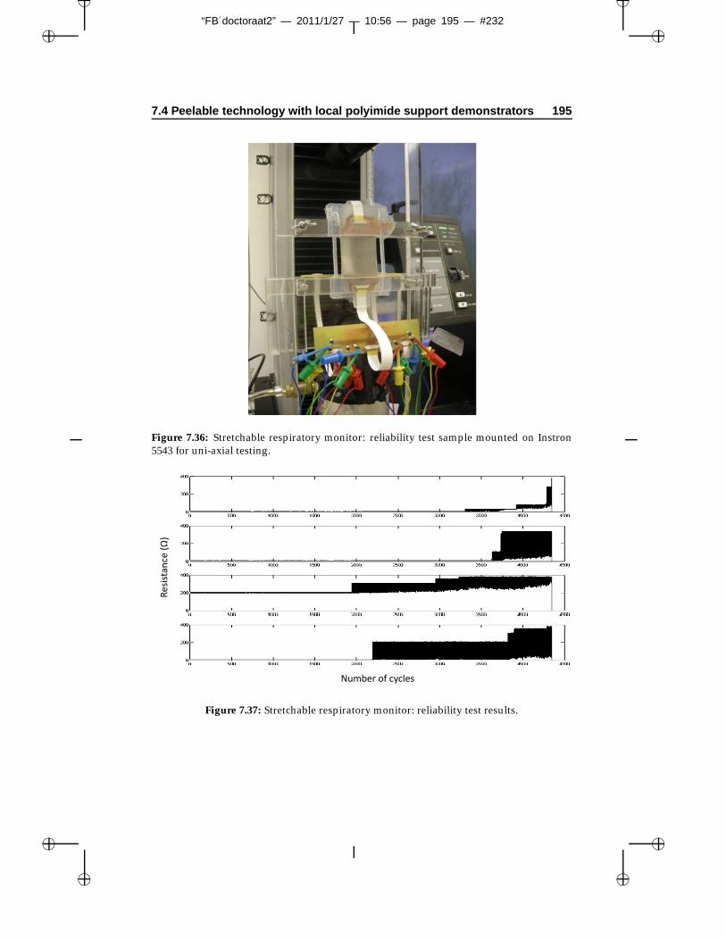
“FB˙doctoraat2” — 2011/1/27 — 10:56 — page 195 — #232�
�
�
�
�
�
�
�
7.4 Peelable technology with local polyimide support demonstrators 195
Figure 7.36: Stretchable respiratory monitor: reliability test sample mounted on Instron5543 for uni-axial testing.
e()
Resistance
Number of cycles
Figure 7.37: Stretchable respiratory monitor: reliability test results.

“FB˙doctoraat2” — 2011/1/27 — 10:56 — page 196 — #233�
�
�
�
�
�
�
�
196 Applications
7.4.2 Fitness activitiy monitor
Also within the frame of the European Stella project and in cooperation withPhilips, a fitness monitor has been developed. The device should be worn onthe body during fitness activities. For the demonstrator, its sensor-functions arefocused on energy consumption/weight management of the sportsman. For op-timal comfort, a compromise has to be made between size and stretchability: asmall, low-weight device enhances comfort but means that the substrate surfacearea is low, resulting in a low effective stretchable area.The demonstrator includes the following basic functions:
1. Sensor module with two sensors: acceleration (3D) and magnetic field (2D)
2. Processor (Coolflux from NXP)
3. Radio module for wireless data communication
4. Memory (Flash)
5. Power module
6. Power cell (battery)
The partitioning of the system over 5 interposer boards is shown in Figure 7.38and Figure 7.39.
Figure 7.38: Scheme of the Philips Fitness monitor.

“FB˙doctoraat2” — 2011/1/27 — 10:56 — page 197 — #234�
�
�
�
�
�
�
�
7.4 Peelable technology with local polyimide support demonstrators 197
Figure 7.39: Interposer boards used in the Philips Fitness monitor.
Movement sensors
The demonstrator is an example of a wireless body monitor, which is part ofa smart wearable system architecture. The wireless activity monitor transmitsrough 3-axial acceleration data, which are converted locally in e.g. accelerationgraphs or energy consumption. The sensors in the activity monitor are commer-cially available SMD sensors. As they are soldered on an interposer board, thesensor choice is not related to the stretchable technology. The acceleration is mea-sured in each of the three dimensions in a range of +/-2 g (optional +/- 6 g) andwith an accuracy of at least 2% (Kionix, KXM52-1050 [12]). The resolution is 1 mGwhich corresponds to a 13-14 bit data length. This accuracy should be reached formeasurements performed at a sampling frequency up to 1 - 1.5 kHz.The Magnetometer (Honeywell, HMC6052 [13]) has an accuracy of 5% in a range+/- 2 gauss and a resolution of 2 mgauss (11 bit). It is used to measure orientationrelated to the earth magnetic field.Due to the maximum substrate processing size of 10 cm by 10 cm, an adapted de-sign has been made to show the feasibility of the process by realizing this demon-strator. For the application, the demonstrator should have a straight design in thefinal version but due to the space restrictions, an U-shape design has been made,fitting on the substrate. The design with the different layers is shown in Figure7.40. It consists of the polyimide supporting layer, the copper and soldermasklayer. The feasibility of the process has first been tested by use of non-functionalinterposer boards, in order to check the connection between the interposers andthe stretchable substrate.

“FB˙doctoraat2” — 2011/1/27 — 10:56 — page 198 — #235�
�
�
�
�
�
�
�
198 Applications
Figure 7.40: Fitness activitiy monitor: polyimide mask, copper mask and solder mask.
Tests showed that the copper should be well cleaned before soldering. Pictures ofthe realization of the demonstrator are shown in Figure 7.41, Figure 7.42, Figure7.43 and Figure 7.45.
Figure 7.41: Production of fitness activitiy monitor: after polyimide definition, laminationand copper definition.
The functionality of the system has been demonstrated. Data was wirelesly re-ceived giving numbers about the 3 dimensional acceleration and the magneticfield observed. The device is still far from a commercial product but the functio-nality of the technology and the device has been succesfully demonstrated.

“FB˙doctoraat2” — 2011/1/27 — 10:56 — page 199 — #236�
�
�
�
�
�
�
�
7.4 Peelable technology with local polyimide support demonstrators 199
Figure 7.42: Production of fitness activitiy monitor: after soldermask definition.
Figure 7.43: Production of fitness activitiy monitor: after soldering test interposers (left)and functional boards (right).
Figure 7.44: Philips activitiy monitor: X-Ray measurement after vapour phase solderingfunctional boards. Voids in the solderballs can be observed.
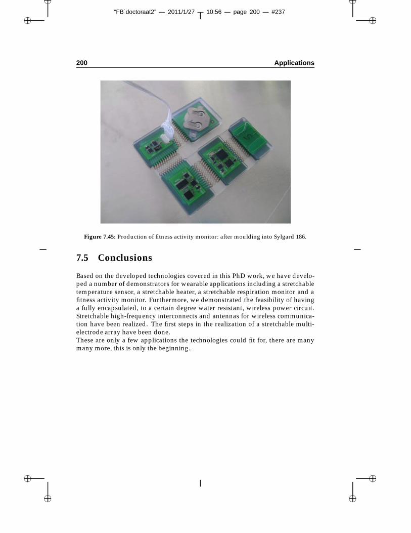
“FB˙doctoraat2” — 2011/1/27 — 10:56 — page 200 — #237�
�
�
�
�
�
�
�
200 Applications
Figure 7.45: Production of fitness activity monitor: after moulding into Sylgard 186.
7.5 Conclusions
Based on the developed technologies covered in this PhD work, we have develo-ped a number of demonstrators for wearable applications including a stretchabletemperature sensor, a stretchable heater, a stretchable respiration monitor and afitness activity monitor. Furthermore, we demonstrated the feasibility of havinga fully encapsulated, to a certain degree water resistant, wireless power circuit.Stretchable high-frequency interconnects and antennas for wireless communica-tion have been realized. The first steps in the realization of a stretchable multi-electrode array have been done.These are only a few applications the technologies could fit for, there are manymany more, this is only the beginning..

“FB˙doctoraat2” — 2011/1/27 — 10:56 — page 201 — #238�
�
�
�
�
�
�
�
References
[1] Y. Hsu, M. Gonzalez, F. Bossuyt, F. Axisa, J. Vanfleteren, I. De Wolf. In situobservations on deformation behavior and stretching-induced failure of finepitch stretchable interconnect. Journal of Materials Research, 24(12):3573–3582,DEC 2009.
[2] Y. Hsu, M. Gonzalez, F. Bossuyt, F. Axisa, J. Vanfleteren, B. Vandevelde, I.de Wolf. Design and analysis of a novel fine pitch and highly stretchableinterconnect. Microelectronics International, 27(1):33–38, 2010.
[3] Y. Hsu, M. Gonzalez, F. Bossuyt, F. Axisa, J. Vanfleteren, I. DeWolf. Theeffect of pitch on deformation behavior and the stretching-induced failureof a polymer-encapsulated stretchable circuit. Journal of Micromechanics andMicroengineering, 20(7), JUL 2010.
[4] I. Backers. Ontwerp en realisatie van een temperatuursensor in gea-vanceerde uitrekbare integratietechnologie. Master’s thesis, KatholiekeHogeschool Brugge-Oostende, 2005-2006.
[5] MICAS/ESAT KU LEUVEN. http://www.esat.kuleuven.be/micas/.
[6] B. Huyghe. Ontwerp en realisatie van rekbare flexibele hoogfrequent struc-turen voor personal health toepassingen. Master’s thesis, Ghent University,2006-2007.
[7] F. Axisa, F. Bossuyt, T. Vervust, J. Vanfleteren. Laser based fast prototypingmethodology of producing stretchable and conformable electronic systems.In 2008 2nd Electronics Systemintegration Technology Conference, number vol.2,pages 1387–90, 2008 2008.
[8] Dow Corning. Technical datasheet - Silastic MDX4-4210 Biomedical gradeelastomer with catalyst.
[9] T. De Prycker. Elastisch verwarmingselement met ingebouwd flexibel dis-play. Master’s thesis, Ghent University, 2006-2007.

“FB˙doctoraat2” — 2011/1/27 — 10:56 — page 202 — #239�
�
�
�
�
�
�
�
202 REFERENCES
[10] National Semiconductors. Technical datasheet - LM92 digital temperaturesensor.
[11] Dow Corning. Technical datasheet - Dow Corning 3-1818 Thermally Con-ductive Adhesive.
[12] Kionix. http://www.kionix.com.
[13] Honeywell. http://www.honeywell.com.

“FB˙doctoraat2” — 2011/1/27 — 10:56 — page 203 — #240�
�
�
�
�
�
�
�
Chapter 8
Conclusions and outlook
This chapter presents an overview of the main achievements within this PhD work and abrief look into the opportunities of future work.
8.1 Main achievements
The main objective of this PhD was the development of elastic microsystemstechnologies for large area applications for use in health care, functional clothesand for integrated electronics in stretchable parts and products. This includedthe development of a a new stretchable substrate with stretchable conductors,assembly technology adapted for stretchable substrates, integration methods forstretchable electronics in elastomeric parts and manufacturing methods for suchsystems. This based on the use of standard printed circuit board fabricationtechnologies, in order to make it as close as possible to conventional industryadapted processing techniques.
Different developed technology approaches have been presented, leading tothe most suitable technology approach described in Chapter 5. In order to makean electronic circuit stretchable, the system is subdivided in functional islandsconnected with each other through stretchable interconnections. The stretchableelectronic circuit is fabricated on a rigid carrier being attached to it by use of atemporary adhesive. Islands and interconnections are supported by a polyimidelayer, copper sheets are used to form the conductive traces and the fabricationmethod is close to standard PCB fabrication technology. After definition of thecircuit, pre-assembly and assembly steps including the mounting of electroniccomponents, the circuit is transferred into a stretchable polymer. This by meansof a 2-step injection moulding process by use of a dedicated mould.

“FB˙doctoraat2” — 2011/1/27 — 10:56 — page 204 — #241�
�
�
�
�
�
�
�
204 Conclusions and outlook
Reliability tests have been performed on the stretchable interconnects madeby different fabrication methods and stack buildups (polyimide support, sol-dermask covering,..). Also, the reliability of the interconnects to an embeddedinterposer has been tested.Pure copper, PDMS embedded meander tracks having a particular meander de-sign, can be stretched upto more than a million cycles for 0-2.5% elongation. Forhigher strains, 0-5%, 0-10% and 0-20% the average number of cycles is around17900, 2420 and 200 respectively. There is no increase of resistance during cyclicloading, a sudden breakdown is observed after a number of cycles. The effectof strainrate has been studied showing no significant difference between 1 and10% strainrate (s−1). The effect of having a soldermask layer on the interconnectshas been determined, resulting in a non significant improvement of the lifetime.Furthermore, polyimide as supporting layer showed a big increase in lifetime bya factor ~2-3.6 depending on the total applied strain. The supporting polyimideacts as a buffer between encapsulant and copper, and prevents crack propagationthrough the copper. For 0-5% strains, the lifetime increases upto ~90000.For all samples, the observed failure mechanism is fatigue due to accumulatedplastic strain at the top of the meanders. The accumulated strain in the copperleads to breakdown but can be prolonged by the use of the polyimide.A number of cyclic endurance tests have been performed on samples containingstretchable interconnects and a functional island, in order to study the behaviourat the rigid-flex-stretch transition. 2 types of samples have been made, a purecopper and a polyimide enhanced type of sample. The latter showed a lifetimeimprovement by a factor 3 for cyclic endurance tests for 0-10% elongation.
The development of the technologies has been supported by modeling activi-ties, in order to determine the effect of certain technology steps (addition ofpolyimide). Pre-knowledge has been used in order to make the first versions ofthe technologies. Modeling and analytical work has been performed on fabri-cated samples in the different technologies.
Several sidesteps have been investigated in order to improve or extend the tech-nology. This in order to increase the reliability performance and the functionalitythat can be implemented in the basic technology. The effect of adding polyimidehas been studied, below and above the conductors. The first steps in findingother ways to apply the supporting polyimide were explored. Screenprintingtests of non-photodefinable polyimide have been performed.We presented an extension of this technology by adding an extra conductor layer,screenprinted silverpaste, reducing the need of zero-ohm resistors in order torealize cross-overs and increasing the possible complexity of such a system.
A huge number of functional demonstrators have been presented, made in the

“FB˙doctoraat2” — 2011/1/27 — 10:56 — page 205 — #242�
�
�
�
�
�
�
�
8.2 Future work 205
various technologies: a stretchable temperature sensor, a wireless power circuit,stretchable waveguides, a stretchable heating element, a baby respiratory moni-tor, a fitness activity monitor,..
8.2 Future work
The technology, as presented in this PhD, had actually no special dedicated appli-cation in mind during its development; however in the meantime, many poten-tial applications have become apparent. Since its development, the technologymainly has been used for wearable electronics.In general one can say that applications for stretchable circuits are situated inthose areas where there is need for conformability (on or in the body):
• When the circuit is too large so that a single rigid or flexible componentisland is uncomfortable and thus the circuit has to be partitioned in smallerparts, interconnected by stretchable interconnects.
• When the desired functionality requires a large area with distributed com-ponents, which have to be electrically interconnected. Examples are largearea pressure sensor matrices e.g. for robotics or artificial skin, LED displaymatrices, the implementation of a distant electrode in an ECG monitor, etc.
The research presented, forms the base for a wide variety of further activities, try-ing to solve remaining problems or extending the technologies and applications:
• Work is going on for medical (up to implantable) and biomedical applica-tions. Therefore, a thin film version based on the same principles (circuitproduction before embedding) is being developed within the PhD of RikVerplancke. More dense circuitry, chip embedding and the use of more bio-compatible metals like Au, Pt are the main features of this technology.
• Application of the developed technologies to textiles, especially the washa-bility feature of the technologies and the combination with textile elementslike e.g. textile antennas and conductive yarns for interconnection is underinvestigation within different projects (BELSPO-SWEET project, FP7-Place-It project and FP7-PASTA project) and in the PhD of Thomas Vervust.
• Further improvement of the lifetime of the stretchable devices by optimiza-tion of the flex-stretch transitions, meander and island support technologyis planned. Reliability and washability of these stretchable circuits for dailyuse still needs to be proven.

“FB˙doctoraat2” — 2011/1/27 — 10:56 — page 206 — #243�
�
�
�
�
�
�
�
206 Conclusions and outlook
• Making certain process steps more cost effective and still more PCB fabcompatible (e.g. screenprinting of meander and functional island supportinstead of spinning and photopatterning).
However, the developed technologies have reached sufficient maturity so thattransfer to industry and real applications are under development:
• The developed processes are compatible with industrial PCB fabricationand assembly processes. Contacts with local industry for effectively verify-ing that certain process sequences can run in an industrial fab are ongoing.
• Evolution from small substrates until now (10 cm x 10 cm) to larger areaand replacement of lab type processing to fab type processes: planned pur-chase and installation of number of machines at CMST facilities capable ofhandling larger formats (9 inch by 12 inch, exactly a quarter of standardminimal PCB format).