notes of semiconductor technology, wafer fabrication and ... · notes of semiconductor technology,...
TRANSCRIPT

Notes of Semiconductor Technology, Wafer
Fabrication And Testing
June 2012
Abstract
Physics of Semiconductor materials, p-n junction, MOS transistors,Silicon technology (fabrication, or front End), packaging and assemply(back end),
1

Contents
1 Physics of Semiconductor Materials 31.1 Genesis . . . . . . . . . . . . . . . . . . . . . . . . . . . . . . . . 31.2 Band Model of Solids . . . . . . . . . . . . . . . . . . . . . . . . . 41.3 Crystal bonding model . . . . . . . . . . . . . . . . . . . . . . . . 131.4 P-N junction . . . . . . . . . . . . . . . . . . . . . . . . . . . . . 151.5 Transistor . . . . . . . . . . . . . . . . . . . . . . . . . . . . . . . 16
2 Silicon Technology (fabrication) 26
3 Testing and packaging 52
4 Conclusion 55
2

1 Physics of Semiconductor Materials
1.1 Genesis
At the basis of modern micro electronics, which is the basis on semiconduc-tors, devices there is Quantum Theory developed at the beginning of nineteenCentury.
In 1900, Planck came up with an equation that described the curve of radia-tion wavelengths at each temperature for a �black body radiation� 1. No matterwhat the material shape or shape of the container's wall, the results were thesame; the shape of the graphs depended only by temperature. Planck positedthat the surface of anything that was radiating heat and light � such the wallsin a black body device, contained �vibrating molecules� or �harmonic oscilla-tors�. These harmonic oscillators could absorb or emit energy only in the formof discrete packets or bundles. These packets or bundles of energy came onlyin �xed amounts, determined by Planck's constant, rather than being divisibleor having continuous range of values.This principle can be see again in the thephotoelectric experiment, which showed that the energy of the ejected electronswas proportional to the frequency of the illuminating light. This showed thatwhatever was knocking the electrons out had an energy proportional to lightfrequency. The remarkable fact that the ejection energy was independent of thetotal energy of illumination showed that the interaction must be like that of aparticle which gave all of its energy to the electron! This �t in well with Planck'shypothesis that light in the black body radiation experiment could exist only indiscrete bundles with energy. Photoelectric e�ect was known since the end ofeighteen century but Einstein was the one who given the correct interpretation,and by the way his studies of this e�ect was the reason for the Nobel price thegreat physician got in 1925. In another words we can see the photoelectric e�ectin this way: when we increase the frequency of the light the emitted electronssped out with much more energy. Then, when we increase the intensity of thelight by using carbon arc light that could be made brighter by a factor of 1000.The brighter, more intense light had a lot more energy, so it seems logical thatelectrons emitted would have more energy and speed away faster, But that didnot occur. More intense light produces more electrons, but the energy of eachremained the same. This was something that the wave theory of light did notexplain. Today we know that the behavior of the black body can be appliedalso at atomic scale range. Each electron of an atom can absorb or emit energyat speci�c frequency only at discrete values following the quite famous formula
E1 − E2 = hν (1.1)
where E1−E2 is the energy �jump� of the electron in the atomic model of Bohr
1A black body is an idealized physical body that absorbs all incident electromagneticradiation regardless of frequency or angle of incidence. It can be done with a small hole whenelectromagnetic radiation enters a cavity which walls re�ect inside and the radiation does notexit. From the �external world� is like if the external radiation has been completely absorbedby the hole, which represents the �black body�. A black body in thermal equilibrium (that is,a constant temperature) emits electromagnetic radiation called black-body radiation.
3

Figure 1.1: Black Body radiation
as �satellite� of the atom nucleus,ν is the frequency of the radiation, and h isthe Planck constant. When an electron absorb this packet of energy it emits anelementary particle called photon which exibits wave-particle duality (followsmaxwel's equations as well otpical rules!)
1.2 Band Model of Solids
Let consider electrons in an isolated atom. We know that an electron acted onby the Coulomb potential of an atomic nucleus may have only certain allowedenergies ( Figure 1.3 )
4

Figure 1.2: Bohr Atom and energy jump
Figure 1.3: Allowed energy levels of an electron acted on by the Coulomb po-tential of an atomic nucleus
5

In particular, by quantum mechanics theory, the electron can occupy one ofa series of energy levels below a reference energy taken as 0.
En =−Z2m0q
4
8ε2oh2n2
(1.2)
The electron carries charge −q so that q in 1.2 is a positive number. At lowtemperature, when more than one electron are associated with the atom, theelectrons �ll the allowed levels starting with the lowest energies. By the Pauliexclusion principle, at most two electrons (of opposite spins) may occupy a newenergy level.
Let us now consider the electron in the highest occupied energy level of anatom and neglect the lower �lled levels. When two isolated atoms are separatedby a large distance, the electron associated with each atom has the energyEn
given by 1.2. If two atoms approach one another, however, the full atomiccore of the �rst atom exerts a force on the second electron.The allowed energylevels for this electron are modi�ed due to this interaction (there is a change ofpotential).
An energy level En, can contain at most two electrons of opposite spin.When we approach the two atom for the same energy level En cannot cohabitfour electrons! When the two atoms are brought together to form one systemonly two electrons can be associated with the allowed energy level En. The twoother should go in a di�erent level quite close to En. In reality what happens isthat the allowed energy level En of the isolated atoms splits into two levels withslightly di�erent energies in order to retain space for a total of four electrons.
This principle is valid for all electrons of Atoms not only the last two in theenergy level En.As more atoms are added to form a crystalline structure, eachof the original quantized levels of the isolated atom is split many times. WhenN atoms are included in the system, the original energy level En splits into Ndi�erent allowed levels, forming the so called energy band which may containat most 2N electrons (because of spin degeneracy). Since the number of atomsin a crystal is generally large-of the order of 1022cm−3- and the total extent ofthe energy band is of the order of few electron volts, the separation between Ndi�erent energy levels within each band is much smaller than the thermal energypossessed by an electron at room temperature, and electron may easily jumpsbetween levels. Thus, we may speak of a continuous band of allowed energiescontaining space for 2N electrons. This allowed band is bounded by maximumand minimum energies, and may be separated by a so-called forbidden-energygaps, as showed in (Figure 1.4) or it may overlaps other bands. Electrons in oneband can easily jumps in the levels of this band, but their thermal energy atroom temperature does not allow them to jump the forbidden gap, so the namecomes from this constraints. The fact if these bands overlaps each other, or formsmall gaps or very large gaps determines the proprieties of a given material asconductor, semiconductor or insulator.
The allowed energy bands does not have the same depth. Electrons at highenergy levels (far from the central nucleus of the atom) are less tightly bound and
6
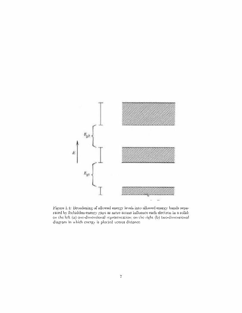
Figure 1.4: Broadening of allowed energy levels into allowed energy bands sepa-rated by forbidden-energy gaps as more atoms in�uence each electron in a solid;on the left (a) one-dimensional representation; on the right (b) two-dimensionaldiagram in which energy is plotted versus distance
7

Figure 1.5: Energy band diagram: N electrons �lling half of the 2N allowedstates, as might occur in a metal
may wander farther from the atomic core. If the electron is less tightly con�ned,it comes closer to the adjacent atoms and is more strongly in�uenced by them.This greater interaction causes a larger change in the energy levels and thisis re�ected in a wider energy bands for higher energy electrons of the isolatedatoms. We can see this in the Figure 1.4 where (a) is the one-dimensionalsketch. However often is useful to use a two-dimensional picture (b) wherethe vertical axis still represents the electron energy while the horizontal axisrepresents position of the electron in the crystal.
The formation of energy bands from discrete levels occurs whenever theatoms of any element are brought together to form a solid. So all solid innature will have this energy bands representation. We told that the distancesbetween these gaps cause di�erent electrical proprieties of solids. Let's take onemetal, the alkali. Each Alkali atom has a �free� valence electron in the outershell. Let's take a piece of Alkali of N atoms. As we discussed before all theseatoms when get closer to form the metal crystal structure split the allowedenergy levels of electrons from N (isolated atom) to 2N (all atoms together).The N valence atoms of the metal will occupy the �rst N energy levels but theycan easily jump by thermal energy at room temperature to one allowed level(N+1, N+2.... 2N). So when we apply a potential di�erence at the two sideof one metal, electrons excited with more energy can jump of some levels andcarries current. Metals solid are characterized by partially �lled energy bandand are hardly conductive (as in Figure 1.5).
In nature there are other materials which external valence atoms of theoutermost shell completely �ll the 2N energy band with 2N electrons and thereis an energy gap to the next band. In this case if the gap is su�cient high (withrespect the thermal energy of one electron which is some tenths of eV or less)the material has good characteristic of insulator (Figure 1.6). In an insulatoreven if we apply potential di�erence we do not see sensible current to �ow, atleast if we increase a lot the potential di�erence in order to provide quite a lot
8

Figure 1.6: Energy-band diagrams for an insulator. A completely empty bandseparated by an energy gap Eg from a band whose 2N states are completely�lled by 2N electrons.
9

Figure 1.7: Electron motion in an allowed band is analogous to �uid motion ina glass tube with sealed ends; the �uid can move in a half-�lled tube just aselectrons can move in a metal.
Figure 1.8: No �uid motion can occur in a completely �lled tube with sealedends.
of energy to some electrons who can �jump� the gap. In any case this does nothappens at room temperature. In good insulators the Eg is greater than 5 eV(in SiO2is 9 eV for instance).
We can do an analogy with horizontal glass tube with sealed ends whichrepresents the allowed energy states and the �uid inside representing the numberof electrons in a solid. In the case analogous to a metal, the tube is partially�lled (Figure 1.7). When a force (gravity in this case) is applied by tipping thetube, the �uid (= the current in the metal) can easily move along the tube. Inthe situation analogous to an insulator, the tube is completely �lled with �uid(Figure 1.8 ). When the �lled tube is tipped, the �uid cannot �ow since thereis no empty volume into which it can move; that is, there are no empty allowedstates!
semiconductors have band structures similar to insulators. The di�erencebetween these two classi�cations arises from the size of the forbidden energygap and the ability to populate a nearly empty band by adding conductivity-enhancing impurities to a semiconductor. In a semiconductor the energy gapseparating the highest band that is �lled at absolute zero temperature from thelowest empty band is typically in the order of 1 eV (silicon: 1.1 eV; germa-nium: 0.7 eV). In an impurity-free semiconductor the uppermost �lled band ispopulated by electrons which occupy all the allowed states, as before, but asthe energy gap Eg is not so big with respect the thermal energy of electrons, itcould happen that some electrons from the lower band �jumps� the forbidden
10

Figure 1.9: Energy-band diagram for a semiconductor showing the lower edgeof the conduction band (Ec) , a donor level (Ed) within the forbidden gap, theFermi level (Ef ), an acceptor level (Ea), and the top edge of the valence band(Ev)
energy gap and go in upper band. The uppermost �lled band is populated bythe electrons of the outermost shell, the valence electrons. For such a reasonthis band is called valence band. When an electron �jumps� the forbidden gapsgo in another band where it is completely free to move, and this cause possibilityto conduct some current. For such reason the upper band is called conductionband.
This structure is shown in Figure 1.9 . At any temperature above absolutezero (0° K = =273.15° Celsius), the valence band is not entirely �lled because asmall number of electrons possess enough thermal energy to be excited across theforbidden gap into the conductive band. Obviously the higher is the temperaturethe more are the electrons which jump the gap. Since only a small of electronsexists in this band (only the ones at the top level or the valence band), however,the current for a given �eld is considerably less than that in a metal. Thematerial behaves between a conductor and an insulator and for such a reason iscalled semi-conductor.
When electrons are excited from the valence band into the conduction band,left empty states in the valence band like a �bubble� in a liquid. If electric �eldis applied to the material the electron in conductive band move to the positive�eld causing current in the opposite direction and the �hole� left in the valenceband moves as well (in reality all others electrons moves little bit giving theimpression that is the holes which moves).
The concept of holes can be illustrated by our analogy with tube �lled with�uid. The semiconductor at absolute zero temperature appears as two sealed
11

Figure 1.10: Fluid analogy for a semiconductor. (a) and (b) No �ow can occurin the either the completely �lled or completely empty tube. (c) and (d) Fluidcan move in both tubes if some of it is transferred from the �lled tube to theempty one, leaving un�lled volume in the lower tube.
tubes one completely �lled, and the other completely empty (Figure 1.10(a)). When we apply a force by tipping the tubes, no motion can occurs (Figure1.10(b)). As said at higher temperature some electrons (the �uid) jumps thelevel. Is like if in our analogy some �uid is moved in the empty tube. The liquidin partially �lled tube moves as the tube is tipped and the �bubbles� left inthe almost completely �lled tube at the bottom due complementary movement.The liquid movement is the currents caused by electrical force (in our examplethe gravity).
Bubbles in the lower energy are called holes and exists only in the valencebands and only in relation to a conductive electron in the conductive band.
12

Figure 1.11: The diamond-crystal lattice characterized by four covalent bondedatoms. The lattice constant, denoted by λ is 0.543 for silicon and 0.356 fordiamond.
1.3 Crystal bonding model
The concept of holes and electrons in semiconductors can be also viewed in termsof the behavior of completed and broken electronic bonds in semiconductorcrystal.
We consider the diamond type crystal structure that is common in silicon(Figure 1.11). Each atom of silicon can create four covalent bond with fournearest neighbors by covalent bond with the external electrons, one from eachatom. The lattice structure is then repeated and this creates the crystal. Atabsolute zero temperature, all electrons are held in these bonds and thereforenone are free to move about the crystal in response to an applied electric �eld.In this state the semiconductors behaves as an insulator. As the temperaturebecome higher than absolute zero, thermal energy breaks some of the bond andcreates nearly free electrons which can then contribute to the current under thein�uence of an applied electric �eld.
After a bond is broken by thermal energy, the freed electron moves awayleaving an empty bond behind which can be replaced by another electron from anadjacent bond. The empty spaces behaves as a �bubble� which in semiconductortheory is called hole which moves in opposite direction with respect the electron.
13

Donors and Acceptors
In a pure semiconductor material the number of electrons n in the conductionband equals the number of holes p in the valence band. Such material is calledintrinsic semiconductor and the densities of electrons and holes in it (carrierscm−3) are usually sub-scripted i, as ni and pi. However, the most importantuses of semiconductors arise from the interaction of adjacent semiconductormaterials having di�ering densities of the two types of charge carriers (the p-njunction for instance).
As told intrinsic semiconductor is very bad conductor and in order to improvehis conductor characteristic we should �nd a way to improve the number ofcarriers (electrons in conduction band and holes in valence band). We can dothis by adding some �impurity� to the semiconductor crystal.
Let's take the example of the Silicon: his atoms have 4 covalent bonds withthe neighbors. If we introduce some small quantity of atom with 5 covalentbond (5 valence electrons), such as phosphorus, it create 4 covalent bond withone Silicon atom leaving the �fth electron practically free to move (only verysmall quantity of energy is necessary to move this valence electrons from thephosphorus core). Such atoms which provide one electron as additional freecarrier in the conduction band are called donors. In complementary way thereare atoms with three covalent bond which can �get� one electron from a Siliconatom and are called acceptors. In the �rst case the current is really caused bythe donated electrons. In the last situation the current is created by moving ofthe holes.
Without entering in details it is intuitive to understand that is more easyfor the �fth electron of the phosphorus to be �free� (i.e to jump into the con-ductive band) than for an electron of the Silicon. Physically this means that itrequires only a small energy to excite the electron from the donor atom into theconduction band, while a much greater amount of energy is required to excitean electron (of Silicon) from his valence band to the conduction band jumpingthe energy gap (even if we have seen that the energy gap for silicon is less thanthe energy gap of an insulator). Thermal energy at temperatures greater thanabout 150 K is generally su�cient to excite electrons from the donor atomsinto the conduction band. If we introduce impurity with 5 electrons in the lastenergy level, as we have seen we will inject electrons. The total number of thecarriers in the silicon atom �doped� with these impurity are
n+ ni + pi = n+ 2ni
Where n is the electron from the donors and ni = pi= intrinsic carrier. (Notethan n is � ni = pi).
In this case, we say we have created semiconductor of n-type where electronsn+ni are the majority carriers. A graph showing the conduction electron con-centration versus temperature for silicon and germanium is sketched in Figure1.12. Intrinsic holes density is equal to intrinsic electron density and we seehere than electron, for room temperature below 300 K till 600 K are fare morenumerous than holes in Silicon.
14

Figure 1.12: Electron concentration versus temperature for two doped semicon-ductors: (a) Silicon doped with 1.15×10¹⁶arsenic atoms cm−3, (b) Germaniumdoped with 7.5× 10¹⁵ arsenic atoms cm−3.
1.4 P-N junction
When we put close together semiconductor of p-type with a semiconductor ofn-type we creates the so-called p�n junction. This junction has the fundamentalpropriety to be able to allow current in one direction when a speci�c electric �eldis applied and show constant voltage drop. How it is possible is easy explained(Figure 1.13)
A p-doped semiconductor is relatively conductive thanks to majority carri-ers which are holes, positive charged, in the valence band. The same is true ofan n-doped semiconductor, relatively conductive by electrons which are major-
Figure 1.13: p-n junction
15

ity carriers in the conduction band. When we approach close together p-typesemiconductor with n-type semiconductor some electrons migrates from the n-type to the p-type semiconductors. When the electron's concentration at theboundary gap increase, an electrostatic voltage is creates which stop electronsmigrating from n-type to p-type semiconductors. The migrated electrons insidethe p-type semiconductors easily combines with the holes and creates a zone,exactly on the boundary where carrier density is almost zero. This zone is calleddepletion region as no carriers are present. The electrostatic voltage which hasbeen created due the electrons migrated from n-type to p-type semiconductorsprevent others electrons to move in that direction. But it is su�cient to applya negative voltage to the n-type semiconductor to push other electrons in thep-type semiconductors and to create a current �ow. For the speci�c structureof the system the voltage drop is almost constant (in the order of 0.7 volt) andcurrent quickly increase if voltage is increased.
On the other side, if opposite voltage is applied (positive to the n-type semi-conductor) this �depletes� again more the depletion region and prevent currentto �ow (if reverse voltage is not reaching a level called of breakdown which causehigh current to �ow).
We have so created a system which allows �ow current only in one directionand not in another. The p-n junction is the basis of semiconductor's deviceslike diodes which can be used to rectify alternate current for instance. In digitalelectronics p-n junction in forward-bias mode can be considered as closed-switch.
1.5 Transistor
If we add another layer of semiconductor we can creates the so-called n-p-n orp-n-p junction, which are the basic brick of transistor. A transistor is composedby one input, one output and a control gate. The control gate is the one where ifapplied appropriate voltage can make transistor working in di�erent zones. Thetransistor dependently how is powered (or polarized) can act as a signal ampli�eror a switch. When we apply sinusoidal signal to the input of a transistor whichhas been correctly polarized, the output signal is ampli�ed. We can see this asan analogy with a lever which can rotate in the vertical direction by a fulcrumpin which is not put in the middle. If we consider the transistor's output as thelever's motion at the end we can see this being ampli�ed (Figure 1.15).
Bipolar Junction Transistors (BJT) are used typically as ampli�ers in analogelectronics. For instance in Figure 1.16 is shown typical con�guration of onetransistor ampli�er common-emitter.
Digital electronics must manage digital signals. Digital signals are numberscodi�ed in binary code. So they are a series of 1 and 0. Physically number 1can be associated as the higher voltage level and 0 as zero voltage level at theoutput of an electronic system. In digital electronics so, all the signals are indiscrete form as series of ones and zeros. The most important component indigital electronics is the Metal-Oxide Semiconductor transistor (Figure 1.17).
Without entering into too many details we can see that main advantage ofMOS transistors with respect BJT are
16

Figure 1.14: charge density in the p-n junction boundary
17

Figure 1.15: Transistor as ampli�er in analogy with a lever rotating on a fulcrumpin
18

Figure 1.16: BJT as ampli�er
Figure 1.17: nMOS Transistor's layout
19

Figure 1.18: nMOS bias arrangement (a) and Drain current function of Drain-Source voltage when increasing the Gate-Source voltage
� Near∞ input resistance looking into gate vs. base current for BJT (betterbu�er on input side)
� Lower noise for high RS signal sources Better analog switch;
� truly ohmic at origin of VDS-ID plot (sample & hold)
� Compatible with digital CMOS (process cost advantage)
� Comes out of non-active operating region more quickly (BJT slow out ofsaturation)
� More robust current sources (gentler "crash" than BJT into saturation)
In order to simplify we can consider MOS transistor as �switched� which allowspassage of current or not dependently of the voltage applied in the gate. Whena speci�c voltage di�erence is applied to the gate (in a n-channel MOS mustbe positive) it is possible to create a n-channel just close to the gate junctionand so, when voltage is applied to the other two gate there is a current �ow.The input entrance of the current is called source, where the output is calleddrain. The current/voltage characteristic between drain and source can be seein Figure 1.18.
MOS as all transistors need to be bias with opportune bias circuit to thevoltage source (Figure 1.19)
Then in order to work as a digital switch in �closed� position (allowing cur-rent to �ow from Souce to Drain) it is necessary to create a speci�c �channel�between S and D. If we consider n-MOS transistor this is obtained by apply a
20

Figure 1.19: nMOS with bias circuit
positive voltage on the Gate (greater than a speci�c treshold voltage indicatedas V t). If the gate-source voltage is increased to a valueVGS > V t, an inver-sion layer is estabilished (you can imagine holes in the p-type layer immediatelyunder the gate are push out). This create the n-channel in n-MOS transis-tor (Picture 1.20). If there is voltage di�erence between Drain and Source thecurrent IDS can �ows. If VGS < V t this voltage is not su�cient to create aninversion layer, no channel exist and this cuto� the transistor. The MOS asdigital switch is �open� (no current �ow)2
With n-MOS transistor is very easy to fabricate the basic bricks to do digitaloperation. As we have told microcomputers understand only number as seriesof low voltage- high voltage status (zeros and ones).This universe with one digitnumber is called Boolean algebra, and Boolean operation can be de�ned. Thebasic one is the INVERTER. It is easy with MOS transistor to make a circuitwhich execute such operation (Figure 1.21 ) . Another fundamental operationin the Boolean algebra is the NAND which can be shown in Figure 1.22 .
We will see in the next chapter the basic manufacture steps from a singlecrystal silicon wafer to make MOS transistors. In order to be able to make all thealgebraic operation in Boolean algebra is necessary to use two di�erent of MOS,p-type and n-type. So the fabrication process will make on the same single-crystal silicon wafers a lot of transistors of n-type and p-type close together,what we call Complementary MOS systems (Figure 1.23 ).
2Actually there is always a leakage current between Dranin and Source but at this stagecan be ignored.
21

Figure 1.20: Channel creation in n-MOS transistor.
Figure 1.21: nMOS as inverter (NOT)
22

Figure 1.22: nMOS as NAND circuit
23

Figure 1.23: Cross section of CMOS inverter in n-well process
24

Semiconductor's companies like NXP are specialized in the manufacturing ofa lot of transistors in the same single crystal wafer. But, how many transistors?It is quite known now the famous �Moore's Law� :Moore's law is a rule of thumbin the history of computing hardware whereby the number of transistors that canbe placed inexpensively on an integrated circuit doubles approximately everytwo years. The period often quoted as "18 months" is due to Intel executiveDavid House, who predicted that period for a doubling in chip performance(being a combination of the e�ect of more transistors and their being faster),Figure 1.24.
Figure 1.24: Moore's law
This means that technology improvement give the possibility to put on asame single-crystal wafers, more and more transistors. Technology limit is de-�ned by the smallest part of CMOS transistor which litographic and chemicaletching processes described in the next chapter. Most critical part to build arethe holes for metal connection, metal deposition and channel's lenght. Todaystate of the art technology in smart card semiconductor's market reached arange between 40 and 90 nanometers (1nm = 10−9m).
We will see in the next chapter the basic fabrication's steps to make billionsof MOS transistors on a silicon wafers of some inches.
25

2 Silicon Technology (fabrication)
Silicon C-MOS fabrication steps and Masks fabrication stages. All begun withthe growth of the pure Silicon crystals. Silicon is the common element foundedin sand. 28% of Earth Crust, second only to Oxygen! The silicon from sand isre�ned and puri�ed as poly silicon chunks . The �puri�ed� silicon is then heatedto a �molten� state. A small solid pieces of single crystal of Silicon called �seed�is gently loaded in a rotate vap (quartz crucible) of molten silicon (Figure 2.1 ).
Figure 2.1: From poly-silicon to single crystal silicon
Using the cubic atomic structure of the seed a new crystal is created as thesymmetrical extension of the seed (Figure 2.2
The hot liquid silicon in contact with the seed becomes cool and solidi�esand is gently raised from the molten region. As it is raised it cools, and materialfrom the melt adheres to it, thereby forming a larger crystal. Under the carefullycontrolled conditions maintained during growth, the new silicon atoms continuethe crystal structure of the already solidi�ed material. The desired crystal diam-eter is obtained by controlling the �pull rate� and temperature with automaticfeedback mechanism. In this manner cylindrical �single-crystal' ingots of Siliconcan be manufactured (Figure 2.3)
The cubic atomic structure of silicon consists of atoms with four electronsin the outer electron orbit (covalent bond) Figure 2.4, and Figure 2.5
In a perfect crystal and in a low temperature each silicon atom bonds withis neighbors, there are no free electrons to conduct currents.
At room temperature however, the silicon crystal has enough small thermalenergy to �free� a small number of electrons (electrons that bypass the forbidden
26

Figure 2.2: Cubic Atomic Structure
Figure 2.3: Single crystal silicon coming from furnace
27

Figure 2.4: Silicon Atomic Structure
Figure 2.5: Silicon four covalent bond
28
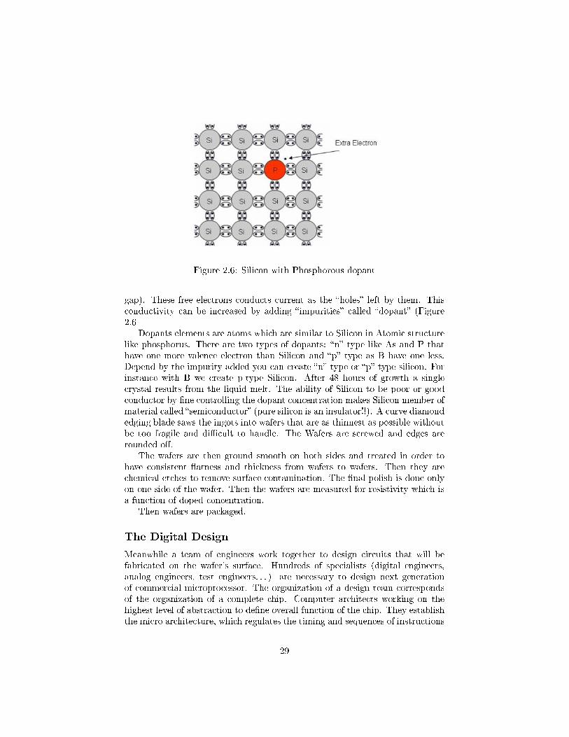
Figure 2.6: Silicon with Phosphorous dopant
gap). These free electrons conducts current as the �holes� left by them. Thisconductivity can be increased by adding �impurities� called �dopant� (Figure2.6
Dopants elements are atoms which are similar to Silicon in Atomic structurelike phosphorus. There are two types of dopants: �n� type like As and P thathave one more valence electron than Silicon and �p� type as B have one less.Depend by the impurity added you can create �n� type or �p� type silicon. Forinstance with B we create p-type Silicon. After 48 hours of growth a singlecrystal results from the liquid melt. The ability of Silicon to be poor or goodconductor by �ne controlling the dopant concentration makes Silicon member ofmaterial called �semiconductor� (pure silicon is an insulator!!). A curve diamondedging blade saws the ingots into wafers that are as thinnest as possible withoutbe too fragile and di�cult to handle. The Wafers are screwed and edges arerounded o�.
The wafers are then ground smooth on both sides and treated in order tohave consistent �atness and thickness from wafers to wafers. Then they arechemical etches to remove surface contamination. The �nal polish is done onlyon one side of the wafer. Then the wafers are measured for resistivity which isa function of doped concentration.
Then wafers are packaged.
The Digital Design
Meanwhile a team of engineers work together to design circuits that will befabricated on the wafer's surface. Hundreds of specialists (digital engineers,analog engineers, test engineers. . . ) are necessary to design next generationof commercial microprocessor. The organization of a design team correspondsof the organization of a complete chip. Computer architects working on thehighest level of abstraction to de�ne overall function of the chip. They establishthe micro architecture, which regulates the timing and sequences of instructions
29

Figure 2.7: Wafer Screwed
Figure 2.8: Wafer Rounded
30

Figure 2.9: Wafer resistivity measurement
that tell the microprocessor what it has to do. The design is divided in areathat performs speci�c functions. Each unit is assigned to a designer that worksat �logic leve3to create detailed speci�cations and establish hardware needs.Each unit is sub divided into functional blocks. Each block is assigned to acircuit designer who works at �transistor's level� . The circuit design consiststo connect transistors in speci�c way. At digital level the transistor works likea �controlled switch�. It can switch hundreds of millions time in a second.The number of switching in a de�ned period de�nes the operation frequencyof the unit. Electrical information is digitized in �0� and �1� that correspondsto the �machine language� understandable by the next abstraction layer of thedigital system. How a transistor works? The most commonly used transistor inthe digital world is the Complementary Metal oxide Semiconductor Transistor(CMOS, Figure 2.10
The n-channel transistor has two heavily n-type doped silicon region, sepa-rated by an electron's poor �p� type substrate. The edge region called �SOURCE�and �DRAIN� becomes ends of electronic switch that is normally o�. The �gate�electrode is close too, but electrically insulated by the p-type region. The ap-plication of small positive voltage create a small positive charge on the gate.This charge attracts the electrons from the drain to source region turning theswitch on. When the gate voltage return to zero the transistor is again OFF.
3di�erent abstraction level can be de�ned depending what we de�nes as the basic design�brick�. At physical level we consider the basic elemend the Atom. At analog level the basicbrick is the MOS transistor. At digital level it is the NAND or equivalent gate which is agroup of MOS transistors.
31

Figure 2.10: CMOS layout
The p-channel works in the same way with inverted current carriers. It is pos-sible to fabricate p-channel and n-channel transistors on the same wafers bydoping section of the wafers (note that the doped zone I some micrometers withrespect the total thickness of the wafer which can be hundreds or nowadays tensof micrometers) This technology is known as Complementary MOS transistorbecause a gate voltage which turns a p-channel transistor on, turns an n-channeltransistor o�. Design requires SW and HW tools called Computer Aided Designand Computer Aided Engineering.
After circuits designers completes each block of circuitry, the computerchecks for accuracy based on geometrical and electrical design rules (Figure2.11)
Masking
A �MASK� designer (the layout step of the design) takes the circuit's schematicsand manually lay out the channel in each level of the mask and generate somemaster blueprint. These drawing are using four or �ve hundreds time the actualsize of the chip and enable engineers to visually check for errors. This informa-tion is then electronically fed into beam machine. In an ultra clean environmenta electron's beam will �nal etches the patterns and does a series of crowns platesand glass plates. After the glass plates are etched they becomes the so-called �MASKS� that are used to transfer the circuit patterns into wafers. Each maskis inspected to assure the masks are good. The masks go in a �nal wash in acidbefore they are carefully packaged. The �rst mask create a wall doping so thatneighbor n-type and p-type substrates exists on the same wafer. The p and n
32

Figure 2.11: CAD layout of front end digital design
channel regions are speci�ed and electrically isolated by the growth of siliconDioxide SiO2
SiO2 is an insulator which creates on the surface of the silicon exposed tothe air (oxidation).
Next the gate electrodes which turn the transistor ON and OFF are formed.Masks number four and �ve de�ne the SOURCE and the DRAIN regions
of the n-channel and p-channel transistors. The next masks de�nes the contactholes which will enable the aluminum wires used to interconnect the individualtransistor to contact the source , the gate and the drain region of each transistor.
Most of integrated circuits use several numbers of masks (between 30 and40 in the current CMOS90 technology for smart cards) depending on the com-plexity of the circuit and the type of process4. From start to �nish a completeprocess may involve hundreds of individual operations and may take severalweeks to complete. To handle successfully silicon runs, controlled contamina-tion is extremely important. It takes just few microscopic particles in the airto drastically impact the level of impurity allowed and �nally to drastically re-duce the �nal �yield� of a semiconductor wafer. Yield of semiconductor wafer isthe ration between the number of total �working� chip (= circuits designed =interconnection of transistors) into a wafer divided by the �non working chip�(this will be discussed later during the test). The gas and chemical substancesthat come in contact with silicon wafers must also be of highest purity and freeof contamination. To start C-Mos fabrication p-type wafers with a speci�c re-sistance are selected. All type of IC including C-MOS is fabricated using four
4there are di�erent type of MOS which can be created. High power MOS for power supplyapplications. Floating gates for non volatile memories. Extremely high frequency frequenciesMOS for other applications. . . each steps introduce a new mask in the design!
33

Figure 2.12: Mask insertion
Figure 2.13: Di�usion impurity
34

Figure 2.14: Silicon Dioxide as insulator layer
Figure 2.15: Gate's electrode poly-silicon's maided
35

Figure 2.16: Metal interconnection
36

basic techniques (in sequence)
1. Formation of thin layers of silicon dioxide
2. Introduction of dopants atoms
3. Deposition of a variety of insulating and conductive (metal) materials
4. Precision pattering of each of these layers
Before the process begins the laser scribed identi�cation number of each waferis recorded. We start by cleaning the p type of the wafer in hot acids. HCl,ammonium hydroxide are necessary to remove all the organic and metal's con-taminants. This cleaning procedure is repeated sometimes to make sure thesurfaces of the wafers stay absolutely clean. The wafers are then put into DE-ionized water and dry in spun dried in �ltered nitrogen gas. In a vertical furnacehigh temperatures will be used to growth layers of silicon dioxide. SiO2 is glass-like insulator which protects the silicon's substrate. Pure oxygen reacts with thesilicon surface in hot furnace, to growth on a thin layer of silicon dioxide. Thisis similar to the oxidation of the car paint which is brilliant at the beginningand become dark at the end for the oxide formation. In the car's paint theoxide formation is a process which allows also protecting metal in case paint ispartially removed. The silicon dioxide layer will be etched with a stencil andcreates some windows where to dope speci�c region of the wafer. But �rst thepattern of the stencil is applied to the silicon dioxide through a photographictechnique called photo-lithography.
Photo-lithography and etching
The �rst mask pattern will be transferred into the wafer using photo resist, amaterial which is sensitive (i.e can be removed by) light. The wafer is transferredin heating plates and baked low temperature to evaporate the solvent living athin layer of photo resist. The wafer then enters in a computer controlledmachine called STEPPER. Inside the wafer is positioned under selected mask'spatterns. There are two type of photo resist: negative and positive. A negativephoto resist hardens when exposed to light and remain on the wafer when thewafer is developed under light. A positive photo-resist when exposed to UVlight is removed on the other side. The region of silicon dioxide unprotected byphoto-resist is then etched (Figure 2.17 ).
Acid dissolve silicon dioxide but as it can dissolve in all direction can createsunder cutting that cause inexact transfer of the mask (Figure 2.18 )
37

Figure 2.17: Etching
Figure 2.18: Acid dissolution
When critical �ne etching is needed wafer goes through a DRY etching pro-cess called PLASMA etching.
In a PLASMA chamber a chemical reactive gas provides the �uorine atomswhich react with exposed silicon dioxide to leave short vertical walls. Highlymagni�cation of microscope photograph shows precision of this etches regions(Figure 2.19 )
The harden resist is then removed in a dry process by using oxygen plasmawhich may include �uorine followed by hot acid baths. This leaves the silicondioxide layer as insulator (for insulation purposes). Photo-lithography will beused by each and subsequent masks of the process.
Figure 2.19: dry etching
38

Figure 2.20: Mask one
Patterning
We are then at the last stage: precision patterning of each of these layers. Thistechnique allows insulating microscopic region of the wafers and constructingcomponents of the electronic circuit. In this way the transistors and the circuitsare gradually built a layer at time. Doped ions will bombard the wafers to createn-type regions. The depth of the ions implantation depends on the amount ofenergy used. Doped ions are separated by other elements and accelerated inhigh speed in a strong electric �eld. The ions are then driven into the waferimplanting exposed silicon's regions (mask 1, Figure 2.20) . The silicon dioxidelayer blocks the dopants for unwanted regions.
Because in our examples these wafers are p-types, phosphors' ions which aren-type dopant are implanted. Exposing the wafer to higher temperature di�usethe n-ions into deeper in the Silicon substrate (Figure 2.21 ).
This create the wall of n-type substrate where the p-channel (well) transistorswill be build. In the wafer where n-type boron has been implanted to createp-wells regions to create n-type transistors.
39

Figure 2.21: di�usion of n-ions into deeper in the Silicon substrate
Deposition of Variety of Insulator and conductive materials
In a deposition furnace a layer of Silicon nitrate is deposited over the oxidelayer. This prevents the additional growth of the silicon dioxide and protectsthe region when the transistors will be built.
Photo resist again is evenly spread over the wafer and baked in preparationfor the next mask. Using a computer aided machine each new mask is perfectlyaligned on the pattern over the wafer. The second mask used to de�ne the actualtransistor's region is also exposed across the surface of the wafer. The waferagain is developed to remove the second photo resist and baked and plasmaetched. The free �uorine atoms react with the exposed nitrate (the insulatorcreated in the previous step). After the photo resist is removed the wafer goesback into the oxidation furnace for the growth of new silicon dioxide layer. Athick insulator layer of silicon dioxide known as Field Oxide (FOX) will be grownwhen the nitrate has been etched. To growth this thick layer of Oxide, Oxygencombined with hydrogen is introduced into a wafer as steam. This insulationreduces the electric �eld between the surfaces and the underlines regions (Figure2.23)
This region through the microscope FOX looks like white boundaries. Itwill avoid current leaking between devices allowing thousands of transistors tocoexist in the small area (Figure 2.24)
The remaining nitrate layer is then removed by a combination of dry andwet chemical etching. The wafers are then implanted with Boron's ions whichpenetrate the Silicon substrate and through the thin Oxide layer (FOX).
40

Figure 2.22: Deposition of Silicon nitrate
Figure 2.23: thick insulator layer of silicon dioxide known as Field Oxide (FOX)
41

Figure 2.24: FOX microscope
Figure 2.25: Boron's ion implantation
42

Figure 2.26: Gate electrode
This will provide the uniform electrical characteristic in the region when thetransistor will be built. The FOX is removed and new Silicon Dioxide is grown inthe gate area. In the vertical furnace the gate electrode will be formed with thep poly-silicon which will consist in many small grain of electrically pure silicondoped with p to make more conductive. With photo-lithography p poly-siliconis then etched to create gate of poly which will turn transistors ON and OFF(Figure 2.26)
The poly Silicon is dry etched to carefully control this gate's fabricationprocess. The depth of this gate de�nes the distance which separates the Drainby the Sources and ultimately the speed of the circuit and the technology size.The gate becomes the �rst conducting layers connecting di�erent transistors.
After Mask 4...
Mask number 4 allows implantation of n-channel regions highly concentratedof n type dopant (n+) to form the highly conductive source and drain regionsof the n-channel transistor. Mask number 5 will create p+ regions of p-typetransistors. Photo resist is removed and again wafers are cleaned.(Figure 2.27)
The wafers are put in a furnace and wafer's defects created by ION implan-tation are repaired. Next a thick insulator glass layer is deposited. All previouslayers are covered with this depth glass layer. Surface then must be planarized
43

Figure 2.27: Creation of p+region
to ensure that every part of subsequent mask layers are transferred in sharpfocus. Planarization is done by chemical / mechanical methods which is usedto polish out a tick surface layer on the wafer's surface./ This creates the �atsurface for high resolution patterns (Figure 2.28)
The Mask number 6: Always by photo lithography will be de�ned the open-ing holes where the metal wiring will be used to interconnect (in the way de�nedby the circuit design) the source, the drain and the gate of each transistor. Con-tact holes are created on silicon dioxide by plasma etching (Figure 2.29).
Through the microscope these holes are seen as small dots (Figure 2.30)
Metal layer
Metal will be �lled in holes to ensure solid and good electrical connection. Tung-sten metal layer is deposited over the surface to complete the �ll of tiny holes.Then metal is etched and polished. Now source and drain of each transistor areconnected with this metal (Figure 2.31)
A layer of aluminum silicon alloy is deposited on the surface to become the�rst level of circuit wiring (Figure 2.32)
44

Figure 2.28: Opening holes for metal interconnection
Figure 2.29: Mask 6
45

Figure 2.30: Metal holes showed as small dots through the microscope
Figure 2.31: Injection of tungsten meta
46

Figure 2.32: Deposition of aluminum layer
Mask number 7 patterns the aluminum. This is the �rst level in which thesingle transistors are connected together to form complex blocks of circuitry.
The aluminum alloy is removed by using dry etching and photo resist isremoved (Figure 2.34)
It is impossible with only one layer of aluminum to connect transistors inall the complicated way required by the circuit design. Several subsequentadditional level of aluminum wiring are often produced on the same circuit. Forinstance in the picture 2.35 (Scan Electronic Microscope photograph) it can beseen the connection with two metal layer.
The picture 2.36 show cross section of 5 metal layers.
Each next metal layer typical requires TWO additional masks and the fol-lowing process step: 1. Deposition of Silicon Dioxide (to electrically insulate onthe subsequent metal wiring level) 2. Photo-lithography masking and etching
47

Figure 2.33:
to open the contact holes between the top metal layers and next layer to be de-posited 3. Deposition in the contact holes of another tungsten plug: this insurea good electrical connection between wiring levels and more planar surfaces 4.Deposition and patterning of the new upper level of aluminum alloy
Pads
After all the desired level of metals interconnects are in place, a �nal level ofsilicon nitrate is deposited to protect the fragile aluminum alloy connect. In the�nal photo-lithography step only the nitrate on the top bonding plates is etchedaway. Aluminum pads are the places where contacts from/to the external linesto/from chip are done. The wafers are then stripped of photo resist and the runis complete! 9Figure 2.37)
Go to Test
Finally the wafers are ready for electrically testing and packaging. If the digi-tal design corresponds to embedded micro-controllers with ready only memory(ROM) which contains hardwired microprogammed code, this is done during thevery last �metal masks� of the silicon runs. Wafers with non programmed ROMare called �partially di�used� and when ROM is microprogrammed (masked)wafer is fully di�used. Typically the ROM contains programs which does not
48
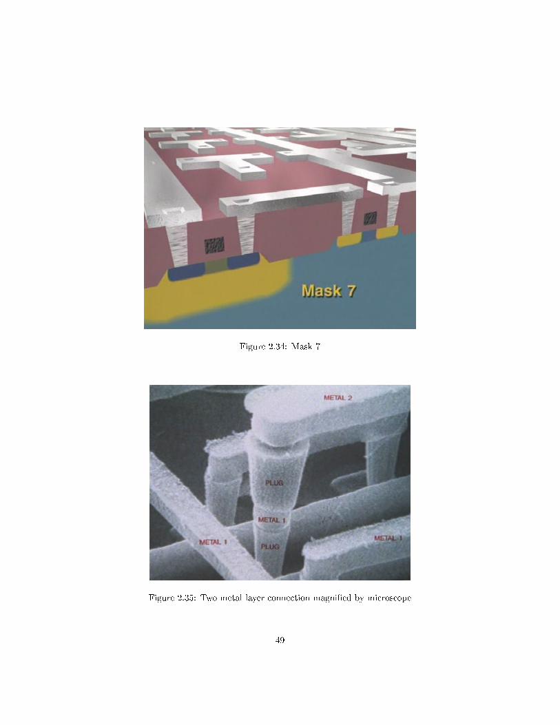
Figure 2.34: Mask 7
Figure 2.35: Two metal layer connection magni�ed by microscope
49

Figure 2.36: Cross section of �ve metal layers
Figure 2.37: PAD magni�cation
50

need to be changed once the chip is designed (low level routines for the behaviorof the micro controllers, operating system etc. . . ).
51

3 Testing and packaging
In testing the wafer slides are put in probes machines, where thin metal probesmakes contact with thin metal pads of circuitry for testing the �ow of electricalcurrent (�gure 3.1) A computer keeps tracks of which circuit has failed. Aspecial machine �ink dot� or marks the failed circuits (Figure 3.2) (today thisis done by an electronic ink process where the ink-dot map is recorded on amagnetic or optical disc provided with the wafer). Each chip did not pass thetest is marked.
Figure 3.1: chip testing
Then wafers are mounted in a sticky tape to keep them intact as the indi-vidual circuits are separated (Fig. 3.3)
An optical scanner aligns wafers by speci�c points. Then in soap waterdiamond sock cuts the silicon wafer without cutting the tape: this is the processto create the so-called `swan wafers�. Today the cut can be done via lasertechniques (�laser sawing�).
Then each dice is picked and placed in container which constitutes the �pack-age�. The dice's pads should be connected with the package's I/O pins. Thisprocess is done with a process called �wire bonding�: thin gold wires are usedto electrically connect the dies to the so called LEAD FRAME (Fig.3.4 )
This pins or lead �ngers of the frames are now attached to the microscopiccircuitry of the integrated circuitry to protect the circuit and its fragile wirebonds. The devices can be �nally encapsulated in hard plastic (the package).This requires two sided mold. Between each operation the bottom mold is
52

Figure 3.2: Wafer ink-dotting
Figure 3.3: Sawn wafers mounted on sticky tape (Film Frame Carrier)
53

Figure 3.4: Wire Bonding
brushed and cleaned. The cylinder cavities will be hold pieces of plastic ma-terials when heated the melted plastic will �ow to small channels and �ll therectangular cavity which will hold the device. After several minutes the encapsu-lation process is completed. The remaining plastics are removed from the mold.The leads are now prepared for plating. Inside one machine under high pressuresands and impurities dusts are blasted away. In ovens the plastic molten is fullycured. In the plating process the strips are loaded on carriers and depth in aseries of chemical and water's washed baths.
Packaged chip can then pick and placed on printed circuit boards (PCB)where special cavities are created where to �x the chip (the socket). Individualchips are removed from strips, the lead cut from the frames and bent into the�nal con�guration.
Before be mounted the chip must to be tested, they are in this case loadedin to a burning boards which will be placed into ovens. These boards consist inmany electrical circuits which allow electrical contact with circuits to stress thechip in several con�guration and under several mechanical and temperaturesconstraints. The number of the input/output pins of a chip is normally quitebigger in this con�guration (where the Device is Under Test) with respect the�nal phase where the chip is put in productions: a lot of pins are created just fortest purpose and will be cut out in production (this also for security reasons).In these boards the chips are stressed far beyond their normal conditions. Eachchip is forced to fail prematurely. This stress which can continue for severalhours encourage potential defects to occur faster. Other tests expose chip to
54

extremely temperature changing conditions. All these tests are used to de�nethe Product Characterization (a series of electrical measures done on the chipunder several temperatures and environmental condition) which make possibleto check if the chip works under the speci�ed range of the design (typically theserange are indicated in the last part of the chip data-sheet). After this test thechip are packaged for �nal shipment.
4 Conclusion
To terminate this quick overview on VLSI manufacturing process, let's considera very simple visual analogy to summarize the wafer fabrication and the dif-ferent masking processes. If we consider �our as the equivalent of rough sand,this is the initial step for the fabrication of a single crystal semiconductor wafer(Figure 4.1). Polycrystalline silicon (poly-silicon or brie�y poly) is puri�ed sili-con extracted from sand, but still composed of many small crystals with randomorientation. This mix of purity and disorder can be represented by �our! (Fig-ure 4.2). The process to fabricate a single crystal silicon ingot is due to somephysical and chemical reaction which happens inside the furnace. We can makean analogy with the process rising of the �our with water; in actual fact in our�pizza-making� analogy the growth is generated by forces inside the mixturewhereas in the growth of single crystal silicon is mechanical pull by an externalforce (Figure 4.3). Once created the single crystal silicon ingot (in our examplethe raised pasta) a single crystal wafer is created. In our example this can berepresented by a single layer of �pasta� which is the common element for eachpizza (Figure 4.4).
Di�usion 1 is the creation of the circuits for a speci�c design. If we are designa micro-controller this means the di�usion 1 will de�ne the micro-controllersblocks and interconnection but we still do not de�ne eventually any content forthe �nal ROM (the metal layer). We can consider this process quite generic. Inour �pizza� world di�usion 1 is when we put a �rst layer of tomato on the pizza(we can argue not all pizza are tomato maiden, of course! As not all waferscontains microprocessors!): Figure 4.5. Finally (Figure 4.6) the di�usion 2 isthe �customization� of the product which de�ne the very last metal layers. Inthis case we decided to customize the pizza-wafer like a �margherita�. Beforeshipping the circuits it should be tested (Figure4.7) and eventually sawn (Figure4.8) (it is not mandatory as this can be a stage for a sub contractor), and �nallythe products are shipped to the next fabrication step, very likely the assembly(Figure 4.9)
And hopefully on time!
55

Figure 4.1: The sand like wheat
Figure 4.2: �poly silicon�
Figure 4.3: Single-Crystal Growth
56

Figure 4.4: Single-Crystal wafer
Figure 4.5: Di�usion-1
Figure 4.6: Di�usion-2
57

Figure 4.7: Test!
Figure 4.8: Sawing
Figure 4.9: Transport to assembly
58

References
[1] John P. Uyemura, Fundamentals of MOS Digital Integrated Circuits:Addison-Wesley, 1988
[2] Richard S. Muller, Theodore I. Kamis, Device electronics for integrated cir-cuits, 2nd edition: John Wiley & Sons, 1986
[3] J. Milman, A. Grabel, Microelettronica, McGraw-Hill, 1994
[4] Walter Isaacson, Einstein his life and universe, Simon & Schuster, 2007
[5] Giuseppe Montuschi, Imparare l'elettronica partendo da zero, Nuova Elet-tronica, 2000
[6] Ruth Carranza, Silicon Run I/II, 1996, http://www.siliconrun.com
59