nonideal op amp
TRANSCRIPT
EE 312 Electronics II
LECTURE NOTES:
Nonideal Characteristics
1 | P a g e
© 2013 King Abdulaziz University Dr. Amjad Hajjar Electrical & Computer Engineering Department
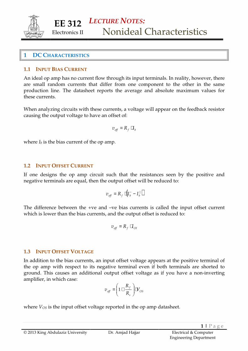
1 DC CHARACTERISTICS
1.1 INPUT BIAS CURRENT
An ideal op amp has no current flow through its input terminals. In reality, however, there are small random currents that differ from one component to the other in the same production line. The datasheet reports the average and absolute maximum values for these currents. When analyzing circuits with these currents, a voltage will appear on the feedback resistor causing the output voltage to have an offset of:
bfoff IRv ⋅=
where Ib is the bias current of the op amp.
1.2 INPUT OFFSET CURRENT
If one designs the op amp circuit such that the resistances seen by the positive and negative terminals are equal, then the output offset will be reduced to:
( )+− −⋅= bbfoff IIRv
The difference between the +ve and –ve bias currents is called the input offset current which is lower than the bias currents, and the output offset is reduced to:
OIfoff IRv ⋅=
1.3 INPUT OFFSET VOLTAGE
In addition to the bias currents, an input offset voltage appears at the positive terminal of the op amp with respect to its negative terminal even if both terminals are shorted to ground. This causes an additional output offset voltage as if you have a non-inverting amplifier, in which case:
OS
s
f
off VR
Rv ⋅
+= 1
where VOS is the input offset voltage reported in the op amp datasheet.
EE 312 Electronics II
LECTURE NOTES:
Nonideal Characteristics
2 | P a g e
© 2013 King Abdulaziz University Dr. Amjad Hajjar Electrical & Computer Engineering Department
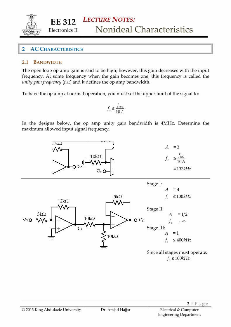
2 AC CHARACTERISTICS
2.1 BANDWIDTH
The open loop op amp gain is said to be high; however, this gain decreases with the input frequency. At some frequency when the gain becomes one, this frequency is called the unity gain frequency (fUG) and it defines the op amp bandwidth. To have the op amp at normal operation, you must set the upper limit of the signal to:
A
ff UG
s 10≤
In the designs below, the op amp unity gain bandwidth is 4MHz. Determine the maximum allowed input signal frequency.
kHz
A
ff
A
UGs
133
10
3
=
≤
=
Stage I:
kHzf
A
s 100
4
≤=
Stage II:
∞→=
sf
A 21
Stage III:
kHzf
A
s 400
1
≤=
Since all stages must operate:
kHzfs 100≤

EE 312 Electronics II
LECTURE NOTES:
Nonideal Characteristics
3 | P a g e
© 2013 King Abdulaziz University Dr. Amjad Hajjar Electrical & Computer Engineering Department
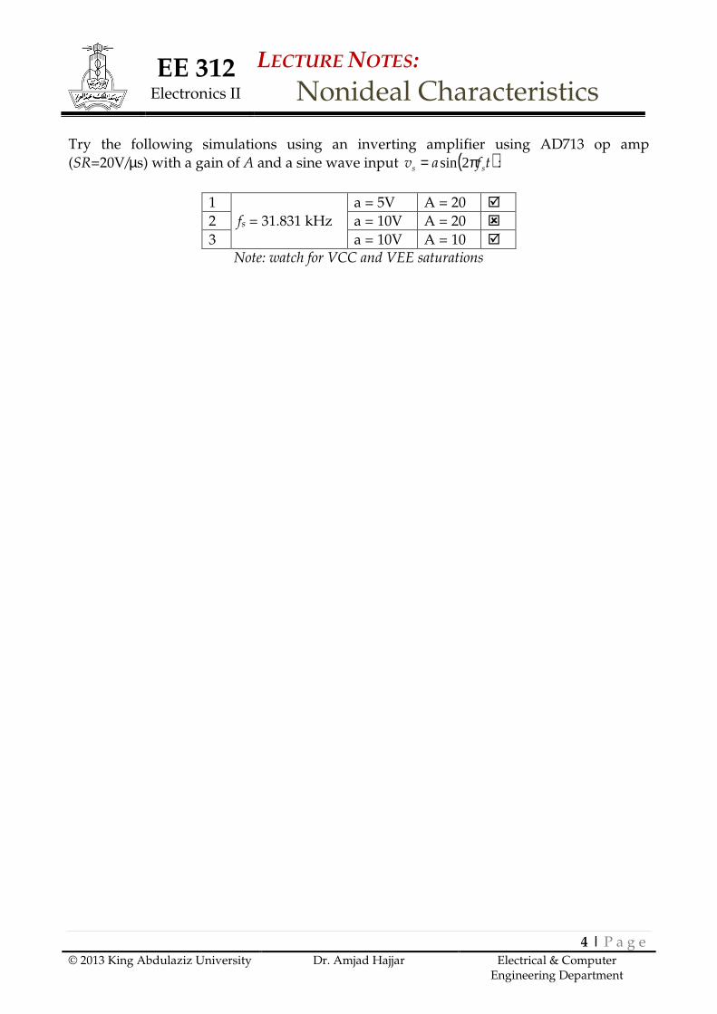
Try the following simulations using an inverting amplifier using AD713 op amp
(fUG=4MHz) with a gain of A and a sine wave input ( )tfav ss π= 2sin :
1 fs = 4 MHz a = 1V A = 1 �
2 fs = 400 kHz a = 1V A = 1 �
3 fs = 400 kHz a = 10V A = 1 �
4 fs = 400 kHz a = 1V A = 10 � Note: watch for VCC and VEE saturations
2.2 SLEW RATE
Op amps cannot make sudden output voltage changes. If a square wave is to be amplified, the voltage change will take time to reach the upper or lower value. Thus:
SRt
vo ≤∆
∆
In the general case, this rate of change is the derivative in time:
SRt
vo ≤∂
∂
where SR is the slew rate of the op amp used. In the designs below, suppose the input signal is ( )tvs 40010 cos= . Determine the minimum op amps slew rate for correct
operation:
( )( )tv
tv
o
o
400sin12000
400cos30
−==
&
thus,
msV
sVSR
12
12000
=≥
Stage I: ( )
( )msVSR
tv
tv
16
400sin16000
400cos40
1
1
≥=
−=&
Stage II:
( )( )
msVSR
tv
t
vv
8
400sin8000
400cos20
5.0
2
12
≥=
−=×=
&
Since all stages must operate:
msVSR 16≥
EE 312 Electronics II
LECTURE NOTES:
Nonideal Characteristics
4 | P a g e
© 2013 King Abdulaziz University Dr. Amjad Hajjar Electrical & Computer Engineering Department
Try the following simulations using an inverting amplifier using AD713 op amp
(SR=20V/µs) with a gain of A and a sine wave input ( )tfav ss π= 2sin :
1
fs = 31.831 kHz
a = 5V A = 20 �
2 a = 10V A = 20 �
3 a = 10V A = 10 � Note: watch for VCC and VEE saturations