no job nametrincavelli/papers/mam10.pdf · effects of the carbon coating and the surface oxide...
TRANSCRIPT
North American Branch 32 Avenue of the Americas New York, NY 10013-2473, USA
PROOFREADING INSTRUCTIONS Tel : 212 337-5978 Fax : 212 337-5959 E-mail: [email protected] Dear Microscopy and Microanalysis Contributor: Attached is a read-only PDF page proof of your introduction/article/review scheduled to be published in:
Microscopy and Microanalysis Please follow these procedures: 1. Proofreading: Proofread your article carefully. This will be your final reading before publication. Check
especially the spellings of names and places as well as the accuracy of dates and numbers. Please answer all queries that may appear on a separate page.
2. Text: Changes in the text are limited to typographical and factual errors. Rewriting or other stylistic changes
are not permitted. Contributors may be charged for excessive author alterations, and publication of your article may be delayed.
3. Corrections: Please respond with an e-mail message to Morrell Gillette at [email protected], identifying
the correction by page number, column, paragraph, and line. Please indicate the present errant copy followed by the correct copy. The corrections to the proofs should be sent within 2 days of receipt. Corrections can also be sent by fax to (212) 337-5959.
4. References: If the query involves a reference entry, please arrange the new entry into the correct format. In
order to prepare the HTML full-text files for online viewing, the complete information including correct spelling of author names, year, titles, publisher, city of publication, page range, and so forth are needed.
5. Figures: Review the figure reproductions on the page proofs to see if important features have been well
represented. If something seems out of order, indicate the errant features in a cover letter. Should it be necessary that new electronic copy of the figures (in PDF, TIFF, or EPS) or text (Word or WordPerfect) will have to be provided, please indicate which application is being used.
6. Offprint Order Form: Complete and return the enclosed Offprint Order Form to the address noted on the form.
Cambridge must receive this form before the journal is printed. You may order offprints or bound issue copies at the authors’ discount of US$12.50 (up to 10 copies). As explained on the offprint order form, a 50% surcharge is levied for late orders. If no offprints are desired, please state this in your response.
7. Delay in response: Please note that failure to respond in a timely fashion may delay publication of your article
or may require publication without your corrections. Thank you for your prompt attention to these proofs. If you have any questions, please feel free to contact Morrell Gillette at (212) 337-5978, or by e-mail: [email protected], or send a fax to (212) 337-5959. Thanks.
Best Regards, Morrell Gillette, Production Editor

OFFPRINT ORDER FORM
Microscopy and Microanalysis Vol.: ______ No.: ________ Author(s): Article Title: Important instructions:
1. Journal contributors must complete this Offprint Order Form and return it to Cambridge so that their orders can be processed. Use this form to order offprints and/or copies of the issue containing your contribution.
2. For co-authored articles, please note that this form is being sent only to the author receiving the page proofs. Accordingly, please be sure that separate order forms for all co-authors are included when returning this form.
3. Please return this form within 14 days. Your order must be received before the printing of the journal to qualify for the prices listed. There is a 50% surcharge for late orders. Return to:
Morrell Gillette Cambridge University Press 32 Avenue of the Americas New York, NY 10013-2473, USA
4. Orders for offprints must be prepaid by check, credit card, or accompanied by an institutional purchase order. Payment must be in US dollars or Canadian dollar equivalent.
6. Canadian customers must add 7% GST. ************************************** ************************************************************ PAYMENT Total amount: US$_________ (Offprints + Issue Copies) [__] Check enclosed PRICE LIST (in US dollars, incl. surface delivery) [__] Purchase order enclosed No. of -------------------------------------------------- pages 25 50 100 150 200 add'l 50s [__] American Express --------------------------------------------------------- 1-8 $85. $127. $168. $211. $254. $33. [__] MasterCard [__] Visa 9-16 102. 152. 203. 254. 303. 42. 17-24 118. 177. 244. 296. 355. 59. 25-32 135. 203. 280. 338. 405. 68. Card No. Exp.Date add'l ___________________________________ 8 pp. 18. 26. 33. 42. 52. 10. Signature For Air Delivery, add 25% to price. Color plates extra.
************************************** ************************************************************
ORDER HERE MAIL OFFPRINTS/ISSUES TO: [___] Air Delivery (add 25%) Copies of the issue @ $12.50 (Authors' discount price) Name Address TOTAL Offprints City State /Prov. Zip ************************************** ************************************************************

QUERIES
||||||1||||||> Please provide article title.
log no. MAM09376q
Effects of the Carbon Coating and the Surface OxideLayer in Electron Probe Microanalysis
Silvina P. Limandri,1,2 Alejo C. Carreras,1,2 and Jorge C. Trincavelli1,2,*
1Facultad de Matemática, Astronomía y Física, Universidad Nacional de Córdoba, 5000 Córdoba, Argentina2Instituto de Física Enrique Gaviola, Consejo Nacional de Investigaciones Científicas y Técnicas de la República Argentina,Córdoba, Argentina
Abstract: Effects related with the attenuation and deflection suffered by an electron beam when it passesthrough a carbon conductive coating and an oxide film layer on the surface of bulk samples are studied byMonte Carlo simulations and energy dispersive spectroscopy with electron excitation. Analytical expressions areprovided for the primary beam energy and intensity losses and for the deflection of the incident electrons inboth layers, in terms of the incidence energy, the film mass thicknesses, and the atomic number of the oxidizedelement. From these analytical expressions, suitable corrections are proposed for the models used to describethe X-ray spectrum of the substrate, including also the contribution of the X-rays generated in the oxide andconductive films and the characteristic X-ray absorption occurring in those layers. The corrections areimplemented in a software program for spectral analysis based on a routine of parameter refinement, and theirinfluence is studied separately in experimental spectra of single-element standards measured at differentexcitation energies. Estimates for the layer thicknesses are also obtained from the spectral fitting procedure.
Key words: electron probe microanalysis, carbon coating, surface oxidation, modeling of X-ray spectra
INTRODUCTION
Image acquisition by scanning electron microscopy ~SEM!and chemical characterization by electron probe microanal-ysis ~EPMA! in samples with low electrical conductivityhave the inconvenience of charge build up. This effectinfluences the generation of secondary and backscatteredelectrons and the excitation of characteristic X-rays. For thisreason, it is usual to apply a conductive coating on thesetypes of materials to avoid the charge effect and to reducethe sample heating.
The elements most commonly used for coating in SEMare carbon, gold, silver, platinum, palladium, and chro-mium. The heavier elements such as gold also have highsecondary electron yields, which improve the image quality.Nevertheless, the main disadvantage of gold and silver coat-ings is their tendency to migrate on the surface of thesample and coalesce into islands or particles that worsen themacroscopic conductivity and mask some fine details of thesurface. For high-resolution images, coatings with smallerparticle size, e.g., platinum or chromium are used. However,even these elements have a measurable grain size for thehighest resolution achievable in SEM ~Suzuki, 2002!. Toimprove the resolving power, osmium coatings are used
because their grain size is smaller and the thickness requiredfor conductivity is around 1 nm, unlike the several nmnecessary for other coating elements.
Carbon is usually the material of choice for microanal-ysis, due to its excellent transparency and electrical conduc-tivity. Other metal coatings absorb significant amounts ofsoft X-rays. Effects occurring in the coating film, such asattenuation and deviation of primary electrons, absorptionof X-rays emitted by the sample, and generation of photons,are often not taken into account in EPMA because theyrequire knowledge of the conductive film thickness, whichis not straightforward. These effects are also produced inthe oxide layer spontaneously grown on metallic species.Thus, in a typical analysis of metallic samples, on thematerial to be analyzed there is an oxide layer upon whichthe conductive coating is deposited.
Several techniques allow measurement of film thick-nesses. They can be classified as destructive, such as crosssections in transmission and scanning electron microscopyand sputter depth profiling ~Hoffmann, 1998!, and nonde-structive, for instance, X-ray photoelectron spectroscopy~XPS! ~Alexander et al., 2002!, X-ray diffraction ~XRD!~Terada et al., 2001!, X-ray fluorescence ~XRF! ~Kolbe et al.,2005!, X-ray reflectometry ~XRR! ~Terada et al., 2001;Thomsen-Schmidt et al., 2004!, ellipsometry ~Liu et al.,1999!, Rutherford backscattering ~RBS! ~Chu et al., 1978!,particle induced X-ray emission ~PIXE! ~Demortier & Rubal-caba Sil, 1996!, quartz crystal microbalance ~QCM! ~Gold-
Received April 16, 2010; accepted June 1, 2010*Corresponding author. E-mail: [email protected]
Microsc. Microanal. 16, 1–11, 2010doi:10.1017/S1431927610093761 MicroscopyAND
Microanalysis© MICROSCOPY SOCIETY OF AMERICA 2010
MAM16~5! 09376 1/11 07/30/10 12:35 am log no. MAM09376
stein et al., 1994!, etc. The main disadvantages associatedwith the nondestructive techniques listed above are relatedto availability, lateral resolution, thickness range of applica-tion, difficulty in data processing, and need of standards.For instance, RBS requires a particle accelerator and in XPSultrahigh vacuum is needed; thus, both techniques are noteasily available and, in addition, they are not accurate forthicknesses lower than 20 nm and greater than 10 nm,respectively. Another disadvantage of RBS is its limitedelemental resolution for small relative atomic number dif-ferences. On the other hand, XRD works properly only forthicknesses greater than 100 nm; the methods involvingXRF and PIXE are based on calibration curves, which mustbe performed for each particular configuration. RegardingXRR and ellipsometry, these techniques have a limitedlateral resolution, particularly around a few mm for thelatter, which also requires a complicated data treatment.Finally, QCM must be previously calibrated using anothertechnique in order to perform an absolute thickness deter-mination ~Bastin & Heijligers, 2000b; Campos et al., 2002!.
X-ray spectra measured in EPMA can be used to deter-mine layer thicknesses in the nanometric range, relevant forthe oxidation layer and the conductive coating usually foundin materials characterization. For instance, calibration curveswere performed by measuring spectra of particular films~Bastin & Heijligers, 2000a, 2000b! or substrates ~Camposet al., 2001, 2002!. Additional efforts were done to achieve ageneral method capable of determining the film thicknessin a film/substrate system with arbitrary composition ~Ky-ser & Murata, 1974; Yakowitz & Newbury, 1976; Bastin &Heijligers, 2000a!. Moreover, some commercial softwarepackages, such as X-FILM ~Merlet, 1995!, MLA ~Bastinet al., 1998!, STRATAGem ~Pouchou & Pichoir, 1990!, andLAYERF ~Pouchou & Pichoir, 1990!, allow determination ofthe film thicknesses and compositions in more complexconfigurations of stratified samples. Each of these softwareprograms assumes a particular model for the ionizationdepth distribution function w~rz! in a bulk specimen.These approaches, broadly, are based on the construction ofa function w~rz! on the basis of fictitious homogeneoussamples. From the integration of this expression for w~rz!along the mass thickness traveled by the electrons in eachlayer and the experimental peak intensities, layer composi-tions and thicknesses are obtained through a complicatediterative process. The method becomes more difficult whenthe same element is present in a film and in the substrate orin more than one layer.
In the present work, the effects produced by a carboncoating and an oxide layer on a bulk metallic substrate werestudied, and their influence in the modeling of spectra wasanalyzed separately. The attenuation and deflection of theincident electron beam in both layers were studied byMonte Carlo simulation. Analytical expressions are pro-vided for the energy and intensity losses of the primarybeam and for the deflection of the incident electrons in acarbon coating film and in an oxide layer grown on a
metallic substrate. From these analytical expressions, suit-able corrections were introduced in a model that predictsthe X-ray spectrum emitted by a sample, including also thecontribution of the X-rays generated in the oxide andconductive films and the characteristic X-ray absorptionoccurring in those layers. The corrections obtained herewere implemented in software for spectral analysis based ona routine of parameter refinement ~Bonetto et al., 2001!,which is intended to determine both layer mass thicknessesand the substrate composition, provided that certain param-eters are well known ~see the Prediction of Spectra subsec-tion!. The corrections proposed were tested in experimentalspectra of single-element standards measured at severalincident energies.
If the effects of both layers on experimental spectra areignored, quantitative analysis could not be reliably per-formed in some cases, such as low incidence energy, thickcarbon, or oxide layers, or analysis using soft characteristicX-rays. In these cases, important errors could be introducedin standardless and conventional analyses when the un-known and standards are not identically coated or oxidized.
METHODS AND MATERIALS
Simulations and Measurements
Effects produced by the carbon conductive coating and thenative oxide layer were studied by means of Monte Carlosimulations. To this purpose, the software package PENE-LOPE, developed by Salvat et al. ~2003!, was used to simu-late an electron beam impinging perpendicularly on aspecimen composed by a carbon layer deposited on anoxide film. Different incidence energies Eo ~3, 6, 9, 12, 15,18, 21, and 27 keV!, carbon thicknesses zC ~5, 10, 30, 60, and100 nm!, and oxide thicknesses zOx ~5, 10, 20, 50, 80, and150 nm! were simulated for oxides of several elements ~Mg,Si, Sc, Cr, Ni, and Zn!. For the thickest layers tested andwhen simulations for Eo � 3 keV resulted in very fewtransmitted electrons, additional simulations were carriedout for Eo � 3.5, 4, 4.5, 5, and 5.5 keV. The assumed massdensities were 2, 3.6, 2.533, 3.86, 5.2, 6.7, and 5.6 g/cm3 forC, MgO, SiO2, Sc2O3, Cr2O3, NiO, and ZnO, respectively. Allof the calculations amounted to more than 1,600 runs inapproximately 300 h of simulation, each of which com-prises several millions of electron trajectories.
Si and Mg X-ray spectra were measured using SPI#02751 standards to test the results obtained by MonteCarlo simulations. Measurements were performed with aLEO 1450VP scanning electron microscope from the Labo-ratorio de Microscopía Electrónica y Microanálisis ~LAB-MEM! of the Universidad Nacional de San Luis, Argentina.This equipment is furnished with an EDAX Genesis 2000energy dispersive spectrometer with a resolution of 129 eVfor the Mn-Ka line ~5.893 keV!. The detector is a Si~Li!SUTW Sapphire with ultrathin polymer window Moxtek
MAM16~5! 09376 2/11 07/30/10 12:35 am Page: 2
2 Silvina P. Limandri et al.
AP3.3 containing a 380 mm thick silicon support structurewith 77% open area and aluminum ohmic contact. Thespectra were measured at Eo � 3, 6, 9, 12, 15, and 18 keV,with a beam current ranging between 1.1 and 1.7 nA duringa live acquisition time of 100 s for each spectrum.
RESULTS AND DISCUSSION
From the point of view of matrix corrections in quantitativeEPMA, four major effects are caused by the coating andoxide films: attenuation of the electron beam current, atten-uation of the electron energy, deflection of the electronbeam, and X-ray attenuation. These effects were studiedseparately by Kato ~2007! and by Osada ~2005!, but only ina few samples.
To study the first three effects, three parameters wereconsidered: the fraction of energy lost by the incidentelectrons fE , the fraction of transmitted electrons fN , andthe average deflection angle u with respect to the incidencedirection. The fourth effect is directly related to both layerthicknesses. The behavior of the parameters considered wasinvestigated as a function of Eo, the total mass thicknessrz � rC zC � rOx zOx , and the sum of the mass thicknessesweighted by the atomic numbers S � rC ZC zC � rOx Zel zOx ,where ri and Zi are the density and the atomic number ofthe material i , respectively; particularly Zel corresponds tothe oxidized element and the subindexes C and Ox corre-spond to the carbon and oxide layers, respectively.
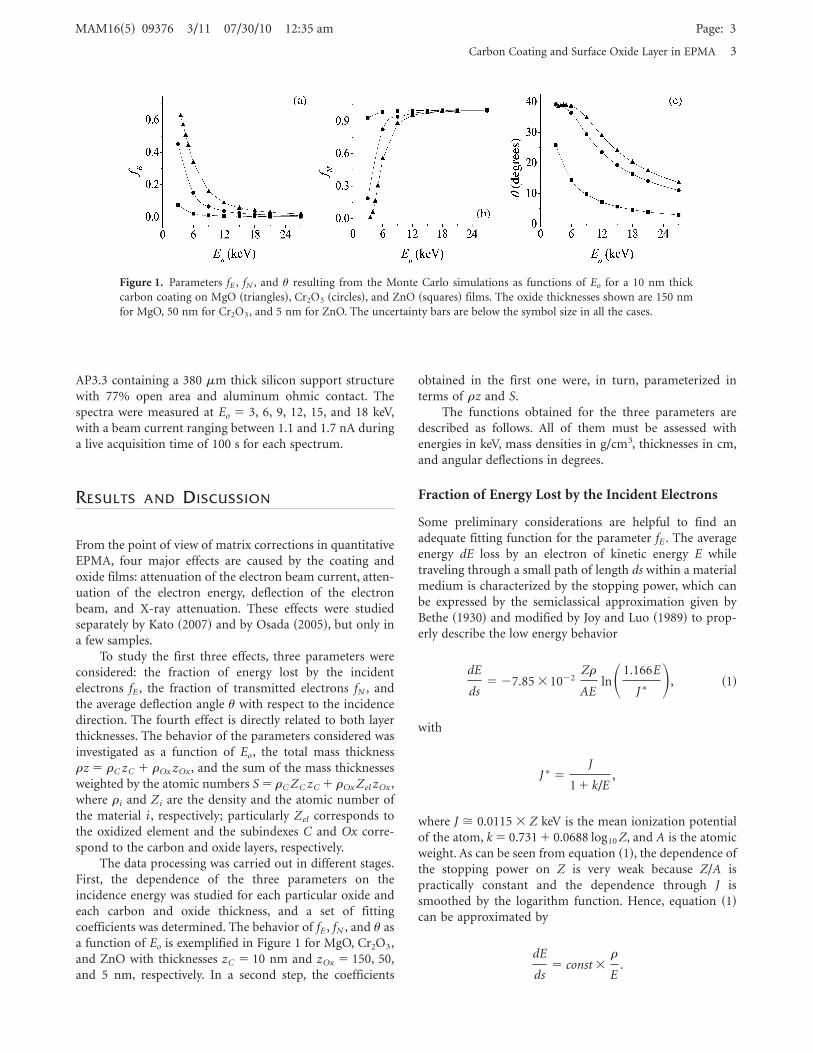
The data processing was carried out in different stages.First, the dependence of the three parameters on theincidence energy was studied for each particular oxide andeach carbon and oxide thickness, and a set of fittingcoefficients was determined. The behavior of fE , fN , and u asa function of Eo is exemplified in Figure 1 for MgO, Cr2O3,and ZnO with thicknesses zC � 10 nm and zOx � 150, 50,and 5 nm, respectively. In a second step, the coefficients
obtained in the first one were, in turn, parameterized interms of rz and S.
The functions obtained for the three parameters aredescribed as follows. All of them must be assessed withenergies in keV, mass densities in g/cm3, thicknesses in cm,and angular deflections in degrees.
Fraction of Energy Lost by the Incident Electrons
Some preliminary considerations are helpful to find anadequate fitting function for the parameter fE . The averageenergy dE loss by an electron of kinetic energy E whiletraveling through a small path of length ds within a materialmedium is characterized by the stopping power, which canbe expressed by the semiclassical approximation given byBethe ~1930! and modified by Joy and Luo ~1989! to prop-erly describe the low energy behavior
dE
ds� �7.85 � 10�2
Zr
AEln�1.166E
J *�, ~1!
with
J * �J
1 � k/E,
where J � 0.0115 � Z keV is the mean ionization potentialof the atom, k � 0.731 � 0.0688 log10 Z, and A is the atomicweight. As can be seen from equation ~1!, the dependence ofthe stopping power on Z is very weak because Z/A ispractically constant and the dependence through J issmoothed by the logarithm function. Hence, equation ~1!can be approximated by
dE
ds� const �
r
E.
Figure 1. Parameters fE , fN , and u resulting from the Monte Carlo simulations as functions of Eo for a 10 nm thickcarbon coating on MgO ~triangles!, Cr2O3 ~circles!, and ZnO ~squares! films. The oxide thicknesses shown are 150 nmfor MgO, 50 nm for Cr2O3, and 5 nm for ZnO. The uncertainty bars are below the symbol size in all the cases.
MAM16~5! 09376 3/11 07/30/10 12:35 am Page: 3
Carbon Coating and Surface Oxide Layer in EPMA 3
Then, the fractional energy loss while crossing a thin layerof thickness z is basically given by
DE
E� const �
rz
E 2. ~2!
Bearing in mind the functional behavior expected, shown inequation ~2!, the expression proposed to fit the simulateddata for fE is
fE �a
b � Eo2
. ~3!
It is important to emphasize that in spite of the simplicityof the fitting function given in equation ~3!, the fitted datacontain all the physics considered in the realistic MonteCarlo package used ~Salvat et al., 2003!.
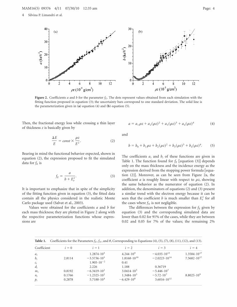
Values were obtained for the coefficients a and b foreach mass thickness; they are plotted in Figure 2 along withthe respective parameterization functions whose expres-sions are
a � a1 rz � a2~rz!2 � a3~rz!3 � a4~rz!4 ~4!
and
b � b0 � b1 rz � b2~rz!2 � b3~rz!3 � b4~rz!4. ~5!
The coefficients ai and bi of these functions are given inTable 1. The function found for fE @equation ~3!# dependsonly on the mass thickness and the incidence energy as theexpression derived from the stopping power formula @equa-tion ~2!# . Moreover, as can be seen from Figure 2a, thecoefficient a is roughly linear with respect to rz, showingthe same behavior as the numerator of equation ~2!. Inaddition, the denominators of equations ~2! and ~3! presenta similar trend with the electron energy because it can beseen that the coefficient b is much smaller than Eo
2 for allthe cases where fN is not negligible.
The differences between the expression for fE given byequation ~3! and the corresponding simulated data arelower than 0.02 for 91% of the cases, while they are between0.02 and 0.05 for 7% of the values; the remaining 2%
Figure 2. Coefficients a and b for the parameter fE . The dots represent values obtained from each simulation with thefitting function proposed in equation ~3!; the uncertainty bars correspond to one standard deviation. The solid line isthe parameterization given in ~a! equation ~4! and ~b! equation ~5!.
Table 1. Coefficients for the Parameters fE , fN , and u, Corresponding to Equations ~4!, ~5!, ~7!, ~8!, ~11!, ~12!, and ~13!.
Coefficient i � 0 i � 1 i � 2 i � 3 i � 4
ai 1.2874{105 4.244{109 �4.035{1013 1.3584{1017
bi 2.8114 �3.5736{105 1.8168{1010 �2.0223{1014 7.5682{1017
ci 1.905{10�2 0.41di 2.226 1.188 0.36719mi 0.8192 �6.3419{102 3.0414{105 �5.446{107
ni 0.1766 �1.2325{102 1.3484{105 �5.72{107 8.8025{109
pi 0.2878 5.7188{104 �6.429{108 3.6016{1012
MAM16~5! 09376 4/11 07/30/10 12:35 am Page: 4
4 Silvina P. Limandri et al.
corresponds to data predicted with differences higher than0.05. It is worth emphasizing that the differences betweenthe values assessed by equation ~3! and the simulated onesdo not present any appreciable trend with the mass thick-ness, although the prediction is slightly worse for low inci-dence energies.
Fraction of Transmitted Electrons
The expression found for the fraction of transmitted elec-trons is given by the attenuation law
fN � max�1 � e�c~Eo�d!
0. ~6!
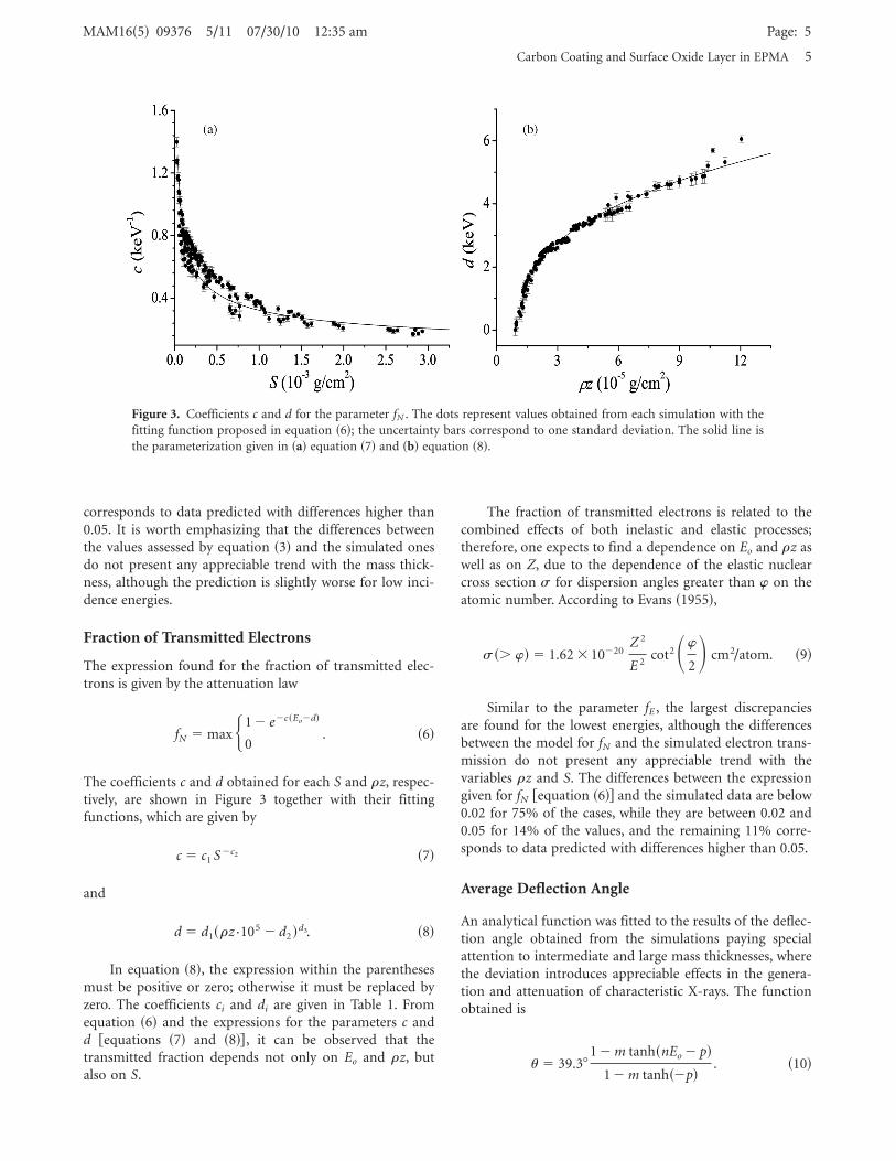
The coefficients c and d obtained for each S and rz, respec-tively, are shown in Figure 3 together with their fittingfunctions, which are given by
c � c1 S�c2 ~7!
and
d � d1~rz{105 � d2 !d3. ~8!
In equation ~8!, the expression within the parenthesesmust be positive or zero; otherwise it must be replaced byzero. The coefficients ci and di are given in Table 1. Fromequation ~6! and the expressions for the parameters c andd @equations ~7! and ~8!# , it can be observed that thetransmitted fraction depends not only on Eo and rz, butalso on S.
The fraction of transmitted electrons is related to thecombined effects of both inelastic and elastic processes;therefore, one expects to find a dependence on Eo and rz aswell as on Z, due to the dependence of the elastic nuclearcross section s for dispersion angles greater than w on theatomic number. According to Evans ~1955!,
s~� w! � 1.62 � 10�20Z 2
E 2cot2�w
2� cm2/atom. ~9!
Similar to the parameter fE , the largest discrepanciesare found for the lowest energies, although the differencesbetween the model for fN and the simulated electron trans-mission do not present any appreciable trend with thevariables rz and S. The differences between the expressiongiven for fN @equation ~6!# and the simulated data are below0.02 for 75% of the cases, while they are between 0.02 and0.05 for 14% of the values, and the remaining 11% corre-sponds to data predicted with differences higher than 0.05.
Average Deflection Angle
An analytical function was fitted to the results of the deflec-tion angle obtained from the simulations paying specialattention to intermediate and large mass thicknesses, wherethe deviation introduces appreciable effects in the genera-tion and attenuation of characteristic X-rays. The functionobtained is
u � 39.381 � m tanh~nEo � p!
1 � m tanh~�p!. ~10!
Figure 3. Coefficients c and d for the parameter fN . The dots represent values obtained from each simulation with thefitting function proposed in equation ~6!; the uncertainty bars correspond to one standard deviation. The solid line isthe parameterization given in ~a! equation ~7! and ~b! equation ~8!.
MAM16~5! 09376 5/11 07/30/10 12:35 am Page: 5
Carbon Coating and Surface Oxide Layer in EPMA 5

The coefficients m and n for each S value, and p for eachmass thickness are plotted in Figure 4 along with therespective parameterization functions whose expressionsare given by
m � m0 � m1 S � m2 S 2 � m3 S 3, ~11!
n � n0 � n1 S � n2 S 2 � n3 S 3 � n4 S 4, ~12!
and
p � p0 � p1 rz � p2~rz!2 � p3~rz!3. ~13!
The coefficients mi , ni , and pi are given in Table 1. Thedeflection angle is mainly determined by the elastic inter-actions @see equation ~9!# . For this reason, the u dependenceon Eo, rz, and S is expected. For large thicknesses or lowincidence energies, equation ~10! tends to the finite value39.3o. The existence of this upper limit can be understoodtaking into account that the mean deflection angle u of thetransmitted electrons can be expressed as
u �
�0
p/2
2pnf f sin f df
�0
p/2
2pnf sin f df
, ~14!
where nf is the number of electrons transmitted with anangle between f and f � df. In the case of isotropicdeflections, nf is a constant, and equation ~14! gives thevalue u � 1 rad ~i.e., 57o!. However, as the isotropizationbegins above the bottom surface, lower deflection angles arefavored because the electrons dispersed at larger anglesmust travel a greater distance inside the layer, before reach-ing the bottom surface. For this reason, the mean deviationangle u resulting from the simulations is lower than the onecorresponding to the isotropic case.
As can be seen from Figure 4, the parameters n and pare poorly predicted by the proposed fitting functions for
low S and rz values, respectively. Nevertheless, these casescorrespond to thin layers, where the influence of u in themodeling of the X-ray spectrum is not important. More-over, the corrections related to this parameter are lessimportant than the ones associated to fN and fE as will bediscussed below. For the whole dataset, the differencesbetween the expression for u given by equation ~10! and thesimulated results are lower than 2o for 78% of the cases,while they are between 28 and 48 for 19% of the values; theremaining 3% corresponds to data predicted with differ-ences higher than 48.
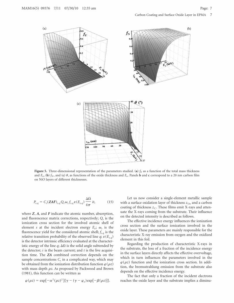
The overall behavior of fE , fN , and u is shown inFigures 5a, 5b, and 5c, respectively. Figure 5a involves all thestudied materials, while Figures 5b and 5c correspond to a20 nm carbon coating on NiO films of different thicknesses,although its behavior is similar to that of the remainingoxides. It can be seen that the transmitted energy fraction~1 � fE ! and the fraction of transmitted electrons fN de-crease with the layer thickness and increase with Eo, asexpected. On the other hand, the deflection angle increaseswith the film thickness, reaching a saturation value asexplained above, whereas it decreases with Eo.
Influence of the Parameters Studiedon the X-Ray Spectra
The effects of the parameters fE , fN , and u due to thepresence of the oxide and conductive carbon layers onexperimental X-ray spectra from single-element specimenswere analyzed by using software for spectral processing inEPMA, based on a parameter optimization method ~Bonettoet al., 2001; Limandri et al., 2008!. This method consists ofminimizing the differences between the experimental spec-trum and an analytical function proposed to describe it.This function takes into account characteristic peaks, brems-strahlung, and different detection artifacts. The detectedcharacteristic intensity Ps,q of the line q from element s inthe sample without neither oxidation film nor conductivecoating is given according to Trincavelli and Van Grieken~1994!
Figure 4. Coefficients m, n, and p for the parameter u. The dots represent values obtained from each simulation withthe fitting function proposed in equation ~10!; the uncertainty bars correspond to one standard deviation. The solid lineis the parameterization given in ~a! equation ~11!, ~b! equation ~12!, and ~c! equation ~13!.
MAM16~5! 09376 6/11 07/30/10 12:35 am Page: 6
6 Silvina P. Limandri et al.
Ps, q � Cs~ZAF!s, q Qs vs fs, q «~Es, q !DV
4pit, ~15!
where Z, A, and F indicate the atomic number, absorption,and fluorescence matrix corrections, respectively; Qs is theionization cross section for the involved atomic shell ofelement s at the incident electron energy Eo; vs is thefluorescence yield for the considered atomic shell; fs,q is therelative transition probability of the observed line q; «~Es,q!is the detector intrinsic efficiency evaluated at the character-istic energy of the line q; DV is the solid angle subtended bythe detector; i is the beam current; and t is the live acquisi-tion time. The ZA combined correction depends on thesample concentrations Cs in a complicated way, which maybe obtained from the ionization distribution function w~rz!with mass depth rz. As proposed by Packwood and Brown~1981!, this function can be written as
w~rz! � exp@�a 2 ~rz!2 #$g � ~g � wo !exp@�b~rz!#%.
Let us now consider a single-element metallic samplewith a surface oxidation layer of thickness zOx and a carboncoating of thickness zC . These films emit X-rays and atten-uate the X-rays coming from the substrate. Their influenceon the detected intensity is described as follows.
The effective incidence energy influences the ionizationcross section and the surface ionization involved in theoxide layer. These parameters are mainly responsible for thecharacteristic X-ray emission from oxygen and the oxidizedelement in this foil.
Regarding the production of characteristic X-rays inthe substrate, the loss of a fraction of the incidence energyin the surface layers directly affects the effective overvoltage,which in turn influences the parameters involved in thew~rz! function and the ionization cross section. In addi-tion, the bremsstrahlung emission from the substrate alsodepends on the effective incidence energy.
The fact that only a fraction of the incident electronsreaches the oxide layer and the substrate implies a diminu-
Figure 5. Three-dimensional representation of the parameters studied. ~a! fE as a function of the total mass thicknessand Eo, ~b! fN , and ~c! u, as functions of the oxide thickness and Eo. Panels b and c correspond to a 20 nm carbon filmon NiO layers of different thicknesses.
MAM16~5! 09376 7/11 07/30/10 12:35 am Page: 7
Carbon Coating and Surface Oxide Layer in EPMA 7

tion of the effective incidence current, which is propor-tional to the intensity of the X-rays emitted by the oxidefilm and the substrate, respectively. On the other hand, thedecrease in the number of electrons reaching the substratemodifies the surface ionization in the oxide layer, whichaffects the X-ray emission of this film.
Due to the departure from the incident direction, the hcoefficient of the sample increases, with a correspondingincrease in the function w~rz! and thus in the intensity ofthe characteristic X-ray emission.
The incidence on the oxide layer is also nonnormal dueto the deflection in the carbon layer. This deviation causestwo effects: an increase in the effective thickness of this layerand, on the other hand, an increment in the number ofelectrons backscattered from it, which in turn produces anenhancement of the oxide film surface ionization wo. Botheffects contribute to a greater generation of O-Ka character-istic photons, as well as to an increase in the characteristicX-rays produced by the metal forming the oxide.
Prediction of Spectra
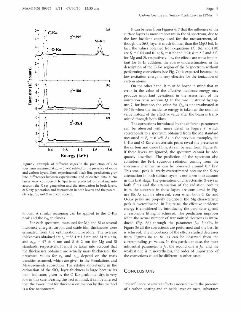
Corrections introduced by the parameters fE , fN , u, and bythe X-ray generation and attenuation in both layers weretested in Si and Mg spectra from pure standards, spontane-ously oxidized and coated with a carbon conductive layer,measured at different excitation energies. To this purpose,the analytical expressions obtained for the corrections wereimplemented in the software based on the parameter opti-mization method mentioned above. Figure 6 shows anexample of the influence of these layers in a Mg spectrummeasured at Eo � 15 keV, whereas Figure 7 exemplifies thesame kind of effects for Si measured at Eo � 3 keV. InFigures 6a, 7a, the layers are completely ignored; as can beseen, the C-Ka and O-Ka peaks are not predicted; inaddition, the characteristic peak produced in the substrateis overestimated mainly because the attenuation in thesurface layers is disregarded. The improvement achievedwhen the attenuation and the contribution of the X-raygeneration taking place in both films is considered can beseen in Figures 6b, 7b. Nevertheless, the prediction is stillincomplete because the effects introduced by the param-eters fE , fN , and u are not taken into account. Finally, whenthe full correction given by equations ~3!, ~6!, and ~10! isconsidered ~Figs. 6c, 7c!, a good description is achieved. Thegoodness of fit is assessed by the parameter x2 defined by
x2 �1
N � NP(
i
~Iiexp � Ii !
2
Iiexp
,
where N is the number of spectral channels, NP is thenumber of parameters to optimize, Ii is the predicted inten-sity corresponding to the channel i , and Ii
exp refers to theexperimental spectrum; the sum runs over all the channelsin the fitted region. As can be seen in Figures 6, 7, the
decrease in x2 indicates an improvement of the spectraldescription when more corrections are introduced.
The intensity predicted for the carbon Ka peak isproportional to zC , to the detector efficiency « at the char-acteristic C-Ka energy, and to other atomic and experimen-tal parameters independent of the photon energy. If accuratethickness determinations are searched, the detector effi-ciency and the remaining parameters must be well known.The model used to calculate the efficiency curve depends onthe characteristic thicknesses of the detector, as explainedby Trincavelli et al. ~2008!. Typically, the efficiency is poorlyknown at low energies because the mass absorption coeffi-cients at this energy range and the detector parameters arenot very well known; however, the product «{zC , requiredto describe the spectrum and eventually to carry out stan-dardless quantification, can be obtained from the minimiza-tion procedure even if the detector efficiency is not well
Figure 6. Example of different stages in the prediction of a Mgspectrum measured at Eo �15 keV, related to the presence of oxideand carbon layers. Dots, experimental; black line, prediction; grayline, differences between experimental and calculated data. a: Nolayers were considered. b: Spectrum predicted only taking intoaccount the X-ray generation and the attenuation in both layers.c: X-ray generation and attenuation in both layers; and the param-eters fE , fN , and u were considered.
MAM16~5! 09376 8/11 07/30/10 12:35 am Page: 8
8 Silvina P. Limandri et al.
known. A similar reasoning can be applied to the O-Kapeak and the zOx thickness.
For each spectrum, measured for Mg and Si at severalincidence energies, carbon and oxide film thicknesses wereestimated from the optimization procedure. The averagethicknesses obtained are zC � 53.161.3 nm and 34 6 4 nm,and zOx � 97 6 4 nm and 8 6 2 nm for Mg and Sistandards, respectively. It must be taken into account thatthe thicknesses obtained are actually mass thicknesses; thepresented values for zC and zOx depend on the massdensities assumed, which are given in the Simulations andMeasurements subsection. The relative uncertainty in theestimation of the SiO2 layer thickness is large because itsmain indicator, given by the O-Ka peak intensity, is verylow in this case. Bearing this fact in mind, it can be inferredthat the lower limit for thickness estimation by this methodis a few nanometers.
It can be seen from Figures 6, 7 that the influence of thesurface layers is more important in the Si spectrum, due tothe low incident energy used for the measurement, al-though the SiO2 layer is much thinner than the MgO foil. Infact, the values obtained from equations ~3!, ~6!, and ~10!are fE � 0.05 and 0.14; fN � 0.99 and 0.94; u � 218 and 318,for Mg and Si, respectively; i.e., the effects are most impor-tant for Si. In addition, the coarse underestimation in thedescription of the C-Ka region of the Si spectrum withoutperforming corrections ~see Fig. 7a! is expected because thelow excitation energy is very effective for the ionization ofcarbon atoms.
On the other hand, it must be borne in mind that anerror in the value of the effective incidence energy mayproduce important deviations in the assessment of theionization cross sections Q. In the case illustrated by Fig-ure 7, for instance, the value for QSi is underestimated at33.5% when the incidence energy is taken as the nominalvalue instead of the effective value after the beam is trans-mitted through both films.
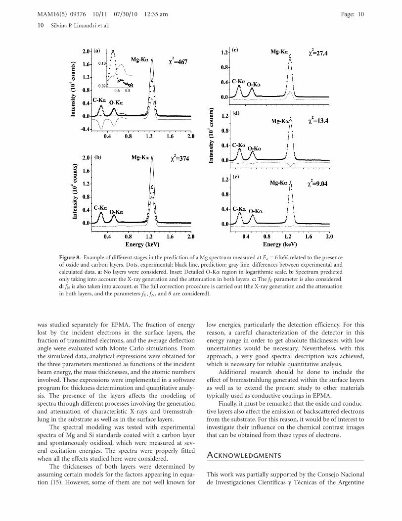
The corrections introduced by the different parameterscan be observed with more detail in Figure 8, whichcorresponds to a spectrum obtained from the Mg standardmeasured at Eo � 6 keV. As in the previous examples, theC-Ka and O-Ka characteristic peaks reveal the presence ofthe carbon and oxide films. As can be seen from Figure 8a,if these layers are ignored, the spectrum cannot be ade-quately described. The prediction of the spectrum alsoconsiders the Fe-L spurious radiation coming from thespecimen chamber, as can be observed around 0.7 keV.This small peak is largely overestimated because the X-rayattenuation in both surface layers is not taken into accountin this first stage. The generation of characteristic X-rays inboth films and the attenuation of the radiation comingfrom the substrate in those layers are considered in Fig-ure 8b. As can be observed, even when both C-Ka andO-Ka peaks are properly described, the Mg characteristicpeak is overestimated. In Figure 8c, the effective incidenceenergy is considered by introducing the parameter fE anda reasonable fitting is achieved. The prediction improveswhen the actual number of transmitted electrons is intro-duced ~Fig. 8d! through the parameter fN . Finally, inFigure 8e all the corrections are performed and the best fitis achieved. The importance of the effects studied decreasesfrom Figures 8a to 8e, as can be observed from thecorresponding x2 values. In this particular case, the mostinfluential parameter is fE , the second one is fN , and theweakest one is u; nevertheless, the order of importance ofthe corrections could be different in other cases.
CONCLUSIONS
The influence of several effects associated with the presenceof a carbon coating and an oxide layer on metal substrates
Figure 7. Example of different stages in the prediction of a Sispectrum measured at Eo � 3 keV, related to the presence of oxideand carbon layers. Dots, experimental; black line, prediction; grayline, differences between experimental and calculated data. a: Nolayers were considered. b: Spectrum predicted only taking intoaccount the X-ray generation and the attenuation in both layers.c: X-ray generation and attenuation in both layers; and the param-eters fE , fN , and u were considered.
MAM16~5! 09376 9/11 07/30/10 12:35 am Page: 9
Carbon Coating and Surface Oxide Layer in EPMA 9
was studied separately for EPMA. The fraction of energylost by the incident electrons in the surface layers, thefraction of transmitted electrons, and the average deflectionangle were evaluated with Monte Carlo simulations. Fromthe simulated data, analytical expressions were obtained forthe three parameters mentioned as functions of the incidentbeam energy, the mass thicknesses, and the atomic numbersinvolved. These expressions were implemented in a softwareprogram for thickness determination and quantitative analy-sis. The presence of the layers affects the modeling ofspectra through different processes involving the generationand attenuation of characteristic X-rays and bremsstrah-lung in the substrate as well as in the surface layers.
The spectral modeling was tested with experimentalspectra of Mg and Si standards coated with a carbon layerand spontaneously oxidized, which were measured at sev-eral excitation energies. The spectra were properly fittedwhen all the effects studied here were considered.
The thicknesses of both layers were determined byassuming certain models for the factors appearing in equa-tion ~15!. However, some of them are not well known for
low energies, particularly the detection efficiency. For thisreason, a careful characterization of the detector in thisenergy range in order to get absolute thicknesses with lowuncertainties would be necessary. Nevertheless, with thisapproach, a very good spectral description was achieved,which is necessary for reliable quantitative analysis.
Additional research should be done to include theeffect of bremsstrahlung generated within the surface layersas well as to extend the present study to other materialstypically used as conductive coatings in EPMA.
Finally, it must be remarked that the oxide and conduc-tive layers also affect the emission of backscattered electronsfrom the substrate. For this reason, it would be of interest toinvestigate their influence on the chemical contrast imagesthat can be obtained from these types of electrons.
ACKNOWLEDGMENTS
This work was partially supported by the Consejo Nacionalde Investigaciones Científicas y Técnicas of the Argentine
Figure 8. Example of different stages in the prediction of a Mg spectrum measured at Eo � 6 keV, related to the presenceof oxide and carbon layers. Dots, experimental; black line, prediction; gray line, differences between experimental andcalculated data. a: No layers were considered. Inset: Detailed O-Ka region in logarithmic scale. b: Spectrum predictedonly taking into account the X-ray generation and the attenuation in both layers. c: The fE parameter is also considered.d: fN is also taken into account. e: The full correction procedure is carried out ~the X-ray generation and the attenuationin both layers, and the parameters fE , fN , and u are considered!.
MAM16~5! 09376 10/11 07/30/10 12:35 am Page: 10
10 Silvina P. Limandri et al.

Republic and the Secretaría de Ciencia y Técnica of theUniversidad Nacional de Córdoba, Argentina.
REFERENCES
Alexander, M.R., Thompson, G.E., Zhou, X., Beamson, G. &Fairley, N. ~2002!. Quantification of oxide film thickness atthe surface of aluminium using XPS. Surf Interface Anal 34,485–489.
Bastin, G.F. & Heijligers, H.J.M. ~2000a!. A systematic databaseof thin-film measurements by EPMA part I—Aluminum films.X-Ray Spectrom 29, 212–238.
Bastin, G.F. & Heijligers, H.J.M. ~2000b!. A systematic databaseof thin-film measurements by EPMA part II—Palladium films.X-Ray Spectrom 29, 373–397.
Bastin, G.F., Dijkstra, J.M., Heijligers, H.J.M. & Klepper, D.~1998!. In Proceedings EMAS’98 3rd Regional Workshop, Llovet,X., Merlet, C. & Salvat, F. ~Eds.!, pp. 25–55. Barcelona: Univer-sitat de Barcelona.
Bethe, H.A. ~1930!. Zur Theorie des Durchgangs schneller Kor-puskularstrahlen durch Materie. Ann Phys 397, 325–400.
Bonetto, R., Castellano, G. & Trincavelli, J. ~2001!. Optimi-zation of parameters in electron probe microanalysis. X-RaySpectrom 30, 313–319.
Campos, C.S., Coleoni, E.A., Trincavelli, J.C., Kaschny, J.,Hubbler, J., Soares, M.R.F. & Vasconcellos, M.A.Z. ~2001!.Metallic thin film thickness determination using electron probemicroanalysis. X-Ray Spectrom 30, 253–259.
Campos, C.S., Vasconcellos, M.A.Z., Llovet, X. & Salvat, F.~2002!. Measurements of L-shell X-ray production cross sec-tions of W, Pt, and Au by 10–30-keV electrons. Phys Rev A 66,012719.
Chu, W., Meyer, J. & Nicolet, M. ~1978!. Backscattering Spectrom-etry. New York: Academic Press.
Demortier, G. & Rubalcaba Sil, J.L. ~1996!. Differential PIXEanalysis of Mesoamerican jewelry items. J Nucl Instrum MethPhys Res B 118, 352–358.
Evans, R.D. ~1955!. The Atomic Nucleus. New York: McGraw-Hill.Goldstein, J.I., Newbury, D.E., Echlin, P., Joy, D.C., Romig,
A.D., Jr., Lyman, C.E., Fiori, C. & Lifshin, E. ~1994!. ScanningElectron Microscopy and X-Ray Microanalysis, 2nd ed. NewYork: Plenum Press.
Hoffmann, S. ~1998!. Sputter depth profile analysis of interfaces.Rep Prog Phys 61, 827–888.
Joy, D.C. & Luo, S. ~1989!. An empirical stopping power relation-ship for low-energy electrons. Scanning 11, 176–180.
Kato, T. ~2007!. Monte Carlo study of quantitative electron probemicroanalysis of monazite with a coating film: Comparison of25 nm carbon and 10 nm gold at E0 � 15 and 25 keV. GeostandGeoanal Res 31, 89–94.
Kolbe M., Beckhoff, B., Krumrey, M. & Ulm, G. ~2005!. Thick-ness determination for Cu and Ni nanolayers: Comparison ofcompletely reference-free fundamental parameter-based X-rayfluorescence analysis and X-ray reflectometry. Spectrochim ActaB 60, 505–510.
Kyser, D.F. & Murata, K. ~1974!. Quantitative electron micro-probe analysis of thin films on substrates. IBM J Res Dev 18,352–363.
Limandri, S., Trincavelli, J., Bonetto R. & Carreras, A. ~2008!.Structure of the Pb, Bi, Th and U M X-ray spectra. Phys Rev A78, 022518.
Liu, C., Erdmann, J. & Macrander, A. ~1999!. In situ spectro-scopic ellipsometry as a surface-sensitive tool to probe thinfilm growth. Thin Solid Films 355, 41–48.
Merlet, C. ~1995!. In Proceedings 29th Annual Conference of theMicrobeam Analysis Society, Etz, E.S. ~Ed.!, p. 203. New York:VHC Publishers.
Osada, Y. ~2005!. Monte Carlo study of quantitative EPMA analy-sis of a nonconducting sample with a coating film. X-RaySpectrom 34, 96–100.
Packwood, R. & Brown, J. ~1981!. A Gaussian expression todescribe w~rz! curves for quantitative electron probe micro-analysis. X-Ray Spectrom 10, 138–146.
Pouchou, J.L. & Pichoir, F. ~1990!. Surface film X-ray microanal-ysis. Scanning 12, 212–224.
Salvat, F., Fernández-Varea, J. & Sempau, J. ~2003!. PENEL-OPE—A code system for Monte Carlo simulation of electronand photon transport. Issy-les-Molineaux, France: OECD/NEAData Bank.
Suzuki, E. ~2002!. High-resolution scanning electron microscopyof immunogold-labelled cells by the use of thin plasma coatingof osmium. J Microsc 208, 153–157.
Terada, S., Murakami, H. & Nishihagi, K. ~2001!. Thickness anddensity measurement for new materials with combined X-raytechnique. SEMICON Europa 2001, Munich, April 23.
Thomsen-Schmidt, P., Hasche, K., Ulm, G., Herrmann, K.,Krumrey, M., Ade, G., Stümpel, J., Busch, I., Schädlich, S.,Schindler, A., Frank, W., Hirsch, D., Procop, M. & Beck, U.~2004!. Realisation and metrological characterisation of thick-ness standards below 100 nm. Appl Phys A 78, 645–649.
Trincavelli, J., Limandri, S., Carreras, A. & Bonetto, R.~2008!. Experimental method to determine the absolute effi-ciency curve of a wavelength dispersive spectrometer. MicroscMicroanal 14, 306–314.
Trincavelli, J. & Van Grieken, R. ~1994!. Peak-to-backgroundmethod for standardless electron microprobe analysis of parti-cles. X-Ray Spectrom 23, 254–260.
Yakowitz, H. & Newbury, D.E. ~1976!. A simple analytical methodfor thin film analysis with massive pure element standards. InProceedings 9th Annual Scanning Electron Microscope Sympo-sium, vol. 1, pp. 151–152. Chicago: IITRI.
MAM16~5! 09376 11/11 07/30/10 12:35 am Page: 11
Carbon Coating and Surface Oxide Layer in EPMA 11
<||||||1||||||