near field wireless power transmission - open...
TRANSCRIPT

Near Field Wireless Power Transmission
Item Type text; Proceedings
Authors Althawab, Meshal; Eberhard, Jared; Hernandez, Alan; Manos,John; Patel, Aniket; Tavour, Alex; von Oppenfeld, Christian
Publisher International Foundation for Telemetering
Journal International Telemetering Conference Proceedings
Rights Copyright © held by the author; distribution rights InternationalFoundation for Telemetering
Download date 07/07/2018 10:14:49
Link to Item http://hdl.handle.net/10150/579582

1
Near Field Wireless Power Transmission
Authors: Althawab, Meshal 520-907-9301 [email protected]
Eberhard, Jared 520-396-8409 [email protected] Hernandez, Alan 520-333-7660 [email protected]
Manos, John 480-399-7557 [email protected] Patel, Aniket 520-254-2961 [email protected]
Tavour, Alex 520-425-2865 [email protected] von Oppenfeld, Christian 602-309-6658 [email protected]
Sponsors/Advisors: Dr. Hao Xin [email protected]
Dr. Michael Marcellin [email protected] Ivar Sanders [email protected]
University of Arizona
Abstract - A prototype wireless power transfer system using the near field to transfer energy between resonantly tuned coils, in order to charge a cell phone or other small electronic device. The system uses resonance to ensure maximum wireless power transfer efficiency between the two coils, and gain greater flexibility in distance between the two coils. The frequency of power transfer is in the unregulated 6.78MHz ISM band. The system is monitored and controlled by an Arduino, and shuts off power when the system does not detect a load.
Keywords – Resonance Coils; Frequency Tuning; Induction;
I. Introduction We created a device that utilizes a tuned pair of Resonant Inductive Circuits which allows for the transmission and
reception of wireless power sufficient to charge a cell phone, while also narrowing the size of the coils to not add significant bulk to the device. The motivation behind this project is directly influenced by distaste of current wireless charging devices on the open market and the use of a newer form of near field wireless power transmission. We improved the overall design of the wireless power device for maximum power efficiency while minimizing the size of the required equipment.
The future applications of this design can be found in the automotive, medical, and consumer electronics industries. Currently transmitting power through the near field wireless field has a few downsides. The major concern is the wasted energy that is dissipated when the signal is transmitted to receiver. Research has shown that many current devices can only output a 70% transfer efficiency. The scope of this project lies in the chance to increase that output transfer efficiency and improve user mobility.
Our mission is to create a prototype near field wireless charging pad, using resonant inductive coupling, which will allow for flexibility in the positioning of the phone and will maximize the power transfer in the system.
II. System Analysis and Design
The idea behind near field wireless power transmission is the use of electrostatic induction. The technology that will be applied in this project is known as resonant inductive coupling. Research has shown this technology to be more reliable and
2
has a better efficiency than pure inductance methods. Both coils will need to be tuned to the same frequency in order for them to resonate efficiently.
A. Research/Analysis At the resonant frequency the reactive components of the circuit, both inductive and capacitive, cancel, resulting in a
purely real power vector, a condition of maximum efficiency. After all as the inductance of the coil grows, a smaller added capacitance is required to tune it to the resonant frequency.
The quality factor or Q of an inductor is the ratio of the power stored in the magnetic field versus the power lost by the inductor at a particular frequency.[1] Therefore, in this project we require Q for each coil to be greater than approximately 100 for each coil in order to have sufficient and efficient power transfer. The resistance term is parasitic in nature, and comes from losses in the wire as a result of heating.
Skin effect is the tendency of an AC current to become distributed within a conductor such that the current density is largest near the surface.[2] Consequently, the resistance of the material to current flow rises as frequency increases. The relative resistivity can be found by the ratio of original cross sectional area with the effective cross-sectional area. The skin effect from the high frequency of the ISM band 6.78MHz increases the resistivity of copper by a factor of 2.7 over the DC resistivity for 18-Gauge wire with a skin depth of 25µm.
The proximity effect occurs between two parallel wires carrying alternating currents. Magnetic fields between wires produce eddy currents, and therefore increase the overall resistance of the wire.[6] This effect increases with a higher frequency, but is difficult to calculate precisely. Consequently the precise value of the quality factor cannot be known before constructing the inductor, because the resistance cannot be known. This is why in planning we must assume that the actual Q will be much lower than the ideal Q.
A comparison between different spiral layouts from the source circuit with inductors revealed that having the highest Q factors relies on the number of loops in the largest enclosed area. However, loops close to the outer edge of the coil contributed to the inductance at a higher rate rather than contributing to resistance. Therefore, this results in more potential energy loss. Parasitic capacitance refers to the extra effect of conductors that act as plates between a dielectric, which is usually air. It becomes a problem with higher frequencies because the very small distributed capacitances that exist will have lower impedances at these frequencies. Due to this effect, there is a voltage difference between each loop of wire in a coil, forming what is effectively a capacitor. This means that each coil cannot be approximated as an RL circuit, but must be modeled as an entire RLC circuit.
The inductance of a planar air-core spiral inductor can be approximated by [2], where r is the average radius of the coil’s turns and d is the distance between the inner radius and outer radius, all in inches. N is the number of turns in the coil, and L is given in µH. This results in a trend where increasing the average radius increases the inductance, while increasing the depth of the coil decreases the inductance, but not as much as adding extra turns increases the inductance.
If the receiver coil is at a certain distance to the transmitter coil, only a fraction of the magnetic flux, which is generated by the transmitter coil, penetrates the receiver coil and contributes to the power transmission. The more flux reaches the receiver; the better the coils are coupled. The grade of coupling is expressed by the coupling factor k. The coupling factor k is a relative measure of the amount of mutual inductance exhibited relative to the inductors which are coupling. K is given by the mutual inductance M divided by the geometric average inductance of the two inductors.
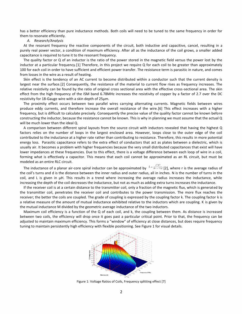
Maximum coil efficiency is a function of the Q of each coil, and k, the coupling between them. As distance is increased between two coils, the efficiency will drop once it goes past a particular critical point. Prior to that, the frequency can be adjusted to maintain maximum efficiency. This forms a “window” of efficiency at close distances, but does require frequency tuning to maintain persistently high efficiency with flexible positioning. See Figure 1 for visual details.
Figure 1: Voltage Ratios of Coils, Frequency splitting effect [7]
3
B. Design Based on our research into the theory behind wireless energy transfer, we decided on a coil system which ended up being
fairly simple. Our goal was to create a set of coils that would have a high Q factor and would allow for the best power transfer efficiency. Our coils would be made of a low-resistance, 18-gauge wire. They have wide spacing, equivalent to 1 turn of 18-gauge wire, between each turn of the wire, in order to keep the proximity effect to a minimum, and ensuring that the parasitic capacitance does not prevent us from tuning each coil to our ISM frequency. Unfortunately, due to the restrictions of the ISM band, we are unable to implement frequency tuning, in order to ensure maximum transmission at all distances. However, we still achieve maximal power efficiency at zero distance, and moderate power efficiency at distances of less than 2 inches.
The design of the system uses an Alternating Current signal (AC) to create a magnetic field in order to transfer energy between the two inductive coils.
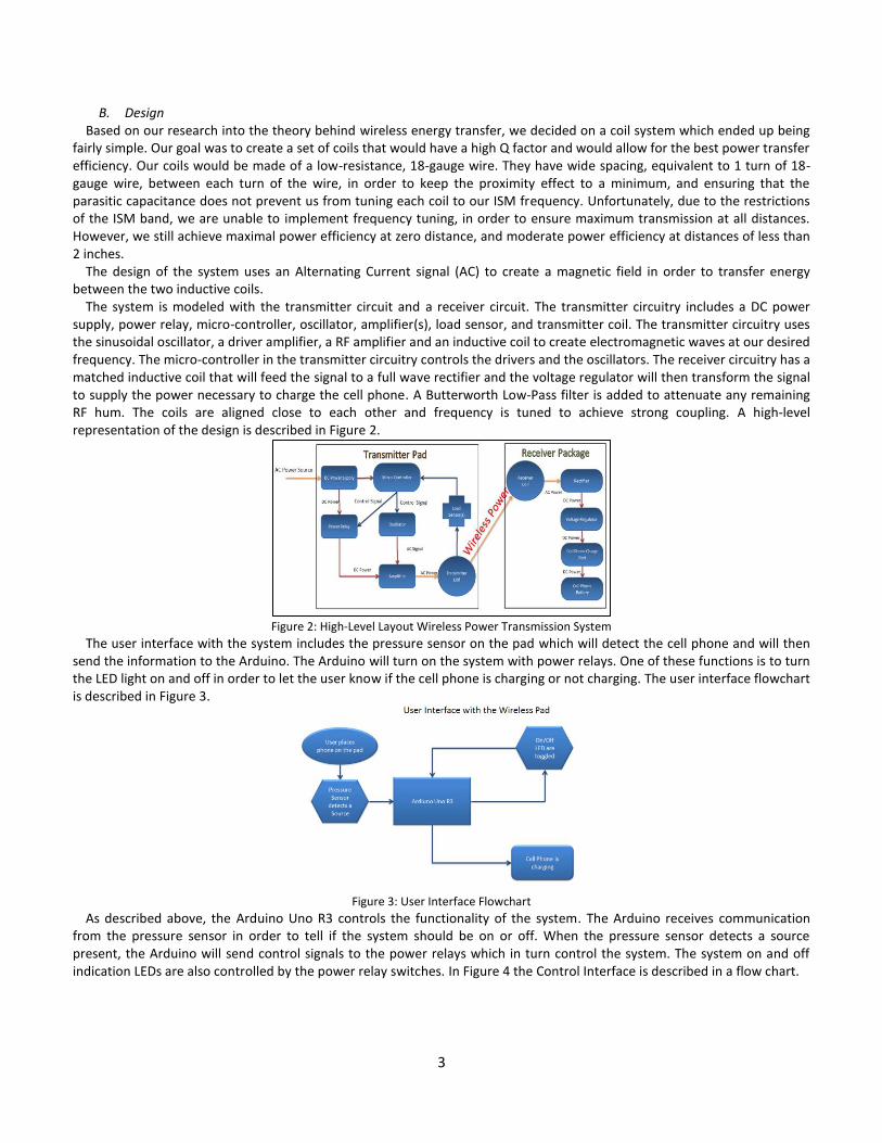
The system is modeled with the transmitter circuit and a receiver circuit. The transmitter circuitry includes a DC power supply, power relay, micro-controller, oscillator, amplifier(s), load sensor, and transmitter coil. The transmitter circuitry uses the sinusoidal oscillator, a driver amplifier, a RF amplifier and an inductive coil to create electromagnetic waves at our desired frequency. The micro-controller in the transmitter circuitry controls the drivers and the oscillators. The receiver circuitry has a matched inductive coil that will feed the signal to a full wave rectifier and the voltage regulator will then transform the signal to supply the power necessary to charge the cell phone. A Butterworth Low-Pass filter is added to attenuate any remaining RF hum. The coils are aligned close to each other and frequency is tuned to achieve strong coupling. A high-level representation of the design is described in Figure 2.
Figure 2: High-Level Layout Wireless Power Transmission System
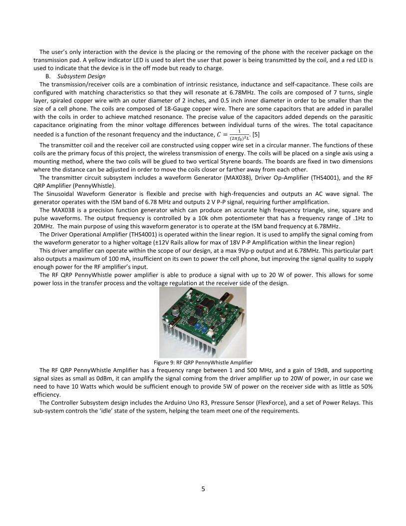
The user interface with the system includes the pressure sensor on the pad which will detect the cell phone and will then send the information to the Arduino. The Arduino will turn on the system with power relays. One of these functions is to turn the LED light on and off in order to let the user know if the cell phone is charging or not charging. The user interface flowchart is described in Figure 3.
Figure 3: User Interface Flowchart
As described above, the Arduino Uno R3 controls the functionality of the system. The Arduino receives communication from the pressure sensor in order to tell if the system should be on or off. When the pressure sensor detects a source present, the Arduino will send control signals to the power relays which in turn control the system. The system on and off indication LEDs are also controlled by the power relay switches. In Figure 4 the Control Interface is described in a flow chart.

4
Figure 4: Software Interface Flowchart
III. Implementation of the System
The system is composed of two superstructures, the transmitter pad and the receiver package. The transmitter pad receives power from the wall, controls and conditions the power to provide AC power to the transmitter coil. The receiver coil picks up the AC power from the transmitter coil, and then converts it into DC power at the voltage necessary to maintain a charge for a lithium ion cell phone battery.
A. Top-Level Design
Figure 5: Schematic of the Transmitter Circuitry
Transmitter circuitry figure (Figure 5) shown above is composed of micro-controller, oscillator, RF amplifier, power relay, pressure sensor, Driver Amplifier, QRP RF Amplifier, and Transmitter coil. Power to the circuit comes from the wall to the microcontroller and then from the microcontroller circuitry to the rest of the transmitter. The microcontroller is controlling three components; two LEDs, a Yellow LED to show the charging state and a Red LED to show it’s in on/off state mode, and the Load Sensor. The Load sensor is used to sense whether the phone has been placed on the pad or not. The Sinusoidal Waveform Generator is used to meet our ISM Band Frequency of 6.78 MHz. The QRP RF Amplifier then amplifies the power up to 10 W to transmitter coil which provides sufficient power on the receiver side.
Figure 6: Schematic of Receiver Circuitry
The Receiver circuitry is composed of receiver coil, a voltage rectifier and voltage regulator. Once the receiver coil receives the power it then converts the AC signal to DC voltage using the Full Wave Rectifier. The voltage regulator takes the DC signal and limits the signal to a max of 5 volts which is then fed into the Cell Phone leads. In order to improve the output efficiency a LDO (Low Drop Out) voltage regulator is used.
5
The user’s only interaction with the device is the placing or the removing of the phone with the receiver package on the transmission pad. A yellow indicator LED is used to alert the user that power is being transmitted by the coil, and a red LED is used to indicate that the device is in the off mode but ready to charge.
B. Subsystem Design The transmission/receiver coils are a combination of intrinsic resistance, inductance and self-capacitance. These coils are
configured with matching characteristics so that they will resonate at 6.78MHz. The coils are composed of 7 turns, single layer, spiraled copper wire with an outer diameter of 2 inches, and 0.5 inch inner diameter in order to be smaller than the size of a cell phone. The coils are composed of 18-Gauge copper wire. There are some capacitors that are added in parallel with the coils in order to achieve matched resonance. The precise value of the capacitors added depends on the parasitic capacitance originating from the minor voltage differences between individual turns of the wires. The total capacitance
needed is a function of the resonant frequency and the inductance,
. [5]
The transmitter coil and the receiver coil are constructed using copper wire set in a circular manner. The functions of these coils are the primary focus of this project, the wireless transmission of energy. The coils will be placed on a single axis using a mounting method, where the two coils will be glued to two vertical Styrene boards. The boards are fixed in two dimensions where the distance can be adjusted in order to move the coils closer or farther away from each other.
The transmitter circuit subsystem includes a waveform Generator (MAX038), Driver Op-Amplifier (THS4001), and the RF QRP Amplifier (PennyWhistle). The Sinusoidal Waveform Generator is flexible and precise with high-frequencies and outputs an AC wave signal. The generator operates with the ISM band of 6.78 MHz and outputs 2 V P-P signal, requiring further amplification.
The MAX038 is a precision function generator which can produce an accurate high frequency triangle, sine, square and pulse waveforms. The output frequency is controlled by a 10k ohm potentiometer that has a frequency range of .1Hz to 20MHz. The main purpose of using this waveform generator is to operate at the ISM band frequency at 6.78MHz.
The Driver Operational Amplifier (THS4001) is operated within the linear region. It is used to amplify the signal coming from the waveform generator to a higher voltage (±12V Rails allow for max of 18V P-P Amplification within the linear region)
This driver amplifier can operate within the scope of our design, at a max 9Vp-p output and at 6.78MHz. This particular part also outputs a maximum of 100 mA, insufficient on its own to power the cell phone, but improving the signal quality to supply enough power for the RF amplifier’s input.
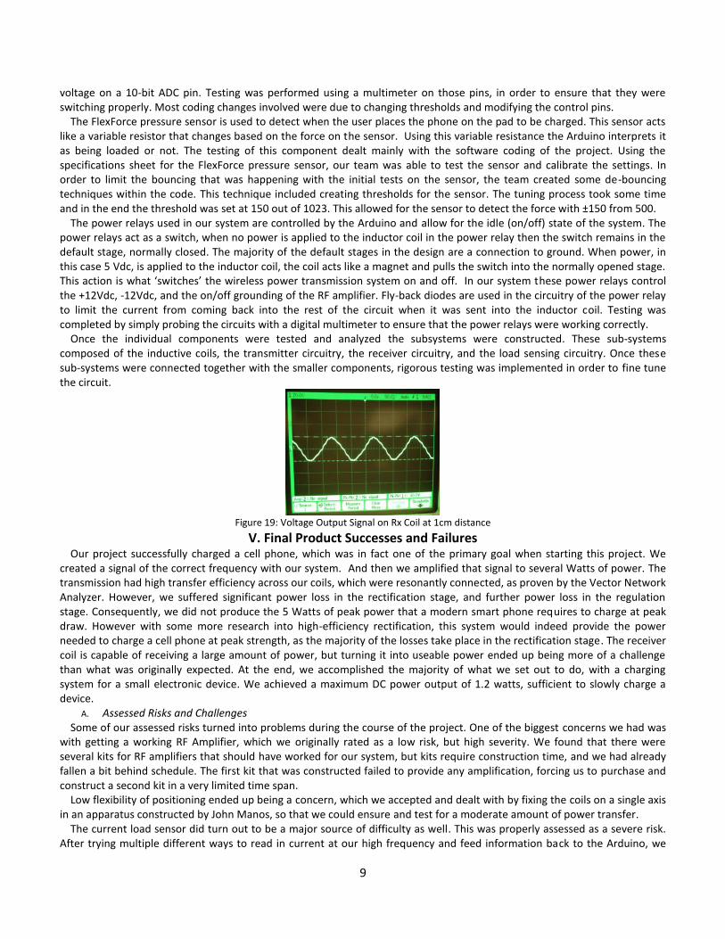
The RF QRP PennyWhistle power amplifier is able to produce a signal with up to 20 W of power. This allows for some power loss in the transfer process and the voltage regulation at the receiver side of the design.
Figure 9: RF QRP PennyWhistle Amplifier
The RF QRP PennyWhistle Amplifier has a frequency range between 1 and 500 MHz, and a gain of 19dB, and supporting signal sizes as small as 0dBm, it can amplify the signal coming from the driver amplifier up to 20W of power, in our case we need to have 10 Watts which would be sufficient enough to provide 5W of power on the receiver side with as little as 50% efficiency.
The Controller Subsystem design includes the Arduino Uno R3, Pressure Sensor (FlexForce), and a set of Power Relays. This sub-system controls the ‘idle’ state of the system, helping the team meet one of the requirements.

6
Figure 10: Arduino Uno R3
Arduino Uno R3, Figure 10, is used to control the driver amplifying transmitting signal, the load sensor, and then the user interface (use of LED lights). The Arduino Uno R3 microcontroller consists of an ATmega328 microcontroller with an operating voltage of 5V. This particular board has 14 Digital I/O pins, of which 6 provide PWM output, and a clock speed of 16 MHz. This product serves as a functional logic base for using the relays with the sensors.
The load sensor reads current at a high sample rate through the coils, and feeds resultant data to the microcontroller. This allows the transmitter coil to detect whether a receiving load is present; allowing the controller to shut off power when nothing is present. The load sensor is also used for functionality testing in frequency range and testing of the pressure sensor.
Figure 11: Force Sensitive Resistor Sensor
Force Sensitive Resistor (FSR) sensor will be used in this design to detect the phone placement. This FSR will vary its resistance depending on how much pressure is being applied to the sensing area. When no pressure is being applied to the FSR, system will be in off mode state. This part will perform the job of detecting when the phone is placed on the pad. The Arduino will control the main functionality of this part and read/interpret the data from the chip.
The power relay is used to toggle between a full-power mode and a no-power state. These control the power available to the oscillator, the driver amplifier and the RF amplifier. They require more current than can be supplied through an Arduino pin, so their drive power is sourced from the Arduino’s 5V power supply, using 2N2222 BJT transistors. A 1N4148 diode is applied in reverse bias across the relay’s power source, to prevent fly-back current from when the relay switches off.
The power relay used in this design is the JZC-11F. This power relay will allow for switching voltages in the receiver circuitry. It controls the power available to the wave form generator. It also controls the input Power for Power Amplifier and power for the Arduino. This part is used because power relays that are already built into the cell phone are not sufficient.
The receiver circuitry subsystem includes a Full-Wave Rectifier (CDBH220L-HF), and a Voltage Regulator (LP38690DT-5V) in series which will in turn supply the power necessary to charge the cell phone.
The Schotkey bridge rectifier takes the AC voltage input and converts it into a single-direction voltage output. An electrolytic capacitor connected to the output and ground charges up to the maximum voltage output from the rectifier, and subsequently helps smooth the ripple out to the amount the capacitor discharges in the span of a single period.
The almost DC power is fed into a linear voltage regulator to bring the voltage down to a constant 5V at up to 1A of current; a form which can be accepted by the voltage input to the cell phone. The linear regulator has a feedback loop to ensure it keeps its output constant, and a final resistor is added to avoid any chance of current overloading the cell phone. The voltage regulator that is used in the design of the receiver circuitry is the LP38690DT-5V/NOPB.
The power characteristics required to charge a battery drop over time. Peak power is only required when the battery is completely discharged, and the battery’s voltage is low. Modeling a battery as circuit components can be complex, but a valid way to model it is as a resistive load which varies with time. As a result of this, by supplying a constant voltage power supply to the load allows the load to self-select its own power-draw. Pload=Vload
2/Rload, and as Rload increases during the battery
charge, the power draw will decrease proportionally. The combination of these subsystems is the core of the project. Each of these subsystems is dependent of each other and
once connected together properly, they form our near field wireless power transfer system.

7
C. Functions of Each Subsystem The transmitter circuitry includes the Arduino, load sensor, AC Signal waveform generator, the driver amplifier, RF amplifier
and the transmitter coil. The AC Signal generator outputs 12 mW, which then feeds the signal into the Driver Op-Amp. The driver amplifier then amplifies the 12 mW signal into a 250 mW signal that will be the input into the RF Amplifier. The RF Amplifier then amplifies the 250 mW signal into approximately an 8 W signal. Finally, the transmitter circuit has the transmitter coil which transmits power through the air into the receiver coil. This transmitter circuitry sends the AC power signal to the receiver coil.
The main function of the load sensor is to find out when the user places his/her cell phone onto the wireless charging pad. The load sensor that has been chosen connects to the circuitry of the transmitter coil and is controlled by the Arduino. The Arduino is programmed to read the load sensor and distinguish when the cell phone is in range for charging. Once the phone has been placed on the wireless charging pad, the Arduino will receive the data from the load sensor and will then turn on indication LED lights so that the user will know the phone is charging. The Arduino will also turn on a separate indication LED light to notify the user that the phone has been successfully charged.
The receiver circuit receives the transmitted power from the transmitter coil. Then, it transforms this AC power signal into a DC power source with the voltage regulator. The DC signal will then be filtered through a voltage rectifier to get a maximum 5 Volt signal on the output. Both the transmitter and Receiver circuits have inductive coils with series capacitance of 500 pF for Self-resonance at 6.78MHz.
Figure 15: Receiver Circuitry and Transmitter Circuitry
IV. Testing of the System
The team tested each of our coil designs with an Impedance Analyzer, which gave us the impedance (Z) of our coil in terms of its resistance (R) and reactance (X), at frequencies we were able to select. We used this information to provide frequency sweeping plots (1 kHz - 10 MHz) of the Q of the coils. We encountered significant drop-off in the rate the Q increased with frequency, which should have been more or less linear. The resistance of the coils turns out to increase dramatically with frequency when the turns are spaced closely. In the end, we discovered that a relatively low inductance was necessary to achieve a high Q value, so long as the resistance was low enough. This is how we were led to our ultimate coil design, the 7-turn 18-gauge 2-inch diameter winding.
Once the coils were constructed, and we had their inductance value measured by the impedance meter, we had to resonantly tune them together. We had the proper inductance values of the coils, however we did not know their precise parasitic capacitance, which meant that in order to find the resonant coupling point, and we had to use trial and error with a Vector Network Analyzer (VNA). Using the VNA to measure transmission across the coils, we were able to use set capacitors of 470pF to get close to the expected values of capacitance, in parallel with a variable trimmer capacitor with values between 5 and 30 pf, which we individually tuned to achieve a maximum transmission efficiency of -0.08dB, which is over 98% efficient, as seen in Figure 16.
Figure 16: Vector Network Analyzer Results

8
The waveform generator was set up according to its datasheet specifications for operating a sinusoidal output. The only substitution we made was to replace a 20kΩ potentiometer which controls the frequency of the output, with a 10kΩ potentiometer, which allowed us to more finely tune its operative frequency. With +5V supplied from the Arduino board, and the -5V from a voltage regulator, the waveform generator outputted a 2Vp-p AC signal at 6.78MHz, as determined by an Oscilloscope 10-to-1 probe. Using a digital multimeter as an ammeter, we found that its resultant current was about 9mA, which meant that it output 12.5mW of power.
The driver operational amplifier was tested under many different conditions, using the function generator as a source. We originally determined that at our frequency of 6.78MHz, the maximum slew rate that the op-amp could support limited us to a gain of 9. Consequently, we used the driver op-amp in an inverting amplifier configuration with a 50Ω and a 450Ω resistor to provide the gain ratio. We used the 50Ω resistor rather than a larger value, because the output of the waveform generator expected a 50Ω load. This however ended up overstraining the op-amp. We changed the rails up to ±12V, which eliminated the clipping that was happening, but we still were having problems with the voltage dipping significantly under load. We learned via various tests and with the help of several technical experts that with numerous resistances that the output current was strictly limited to 100mA, which meant that the voltage would suffer if the resistance was low enough that the current demand increased beyond 100mA.
Our final configuration of the driver amplifier involved a much smaller gain of 4, with a resistance ratio of 100Ω to 400Ω in the inverting amplifier configuration. This allowed it to output an 8Vp-p signal with its maximum current draw of 100mA, producing a signal of approximately 0.3W.
Figure 17: Voltage Output of 50Ohm loaded Driver Amp
The purpose of the RF QRP Amplifier is to take in the 8 V peak-to-peak signal from the Driver Amplifier and then amplify that signal to an 80 V peak-to-peak signal. The RF Amplifier has a 19 db gain when the input signal meets the ideal input power, 1/4W. In the initial testing of the amplifier a 10 ohm power resistor was used. We found that when we connected the output of the amplifier into the rest of the transmitter circuitry that it was amplifying an 8 Vp-p signal into a 50 Vp-p signal. This is a little less than what was expected but we concluded that the power loss was due to some of the components in the transmitter circuitry and that the driver amplifier wasn’t providing 1/4W of power. With the input from the driver amplifier being a little less than 1/4W, we saw that the amplifier had only a 12 db gain. This is still within our operation range so we were fine with the results of the amplifier.
The full-wave rectifier testing was done primarily with a function generator and an oscilloscope probe. The initial tests were done with the rectifier unloaded. We found a significant DC offset, however even these extremely high-frequency rectifiers used couldn’t quite handle the 6.78 MHz frequency. We filtered the signal with a 1000µF capacitor across the output of the Schottkey bridge rectifier. This filtering helped to smooth the signal into more of a DC source.
The Voltage Regulator testing allowed the team to discover that in order to get a constant 5 Vdc out, an input signal of 5.8 Vdc was required. When the regulator was placed in the circuit after the rectifier, the regulator was able to transform the higher voltage signal into a constant 5 Vdc. It was also found that when the rectifier didn’t smooth the AC signal, the voltage regulator would not function correctly. Two 1µf Mylar capacitors were placed in between the ground and Vin, and between ground and Vout to help smooth the input and output signals. When testing for longevity we found that the voltage regulator heated up. Precautions were taken to ensure the voltage regulator would operate for longer periods of time; heat sinks were placed to help dissipate some of this heat.
The Arduino Uno R3 is the microcontroller used to provide the system with a simple method to use logic to control the power state of the system. We connected it to the USB port of a computer in order to program it using the open-source Arduino suite. We set the board to control several digital-out pins to control LEDs and Relays. We set it to read in the sensor
9
voltage on a 10-bit ADC pin. Testing was performed using a multimeter on those pins, in order to ensure that they were switching properly. Most coding changes involved were due to changing thresholds and modifying the control pins.
The FlexForce pressure sensor is used to detect when the user places the phone on the pad to be charged. This sensor acts like a variable resistor that changes based on the force on the sensor. Using this variable resistance the Arduino interprets it as being loaded or not. The testing of this component dealt mainly with the software coding of the project. Using the specifications sheet for the FlexForce pressure sensor, our team was able to test the sensor and calibrate the settings. In order to limit the bouncing that was happening with the initial tests on the sensor, the team created some de-bouncing techniques within the code. This technique included creating thresholds for the sensor. The tuning process took some time and in the end the threshold was set at 150 out of 1023. This allowed for the sensor to detect the force with ±150 from 500.
The power relays used in our system are controlled by the Arduino and allow for the idle (on/off) state of the system. The power relays act as a switch, when no power is applied to the inductor coil in the power relay then the switch remains in the default stage, normally closed. The majority of the default stages in the design are a connection to ground. When power, in this case 5 Vdc, is applied to the inductor coil, the coil acts like a magnet and pulls the switch into the normally opened stage. This action is what ‘switches’ the wireless power transmission system on and off. In our system these power relays control the +12Vdc, -12Vdc, and the on/off grounding of the RF amplifier. Fly-back diodes are used in the circuitry of the power relay to limit the current from coming back into the rest of the circuit when it was sent into the inductor coil. Testing was completed by simply probing the circuits with a digital multimeter to ensure that the power relays were working correctly.
Once the individual components were tested and analyzed the subsystems were constructed. These sub-systems composed of the inductive coils, the transmitter circuitry, the receiver circuitry, and the load sensing circuitry. Once these sub-systems were connected together with the smaller components, rigorous testing was implemented in order to fine tune the circuit.
Figure 19: Voltage Output Signal on Rx Coil at 1cm distance
V. Final Product Successes and Failures
Our project successfully charged a cell phone, which was in fact one of the primary goal when starting this project. We created a signal of the correct frequency with our system. And then we amplified that signal to several Watts of power. The transmission had high transfer efficiency across our coils, which were resonantly connected, as proven by the Vector Network Analyzer. However, we suffered significant power loss in the rectification stage, and further power loss in the regulation stage. Consequently, we did not produce the 5 Watts of peak power that a modern smart phone requires to charge at peak draw. However with some more research into high-efficiency rectification, this system would indeed provide the power needed to charge a cell phone at peak strength, as the majority of the losses take place in the rectification stage. The receiver coil is capable of receiving a large amount of power, but turning it into useable power ended up being more of a challenge than what was originally expected. At the end, we accomplished the majority of what we set out to do, with a charging system for a small electronic device. We achieved a maximum DC power output of 1.2 watts, sufficient to slowly charge a device.
A. Assessed Risks and Challenges
Some of our assessed risks turned into problems during the course of the project. One of the biggest concerns we had was with getting a working RF Amplifier, which we originally rated as a low risk, but high severity. We found that there were several kits for RF amplifiers that should have worked for our system, but kits require construction time, and we had already fallen a bit behind schedule. The first kit that was constructed failed to provide any amplification, forcing us to purchase and construct a second kit in a very limited time span.
Low flexibility of positioning ended up being a concern, which we accepted and dealt with by fixing the coils on a single axis in an apparatus constructed by John Manos, so that we could ensure and test for a moderate amount of power transfer.
The current load sensor did turn out to be a major source of difficulty as well. This was properly assessed as a severe risk. After trying multiple different ways to read in current at our high frequency and feed information back to the Arduino, we
10
settled on a pressure sensor, ignoring current-sensing capabilities altogether. Future improvements could focus on this part of the transmission circuitry, mainly to create a more reliable system for detecting the need to start charging the cell phone.
In many cases, expert knowledge was required for testing. When this happened, the team would look to other sources such as the companies that provided the devices parts and other technical personnel. Our output power did end up being lower than what was expected in the project. We were still able to alter it to fulfill the goal of charging a cell phone; however it will not charge at the same rate as a typical AC-to-USB charger.
In order for our prototype to make it into a marketable form, cost-saving measures could be implemented by integrating most of the transmitter and receiver circuitry on individual printed circuit boards. Space-saving measures are important for the receiver circuit, as it should fit inside of a small electronic device. In our prototype we only worried about the coil size as our primary concern, as they serve as the power bus. Future improvements could take this into consideration and improve the design for a more marketable design. We also recommend choosing the operational frequency after doing some research into the availability of parts that can handle that frequency. Our bandwidth we chose ended up severely limiting our options, forcing us to spend significant amounts of time sourcing new parts, whenever we found a component did not perform as we expected. Ideally this system would be built from parts that work within variable frequencies as to allow for frequency tuning as the distance in the coils changes.
VI. Conclusions
We achieved a system for low-power transfer across a small distance using a coil interface capable of being integrated into a cell phone. The power resulting at the end does not match that of a wall-socket AC-USB inverter; however it does provide power enough to charge a cell phone. The result is a system which will charge a cell phone, albeit at a lower rate than if plugged in directly. We achieved resonant coupling between coils at the ISM band 6.78MHz. In the end, we achieved extremely high transmission efficiency of -0.08dB at close range across the coils. The system successfully transferred power through the Near Field between resonant inductive coils, and conditioned the power output to be suitable for consumer electronics. With power output characteristics similar to that found in most mobile phone chargers, we’ve demonstrated the viability of this technology in providing power to small electronics.
Acknowledgment
The authors wish to thank Dr. Hao Xin, Dr. Michael Marcellin, Wei Hua, and the faculty and staff of the Electrical Engineering Department at the University of Arizona for their technical support.
References [1] Azad, Umar. "Analysis and Experimental Results for an Inductively Coupled Near-Filed Power Transmission System." Department of Electrical Engineering. UCLA, Dec. 2009. Web. [2] Greenhouse, H. M. "Design of Planar Rectangular Microelectronic Inductors." IEEE, June 1974. Web. [3] Gwon, Gwang-Hee. "Wireless Charger Decresed in Variation of Charging Efficiency." Gwon Et Al. Patent Application Publication, 23 Apr. 2009. Web. [4] Kim, Tae-Woong. "Study of Intelligent Battery Charging Using Inductive Transmission of Power and Information." IEEE, Mar. 2000. Web. [5] Li, Ke. "Qi-Ferry: Energy-Constrained Wireless Charging in Wireless Sensor Networks." IEEE, Jan. 2012. Web. [6] Lundquist, Weyman. "Minimize Winding Losses in High Frequency Inductors." West Coast Magnetics. Power Electronics Technology, July 2008. Web. Nov. 2012. [6] Olvitz, L. "Wireless Power Transfer for Mobile Phone Charging Device." Department of Communications. MIPRO, 21 May 2012. Web. [7] Raval, Pratik. "A Wireless Power Transfer System for Low Power Electronics Charging Applications." University of Auckland, Apr. 2008. Web. [8] Teo, Yin Q. "Wireless Power Transmission in the SmartHome." Duke University, Jan. 2010. Web.