near-field optical characterization of gan and inxga1−xn/gan heterostructures grown on...
TRANSCRIPT
ARTICLE IN PRESS
1386-9477/$ - se
doi:10.1016/j.ph
�Correspondi68720785
E-mail addre
(S. Tripathy).
Physica E 25 (2005) 356–365
www.elsevier.com/locate/physe
Near-field optical characterization of GaN and InxGa1�xN/GaN heterostructures grown on freestanding GaN substrates
S.J. Chuaa, S. Tripathya,�, P. Chena, E. Takasukab, M. Uenob
aInstitute of Materials Research and Engineering, 3 Research Link, Singapore 117602, SingaporebItami Rresearch Labs., Sumitomo Electric Industries Ltd., 1-1, Koyakita 1-chome, Itami-shi, Hyogo 664-0016, Japan
Received 14 June 2004; accepted 29 June 2004
Available online 9 September 2004
Abstract
Using near-field scanning optical microscopy (NSOM), we report the spatial distribution of photoluminescence (PL)
intensity in III-nitride-based semiconductor layers grown on GaN substrates. Undoped GaN, In0.11Ga0.89N, and
In0.13Ga0.87N/GaN multi-quantum wells (MQWs) were grown by metal organic chemical vapor deposition (MOCVD)
on freestanding GaN substrates. Micro-Raman spectroscopy has been used to evaluate the crystalline properties of the
GaN homoepitaxial layers. The variation of the PL intensity from the NSOM imaging indicates that the external PL
efficiency fluctuates from 20% to 40% in the 200 nm InGaN single layer on freestanding GaN, whereas it fluctuates
from 20% to 60% in InGaN/GaN MQWs. In the NSOM-PL images, bright island-like features are observed. After
deconvolution with the spatial resolution of the NSOM, the size of these features is estimated to be in the range of
150–250 nm.
r 2004 Elsevier B.V. All rights reserved.
Pacs: 78.30.Fs; 78.55.Cr; 78.66.Fd
Keywords: Near-field scanning optical microscopy (NSOM); Photoluminescence; InGaN/GaN multi-quantum wells
1. Introduction
Despite technological breakthroughs in GaNtechnology, the major obstacle to produce high-
e front matter r 2004 Elsevier B.V. All rights reserve
yse.2004.06.053
ng author. Tel.: +65-68748119; fax: +65-
quality III-nitride materials and devices is the lackof suitable substrates. Although sapphire and SiCare the most commonly used substrates for GaNheteroepitaxy, a high density of dislocationsappears in the III-nitride heteroepitaxial layersdue to large lattice and thermal mismatch. In orderto overcome this problem, several studies haverecently been conducted on GaN based materialsgrown on freestanding bulk GaN substrates [1–3].
d.
ARTICLE IN PRESS
S.J. Chua et al. / Physica E 25 (2005) 356–365 357
Such homoepitaxial growth of GaN films enablesaccurate determination of the electronic bandgap,free-exciton binding energy, effective masses,impurity ionization, etc. The availability of thesehigh-quality GaN substrates with low backgroundimpurity concentration and lower dislocationdensity will have a tremendous impact on the III-nitride-based technologies.
Photoluminescence (PL) is commonly applied toinvestigate optical properties of these nitrides. Inmost micro-PL studies, the absolute PL efficiencyin InGaN/GaN layers shows spatial variationthroughout the wafers. Addition of In to GaNsubstantially increases the quantum efficiency.However, the influence of various defects onluminescence and the recombination dynamics isnot clear in InGaN based materials. It has beensuggested that the strong PL from InGaN/GaNQWs is associated with excitons strongly localizedat potential minima arising from compositionfluctuations and phase segregation [4,5]. Someresearchers have shown that the main radiativerecombination can be attributed to excitonslocalized in the In-rich regions acting as self-assembled QDs [6,7]. Formation of these dotssuppresses the carrier diffusion towards variousdefects and is crucial for lasing in InGaN-basedMQWs. Thus, a systematic microscopic or nano-scopic PL study could provide more informationon the spatial variation of the quantum efficiencyin these nitrides.
Nanoluminescence or nanofluorescence spectro-scopy and imaging techniques are becomingpopular for the investigation of optical propertiesof semiconductor nanomaterials. Conventionalmicro-PL techniques are affected by diffractionphenomenon, which limits the lateral resolution toapproximately 0.6 mm. However, this limitationcan be overcome by near-field scanning opticalmicroscopy (NSOM) where it is possible to achievespatial resolution in the range of 50–100 nm.Recently, this technique has been successfullyapplied to InGaN/GaN MQWs and light emittingdiodes [8–11]. Inhomogeneities in the spatiallymapped luminescence obtained by cathodolumi-nescence (CL) have been attributed to micro-structural defects [12]. NSOM is an alternative toCL and compare to CL, it allows high-spatial
resolution PL measurements with simultaneoustopographic information.In order to retrieve information about the
spatial inhomogeneities in emission patterns ofIII-nitrides, we have carried out NSOM-PLmeasurements on GaN, InGaN, and InGaN/GaN MQWs grown on freestanding GaN sub-strates. For comparison, epilayers were grown onundoped GaN grown on freestanding GaN sub-strates and on undoped GaN grown on sapphire(0 0 0 1). Observations from micro-PL and micro-Raman measurements show that the samplesgrown on freestanding GaN substrates are nearlystrain-free and of high crystalline quality com-pared to those epilayers grown on GaN/sapphire.The spatial pattern of the luminescence wasinvestigated and on the basis of such measure-ments, an optical resolution of about 100–150 nmhas been obtained. We present a systematicanalysis of near ultraviolet and visible NSOM-PL imaging from these homoepitaxial layers andhave compared these results with layers grown onsapphire under identical growth conditions.
2. Experimental
The 400 mm freestanding GaN substrates weregrown by HVPE on GaAs substrate and separatedfrom the substrate by backside etching technique[13,14]. These substrates show n-type conductivity.The GaN templates were mechanically polishedand chemically cleaned. A 2.0 mm GaN was grownon the freestanding GaN substrate by low-pressureMOCVD. This template, known as f-GaN will beused for subsequent device layer growth. For acomparative study, the same thickness of GaN wasalso grown on sapphire and this template is knownas s-GaN. Structural characterization shows thatf-GaN has a much lower dislocation densitycompared to s-GaN. In0.11Ga0.89N epilayers ofthickness 200 nm were grown on both f-GaN ands-GaN. Four periods of In0.13Ga0.87N/GaNMQWs (3 nm wells with 10 nm barriers) with aGaN cap layer were also simultaneously grown onf-GaN and s-GaN. The micro-PL spectra under325 nm excitation were recorded from these layersat room temperature using a Renishaw 2000

ARTICLE IN PRESS
350 400 450 500 550 600
0 1 2 3 4 5 60
10
20
30 FilmSubstrate
I BE/I
YL
ExcitationIntensity (104W/cm2)
YL
Band-edge
(a)
(b)PL
Inte
nsi
ty (
a.u
.)
Wavelength (nm)
Fig. 1. (a) Micro-PL spectrum recorded from 2.0 mm GaN
epilayer grown on freestanding GaN substrate using 325 nm
line excitation from a He–Cd laser. (b) Micro-PL spectrum
from the freestanding GaN substrate. The inset shows the plot
of ratio between the band-edge and YL peak intensity as a
function of excitation intensity.
S.J. Chua et al. / Physica E 25 (2005) 356–365358
micro-Raman PL system. The micro-Ramanspectra from the epilayers under 514.5 nm excita-tion were recorded using a JY-T64000 setup. Thespatial resolution during micro-Raman measure-ments was 1.0 mm with a spectral resolution of0.2 cm�1.
The NSOM instrument is configured for ultra-violet-visible imaging at room temperature (RT) inthe reflection mode. A commercial scanner (Na-nonics NSOM) and Cr-Al coated bent near-fieldfiber probes (tip aperture of about 50, 100, and200 nm) obtained from Nanonics Imaging Ltdwere used. The Nanonics/Topaz electronics andquartz software were used for experiment controland data acquisition. This configuration results inan optical resolution determined by the size of theaperture and the distance from the surface, not bythe wavelength of the light source. The NSOMscan head is mounted on a Zeiss upright micro-scope. A He–Cd laser delivering output powerupto 30mW at 325 nm was used as an excitationsource. The light from the laser source wascoupled to the imaging probes by means of alaser-to-fiber coupler. The distance between thesample surface and the NSOM tip is controlled bya normal force feedback system. The scatteredlight from the sample surface is collected in the farfield by a 50�UV-visible microscope objectiveand detected by a photomultiplier tube (PMT) oran avalanche photodiode (APD). Spatial maps ofthe PL intensity can be measured with the fixeddetection energy of the photomultiplier tube.Specific optical short-pass filters were used toblock the light from the diode laser used fordistance regulation. To spectrally analyze thedetected PL light, selected band pass and edgefilters were used along the optical path tothe detector, placed close to the collection optics.The sample mounted on the NSOM piezo-scannerwas scanned at a constant speed of 0.2 mm/s in thelateral direction and longer scanning time (upto1 h per image) was employed to record the PLmaps. The external quantum efficiency was deter-mined from the normalized PL intensity and bycomparing the measured PL from sample withrespect to reading from the scattered laser lightfrom the perfect white Lambertian reflector. Forsuch normalized intensity calibration, the trans-
mission efficiency of all the filters is also taken intoaccount.
3. Results and discussion
Fig. 1 shows the RT micro-PL spectra recordedfrom the GaN epilayer grown on freestandingsubstrate (f-GaN) and from the freestanding GaNsubstrate. The film and the substrate show strongband-edge emission near 363.4 and 365 nm,respectively. The yellow luminescence (YL) at550 nm is much stronger from the substrate. Inthe inset of Fig. 1, we have shown the plot of ratiobetween the band-edge and YL peak intensity as afunction of excitation intensity. As expected, theYL intensity is relatively stronger at low-excitationintensity in both the film and the substrate. Theproperties of the f-GaN are very similar to that ofs-GaN except that the low and RT PL peaks aremuch stronger and narrower in f-GaN. In addi-tion, the PL peaks were at lower energies due torelaxation of the strain and these spectra demon-strate the high quality of the f-GaN suitable forIII-nitride device structures. As expected, the RTPL line width of the f-GaN is also much narrowerthan the corresponding PL line width of the

ARTICLE IN PRESS
200 400 600 800 1000
(b)
(a)
DA
E2
low
LPP- LPP+
A1(LO)
E2(TO)
Inte
nsi
ty (
a.u
.)
Raman shift (cm-1)
Fig. 3. (a) Micro-Raman spectrum recorded from 2.0mm GaN
layer grown on freestanding GaN substrate uisng 514.5 nm line
excitation from an Ar+ laser. (b) Micro-Raman spectrum
recorded from the freestanding GaN substrate.
S.J. Chua et al. / Physica E 25 (2005) 356–365 359
freestanding substrates and shows that the broad-ening due to impurities, dislocations and pointdefects, is greatly reduced. The difference in the PLpeak position between the film and the substratecan be related to the significantly higher carrierconcentration in freestanding GaN substrate (asthe lattice mismatch is negligible). Fig. 2 shows themicro-PL spectra of InGaN layers grown simulta-neously on f-GaN and s-GaN. A strong PL peakcentered at around 400 nm can be observed fromboth the samples. However, the lineshape of thePL spectrum from InGaN grown on s-GaN isasymmetric due to multiple peaks originating frominterference. The much stronger and symmetricGaussian PL line shape of the layer on f-GaNshows improved crystalline quality.
Fig. 3 shows micro-Raman spectra of f-GaN.The spectrum from the GaN film is dominated bythe E2(TO) and A1(LO) phonons located at 567.4and 734 cm�1, whereas the spectrum from thefreestanding GaN substrate is dominated by E2
and the much broader LO-phonon plasmon modes(LPP) centered at 350 and 830 cm�1. The filmshows strong A1(LO) phonon whereas this isabsent in case of the substrate. The observationof LPP+ (830 cm�1) and LPP� (350 cm�1) modesshows that the free carrier plasma interacts withthe A1(LO) phonon, resulting in a mixed pho-non–plasmon mode. These peaks can be seen in all
350 400 450 500 550 600
(b)
(a)
PL
Inte
nsi
ty (
a.u
.)
Wavelength (nm)
Fig. 2. (a) Micro-PL spectrum of 200 nm InGaN layer grown f-
GaN. (b) Micro-PL spectrum of 200 nm InGaN layer grown on
s-GaN.
spectra because of the larger Raman probingdepth. These mixed modes have frequencies whichdepend on the free-carrier concentration and gainintensity at the expense of the A1(LO) phonons.The LPP modes from the freestanding GaNsubstrate imply a free-carrier concentration inexcess of 5� 1018 cm�3 and could be due to highdensity of background oxygen [15]. From f-GaN,the fitting of the uncoupled A1(LO) phonon givesrise to a free carrier concentration of about2� 1017 cm�3. In addition, other modes at 310and 420 cm�1 are also observed from the free-standing GaN substrate. The mode near 310 cm�1
occurs due to the disorder-activated Ramanscattering. This mode, which arises due to thelattice disorder, has been assigned to the highestacoustic-phonon branch at the Brillouin zoneboundary [16]. However, origin of the mode near420 cm�1 is still not clear. It could be associatedwith a higher-order zone-boundary acoustic pho-non in GaN, which is prominent due to impuritiesand disorder present in the substrate. We have alsocarried out cross-sectional Raman mapping, whichshows that the two broad LPP bands near 350 and830 cm�1 originate from the substrate and notfrom the film. Micro-Raman technique has alsobeen used to quantify the strain in f-GaN. The

ARTICLE IN PRESS
S.J. Chua et al. / Physica E 25 (2005) 356–365360
difference of 0.2 cm�1 in the E2 phonon energy(567.4 cm�1 from substrate and 567.2 cm�1 fromthe film) from the cross-sectional mapping clearlyshows that mapping clearly shows that the epilayeris nearly strain-free [17]. The E2 phonon line widthof about 3.2 cm�1 at RT represents high crystallinequality of f-GaN.
Fig. 4 shows the ultraviolet NSOM-PL intensityimages of undoped GaN layer grown on GaNsubstrate. The images from the substrates are alsoshown. The color scale for each image is indicatedat the right. The band-edge and the yellowluminescence (YL) were excited from the samespot on the sample. We have carried out lumines-cence mapping at different detection energies toestablish different spatial origin of the PL emis-sions. Two specific band-pass filters were used totransmit either the band-edge (355–375 nm) or theyellow luminescence (540–560 nm) intensity. From
Fig. 4. 4� 4 mm2 NSOM-PL intensity images of undoped GaN grown
aperture of 200 nm. The images from the substrate are also shown.
550 nm.
the undoped layer, the normalized PL intensity ofband-edge transition fluctuates from 1.8 to 2.2over an area of 4 mm� 4 mm and the YL peakfluctuates from 0.2 to 0.9. From the substrate, theband-edge PL fluctuates from 1.6 to 2.7 and YLfluctuates from 0.8 to 2.2. Such imaging also showsthat YL intensity is much stronger from thesubstrate. Because of the low excitation intensitydue to NSOM probing, the YL is of the sameorder of magnitude relative to the band edge fromboth the film and the substrate. This is evidentfrom the inset of Fig. 1, where we have shown theplot of ratio between the band-edge and YL peakintensity as a function of excitation intensity. Inthe NSOM images, the PL of both the transitionsshow intensity fluctuation occurring within sub-wavelength resolution. Images of the YL from thesubstrate show island-like emission pattern, whichare homogeneously distributed while images of the
on freestanding GaN substrate recorded with a near-field probe
(a) Band-edge PL intensity image at 365 nm. (b) YL image at

ARTICLE IN PRESS
Fig. 5. 10� 10 mm2 NSOM-PL intensity images at 400 nm for
InGaN layers recorded with a near-field probe aperture of
100 nm. (a) InGaN layer grown on f-GaN. (b) InGaN layer
grown on s-GaN.
S.J. Chua et al. / Physica E 25 (2005) 356–365 361
band-edge show few localized bright islands. In allthe images, the band-edge PL which forms theuniform background, shows much stronger PLintensity than YL with modulations o10% overan area of 4 mm� 4 mm. From an estimate of thePL probing depth, it is clear that NSOM signalcomes only from the top layer. The band-edge PLintensity variation may not be due to localordering of defects or nonradiative centers. Spatialvariation of background free carriers may lead tospatially varying PL intensity. Since this variationis much stronger in the substrate, the band-edgePL fluctuates much more than that of the film(from 1.6 to 2.7). It is likely that strong YL fromthe substrate originates from background impur-ity-vacancy complexes decorated along disloca-tions. Cathodoluminescence studies have shownthat the YL in GaN is enhanced at certainpositions presumably due to large number ofextended defects at the surface [18]. The incor-poration of residual impurities in the structurallydefective areas results in localized states that couldlead to appearance of strong yellow luminescencefrom the substrate.
When the tip scans over the sample surface, withheight variation 410 nm, topography-inducedartifacts may appear, which results from a varia-tion of distance regulation. By repeated measure-ments and correlating the topographic andluminescence images under the normal force feed-back technique, we have found that all the imagesare artifact free. The rms roughness of the surfaceof GaN and InGaN layer measured by the NSOMinstrument was as small as 1.6 nm within thescanning region of 5� 5 mm2. Therefore, thefluctuation of PL intensity is not contributed bythe scattered light from the surface. We have alsoexamined the reflection NSOM image, using aband-pass filter to transmit the laser light, tocorrelate the NSOM-topography. From suchmeasurements, we conclude that there is nocorrelation between the reflected NSOM imageand luminescence NSOM image. Hence, it is clearthat surface topography has no effects on the PLproperties and these NSOM PL images suggestinhomogeneous distribution of nonradiative re-combination centers associated with various de-fects in the GaN layers. We believe that such
defects are probably dislocation centers or va-cancy-impurity complexes.Fig. 5 shows the NSOM-PL intensity image of
200 nm InGaN layer grown on f-GaN. The imageclearly shows uniform distribution of PL, with fewisland-like regions. The spatially averaged externalPL efficiency in the layer fluctuates from 20% to40% in the area of 10 mm� 10 mm scanning, whichis as expected from InGaN. To compare thespatial distribution of the PL intensity, we havealso shown the NSOM-PL intensity image fromInGaN grown on s-GaN. Both of these InGaNsamples were grown simultaneously. The InGaN

ARTICLE IN PRESS
S.J. Chua et al. / Physica E 25 (2005) 356–365362
layer on s-GaN also shows a similar variation ofPL intensity and island-like bright spots, butsignificant variation in the external PL efficiencyfrom 15% to 50% has been observed. Thiscomparison shows strong evidence that dislocationdensity and defects reduction in InGaN grown onf-GaN has led to a more uniform PL intensitydistribution. We believe that the PL efficiencyvariation of InGaN on f-GaN is probably due tofluctuation in carrier density, composition, anddislocation density. Also at maximum PL intensity(peak at 400 nm), the bright red islands and themuch weaker blue background differ by 20% inintensity on the film on f-GaN, while these featureson s-GaN differ by 40% in intensity. Therefore, itmay be possible that apart from dislocations,strong strain-induced clustering and compositionfluctuation occurring in InGaN on s-GaN couldlead to an increase in the maximum value of PLintensity (3.3 in InGaN on s-GaN compared to 3.1in InGaN on f-GaN).
Fig. 6 shows the micro-PL spectra and theNSOM-PL image of the In0.13Ga0.87N/GaNMQWs grown on f-GaN. The NSOM topographyfor a 10 mm� 10 mm scanning area is also shown inthis figure. The room temperature PL shows adominant peak near 395 nm. Bright spots within1 mm� 1 mm scanned area are clearly observed inthe NSOM-PL image. From 5 mm� 5 mm scannedNSOM-PL images (not shown), we have observedthat the background PL intensity starts from 2.4 tothe normalized peak intensity of 3.9 with abackground intensity modulation of 15%. Re-peated NSOM measurements show that spatiallyaveraged external PL efficiency fluctuates from20% to 60% in InGaN/GaN MQWs. For acomparative analysis, we have also shown themicro-PL spectrum and NSOM-PL intensity im-age of In0.13Ga0.87N/GaN MQWs grown on s-GaN under identical growth conditions. The PLspectrum shows a blue shift in MQWs grown ons-GaN and such a shift could be due to strain-induced In composition fluctuation. The NSOM-PL intensity shows similar nanoscopic features inthese two samples. However, in the sample grownon sapphire the bright spots are slightly smaller indimension. In both the samples, we believe that thebackground PL comes from InGaN QWs whereas
PL from islands in the range of 200–300 nm maynot be due to In composition fluctuation butpossibly due to formation of InGaN-like quantumdots at the interfaces. In the micro-PL spectrashown in Fig. 6, the emission may arise from boththe well and the dots. We have observed that thebright red color islands are more uniformlydistributed over the yellow color background.The weaker PL intensity (yellow color back-ground) may have originated from the opticallyactive background luminescence of quantum wells,which are excited simultaneously. Even if theNSOM probe is located above the surface of thefirst capped QW-layer containing InGaN dots,luminescence at the detection energy still comesout from the underlying wells. As the NSOMspatial resolution is not less than 50 nm, themodulation in intensity may be due to thedistribution of QDs located at the multi-quantumwell interfaces. In other words, stronger andweaker regions in the PL intensity images maycorrespond to islands with higher and lowerabsolute number of QDs.In case of InGaN/GaN MQWs grown on both
f-GaN and s-GaN, the spatially averaged PLefficiency is 40% and this is much lower thanexpected. Therefore, carrier diffusion may havetaken place during NSOM scanning of the surfaceand nonradiative recombination centers may con-tribute to the RT PL. In addition, high-resolutiontopographic AFM measurements using a DINanoscope setup show very few V-pits in theInGaN layer and InGaN/GaN MQWs grown onf-GaN. Since V-pits originate from screw-disloca-tions, therefore, the formation of nonradiativerecombination is much lower in the films grown onf-GaN compared to films grown on s-GaN. TheNSOM surface topographic images show noelongated islands. It is reported that InGaN grownunder specific growth conditions represent densearrays of InN-rich nanodomains with size in therange of 3–5 nm and density between 1011 and1012 cm�2 [19,20]. There could be variation inthe values of size and content in InGaN nano-domains and their uniformity strongly depend onthe growth parameters. Thus, we expect corre-sponding changes in the NSOM-PL images fromMQWs grown on f-GaN and s-GaN.
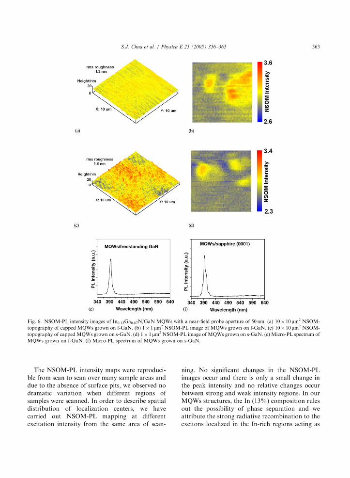
ARTICLE IN PRESS
Fig. 6. NSOM-PL intensity images of In0.13Ga0.87N/GaN MQWs with a near-field probe aperture of 50 nm. (a) 10� 10mm2 NSOM-
topography of capped MQWs grown on f-GaN. (b) 1� 1 mm2 NSOM-PL image of MQWs grown on f-GaN. (c) 10� 10mm2 NSOM-
topography of capped MQWs grown on s-GaN. (d) 1� 1mm2 NSOM-PL image of MQWs grown on s-GaN. (e) Micro-PL spectrum of
MQWs grown on f-GaN. (f) Micro-PL spectrum of MQWs grown on s-GaN.
S.J. Chua et al. / Physica E 25 (2005) 356–365 363
The NSOM-PL intensity maps were reproduci-ble from scan to scan over many sample areas anddue to the absence of surface pits, we observed nodramatic variation when different regions ofsamples were scanned. In order to describe spatialdistribution of localization centers, we havecarried out NSOM-PL mapping at differentexcitation intensity from the same area of scan-
ning. No significant changes in the NSOM-PLimages occur and there is only a small change inthe peak intensity and no relative changes occurbetween strong and weak intensity regions. In ourMQWs structures, the In (13%) composition rulesout the possibility of phase separation and weattribute the strong radiative recombination to theexcitons localized in the In-rich regions acting as

ARTICLE IN PRESS
S.J. Chua et al. / Physica E 25 (2005) 356–365364
self-assembled QDs. It is difficult to obtain NSOMPL intensity image from a single QD with thespatial resolution of this system. Although noindividual In clustering has been detected inInGaN layer and in InGaN/GaN MQWs, thesmall variation in PL intensity of these layers onf-GaN compared to those grown on s-GaN,clearly demonstrate the suitability of III-nitridelight emitting devices on f-GaN. In summary,based on our results, NSOM is found to be usefulto investigate optical properties of III-nitrides andfrom the near-field optical images, luminescencefeatures with 200 nm FWHM have been clearlyresolved on the surface and the size of thesefeatures after deconvolution with the spatialresolution of the NSOM scanning, is estimatedto be in the range of 150–250 nm.
4. Conclusions
GaN, In0.11Ga0.89N, and In0.13Ga0.87N/GaNMQWs were grown by MOCVD on freestandingGaN substrates. High-resolution PL spectra mea-sured from these samples showed high-qualityGaN and InGaN films, which are nearly strainfree. Micro-Raman spectra show significant im-provement in the crystalline quality of GaN grownon freestanding GaN substrates. We have studiedthe nanoluminescence features of these layers bymeans of near-field scanning optical microscopywith a spatial resolution of about 100–150 nm. Theinhomogeneous distribution of the PL in GaNlayer could be due to the nonuniform distributionof the defects or structural imperfection such asdislocations. The luminescence spatial patterns ofInGaN and InGaN/GaN MQWs can be wellcorrelated with the micro-PL properties. Thebright regions in the NSOM images represent PLintensity from the strain-induced clusters orquantum dots formed at the interface of themulti-layers.
References
[1] C.R. Miskys, M.K. Kelly, O. Ambacher, G. Martınez-
Criado, M. Stutzmann, Appl. Phys. Lett. 77 (2000) 1858;
G. Martınez-Criado, C.R. Miskys, A. Cros, O. Ambacher,
M. Stutzmann, J. Appl. Phys. 90 (2001) 5627.
[2] C.Q. Chen, M.E. Gaevski, W.H. Sun, E. Kuokstis,
J.P. Zhang, R.S.Q. Fareed, H.M. Wang, J.W. Yang, G.
Simin, M.A. Khan, H.P. Maruska, D.W. Hill, M.M.C.
Chou,
B. Chai, Appl. Phys. Lett. 81 (2002) 3194.
[3] M.A. Reshchikov, D. Huang, F. Yun, L. He, H. Morkoc,
D.C. Reynolds, S.S. Park, K.Y. Lee, Appl. Phys. Lett. 79
(2001) 3779.
[4] S. Chichibu, T. Azuhata, T. Sota, S. Nakamura, Appl.
Phys. Lett. 69 (1996) 4188;
Y. Narukawa, Y. Kawakami, M. Funato, S. Fujita,
S. Fujita, S. Nakamura, Appl. Phys. Lett. 70 (1997) 981;
Y. Kawakami, K. Omae, A. Kaneta, K. Okamoto,
Y. Narukawa, T. Mukai, S. Fujita, J. Phys.: Condens.
Matter 13 (2001) 6993.
[5] P. Waltereit, O. Brandt, K.H. Ploog, M.A. Tagliente,
L. Tapfer, Phys. Rev. B 66 (2002) 165322;
B. Yang, O. Brandt, B. Jenichen, J. Mullhauser,
K.H. Ploog, J. Appl. Phys. 82 (1997) 1918.
[6] K.P. O’Donnel, R.W. Martin, P.G. Middleton, Phys. Rev.
Lett. 82 (1999) 237.
[7] I.L. Krestnikov, N.N. Ledentsov, A. Hoffmann,
D. Bimberg, A.V. Sakharov, W.V. Lundin, A.F. Tsatsul’-
nikov, A.S. Usikov, Z.I. Alferov, Y.G. Musikhin,
D. Gerthsen, Phys. Rev. B 66 (2002) 155310.
[8] P.A. Crowell, D.K. Young, S. Keller, E.L. Hu,
D.D. Awschalom, Appl. Phys. Lett. 72 (1998) 927.
[9] A. Vertikov, M. Kuball, A.V. Nurmikko, Y. Chen,
S.Y. Wang, Appl. Phys. Lett. 72 (1998) 2645.
[10] M.S. Jeong, J.Y. Kim, Y.W. Kim, J.O. White, E.K. Suh,
C.H. Hong, H.J. Lee, Appl. Phys. Lett. 79 (2001)
976.
[11] A. Kaneta, K. Okamoto, Y. Kawakami, S. Fujita,
G. Marutsuki, Y. Narukawa, T. Mukai, Appl. Phys. Lett.
81 (2002) 4353;
A. Kaneta, T. Izumi, K. Okamoto, Y. Kawakami,
S. Fujita, Y. Narita, T. Inoue, T. Mukai, Jpn. J. Appl.
Phys. Part 1 40 (2001) 110.
[12] S. Chichibu, K. Wada, S. Nakamura, Appl. Phys. Lett. 71
(1997) 2346;
X. Zhang, D.H. Rich, J.T. Kobayashi, J.T. Kobayashi,
P.D. Dapkus, Appl. Phys. Lett. 73 (1998) 1430.
[13] K. Motoki, T. Okahisa, N. Matsumoto, M. Matsushima,
H. Kimura, H. Kasai, K. Takemoto, K. Uematsu,
T. Hirano, M. Nakayama, S. Nakahata, M. Ueno,
D. Hara, Y. Kumagai, A. Koukitu, H. Seki, Jpn. J. Appl.
Phys. 40 (2001) L140.
[14] K. Motoki, T. Okahisa, S. Nakahata, N. Matsumoto,
H. Kimura, H. Kasai, K. Takemoto, K. Uematsu, M.
Ueno, Y. Kumagai, A. Koukitu, H. Seki, J. Cryst. Growth
237–239 (2002) 912.
[15] T. Kozawa, T. Kachi, H. Kano, T. Yaga, M. Hashimoto,
N. Koide, K. Manabe, J. Appl. Phys. 75 (1994) 1098;
H. Harima, H. Sanashita, S. Nakashima, Mater. Sci.
Forum 264–268 (1998) 1369.

ARTICLE IN PRESS
S.J. Chua et al. / Physica E 25 (2005) 356–365 365
[16] W. Limmer, W. Ritter, R. Sauer, B. Mensching, C. Liu,
B. Rauschenbach, Appl. Phys. Lett. 72 (1998) 2589.
[17] The relationship between in plane stress (s) and Raman
shift, Do=4.2s cm�1 GPa–1, has been taken from
the article reported by Kisielowski et al. Phys. Rev. B
54 (1996) 17745 and our observed shift shows that
epilayers grown on freestanding GaN substrates are
strain free.
[18] E. Oh, S.K. Lee, S.S. Park, K.Y. Lee, I.J. Song, J.Y. Han,
Appl. Phys. Lett. 78 (2001) 273.
[19] N.N. Ledentsov, Z.I. Alferov, I.L. Krestnikov, W.V.
Lundin, A.V. Sakharov, I.P. soshnikov, A.F. Tsatsul’ni-
kov, D. Bimberg, A. Hoffmann, Comp. Semicond. 5 (9)
(1999) 61.
[20] H. Chen, R.M. Feenstra, J.E. Northrup, T. Zywietz,
J. Neugebauer, Phys. Rev. Lett. 85 (2000) 1902.