ncp1397 - high performance resonant mode controller with
TRANSCRIPT

© Semiconductor Components Industries, LLC, 2015
October, 2015 − Rev. 61 Publication Order Number:
NCP1397/D
NCP1397A/B, NCV1397A/B
High Performance ResonantMode Controller withIntegrated High-VoltageDrivers
The NCP1397 is a high performance controller that can be utilizedin half bridge resonant topologies such as series resonant, parallelresonant and LLC resonant converters. It integrates 600 V gatedrivers, simplifying layout and reducing external component count.With its unique architecture, including a 500 kHz Voltage ControlledOscillator whose control mode permits flexibility when an ORingfunction is required, the NCP1397 delivers everything needed to builda reliable and rugged resonant mode power supply.
The NCP1397 provides a suite of protection features withconfigurable settings to optimize any application. These include:auto−recovery or fault latch−off, brown−out, open optocoupler,soft−start and short−circuit protection. Deadtime is also adjustable toovercome shoot through current.
Features• High−Frequency Operation from 50 kHz up to 500 kHz
• 600 V High−Voltage Floating Driver
• Adjustable Minimum Switching Frequency with ±3% Accuracy
• Adjustable Deadtime from 100 ns to 2 �s.
• Startup Sequence Via an Externally Adjustable Soft−Start
• Brown−Out Protection for a Simpler PFC Association
• Latched Input for Severe Fault Conditions, e.g. Over Temperature or OVP
• Timer−Based Input with Auto−Recovery Operation for DelayedEvent Reaction
• Latched Overcurrent Protection
• Disable Input for Immediate Event Reaction or Simple ON/OFFControl
• VCC Operation up to 20 V
• Low Startup Current of 300 �A
• 1 A/0.5 A Peak Current Sink/Source Drive Capability
• Common Collector Optocoupler Connection for Easier ORing
• Optional Common Emitter Optocoupler Connection
• Internal Temperature Shutdown
• NCV Prefix for Automotive and Other Applications RequiringUnique Site and Control Change Requirements; AEC−Q100Qualified and PPAP Capable
• These Devices are Pb−Free, Halogen Free/BFR Free and are RoHSCompliant
Typical Applications• Flat Panel Display Power Converters
• High Power ac−dc Adapters for Notebooks
• Computing Power Supplies
• Industrial and Medical Power Sources
• Offline Battery Chargers
PIN CONNECTIONS
MARKING DIAGRAMS
x = P (standard) or V (automotive)y = A or BA = Assembly LocationWL = Wafer LotY = YearWW = Work WeekG = Pb−Free Package
SO−16, LESS PIN 13D SUFFIX
CASE 751AM
1
16
1
2
3
4
5
6
7
8
16
15
14
12
11
10
9
(Top View)
BO
CSS(dis)
Fmax
Ctimer
Rt
FB
DT
Skip/Disable
Vboot
Mupper
VCC
Mlower
Fault
HB
GND
See detailed ordering and shipping information in the packagedimensions section on page 26 of this data sheet.
ORDERING INFORMATION
1
16
NCx1397yGAWLYWW
www.onsemi.com
NCP1397A/B, NCV1397A/B
www.onsemi.com2
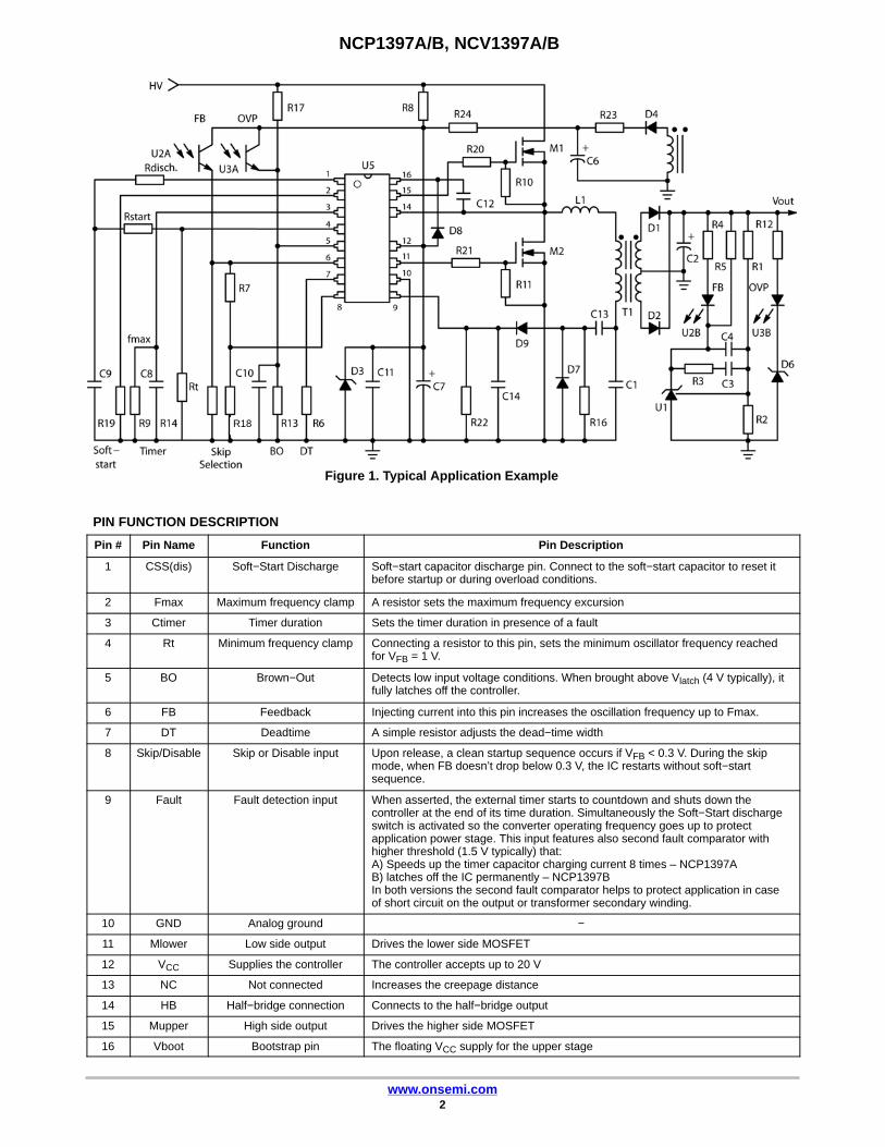
Figure 1. Typical Application Example
R18
PIN FUNCTION DESCRIPTION
Pin # Pin Name Function Pin Description
1 CSS(dis) Soft−Start Discharge Soft−start capacitor discharge pin. Connect to the soft−start capacitor to reset itbefore startup or during overload conditions.
2 Fmax Maximum frequency clamp A resistor sets the maximum frequency excursion
3 Ctimer Timer duration Sets the timer duration in presence of a fault
4 Rt Minimum frequency clamp Connecting a resistor to this pin, sets the minimum oscillator frequency reachedfor VFB = 1 V.
5 BO Brown−Out Detects low input voltage conditions. When brought above Vlatch (4 V typically), itfully latches off the controller.
6 FB Feedback Injecting current into this pin increases the oscillation frequency up to Fmax.
7 DT Deadtime A simple resistor adjusts the dead−time width
8 Skip/Disable Skip or Disable input Upon release, a clean startup sequence occurs if VFB < 0.3 V. During the skipmode, when FB doesn’t drop below 0.3 V, the IC restarts without soft−startsequence.
9 Fault Fault detection input When asserted, the external timer starts to countdown and shuts down thecontroller at the end of its time duration. Simultaneously the Soft−Start dischargeswitch is activated so the converter operating frequency goes up to protectapplication power stage. This input features also second fault comparator withhigher threshold (1.5 V typically) that:A) Speeds up the timer capacitor charging current 8 times – NCP1397AB) latches off the IC permanently – NCP1397BIn both versions the second fault comparator helps to protect application in caseof short circuit on the output or transformer secondary winding.
10 GND Analog ground −
11 Mlower Low side output Drives the lower side MOSFET
12 VCC Supplies the controller The controller accepts up to 20 V
13 NC Not connected Increases the creepage distance
14 HB Half−bridge connection Connects to the half−bridge output
15 Mupper High side output Drives the higher side MOSFET
16 Vboot Bootstrap pin The floating VCC supply for the upper stage

NCP1397A/B, NCV1397A/B
www.onsemi.com3
Figure 2. Internal Circuit Architecture (NCP1397A)
Vref
Rt
VDD
C IDT
−−
+
+
DT Adj.
I = Imax for Vfb = 5.3 VI = 0 for Vfb < Vfb(min)
IminVFB � VFB(o )
Vref
VDD
ImaxVFB = 5
Fmax
VDD
Itimer1
−−
+Timer
+Vref
PON Reset
Vtimer OFFReset
SS(dis)
FB
RFB
−−+
+VFB(fault)
−−
+G = 1
> 0 onlyV=V (FB) −− VFB(min)
IDT
Vref
VDD
+
VFB(min)
DTDeadtime
AdjustmentVDD
−−
+BO
+VBO
−−
+
+Vlatch
Clk
D
S
Q
Q
R
S
Q Q
R PON Reset
50% DC
TemperatureShutdown
VC
CM
anagement
PONReset
Fault
TimeoutFault
Vref
BOReset
FF
+
−−
+Vref Skip/Disable
Skip/Disable
VCC
TimeoutFault
Fault
Mlower
GND
IBO
20 ns NoiseFilter
+
−−
Fault
+Vref(fault)
NC
VBOOT
Mupper
HB
UVLO
FastFault
+
−−+
Vref(OCP)
Vdd
Itimer2
LevelShifter
20 ms NoiseFilter
Fault
PON Reset
Enable(if Vfb<0.3V)
20 ms NoiseFilter
1 ms NoiseFilter

NCP1397A/B, NCV1397A/B
www.onsemi.com4
Figure 3. Internal Circuit Architecture (NCP1397B)
Vref
Rt
VDD
C IDT
−−
+
+
DT Adj.
I = Imax for Vfb = 5.3 VI = 0 for Vfb < Vfb_min
Vref
IminVFB � VFB(o )
Vref
VDD
ImaxVfb = 5
Fmax
VDD
Itimer1
If FAULT Itimer else 0
−−+Timer
+Vref
SS(dis)
FB
RFB
−−+
+VFB(fault)
−−
+G = 1
> 0 onlyV=V (FB) −− VFB(min)
IDT
Vref
VDD
+
VFB(min)
DTDeadtime
AdjustmentVDD
−−
+BO
+VBO
−−
+
+Vlatch
Clk
D
S
Q
Q
R
S
Q Q
R PON Reset
50% DC
TemperatureShutdown
VC
CM
anagement
PONReset
Fault
TimeoutFault
Vref
BOReset
FF
+
−−
+Vref Skip
Skip/Disable
VCC
TimeoutFault
Fault
Mlower
GND
IBO
20 ns NoiseFilter
+
−−
Fault
+Vref(fault)
NC
VBOOT
Mupper
HB
UVLO
LevelShifter
FastFault
+
−−+
Vref(OCP)
PON Reset
Vtimer OFFReset
Fault
PON Reset
Enable(if Vfb<0.3V)
20 ms NoiseFilter
20 ms NoiseFilter
1 ms NoiseFilter

NCP1397A/B, NCV1397A/B
www.onsemi.com5
MAXIMUM RATINGS
Rating Symbol Value Unit
High Voltage bridge pin, pin 14 VBRIDGE −1 to 600 V
Floating supply voltage, ground referenced VBOOT − VBRIDGE 0 to 20 V
High side output voltage VDRV(HI) VBRIDGE−0.3 toVBOOT+0.3
V
Low side output voltage VDRV(LO) −0.3 to VCC+0.3 V
Allowable output slew rate dVBRIDGE/dt 50 V/ns
Power Supply voltage, pin 12 VCC 20 V
Maximum voltage, all pins (except pin 11 and 10) − −0.3 to 10 V
Thermal Resistance Junction−to−Air, SOIC version R�JA 130 °C/W
Storage Temperature Range − −60 to +150 °C
ESD Capability, Human Body Model (HBM) (All pins except HV pins) − 2 kV
ESD Capability, Machine Model (MM) − 200 V
Stresses exceeding those listed in the Maximum Ratings table may damage the device. If any of these limits are exceeded, device functionalityshould not be assumed, damage may occur and reliability may be affected.1. This device(s) contains ESD protection and exceeds the following tests:
Human Body Model 2000 V per JEDEC Standard JESD22−A114EMachine Model 200 V per JEDEC Standard JESD22−A115−A
2. This device meets latchup tests defined by JEDEC Standard JESD78.

NCP1397A/B, NCV1397A/B
www.onsemi.com6
ELECTRICAL CHARACTERISTICS (For typical values TJ = 25°C, for min/max values TJ = −40°C to +125°C, Max TJ = 150°C, VCC = 12 V unless otherwise noted)
Symbol Rating Pin Min Typ Max Unit
SUPPLY SECTION
VCC(on) Turn−on threshold level, VCC going up 12 9.7 10.5 11.3 V
VCC(min) Minimum operating voltage after turn−on 12 8.7 9.5 10.3 V
Vboot(on) Startup voltage on the floating section 16−14 8 9 10 V
Vboot(min) Cutoff voltage on the floating section 16−14 7.4 8.4 9.4 V
Istartup Startup current, VCC < VCC(on) 12 − − 300 �A
VCC(reset) VCC level at which the internal logic gets reset 12 − 6.6 − V
ICC1 Internal IC consumption, no output load on pin 15/14 – 11/10,FSW = 300 kHz
12 − 4 − mA
ICC2 Internal IC consumption, 1 nF output load on pin 15/14 – 11/10,FSW = 300 kHz
12 − 11 − mA
ICC3 Consumption in fault or disable mode (All drivers disabled,Rt = 34 k�, RDT = 10 k�)
12 − 1.5 − mA
VOLTAGE CONTROL OSCILLATOR (VCO)
FSW(min) Minimum switching frequency, Rt = 34 k� on pin 4, Vpin6 = 0.8 V,DT = 300 ns
4 58.2 60 61.8 kHz
FSW(max) Maximum switching frequency, Rf(max) = 1.9 k� on pin 2, Vpin6 >5.3 V, Rt = 34 k�, DT = 300 ns
2 440 500 560 kHz
FBSW Feedback pin swing above which �f = 0 6 − 5.3 − V
DC Operating duty−cycle symmetry 11−15 48 50 52 %
Tdel1 Delay before driver restart from fault or disable mode − − 700 − ns
Tdel2 Delay before driver restart after VCC(on) event (Note 4) − − 11 − �s
Vref(Rt) Reference voltage for Rt pin 4 2.18 2.3 2.42 V
FEEDBACK SECTION
RFB Internal pulldown resistor 6 − 20 − k�
VFB(min) Voltage on pin 6 below which the FB level has no VCO action 6 − 1.1 − V
VFB(off) Voltage on pin 6 below which the controller considers the FB fault 6 240 280 320 mV
VFBoff(hyste) Feedback fault comparator hysteresis 6 − 45 − mV
DRIVE OUTPUT
Tr Output voltage risetime @ CL = 1 nF, 10−90% of output signal 15−14/11−10 − 40 − ns
Tf Output voltage falltime @ CL = 1 nF, 10−90% of output signal 15−14/11−10 − 20 − ns
ROH Source resistance 15−14/11−10 − 13 − �
ROL Sink resistance 15−14/11−10 − 5.5 − �
Tdead Deadtime with RDT = 10 k� from pin 7 to GND 7 250 290 340 ns
Tdead(max) Maximum deadtime with RDT = 82 k� from pin 7 to GND 7 − 2 − �s
Tdead(min) Minimum deadtime, RDT = 3 k� from pin 7 to GND 7 − 100 − ns
IHV(LEAK) Leakage current on high voltage pins to GND 14, 15,16 − − 5 �A
Product parametric performance is indicated in the Electrical Characteristics for the listed test conditions, unless otherwise noted. Productperformance may not be indicated by the Electrical Characteristics if operated under different conditions.3. The IC does not activate soft−start (unless the feedback pin voltage is below 0.3 V) when the skip/disable input is released, this is for skip
cycle implementation.4. Guaranteed by design.

NCP1397A/B, NCV1397A/B
www.onsemi.com7
ELECTRICAL CHARACTERISTICS (continued)(For typical values TJ = 25°C, for min/max values TJ = −40°C to +125°C, Max TJ = 150°C, VCC = 12 V unless otherwise noted)
Symbol UnitMaxTypMinPinRating
TIMERS
Itimer1 Timer capacitor charge current during feedback fault or whenVref(fault) < Vpin9 < Vref(OCP)
3 150 175 190 �A
Itimer2 Timer capacitor charge current when Vpin9 > Vref(OCP) (Icharge1 +Icharge2) – A version only
3 1.1 1.3 1.5 mA
Ttimer Timer duration with a 1 �F capacitor and a 1 M� resistor, Itimer1current applied
3 − 24 − ms
TtimerR Timer recurrence in permanent fault, same values as above 3 − 1.4 − s
Vtimer(on) Voltage at which pin 3 stops output pulses 3 3.8 4 4.2 V
Vtimer(off) Voltage at which pin 3 restarts output pulses 3 0.95 1 1.05 V
RSS(dis) Soft−start discharge switch channel resistance 1 − 100 − �
PROTECTION
Vref(Skip) Reference voltage for Skip/Disable input (Note 4) 8 630 660 690 mV
Hyste(Skip) Hysteresis for Skip/Disable (Note 4) 8 − 45 − mV
Vref(Fault) Reference voltage for Fault comparator 9 0.99 1.04 1.09 V
Hyste(Fault) Hysteresis for fault comparator input 9 − 60 − mV
Vref(OCP) Reference voltage for OCP comparator 9 1.47 1.55 1.63 V
Hyste(OCP) Hysteresis for OCP comparator input 9 − 90 − mV
Tp(Disable) Propagation delay from disable input to the drive shutdown 8 − 60 100 ns
IBO(bias) Brown−Out input bias current 5 − 0.02 − �A
VBO Brown−Out level 5 0.99 1.04 1.09 V
IBO Hysteresis current, Vpin5 > VBO 5 25 28 31 �A
Vlatch Latching voltage 5 3.7 4 4.3 V
TSD Temperature shutdown − 140 − − °C
TSD(hyste) Hysteresis − − 30 − °C
Product parametric performance is indicated in the Electrical Characteristics for the listed test conditions, unless otherwise noted. Productperformance may not be indicated by the Electrical Characteristics if operated under different conditions.3. The IC does not activate soft−start (unless the feedback pin voltage is below 0.3 V) when the skip/disable input is released, this is for skip
cycle implementation.4. Guaranteed by design.

NCP1397A/B, NCV1397A/B
www.onsemi.com8
TYPICAL CHARACTERISTICS
10.35
10.40
10.45
10.50
10.55
−40 −25 −10 5 20 35 50 65 80 95 110 125
Figure 4. VCC(on) Threshold
VC
C(o
n) (
V)
TEMPERATURE (°C)
Figure 5. VCC(min) Threshold
9.38
9.40
9.42
9.44
9.46
9.48
9.50
9.52
−40 −25 −10 5 20 35 50 65 80 95 110 125
TEMPERATURE (°C)
VC
C(m
in) (
V)
FS
W(m
in) (
kHz)
TEMPERATURE (°C)
Figure 6. FSW(min) Frequency Clamp
503
504
505
506
507
508
509
510
−40 −25 −10 5 20 35 50 65 80 95 110 125
FS
W(m
ax) (
kHz)
TEMPERATURE (°C)
Figure 7. FSW(max) Frequency Clamp
18.5
19.0
19.5
20.0
20.5
21.0
21.5
22.0
22.5
23.0
−40 −25 −10 5 20 35 50 65 80 95 110 125
Figure 8. Pulldown Resistor (RFB)TEMPERATURE (°C)
RF
B (
k�)
0.655
0.656
0.657
0.658
0.659
0.660
0.661
−40 −25 −10 5 20 35 50 65 80 95 110 125
Vre
f(sk
ip) (
V)
TEMPERATURE (°C)
Figure 9. Skip/Disable Threshold (Vref(skip))
59.75
59.8
59.85
59.9
59.95
60
60.05
−40 −20 0 20 40 60 80 100 120

NCP1397A/B, NCV1397A/B
www.onsemi.com9
TYPICAL CHARACTERISTICS
Figure 10. Source Resistance (ROH)
8.0
9.0
10.0
11.0
12.0
13.0
14.0
15.0
16.0
17.0
−40 −25 −10 5 20 35 50 65 80 95 110 125
RO
HA
(�
)
TEMPERATURE (°C)
104
105
106
107
108
109
110
111
112
113
114
−40 −25 −10 5 20 35 50 65 80 95 110 125TEMPERATURE (°C)
Tde
ad(m
in) (
ns)
4.0
4.5
5.0
5.5
6.0
6.5
7.0
7.5
8.0
8.5
9.0
−40 −25 −10 5 20 35 50 65 80 95 110 125TEMPERATURE (°C)
RO
LA (�
)
Figure 11. Sink Resistance (ROL)
Figure 12. Tdead(min)
286
287
288
289
290
291
292
293
294
295
296
297
−40 −25 −10 5 20 35 50 65 80 95 110 125TEMPERATURE (°C)
Tde
ad(n
om) (
ns)
Figure 13. Tdead(nom)
2.035
2.040
2.045
2.050
2.055
2.060
2.065
−40 −25 −10 5 20 35 50 65 80 95 110 125
Tde
ad(m
ax) (�s)
TEMPERATURE (°C)
Figure 14. Tdead(max)
4.005
4.010
4.015
4.020
4.025
4.030
4.035
−40 −25 −10 5 20 35 50 65 80 95 110 125
TEMPERATURE (°C)
Vla
tch
(V)
Figure 15. Latch Level (Vlatch)

NCP1397A/B, NCV1397A/B
www.onsemi.com10
TYPICAL CHARACTERISTICS
1.022
1.024
1.026
1.028
1.030
1.032
1.034
1.036
1.038
−40 −25 −10 5 20 35 50 65 80 95 110 125
VB
O (
V)
TEMPERATURE (°C)
Figure 16. Brown−Out Reference (VBO)
27.0
27.2
27.4
27.6
27.8
28.0
28.2
28.4
28.6
28.8
−40 −25 −10 5 20 35 50 65 80 95 110 125
TEMPERATURE (°C)
IBO
(�A
)
Figure 17. Brown−Out Hysteresis Current(IBO)
1.032
1.034
1.036
1.038
1.040
1.042
1.044
1.046
1.048
1.050
−40 −25 −10 5 20 35 50 65 80 95 110 125
Vre
f(fa
ult) (
V)
TEMPERATURE (°C)
Figure 18. Fault Input Reference (Vref(fault))
166
168
170
172
174
176
178
−40 −25 −10 5 20 35 50 65 80 95 110 125
TEMPERATURE (°C)
I tim
er1
(�A
)
Figure 19. Ctimer 1st Current (Itimer1)
1.530
1.535
1.540
1.545
1.550
1.555
1.560
1.565
−40 −25 −10 5 20 35 50 65 80 95 110 125
Vre
f(O
CP
) (V
)
TEMPERATURE (°C)
Figure 20. OCP reference (Vref(OCP))
1.25
1.26
1.27
1.28
1.29
1.30
1.31
1.32
1.33
1.34
−40 −25 −10 5 20 35 50 65 80 95 110 125
TEMPERATURE (°C)
I tim
er2
(mA
)
Figure 21. Ctimer 2nd Current (Itimer2)

NCP1397A/B, NCV1397A/B
www.onsemi.com11
TYPICAL CHARACTERISTICS
4.005
4.010
4.015
4.020
4.025
4.030
4.035
−40 −25 −10 5 20 35 50 65 80 95 110 125
TEMPERATURE (°C)
Vtim
er(o
n) (
V)
Figure 22. Fault Timer Ending Voltage(Vtimer(on))
0.274
0.276
0.278
0.280
0.282
0.284
0.286
0.288
−40 −25 −10 5 20 35 50 65 80 95 110 125
TEMPERATURE (°C)
Figure 23. FB Fault Detection Threshold(VFB(fault))
VF
B(o
ff) (
V)
0.992
0.993
0.994
0.995
0.996
0.997
0.998
0.999
1.000
−40 −25 −10 5 20 35 50 65 80 95 110 125
Figure 24. Fault Timer Reset Voltage (Vtimer(off))TEMPERATURE (°C)
Vtim
er(o
ff) (
V)

NCP1397A/B, NCV1397A/B
www.onsemi.com12
APPLICATION INFORMATION
The NCP1397A/B includes all necessary features to helpbuilding a rugged and safe switch−mode power supplyfeaturing an extremely low standby power. The belowbullets detail the benefits brought by implementing theNCP1397A/B controller:• Wide frequency range: A high−speed Voltage Control
Oscillator allows an output frequency excursion from50 kHz up to 500 kHz on Mlower and Mupper outputs.
• Adjustable dead−time: Due to a single resistor wiredto ground, the user has the ability to include somedead−time, helping to fight cross−conduction betweenthe upper and the lower transistor.
• Adjustable soft−start: Every time the controller startsto operate (power on), the switching frequency ispushed to the programmed starting value by externalcomponents (RFmin//RFstart) and slowly moves downtoward the minimum frequency, until the feedback loopcloses. The soft−start discharge input (SS(dis))discharges the Soft−Start capacitor before any IC restartexcluding the restart after Disable is released AND FBvoltage is higher than 0.3 V. The Soft−Start dischargeswitch also activates in case the Fault input detects theoverload conditions.
• Adjustable minimum and maximum frequencyexcursion: In resonant applications, it is important tostay away from the resonating peak to keep operatingthe converter in the right region. Thanks to a singleexternal resistor, the designer can program its lowestfrequency point, obtained in lack of feedback voltage(during the startup sequence or in short−circuitconditions). Internally trimmed capacitors offer a �3%precision on the selection of the minimum switchingfrequency. The adjustable upper stop being less preciseto �12%.
• Low startup current: When directly powered from thehigh−voltage DC rail, the device only requires 300 �Ato startup.
• Brown−Out detection: To avoid operation from a lowinput voltage, it is interesting to prevent the controllerfrom switching if the high−voltage rail is not within theright boundaries. Also, when teamed with a PFCfront−end circuitry, the brown−out detection can ensurea clean startup sequence with soft−start, ensuring thatthe PFC is stabilized before energizing the resonanttank. The BO input features a 28 �A hysteresis currentfor the lowest consumption.
• Adjustable fault timer duration: When a fault isdetected on the Fault input or when the FB path isbroken, timer pin starts to charge an external capacitor.If the fault is removed, the timer opens the chargingpath and nothing happens. When the timer reaches itsselected duration (via a capacitor on Pin 3), all pulses
are stopped. The controller now waits for the dischargevia an external resistor on Pin 3 to issue a new cleanstartup sequence via soft−start.
• Cumulative fault events: In the NCP1397A/B, thetimer capacitor is not reset when the fault disappears. Itactually integrates the information and cumulates theoccurrences. A resistor placed in parallel with thecapacitor will offer a simple way to adjust the dischargerate and thus the auto−recovery retry rate.
• Overcurrent detection using Fault input: The faultinput is specifically designed to protect LLCapplication in case of short circuit or overload. In casethe voltage on this input grows above first threshold theItimer current source is activated and Fault timercapacitor starts charging. Simultaneously the Soft−Startdischarge switch is activated to increase operatingfrequency of the converter. The IC stops operation incase the Fault timer elapses. The Fault input includesalso second fault comparator that:− Speeds up the fault timer capacitor charging by
increasing the Itimer1 current to Itimer2 – NCP1397A− Latches off the device – NCP1397B
The second fault comparator thus helps to protect the powerstage in case of hard short circuit (like shorted transformerwinding etc.)• Skip cycle possibility: The absence of the soft−start on
the Skip/Disable input (in case the VFB > 0.3 V) offersan easy way to implement skip cycle when powersaving features are necessary. A simple resistive dividerfrom the feedback pin to the Skip/Disable input, andskip can be implemented.
• Broken feedback loop detection: Upon startup or anytime during operation, if the FB signal is missing, thetimer starts to charge timer capacitor. If the loop isreally broken, the FB level does not grow−up before thetimer ends charging. The controller then stops all pulsesand waits until the timer pin voltage collapses to 1 Vtypically before a new attempt to restart, via thesoft−start. If the optocoupler is permanently broken, ahiccup takes place.
• Common collector or common emitter optocouplerconnection options: This IC allows the designer toselect from two possible optocoupler configurations.
Voltage−Controlled OscillatorThe VCO section features a high−speed circuitry allowing
operation from 100 kHz up to 1 MHz. However, as a divisionby two internally creates the two Q and /Q outputs, the finaleffective signal on output Mlower and Mupper switchesbetween 50 kHz and 500 kHz. The VCO is configured insuch a way that if the feedback pin voltage goes up, theswitching frequency also goes up. Figure 25 shows thearchitecture of the VCO oscillator.

NCP1397A/B, NCV1397A/B
www.onsemi.com13
Figure 25. The Simplified VCO Architecture
Vref
VDD
Rt setsFmin for V(FB) = 0
Cint
Imin
+-
0 to IFmax
IDT
FBinternal
maxFSW
max
+-
+
Clk
DS
Q
Q
R
A BVref
VDD
RDT setsthe deadtime
DT
Imin
VDD
Fmax
Fmax setsthe maximum FSW
VCC
FB
RFB20 k
+
-+
VFB < VFB(off)Start fault timer
Vb(off)
Rt
The designer needs to program the maximum switchingfrequency and the minimum switching frequency. In LLCconfigurations, for circuits working above the resonantfrequency, a high precision is required on the minimumfrequency, hence the �3% specification. This minimumswitching frequency is actually reached when no feedbackcloses the loop. It can happen during the startup sequence,a strong output transient loading or in a short−circuitcondition. By installing a resistor from Pin 4 to GND, theminimum frequency is set. Using the same philosophy,wiring a resistor from Pin 2 to GND will set the maximumfrequency excursion. To improve the circuit protectionfeatures, we have purposely created a dead zone, where thefeedback loop has no action. This is typically below 1.1 V.Figure 26 details the arrangement where the internal voltage(that drives the VCO) varies between 0 and 2.3 V. However,to create this swing, the feedback pin (to which theoptocoupler emitter connects), will need to swing typicallybetween 1.1 V and 5.3 V.
Figure 26. The OPAMP Arrangement Limits theVCO Modulation Signal between 0.5 and 2.3 V
VCC
FB
R111.3 k
−+
+
Vref0.5 VR2
8.7 k
R3100 k
D12.3 V
RFmax
Fmax
NCP1397A/B, NCV1397A/B
www.onsemi.com14
This techniques allows us to detect a fault on the converterin case the FB pin cannot rise above 0.3 V (to actually closethe loop) in less than a duration imposed by theprogrammable timer. Please refer to the fault section fordetailed operation of this mode.
As shown on Figure 26, the internal dynamics of the VCOcontrol voltage will be constrained between 0.5 V and 2.3 V,whereas the feedback loop will drive Pin 6 (FB) between1.1 V and 5.3 V. If we take the default FB pin excursionnumbers, 1.1 V = 50 kHz, 5.3 V = 500 kHz, then the VCOmaximum slope will be:
500 k � 50 k
4.2� 107 kHz/V
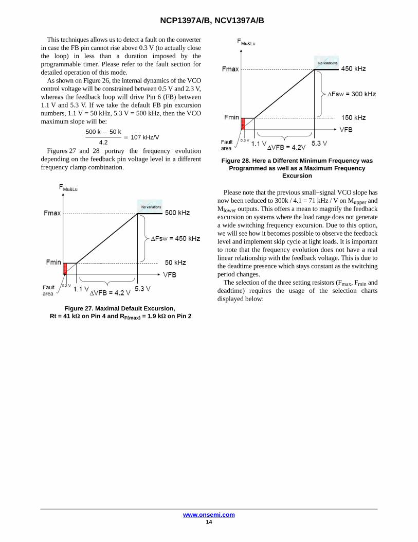
Figures 27 and 28 portray the frequency evolutiondepending on the feedback pin voltage level in a differentfrequency clamp combination.
Figure 27. Maximal Default Excursion, Rt = 41 k� on Pin 4 and RF(max) = 1.9 k� on Pin 2
Figure 28. Here a Different Minimum Frequency wasProgrammed as well as a Maximum Frequency
Excursion
Please note that the previous small−signal VCO slope hasnow been reduced to 300k / 4.1 = 71 kHz / V on Mupper andMlower outputs. This offers a mean to magnify the feedbackexcursion on systems where the load range does not generatea wide switching frequency excursion. Due to this option,we will see how it becomes possible to observe the feedbacklevel and implement skip cycle at light loads. It is importantto note that the frequency evolution does not have a reallinear relationship with the feedback voltage. This is due tothe deadtime presence which stays constant as the switchingperiod changes.
The selection of the three setting resistors (Fmax, Fmin anddeadtime) requires the usage of the selection chartsdisplayed below:

NCP1397A/B, NCV1397A/B
www.onsemi.com15
50
150
250
350
450
550
1.9 11.9 21.9 31.9 41.9
Figure 29. Maximum Switching Frequency ResistorSelection Depending on the Adopted Minimum
Switching Frequency
RFmax (k�)
Fm
ax (
kHz)
VCC = 15 VVFB = 6.5 VDT = 300 ns
Fmin = 200 kHz
Fmin = 50 kHz
100
150
200
250
300
350
400
450
500
2 4 6 8 10 12 14 16 18 20RFmin (k�)
Fm
in (
kHz)
20
30
40
50
60
70
80
90
100
20 30 40 50 60 70 80 90 100 110
Figure 30. Minimum Switching Frequency ResistorSelection (Fmin = 100 kHz to 500 kHz)
Figure 31. Minimum Switching Frequency ResistorSelection (Fmin = 20 kHz to 100 kHz)
RFmin (k�)
Fm
in (
kHz)
VCC = 15 VVFB = 1 V
DT = 300 ns
VCC = 15 VVFB = 1 V
DT = 300 ns
100
300
500
700
900
1100
1300
1500
1700
1900
3.5 13.5 23.5 33.5 43.5 53.5 63.5 73.5 83.5RDT (k�)
DT
(ns
)
Figure 32. Deadtime Resistor Selection
ORing capability and optocoupler connectionconfigurations
If for any particular reason, there is a need for a frequencyvariation linked to an event appearance (instead of abruptlystopping pulses), then the FB pin lends itself very well to theaddition of other sweeping loops. Several diodes can easilybe used perform the job in case of reaction to a fault eventor to regulate on the output current (CC operation).Figure 33 shows how to do it.
Figure 33. Thanks to the FB Configuration, LoopORing is Easy to Implement
VCC
FBIn1
In220 k
VCO
The VCO configuration used in this IC also offers an easyway to connect optocoupler (or pulldown bipolar) directlyto the Rt pin instead of FB pin (refer to Figures 34 and 35).The optocoupler is then configured as “common emitter”and the operating frequency is controlled by the current thatis taken out from the Rt pin – we have current controlleroscillator (CCO). If one uses this configuration it is neededto maintain FB pin voltage between 0.3 V and 1 V otherwisethe FB fault will be detected. The FB pin can be still used foropen FB loop detection in some applications – to do so it isneeded to keep optcoupler emitter voltage higher then 0.3 Vfor nominal load conditions. One needs to take RFBpulldown resistor into account when using thisconfiguration. It is possible to implement skip mode usingSkip/disable input and emitter resistors Rskip1 and Rskip2.

NCP1397A/B, NCV1397A/B
www.onsemi.com16
Figure 34. Feedback Configuration Using Direct Connection to the Rt Pin
SSFmax
Rt
FB
Skip/Disable
VCC
GND
NCP1397
Rskip2
Rskip1
Rc
OK1
RFstart
RFmin
CSS
Fstart(adj) − RFstart/RFminFmin(adj) − RFminFmax(adj) − Rc + Rskip1 + Rskip2
Figure 35. Feedback Configuration Using Direct Connection to the Rt Pin – No Open FB Loop Detection
SSFmax
Rt
FB
Skip/Disable
VCC
GND
NCP1397
Rskip2
Rskip1
Rc
OK1
RFstart
RFmin
CSS
Fstart(adj) − RFstart/RFminFmin(adj) − RFminFmax(adj) − Rc + Rskip1 + Rskip2
1N4148
Rbias
Dead−Time ControlDeadtime control is an absolute necessity when the
half−bridge configuration comes to play. The deadtimetechnique consists in inserting a period during which bothhigh and low side switches are off. Of course, the deadtimeamount differs depending on the switching frequency, hencethe ability to adjust it on this controller. The option rangesbetween 100 ns and 2 �s. The deadtime is actually made bycontrolling the oscillator discharge current. Figure 36portrays a simplified VCO circuit based on Figure 25.
During the discharge time, the clock comparator is high andinvalidates the AND gates: both outputs are low. When thecomparator goes back to the low level, during the timingcapacitor Ct recharge time, A and B outputs are validated.By connecting a resistor RDT to ground, it creates a currentwhose image serves to discharge the Ct capacitor: we controlthe dead−time. The typical range evolves between 100 ns(RDT = 3.5 k�) and 2 �s (RDT = 83.5 k�). Figure 39 showsthe typical waveforms.

NCP1397A/B, NCV1397A/B
www.onsemi.com17
Figure 36. Dead−time Generation
VDD
Icharge:FSW(min) + FSW(max)
Idis
Ct
RDT
DT
Vref
+ 3 V−1 V
−
+Clk
DS
Q
Q
R
A B
Soft−Start SequenceIn resonant controllers, a soft−start is needed to avoid
suddenly applying the full current into the resonating circuit.With this controller the soft−start duration is fully adjustableusing eternal components. The purpose of the Soft−Start pinis to discharge Soft−Start capacitor before IC restart and incase of fault conditions detected by Fault input.
Once the controller starts operation, the Soft−Startcapacitor (refer to Figure 37) is fully discharged and thus itstarts charging from the Rt pin. The charging currentincreases operating frequency of the controller above Fmin.As the soft−start capacitor charges, the frequency smoothlydecreases down to Fmin. Of course, practically, the feedbackloop is supposed to take over the VCO lead as soon as theoutput voltage has reached the target. If not, then theminimum switching frequency is reached and a fault isdetected on the feedback pin (typically below 300 mV).Figure 38 depicts a typical LLC startup using NCP1397A/Bcontroller.
Figure 37. Soft−Start Components Arrangement
SSFmax
Rt
GND
NCP1397
RF(start)
RFmin
RFmaxCSS
Fstart(adj) − RFstart/RFminFmin(adj) − RFminFmax(adj) − RFmax
Figure 38. A Typical Startup Sequence on a LLCConverter Using NCP1397
SS Action
Target isReached
Please note that the soft−start capacitor is discharged in thefollowing conditions:− A startup sequence− During auto−recovery burst mode− A brown−out recovery− A temperature shutdown recovery
The skip/disable input undergoes a special treatment.Since we want to implement skip cycle using this input, wecannot activate the soft−start every time the feedback pinstops the operations in low power mode. Therefore, whenthe skip/enable pin is released, no soft−start occurs to offerthe best skip cycle behavior. However, it is very possible tocombine skip cycle and true disable, e.g. via ORing diodesdriving Pin 8. In that case, if a signal maintains theskip/disable input high long enough to bring the feedbacklevel down (below 0.3 V) since the output voltage starts tofall down, then the soft−start discharge switch is activated.

NCP1397A/B, NCV1397A/B
www.onsemi.com18
0
1.00
2.00
3.00
4.00
0
4.00
8.00
12.0
16.0
time in seconds
−8.00
−4.00
0
4.00
8.00
Figure 39. Typical Oscillator Waveforms
Ct Voltage
56.2 � 65.9 � 75.7 � 85.4 � 95.1 �
Plo
t3D
iffer
ence
in V
olts
Plo
t2C
lock
in V
olts
Plo
t1V
ct in
Vol
ts
Clock PulsesDT
DTDT
A − B
Brown−Out protectionThe Brown−Out circuitry (BO) offers a way to protect the
resonant converter from low DC input voltages. Below agiven level, the controller blocks the output pulses, above it,it authorizes them. The internal circuitry, depicted byFigure 40, offers a way to observe the high−voltage (HV)rail. A resistive divider made of Rupper and Rlower, brings aportion of the HV rail on Pin 5. Below the turn−on level, the28 �A current source IBO is off. Therefore, the turn−onlevel solely depends on the division ratio brought by theresistive divider.
Figure 40. The Internal Brown−out Configuration withan Offset Current Source
VDD
+VBO
−
+
ON/OFFIBO
BO
Vbulk
Rupper
Rlower
BO

NCP1397A/B, NCV1397A/B
www.onsemi.com19
time in seconds
0
4.0
8.0
12.0
16.0
50
150
250
350
450
Figure 41. Simulation Results for 350 / 250 ON / OFF Levels
20 � 60 � 100 � 140 � 180 �
Vin
250 V
351 V
BO
Plo
t1 V
in in
Vol
ts
Vcm
p in
Vol
ts
To the contrary, when the internal BO signal is high(Mlower and Mupper pulse), the IBO source is activated andcreates a hysteresis. As a result, it becomes possible to selectthe turn−on and turn−off levels via a few lines of algebra:
IBO is off
V(�) � Vbulk1 �Rlower
Rlower � Rupper
(eq. 1)
IBO is on
V(�) � Vbulk2 �Rlower
Rlower � Rupper(eq. 2)
� IBO ��Rlower � Rupper
Rlower � Rupper�
We can now extract Rlower from Equation 1 and plug it intoEquation 2, then solve for Rupper:
Rupper � Rlower �Vbulk1 � VBO
VBO
Rlowerer � VBO �Vbulk1 � Vbulk2
IBO � �Vbulk1 � VBO�
If we decide to turn−on our converter for Vbulk1 equals350 V and turn it off for Vbulk2 equals 250 V, then we obtain:
Rupper = 3.57 M�
Rlower = 10.64 k�The bridge power dissipation is 4002 / 3.781 M� =
45 mW when front−end PFC stage delivers 400 V.
Figure 41 simulation result confirms our calculations.
Latchoff ProtectionThere are some situations where the converter shall be
fully turned−off and stay latched. This can happen inpresence of an overvoltage (the feedback loop is drifting) orwhen an over temperature is detected. Thanks to the additionof a comparator on the BO pin, a simple external circuit canlift up this pin above Vlatch (4 V typical) and permanentlydisable pulses. The VCC needs to be cycled down below6.5 V typically to reset the controller.

NCP1397A/B, NCV1397A/B
www.onsemi.com20
Figure 42. Adding a Comparator on the BO Pin Offers a way to Latch−off the Controller
−+
20 �sRC To permanent
latch
+Vlatch
VDD
−+
BO
+VBO
BO
Rlower
Rupper
VbulkVCC
Q1
NTC
Vout
IBO
On Figure 42, Q1 is blocked and does not bother the BOmeasurement as long as the NTC and the optocoupler are notactivated. As soon as the secondary optocoupler senses anOVP condition, or the NTC reacts to a high ambienttemperature, Q1 base is brought to ground and the BO pingoes up, permanently latching off the controller.
Protection CircuitryThis resonant controller offers a dedicated input (Fault
input) to detect primary overcurrent conditions and protectpower stage from damage.
Once the voltage on the Fault input exceeds 1.04 Vthreshold the external timer capacitor starts charging byItimer1 current. Simultaneously the Soft−Start dischargeswitch is activated to shift operating frequency up to keepprimary current at acceptable level. In case the overloaddisappears fast enough the Soft−Start discharge switch isopen, Itimer1 current turned−off and timer capacitor
discharges via an external parallel resistor. In case theoverload lasts for more than timer duration (given by Itimer,Vtimer, Ctimer and Rtimer) the IC stops the operation and waitsuntil the Ctimer will discharge to 1 V. The application thenrestarts via Soft−Start.
In case of heavy overload, like transformer short circuit,the primary current grows very fast and thus could reachdanger level prior the fault timer elapses. The NCP1397Btherefore features additional comparator (1.55 V) on theFault input to permanently latch the application and protectagainst destruction. Figure 44 depicts the architecture of thefault circuitry for NCP1397B controller.
The NCP1397A features second fault comparator as wellbut in this case it doesn’t latches off the IC but speeds up theFault timer capacitor charging by turning on additionalcurrent source Itimer2 – refer to Figure 43. The NCP1397Acan thus be used in applications that have to recoverautomatically from any fault conditions.

NCP1397A/B, NCV1397A/B
www.onsemi.com21
Figure 43. Fault Input Logic for NCP1397A
VDD
Itimer1
ResetUVLO
Rtimer
CtimerCtimer
+-
+Vref(fault)
+ -
+
VtimerONVtimerOFF
1 = ok0 = fault
+-
Vref(skip)
Skip/Disable
+
1 = ok0 = fault
DRIVINGLOGIC
SS
A A
B B
Reset
Fault
AverageInput
Current
To Primary
FB
Skip
VCC
FB
SS(dis) Css
discharge at VCC(on)/restart if VFB < 0.3 V
+-
+Vref(OCP)
VDD
Itimer2
Current SensingCircuitry

NCP1397A/B, NCV1397A/B
www.onsemi.com22
Figure 44. Fault Input Logic for NCP1397B
VDD
Itimer1
ResetUVLO
Rtimer
CtimerCtimer
+-
+Vref(fault)
+ -
+
VtimerONVtimerOFF
1 = ok0 = fault
+-
Vref(skip)
Skip/Disable
+
1 = ok0 = fault
DRIVINGLOGIC
SS
A A
B B
Reset
Fault
AverageInput
Current
To Primary
FB
Skip
VCC
FB
SS(dis) Css
discharge at VCC(on)/restart if VFB < 0.3 V
+-
+Vref(OCP)
Current SensingCircuitry
to latch
On Figures 43 and 44 examples, a voltage proportional toprimary current, once averaged, gives an image of the inputpower in case Vin is kept constant via a PFC circuit. If theoutput loading increases above a certain level, the voltage onthis pin will pass the 1 V threshold and start the timer. If the
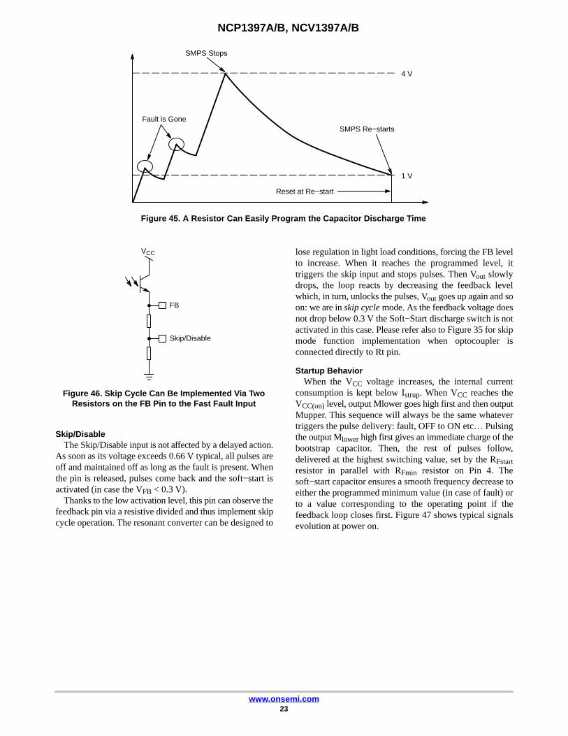
overload stays there, after a few tens of milli −seconds,switching pulses will disappear and a protectiveauto−recovery cycle will take place. Adjusting the resistorR in parallel with the timer capacitor will give the flexibilityto adjust the fault burst mode (refer to Figure 45).
NCP1397A/B, NCV1397A/B
www.onsemi.com23
Figure 45. A Resistor Can Easily Program the Capacitor Discharge Time
4 V
1 V
SMPS Re−starts
SMPS Stops
Reset at Re−start
Fault is Gone
Skip/Disable
FB
VCC
Figure 46. Skip Cycle Can Be Implemented Via TwoResistors on the FB Pin to the Fast Fault Input
Skip/DisableThe Skip/Disable input is not affected by a delayed action.
As soon as its voltage exceeds 0.66 V typical, all pulses areoff and maintained off as long as the fault is present. Whenthe pin is released, pulses come back and the soft−start isactivated (in case the VFB < 0.3 V).
Thanks to the low activation level, this pin can observe thefeedback pin via a resistive divided and thus implement skipcycle operation. The resonant converter can be designed to
lose regulation in light load conditions, forcing the FB levelto increase. When it reaches the programmed level, ittriggers the skip input and stops pulses. Then Vout slowlydrops, the loop reacts by decreasing the feedback levelwhich, in turn, unlocks the pulses, Vout goes up again and soon: we are in skip cycle mode. As the feedback voltage doesnot drop below 0.3 V the Soft−Start discharge switch is notactivated in this case. Please refer also to Figure 35 for skipmode function implementation when optocoupler isconnected directly to Rt pin.
Startup BehaviorWhen the VCC voltage increases, the internal current
consumption is kept below Istrup. When VCC reaches theVCC(on) level, output Mlower goes high first and then outputMupper. This sequence will always be the same whatevertriggers the pulse delivery: fault, OFF to ON etc… Pulsingthe output Mlower high first gives an immediate charge of thebootstrap capacitor. Then, the rest of pulses follow,delivered at the highest switching value, set by the RFstartresistor in parallel with RFmin resistor on Pin 4. Thesoft−start capacitor ensures a smooth frequency decrease toeither the programmed minimum value (in case of fault) orto a value corresponding to the operating point if thefeedback loop closes first. Figure 47 shows typical signalsevolution at power on.

NCP1397A/B, NCV1397A/B
www.onsemi.com24
Figure 47. At Power On, Output A is First Activated and the Frequency Slowly Decreases Based on the Soft−StartCapacitor Voltage
Figure 47 depicts an auto−recovery situation, where thetimer has triggered the end of output pulses. In that case, theVCC level was given by an auxiliary power supply, hence itsstability during the hiccup. A similar situation can arise if theuser selects a more traditional startup method, with anauxiliary winding. In that case, the VCC(min) comparator
stops the output pulses whenever it is activated, that is to say,when VCC falls below 9.5 V typical. At this time, the VCCpin still receives its bias current from the startup resistor andincreases toward VCC(on). When the voltage reachesVCC(on), a standard sequence takes place, involving asoft−start. Figure 48 portrays this behavior.

NCP1397A/B, NCV1397A/B
www.onsemi.com25
Figure 48. When the VCC is to Low, All Pulses are Stopped Until VCC Goes Back to the Startup Voltage
The High−Voltage DriverThe driver features a traditional bootstrap circuitry,
requiring an external high−voltage diode for the capacitorrefueling path. Figure 49 shows the internal architecture ofthe high−voltage section.
Figure 49. The Internal High−voltage Section of the NCP1397
+
Vboot
Mupper
HB
Cboot
Dboot
auxVCC
GND
VCC
Mlower
HV
UVLO
S
Q
Q
R
Delay
LevelShifter
PulseTrigger
Fault
A
B

NCP1397A/B, NCV1397A/B
www.onsemi.com26
The device incorporates an upper UVLO circuitry thatmakes sure enough Vgs is available for the upper sideMOSFET. The B and A outputs are delivered by the internallogic, as Figure 43 testifies. A delay is inserted in the lowerrail to ensure good matching between these propagatingsignals.
As stated in the maximum rating section, the floatingportion can go up to 600 VDC and makes the IC perfectlysuitable for offline applications featuring a 400 V PFCfront−end stage.
ORDERING INFORMATIONDevice Package Shipping†
NCP1397ADR2G
SOIC−16, Less Pin 13(Pb−Free) 2500 / Tape & Reel
NCV1397ADR2G*
NCP1397BDR2G
NCV1397BDR2G*
†For information on tape and reel specifications, including part orientation and tape sizes, please refer to our Tape and Reel PackagingSpecification Brochure, BRD8011/D.
*NCV Prefix for Automotive and Other Applications Requiring Unique Site and Control Change Requirements; AEC−Q100 Qualified and PPAPCapable.

SOIC−16 NB, LESS PIN 13CASE 751AM−01
ISSUE ODATE 20 AUG 2007SCALE 1:1
NOTES:1. DIMENSIONING AND TOLERANCING PER ASME
Y14.5M, 1994.2. CONTROLLING DIMENSION: MILLIMETERS.3. DIMENSION b DOES NOT INCLUDE DAMBAR
PROTRUSION. ALLOWABLE PROTRUSION SHALL BE0.13 TOTAL IN EXCESS OF THE b DIMENSION ATMAXIMUM MATERIAL CONDITION.
4. DIMENSIONS D AND E DO NOT INCLUDE MOLDPROTRUSIONS.
5. MAXIMUM MOLD PROTRUSION 0.15 PER SIDE.
1 8
16 9
SEATINGPLANE
L
M
h x 45�
e15X
H E
D
M0.25 B M
A1
A
DIM MIN MAXMILLIMETERS
D 9.80 10.00E 3.80 4.00
A 1.35 1.75
b 0.35 0.49
L 0.40 1.25
e 1.27 BSC
C 0.19 0.25
A1 0.10 0.25
M 0 7
H 5.80 6.20h 0.25 0.50
� �
6.40
15X0.58
15X 1.12
1.27
DIMENSIONS: MILLIMETERS
1
PITCH
SOLDERING FOOTPRINT
16
8 9
M0.25 A S
b 15X
T B S
A B
C
C
XXXXX = Specific Device CodeA = Assembly LocationWL = Wafer LotY = YearWW = Work WeekG = Pb−Free Package
GENERICMARKING DIAGRAM*
*This information is generic. Please referto device data sheet for actual partmarking. Pb−Free indicator, “G”, mayor not be present.
1
16
XXXXXXXXXGAWLYWW
MECHANICAL CASE OUTLINE
PACKAGE DIMENSIONS
ON Semiconductor and are trademarks of Semiconductor Components Industries, LLC dba ON Semiconductor or its subsidiaries in the United States and/or other countries.ON Semiconductor reserves the right to make changes without further notice to any products herein. ON Semiconductor makes no warranty, representation or guarantee regardingthe suitability of its products for any particular purpose, nor does ON Semiconductor assume any liability arising out of the application or use of any product or circuit, and specificallydisclaims any and all liability, including without limitation special, consequential or incidental damages. ON Semiconductor does not convey any license under its patent rights nor therights of others.
98AON25333DDOCUMENT NUMBER:
DESCRIPTION:
Electronic versions are uncontrolled except when accessed directly from the Document Repository.Printed versions are uncontrolled except when stamped “CONTROLLED COPY” in red.
PAGE 1 OF 1SOIC−16 NB, LESS PIN 13
© Semiconductor Components Industries, LLC, 2019 www.onsemi.com

onsemi, , and other names, marks, and brands are registered and/or common law trademarks of Semiconductor Components Industries, LLC dba “onsemi” or its affiliatesand/or subsidiaries in the United States and/or other countries. onsemi owns the rights to a number of patents, trademarks, copyrights, trade secrets, and other intellectual property.A listing of onsemi’s product/patent coverage may be accessed at www.onsemi.com/site/pdf/Patent−Marking.pdf. onsemi reserves the right to make changes at any time to anyproducts or information herein, without notice. The information herein is provided “as−is” and onsemi makes no warranty, representation or guarantee regarding the accuracy of theinformation, product features, availability, functionality, or suitability of its products for any particular purpose, nor does onsemi assume any liability arising out of the application or useof any product or circuit, and specifically disclaims any and all liability, including without limitation special, consequential or incidental damages. Buyer is responsible for its productsand applications using onsemi products, including compliance with all laws, regulations and safety requirements or standards, regardless of any support or applications informationprovided by onsemi. “Typical” parameters which may be provided in onsemi data sheets and/or specifications can and do vary in different applications and actual performance mayvary over time. All operating parameters, including “Typicals” must be validated for each customer application by customer’s technical experts. onsemi does not convey any licenseunder any of its intellectual property rights nor the rights of others. onsemi products are not designed, intended, or authorized for use as a critical component in life support systemsor any FDA Class 3 medical devices or medical devices with a same or similar classification in a foreign jurisdiction or any devices intended for implantation in the human body. ShouldBuyer purchase or use onsemi products for any such unintended or unauthorized application, Buyer shall indemnify and hold onsemi and its officers, employees, subsidiaries, affiliates,and distributors harmless against all claims, costs, damages, and expenses, and reasonable attorney fees arising out of, directly or indirectly, any claim of personal injury or deathassociated with such unintended or unauthorized use, even if such claim alleges that onsemi was negligent regarding the design or manufacture of the part. onsemi is an EqualOpportunity/Affirmative Action Employer. This literature is subject to all applicable copyright laws and is not for resale in any manner.
PUBLICATION ORDERING INFORMATIONTECHNICAL SUPPORTNorth American Technical Support:Voice Mail: 1 800−282−9855 Toll Free USA/CanadaPhone: 011 421 33 790 2910
LITERATURE FULFILLMENT:Email Requests to: [email protected]
onsemi Website: www.onsemi.com
Europe, Middle East and Africa Technical Support:Phone: 00421 33 790 2910For additional information, please contact your local Sales Representative
◊