ucc28600 8-pin quasi-resonant flyback green-mode
TRANSCRIPT
1
2
3
4
8
7
6
5
VCC
DRV
GND
ZCD
VO_SNS
COMP
MULTIN
CS
UCC28051
CBULK
1
2
3
4
8
7
6
5
STATUS
OVP
VDD
OUT
SS
FB
CS
GND
UCC28600CSS
CBP R
PL
RSU
RCS
CVDD
Primary Secondary
TL431
Feedback
ROVP2
ROVP1
18 V
CB
NP
NS
NB
M1
Product
Folder
Sample &Buy
Technical
Documents
Tools &
Software
Support &Community
ReferenceDesign
UCC28600SLUS646K –NOVEMBER 2005–REVISED AUGUST 2015
UCC28600 8-Pin Quasi-Resonant Flyback Green-Mode Controller1 Features 3 Description
The UCC28600 is a PWM controller with advanced1• Green-Mode Controller With Advanced Energy
energy features to meet stringent world-wide energySaving Featuresefficiency requirements.
• Quasi-Resonant Mode Operation for ReducedUCC28600 integrates built-in advanced energyEMI and Low Switching Losses (Low-Voltagesaving features with high-level protection features toValley Switching)provide cost-effective solutions for energy-efficient• Low Standby Current for Minimum System No- power supplies. UCC28600 incorporates frequency
Load Power Consumption fold-back and green-mode operation to reduce the• Low Start-up Current: 25-μA Maximum switching losses at light-load and no-load conditions.• Programmable Line and Load Over-Voltage UCC28600 is available in the 8-pin SOIC package.
Protection Operating junction temperature range is –40°C to+105°C.• Internal Over-Temperature Protection
• Current Limit Protection The UCC28600 Design Calculator, (SLVC104),located in the Tools and Software section of the– Cycle-by-Cycle Power LimitUCC28600 product folder, provides a user-interactive– Primary-Side Over-Current Hiccup Restart iterative process for selecting recommendedMode component values for an optimal design.
• 1-A Sink, –0.75-A Source TrueDrive™ Gate DriveOutput Device Information (1)
PART NUMBER PACKAGE BODY SIZE (NOM)• Programmable Soft-StartUCC28600 SOIC (8) 4.90 mm × 3.91 mm• Green-Mode Status Pin (PFC Disable Function)(1) For all available packages, see the orderable addendum at
the end of the data sheet.2 Applications• Bias Supplies for LCD-Monitors, LCD-TV, PDP-
TV, and Set Top Boxes• AC-to-DC Adapters and Off-Line Battery Chargers• Energy Efficient Power Supplies up to 200 W
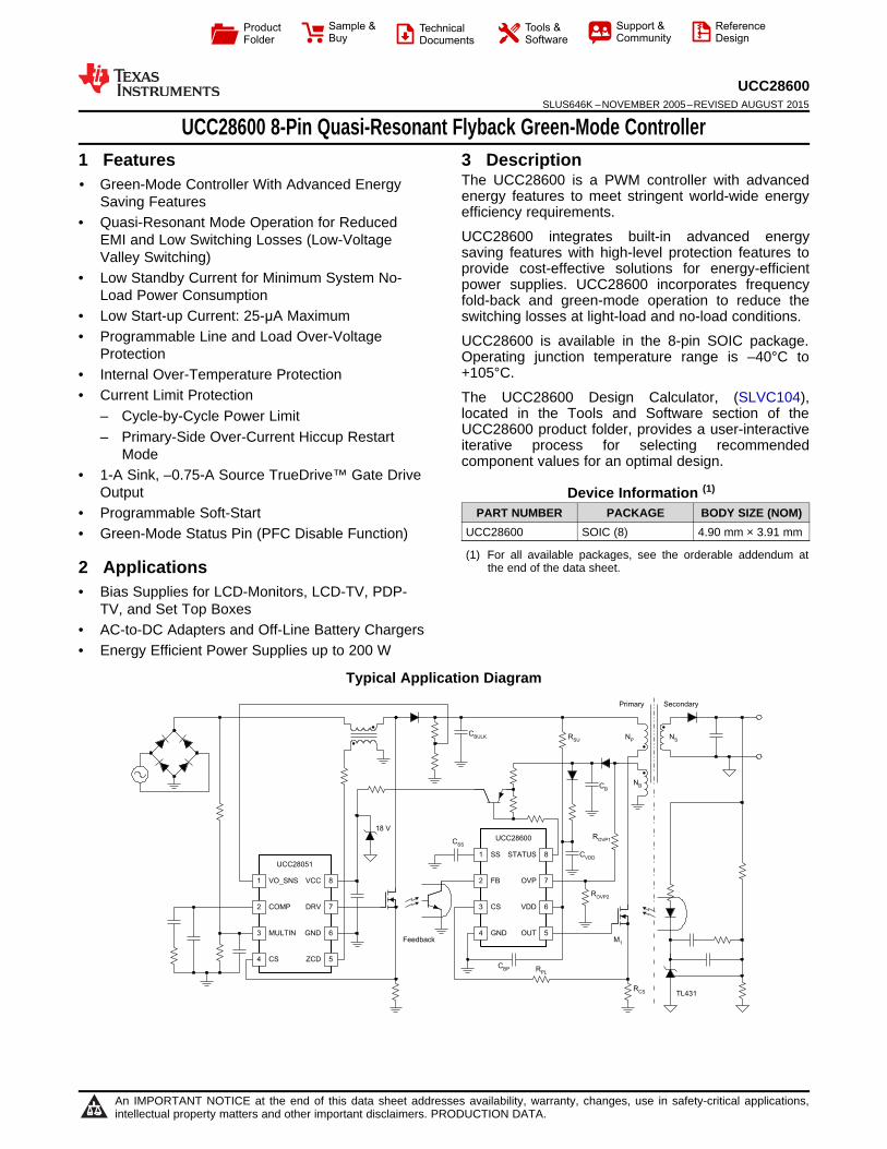
Typical Application Diagram
1
An IMPORTANT NOTICE at the end of this data sheet addresses availability, warranty, changes, use in safety-critical applications,intellectual property matters and other important disclaimers. PRODUCTION DATA.
UCC28600SLUS646K –NOVEMBER 2005–REVISED AUGUST 2015 www.ti.com
Table of Contents7.4 Device Functional Modes........................................ 181 Features .................................................................. 1
8 Application and Implementation ........................ 212 Applications ........................................................... 18.1 Application Information............................................ 213 Description ............................................................. 18.2 Typical Application ................................................. 214 Revision History..................................................... 28.3 Do's and Don'ts ...................................................... 335 Pin Configuration and Functions ......................... 3
9 Power Supply Recommendations ...................... 346 Specifications......................................................... 410 Layout................................................................... 346.1 Absolute Maximum Ratings ...................................... 4
10.1 Layout Guidelines ................................................. 346.2 ESD Ratings ............................................................ 410.2 Layout Example .................................................... 356.3 Recommended Operating Conditions....................... 4
11 Device and Documentation Support ................. 366.4 Thermal Information .................................................. 411.1 Device Support .................................................... 366.5 Electrical Characteristics........................................... 511.2 Documentation Support ....................................... 366.6 Timing Requirements ................................................ 611.3 Trademarks ........................................................... 366.7 Typical Characteristics .............................................. 711.4 Electrostatic Discharge Caution............................ 367 Detailed Description .............................................. 811.5 Glossary ................................................................ 367.1 Overview ................................................................... 8
12 Mechanical, Packaging, and Orderable7.2 Functional Block Diagram ......................................... 8Information ........................................................... 377.3 Feature Description................................................. 11
4 Revision HistoryNOTE: Page numbers for previous revisions may differ from page numbers in the current version.
Changes from Revision J (July 2011) to Revision K Page
• Added Pin Configuration and Functions section, ESD table, Feature Description section, Device Functional Modes,Application and Implementation section, Power Supply Recommendations section, Layout section, Device andDocumentation Support section, and Mechanical, Packaging, and Orderable Information section. .................................... 1
• Changed Functional Block diagram........................................................................................................................................ 8• Changed Control Flow Chart diagram.................................................................................................................................. 11• Changed QR Detect Details image. ..................................................................................................................................... 13• Changed Oscillator Details image. ....................................................................................................................................... 14• Changed Fault Logic Details image...................................................................................................................................... 16• Changed Mode Control with FB Pin Voltage image. ........................................................................................................... 18• Changed Operation Mode Switching Frequencies image. .................................................................................................. 19
Changes from Revision H (November 2005) to Revision I Page
• Changed Equation 35 .......................................................................................................................................................... 29
2 Submit Documentation Feedback Copyright © 2005–2015, Texas Instruments Incorporated
Product Folder Links: UCC28600

1234
8765
SSFBCS
GND
STATUSOVPVDDOUT
UCC28600www.ti.com SLUS646K –NOVEMBER 2005–REVISED AUGUST 2015
5 Pin Configuration and Functions
D Package8-Pin SOICTop View
Pin FunctionsPIN
I/O DESCRIPTIONNAME NO.
Current sense input. Also programs power limit, and used to control modulation and activateovercurrent protection. The CS voltage input originates across a current sense resistor andCS 3 I ground. Power limit is programmed with an effective series resistance between this pin andthe current sense resistor.Feedback input or control input from the optocoupler to the PWM comparator used to controlthe peak current in the power MOSFET. An internal 20-kΩ resistor is between this pin andthe internal 5-V regulated voltage. Connect the collector of the photo-transistor of theFB 2 I feedback optocoupler directly to this pin; connect the emitter of the photo-transistor to GND.The voltage of this pin controls the mode of operation in one of the three modes: quasiresonant (QR), frequency foldback mode (FFM) and green mode (GM).Ground for internal circuitry. Connect a ceramic 0.1-μF bypass capacitor between VDD andGND 4 – GND, with the capacitor as close to these two pins as possible.1-A sink (TrueDrive™ ) and 0.75-A source gate drive output. This output drives the power
OUT 5 O MOSFET and switches between GND and the lower of VDD or the 13-V internal outputclamp.Over voltage protection (OVP) input senses line-OVP, load-OVP and the resonant trough for
OVP 7 I QR turn-on. Detect line, load and resonant conditions using the primary bias winding of thetransformer, adjust sensitivity with resistors connected to this pin.Soft-start programming pin. Program the soft-start rate with a capacitor to ground; the rate isdetermined by the capacitance and the internal soft-start charge current. The soft-startcapacitor should be placed as close as possible to the SS pin and GND, keeping traceSS 1 I length to a minimum. All faults discharge the SS pin to GND through an internal MOSFETwith an RDS(on) of approximately 100 Ω. The internal modulator comparator reacts to thelowest of the SS voltage, the internal FB voltage and the peak current limit.ACTIVE HIGH open drain signal that indicates the device has entered standby mode. This
STATUS 8 O pin can be used to disable the PFC control circuit (high impedance = green mode). STATUSpin is high during UVLO, (VDD < start-up threshold), and softstart, (SS < FB).Provides power to the device. Use a ceramic 0.1-μF by-pass capacitor for high-frequencyfiltering of the VDD pin, as described in the GND pin description. Operating energy is usuallyVDD 6 I delivered from auxiliary winding. To prevent hiccup operation during start-up, a larger energystorage cap is also needed between VDD and GND.
Copyright © 2005–2015, Texas Instruments Incorporated Submit Documentation Feedback 3
Product Folder Links: UCC28600
UCC28600SLUS646K –NOVEMBER 2005–REVISED AUGUST 2015 www.ti.com
6 Specifications
6.1 Absolute Maximum Ratingsover operating free-air temperature range (unless otherwise noted) (1)
MIN MAX UNITVDD Supply voltage range, IDD < 20 mA 32 VIDD Supply current 20 mAIOUT(sink) Output sink current (peak) 1.2 AIOUT(source) Output source current (peak) –0.8 A
Analog inputs: FB, CS, SS –0.3 6.0 VVOVP –1.0 6.0 VIOVP(source) –1.0 mAVSTATUS VDD = 0 V to 30 V 30 V
Power dissipation, SOIC-8 package, TA = 25°C 650 mWTLEAD Lead temperature 1,6 mm (1/16 inch) from case for 10 seconds 300 °CTJ Operating junction temperature –55 150 °CTstg Storage temperature –65 150 °C
(1) Stresses beyond those listed under Absolute Maximum Ratings may cause permanent damage to the device. These are stress ratingsonly, which do not imply functional operation of the device at these or any other conditions beyond those indicated under RecommendedOperating Conditions. Exposure to absolute-maximum-rated conditions for extended periods may affect device reliability.
6.2 ESD RatingsVALUE UNIT
Human body model (HBM), per ANSI/ESDA/JEDEC JS-001, all ±2000 Vpins (1)V(ESD) Electrostatic discharge
Charged device model (CDM), per JEDEC specification ±1500 VJESD22-C101, all pins (2)
(1) JEDEC document JEP155 states that 500-V HBM allows safe manufacturing with a standard ESD control process.(2) JEDEC document JEP157 states that 250-V CDM allows safe manufacturing with a standard ESD control process.
6.3 Recommended Operating Conditionsover operating free-air temperature range (unless otherwise noted)
MIN NOM MAX UNITVDD Input voltage 21 VCVDD VDD bypass capacitor 0.1 1.0 μFCFB FB filter capacitor 390 pFTJ Operating junction temperature –40 105 °C
6.4 Thermal InformationUCC28600
THERMAL METRIC (1) D (SOIC) UNIT8 PINS
RθJA Junction-to-ambient thermal resistance 108.9 °C/WRθJC(top) Junction-to-case (top) thermal resistance 55.5 °C/WRθJB Junction-to-board thermal resistance 48.9 °C/WψJT Junction-to-top characterization parameter 10.5 °C/WψJB Junction-to-board characterization parameter 48.5 °C/W
(1) For more information about traditional and new thermal metrics, see the Semiconductor and IC Package Thermal Metrics applicationreport, SPRA953.
4 Submit Documentation Feedback Copyright © 2005–2015, Texas Instruments Incorporated
Product Folder Links: UCC28600
UCC28600www.ti.com SLUS646K –NOVEMBER 2005–REVISED AUGUST 2015
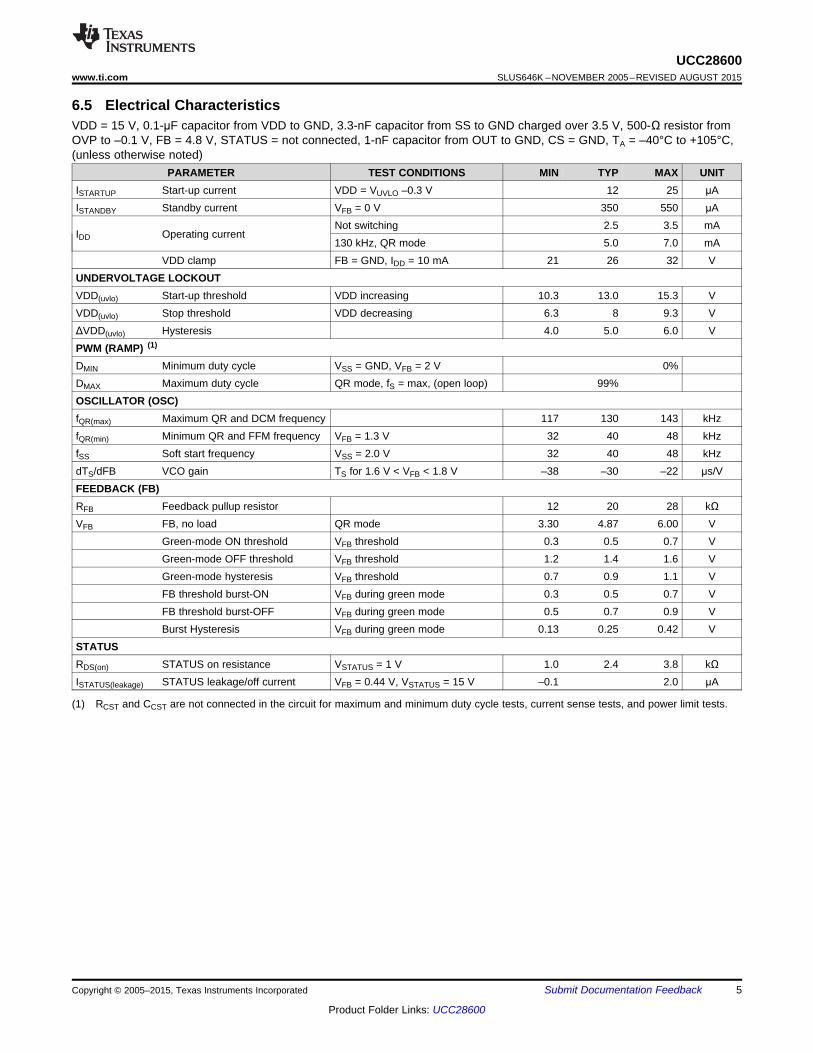
6.5 Electrical CharacteristicsVDD = 15 V, 0.1-μF capacitor from VDD to GND, 3.3-nF capacitor from SS to GND charged over 3.5 V, 500-Ω resistor fromOVP to –0.1 V, FB = 4.8 V, STATUS = not connected, 1-nF capacitor from OUT to GND, CS = GND, TA = –40°C to +105°C,(unless otherwise noted)
PARAMETER TEST CONDITIONS MIN TYP MAX UNITISTARTUP Start-up current VDD = VUVLO –0.3 V 12 25 μAISTANDBY Standby current VFB = 0 V 350 550 μA
Not switching 2.5 3.5 mAIDD Operating current
130 kHz, QR mode 5.0 7.0 mAVDD clamp FB = GND, IDD = 10 mA 21 26 32 V
UNDERVOLTAGE LOCKOUTVDD(uvlo) Start-up threshold VDD increasing 10.3 13.0 15.3 VVDD(uvlo) Stop threshold VDD decreasing 6.3 8 9.3 VΔVDD(uvlo) Hysteresis 4.0 5.0 6.0 VPWM (RAMP) (1)
DMIN Minimum duty cycle VSS = GND, VFB = 2 V 0%DMAX Maximum duty cycle QR mode, fS = max, (open loop) 99%OSCILLATOR (OSC)fQR(max) Maximum QR and DCM frequency 117 130 143 kHzfQR(min) Minimum QR and FFM frequency VFB = 1.3 V 32 40 48 kHzfSS Soft start frequency VSS = 2.0 V 32 40 48 kHzdTS/dFB VCO gain TS for 1.6 V < VFB < 1.8 V –38 –30 –22 μs/VFEEDBACK (FB)RFB Feedback pullup resistor 12 20 28 kΩVFB FB, no load QR mode 3.30 4.87 6.00 V
Green-mode ON threshold VFB threshold 0.3 0.5 0.7 VGreen-mode OFF threshold VFB threshold 1.2 1.4 1.6 VGreen-mode hysteresis VFB threshold 0.7 0.9 1.1 VFB threshold burst-ON VFB during green mode 0.3 0.5 0.7 VFB threshold burst-OFF VFB during green mode 0.5 0.7 0.9 VBurst Hysteresis VFB during green mode 0.13 0.25 0.42 V
STATUSRDS(on) STATUS on resistance VSTATUS = 1 V 1.0 2.4 3.8 kΩISTATUS(leakage) STATUS leakage/off current VFB = 0.44 V, VSTATUS = 15 V –0.1 2.0 μA
(1) RCST and CCST are not connected in the circuit for maximum and minimum duty cycle tests, current sense tests, and power limit tests.
Copyright © 2005–2015, Texas Instruments Incorporated Submit Documentation Feedback 5
Product Folder Links: UCC28600
UCC28600SLUS646K –NOVEMBER 2005–REVISED AUGUST 2015 www.ti.com
Electrical Characteristics (continued)VDD = 15 V, 0.1-μF capacitor from VDD to GND, 3.3-nF capacitor from SS to GND charged over 3.5 V, 500-Ω resistor fromOVP to –0.1 V, FB = 4.8 V, STATUS = not connected, 1-nF capacitor from OUT to GND, CS = GND, TA = –40°C to +105°C,(unless otherwise noted)
PARAMETER TEST CONDITIONS MIN TYP MAX UNITCURRENT SENSE (CS) (1)
ACS(FB) Gain = ΔVFB / ΔVCS QR mode 2.5 V/VShutdown threshold VFB = 2.4 V, VSS = 0 V 1.13 1.25 1.38 VCS discharge impedance CS = 0.1 V, VSS = 0 V 25 115 250 Ω
VCS(os) CS offset SS mode, VSS ≤ 2.0 V 0.35 0.40 0.45 VPOWER LIMIT (PL) (1)
IPL(cs) CS current OVP = –300 μA –165 –150 –135 μAPeak CS voltage QR mode 0.70 0.81 0.92 V
VPL PL threshold Peak CS voltage + CS offset 1.05 1.20 1.37 VSOFT START (SS)ISS(chg) Softstart charge current VSS = GND –8.3 –6.0 –4.5 μAISS(dis) Softstart discharge current VSS = 0.5 V 2.0 5.0 10 mAVSS Switching ON threshold Output switching start 0.8 1.0 1.2 VOVERVOLTAGE PROTECTION (OVP)IOVP(line) Line overvoltage protection IOVP threshold, OUT = HI –512 –450 –370 μA
VFB = 4.8 V, VSS = 5.0 V,VOVP(on) OVP voltage at OUT = HIGH –125 –25 mVIOVP(on), = –300 μAVOVP(load) Load overvoltage protection VOVP threshold, OUT = LO 3.37 3.75 4.13 VTHERMAL PROTECTION (TSP)
Thermal shutdown (TSP) 130 140 150 °Ctemperature (2)
Thermal shutdown hysteresis 15 °C
(2) Ensured by design. Not production tested.
6.6 Timing RequirementsMIN NOM MAX UNIT
CURRENT SENSE (CS) (1)
CS to output delay time (power limit), CS = 1.0 VPULSE 100 175 300 nsCS to output delay time (over current fault), CS = 1.45 VPULSE 50 100 150 ns
OUTtRISE Rise time, 10% to 90% of 13-V typical OUT clamp 50 75 nstFALL Fall time 10 20 ns
(1) RCST and CCST are not connected in the circuit for maximum and minimum duty cycle tests, current sense tests, and power limit tests.
6 Submit Documentation Feedback Copyright © 2005–2015, Texas Instruments Incorporated
Product Folder Links: UCC28600
-50 0 100 150
TJ - Temperature - °C
-512
-492
-472
-432
50
-412
-372
I OV
P O
ve
r-V
olt
ag
e P
rote
ctio
n T
hre
sho
ld -
PA
-452
-392
–50 0 100 150
T – Temperature – °CJ
0.70
0.75
0.80
0.85
50
0.90
0.95
PL
Th
resh
old
, Q
R M
od
e,
Peak C
S V
olt
ag
e –
V
–50 0 100 150
T – Temperature – °CJ
21
23
25
27
50
29
31
VD
D –
Cla
mp
Vo
ltag
e –
V
–50 0 100 150
T – Temperature – °CJ
117
122
127
132
50
137
142
f –
Sw
itch
ing
Fre
qu
en
cy –
kH
zS
UCC28600www.ti.com SLUS646K –NOVEMBER 2005–REVISED AUGUST 2015
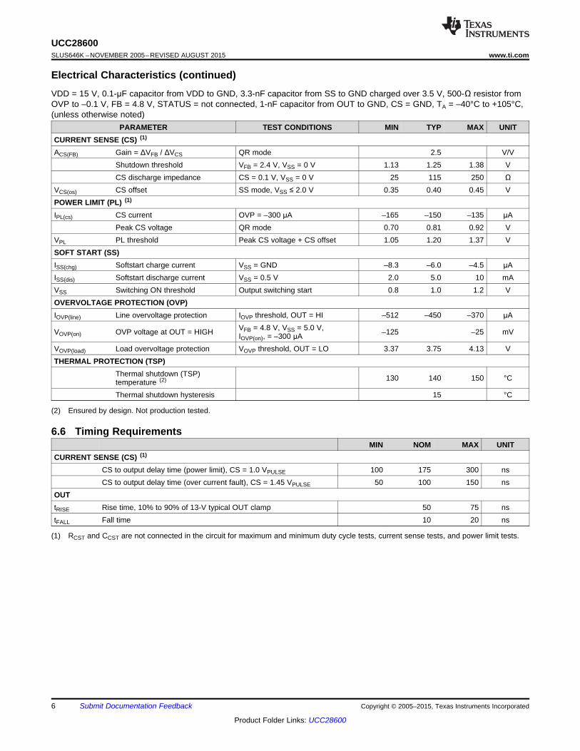
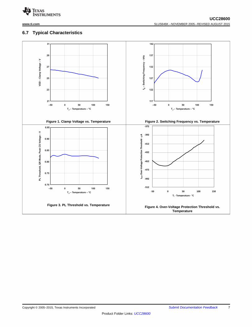
6.7 Typical Characteristics
Figure 1. Clamp Voltage vs. Temperature Figure 2. Switching Frequency vs. Temperature
Figure 3. PL Threshold vs. Temperature Figure 4. Over-Voltage Protection Threshold vs.Temperature
Copyright © 2005–2015, Texas Instruments Incorporated Submit Documentation Feedback 7
Product Folder Links: UCC28600
2
1
6
5.0 VREF
SS
VDD
4GND
5OUT
FB
1.5R
8
3
CS
VDD_OK +
CBULK
Feedback20 k:
CSS
7
OVP
On-Chip Thermal
Shutdown
REF
26 V
R
STATUS
13/8 V
RCS
ROVP1
ROVP2
CVDD
+
400 mV
REF
RSU
+ Q
QSET
CLR
D
REF
GAIN = 1/2.5
+
Modulation Comparison
UCC28600
Fault Logic
LINE_OVPLOAD_OVP
REF_OK
RUN
VDD_OK
CS
OVR_TSTATUSSS_DIS
GREEN MODE
FB_CLAMP
OSC_CLFB
QR DETECTLOAD_OVPLINE_OVP
QR_DONE
____OUT
CS
OSCILLATOR
QR_DONECLK
RUNSS_MODE
OSC_CL
RPL
PL1.2 V
SS_MODE BURST BURST
RVDD
VDD
ILINE
ILINE
2
VCS(os)
VREF
6PA
UCC28600SLUS646K –NOVEMBER 2005–REVISED AUGUST 2015 www.ti.com
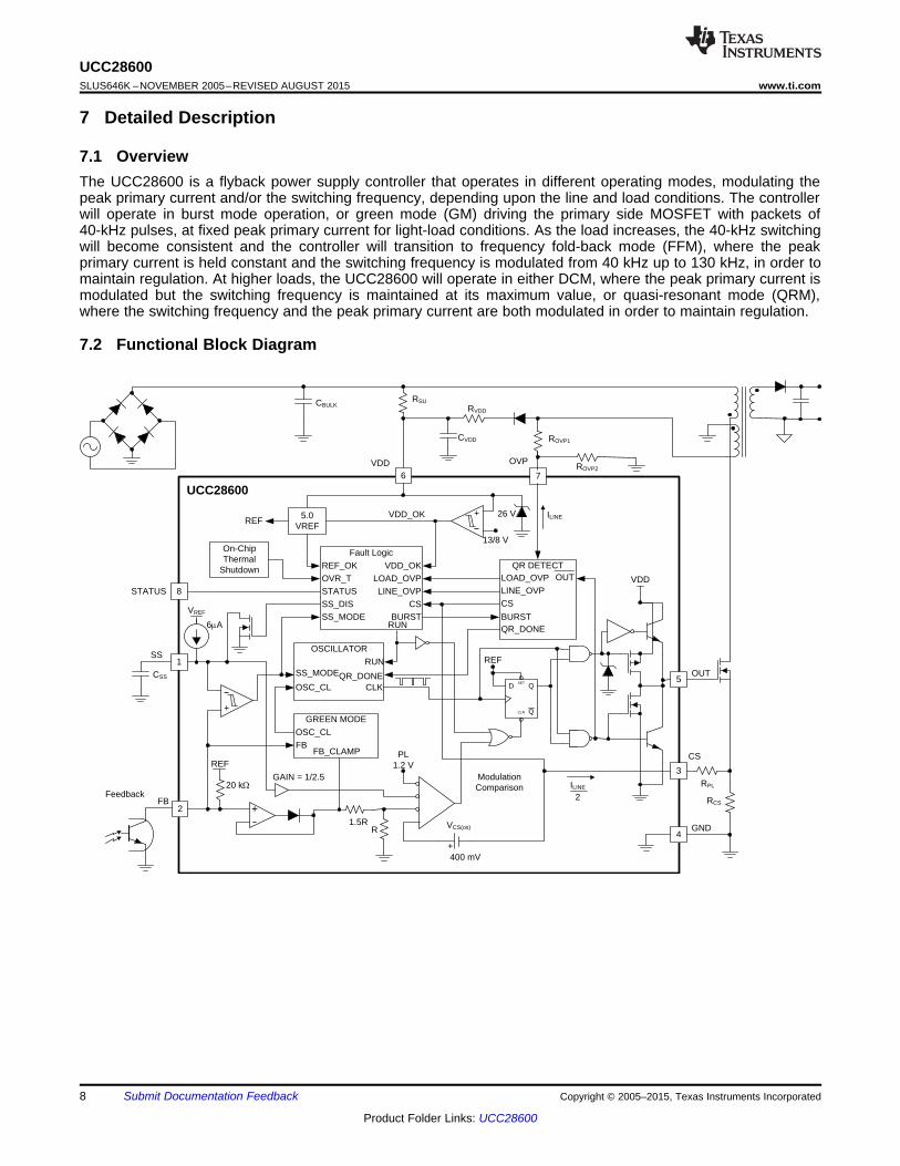
7 Detailed Description
7.1 OverviewThe UCC28600 is a flyback power supply controller that operates in different operating modes, modulating thepeak primary current and/or the switching frequency, depending upon the line and load conditions. The controllerwill operate in burst mode operation, or green mode (GM) driving the primary side MOSFET with packets of40-kHz pulses, at fixed peak primary current for light-load conditions. As the load increases, the 40-kHz switchingwill become consistent and the controller will transition to frequency fold-back mode (FFM), where the peakprimary current is held constant and the switching frequency is modulated from 40 kHz up to 130 kHz, in order tomaintain regulation. At higher loads, the UCC28600 will operate in either DCM, where the peak primary current ismodulated but the switching frequency is maintained at its maximum value, or quasi-resonant mode (QRM),where the switching frequency and the peak primary current are both modulated in order to maintain regulation.
7.2 Functional Block Diagram
8 Submit Documentation Feedback Copyright © 2005–2015, Texas Instruments Incorporated
Product Folder Links: UCC28600
2OUT OUT
SS(min)LIM
C Vt
2P
ª º « »« »¬ ¼
LOAD(ss) OUT OUT OUT(step)SS(min)
LOAD(ss) OUT(max)limit
R C V Vt n
2 R P
ª º ' « »« »¬ ¼
l
SS(min)
SS SSCS(FB) PL CS(os)
t duepower limitC I
A V V! u
u
OVP(line)
OVP2 OVP1B
OUT(shutdown) F OVP(load)P
VR R
NV V V
N
§ ·¨ ¸¨ ¸ ¨ ¸ ¨ ¸© ¹
BOVP1 BULK(ov)
OVP(line) P
N1R V
I N
§ · ¨ ¸
© ¹
PL CS(os) P(2) P(1)PL
CS(1) P(2) CS(2) P(1)
V V I IR
I I I I
PL CS(os) CS(2) CS(1)CS
CS(2) P(1) CS(1) P(2)
V V I IR
I I I I
UCC28600www.ti.com SLUS646K –NOVEMBER 2005–REVISED AUGUST 2015
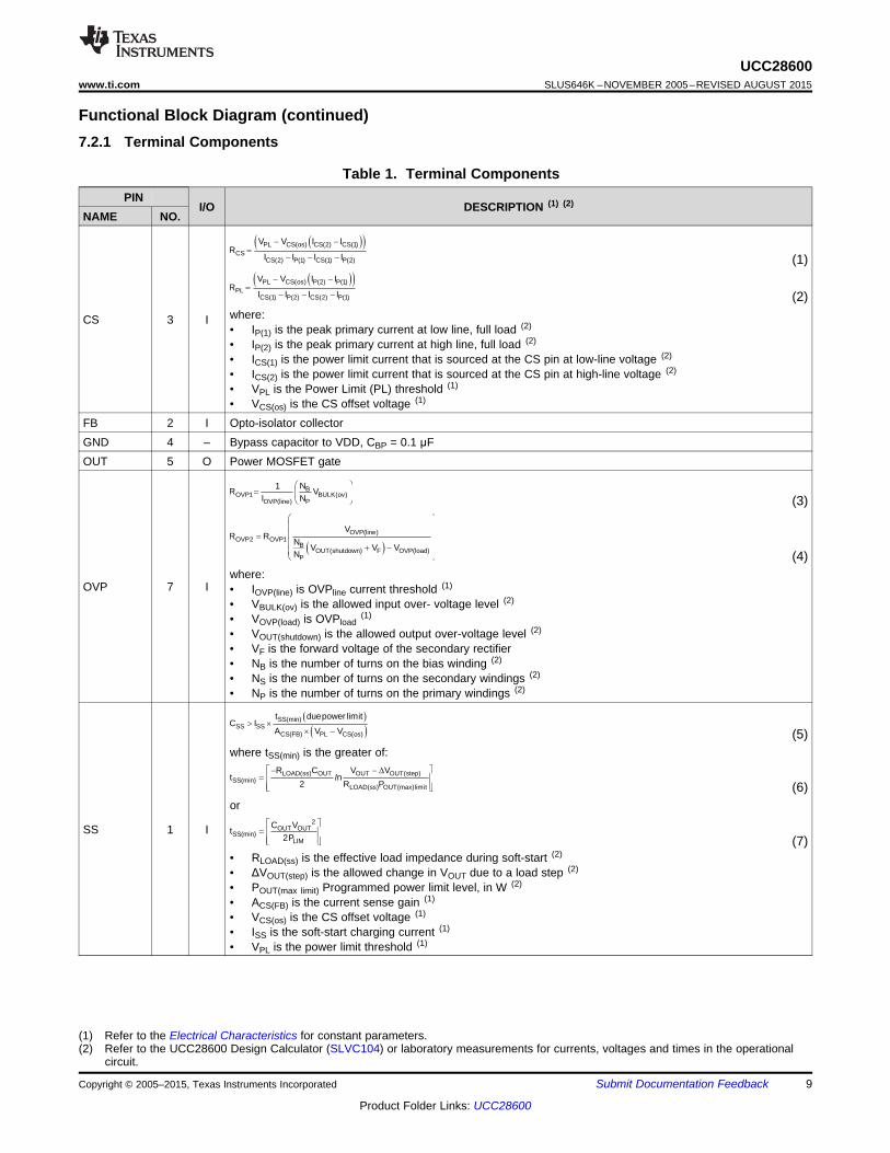
Functional Block Diagram (continued)7.2.1 Terminal Components
Table 1. Terminal ComponentsPIN
I/O DESCRIPTION (1) (2)NAME NO.
(1)
(2)where:CS 3 I• IP(1) is the peak primary current at low line, full load (2)
• IP(2) is the peak primary current at high line, full load (2)
• ICS(1) is the power limit current that is sourced at the CS pin at low-line voltage (2)
• ICS(2) is the power limit current that is sourced at the CS pin at high-line voltage (2)
• VPL is the Power Limit (PL) threshold (1)
• VCS(os) is the CS offset voltage (1)
FB 2 I Opto-isolator collectorGND 4 – Bypass capacitor to VDD, CBP = 0.1 μFOUT 5 O Power MOSFET gate
(3)
(4)where:
OVP 7 I • IOVP(line) is OVPline current threshold (1)
• VBULK(ov) is the allowed input over- voltage level (2)
• VOVP(load) is OVPload(1)
• VOUT(shutdown) is the allowed output over-voltage level (2)
• VF is the forward voltage of the secondary rectifier• NB is the number of turns on the bias winding (2)
• NS is the number of turns on the secondary windings (2)
• NP is the number of turns on the primary windings (2)
(5)where tSS(min) is the greater of:
(6)or
SS 1 I(7)
• RLOAD(ss) is the effective load impedance during soft-start (2)
• ΔVOUT(step) is the allowed change in VOUT due to a load step (2)
• POUT(max limit) Programmed power limit level, in W (2)
• ACS(FB) is the current sense gain (1)
• VCS(os) is the CS offset voltage (1)
• ISS is the soft-start charging current (1)
• VPL is the power limit threshold (1)
(1) Refer to the Electrical Characteristics for constant parameters.(2) Refer to the UCC28600 Design Calculator (SLVC104) or laboratory measurements for currents, voltages and times in the operational
circuit.
Copyright © 2005–2015, Texas Instruments Incorporated Submit Documentation Feedback 9
Product Folder Links: UCC28600

BULK(min)SU
STARTUP
VR
I
DS1(os) QR(max) LEAKAGE D SNUBBVDD
P ISS OUT(hi) QR(max)
V f L C CNR
4 N IDD C V f
§ ·§ ·S§ · ¨ ¸ ¨ ¸¨ ¸ ¨ ¸© ¹© ¹© ¹
SSVDD DD ISS OUT(hi) QR(max)
DD(uvlo)
TC I C V f
V
ª º « »
'« »¬ ¼
BURSTVDD DD ISS OUT(hi) QR(max)
DD(burst)
TC I C V f
V
ª º « »
'« »¬ ¼
CCST2 (uvlo on) BE(sat) DS(on) DS(on) BE(sat)
satST1
CCST2 BE(sat)
sat
IR VDD V R R V
RI
R V
ª º§ ·u u « »¨ ¸E« »© ¹¬ ¼
§ ·§ ·u ¨ ¸¨ ¸¨ ¸E© ¹© ¹
BE(off)ST2
STATUS(leakage)
VR
I
UCC28600SLUS646K –NOVEMBER 2005–REVISED AUGUST 2015 www.ti.com
Functional Block Diagram (continued)Table 1. Terminal Components (continued)
PINI/O DESCRIPTION (1) (2)
NAME NO.
(8)
(9)where:STATUS 8 O• βSAT is the gain of transistor QST in saturation• VBE(sat) is the base-emitter voltage of transistor QST in saturation• VDD(uvlo-on) is the start-up threshold (1)
• ICC is the collector current of QST• ISTATUS(leakage) is the maximum leakage/off current of the STATUS pin (1)
• VBE(off) is the maximum allowable voltage across the base emitter junction that will not turn QST on• RDS(on) is the RDS(on) of STATUS (1)
CVDD is the greater of:
(10)or
(11)
(12)
(13)where:VDD 6 I• IDD is the operating current of the UCC28600 (1)
• CISS is the input capacitance of MOSFET M1• VOUT(hi) is VOH of the OUT pin, either 13 V (typ) VOUT clamp or less as measured• fQR(max) is fS at high line, maximum load (1)
• TBURST is the measured burst mode period• ΔVDD(burst) is the allowed VDD ripple during burst mode• ΔVDD(uvlo) is the UVLO hysteresis (1)
• VDS1(os) is the amount of drain-source overshoot voltage• LLEAKAGE is the leakage inductance of the primary winding• CD is the total drain node capacitance of MOSFET M1• ISTARTUP is IDD start-up current of the UCC28600 (1)
• CSNUB is the snubber capacitor value• tSS is the soft start charge time (2)
10 Submit Documentation Feedback Copyright © 2005–2015, Texas Instruments Incorporated
Product Folder Links: UCC28600

START
VCC > 13 V?
Soft Start
Monitor VFB
2.0 V < VFB1.4 V < VFB < 2.0 VVFB < 1.4 V
Fixed V-secFreq. Foldback
(Light Load)
Quasi-Resonant Mode or DCM(Normal Load)
VFB < 0.5 V
VCC < 8 V?REF < 4 V?OVP = 1?OT = 1?OC = 1?
RUN = 1STATUS = 1
Y
N
Y
Y
RUN = 0STATUS = 1
Fixed V-sec40 kHz Burst
RUN = 0
N
N
Fixed V-sec40 kHz
Zero Pulses
STATUS = 1(In Green-Mode)
VFB > 0.5 VVFB > 0.7 V
STATUS = 0(In Run-Mode)
STATUS = 0(In Run-Mode)
STATUS = 0(In Run-Mode)
N
N
YYVFB > 1.4 V
N
Y
UCC28600www.ti.com SLUS646K –NOVEMBER 2005–REVISED AUGUST 2015
7.3 Feature DescriptionThe UCC28600 is a multi-mode controller, as illustrated in Figure 5 and Figure 12. The mode of operationdepends upon line and load conditions. Under all modes of operation, the UCC28600 terminates the OUT = HIsignal based on the switch current. Thus, the UCC28600 always operates in current mode control so that thepower MOSFET current is always limited.
Under normal operating conditions, the FB pin commands the operating mode of the UCC28600 at the voltagethresholds shown in the control flow chart, Figure 11. Soft-start and fault responses are the exception. Duringsoft start, the converter switching frequency is fixed at 40 kHz and FB is set to 5V. The soft-start mode islatched-OFF when VSS becomes greater than VFB for the first time after UVLOON. The soft-start state cannot berecovered until after passing UVLOOFF, and then, UVLOON.
From 100% to approximately 30% full rated power the UCC28600 controls the converter in quasi-resonant mode(QRM) or discontinuous conduction mode (DCM), where DCM operation is at the clamped maximum switchingfrequency (130 kHz). For loads that are between approximately 30% and 10% full rated power, the converteroperates in frequency foldback mode (FFM), where the peak switch current is constant and the output voltage isregulated by modulating the switching frequency for a given and fixed VIN. Effectively, operation in FFM results inthe application of constant volt-seconds to the flyback transformer each switching cycle. Voltage regulation inFFM is achieved by varying the switching frequency in the range from 130 kHz to 40 kHz. For extremely lightloads (below approximately 10% full rated power), the converter is controlled using bursts of 40-kHz pulses.
Figure 5. Control Flow Chart
Copyright © 2005–2015, Texas Instruments Incorporated Submit Documentation Feedback 11
Product Folder Links: UCC28600
+
+
+ FB_CL
OSC_CL
FB
1.4 V
2.0 V
450 kΩ
450 kΩ
100 kΩ
100 kΩ
Mode Clamps
UCC28600SLUS646K –NOVEMBER 2005–REVISED AUGUST 2015 www.ti.com
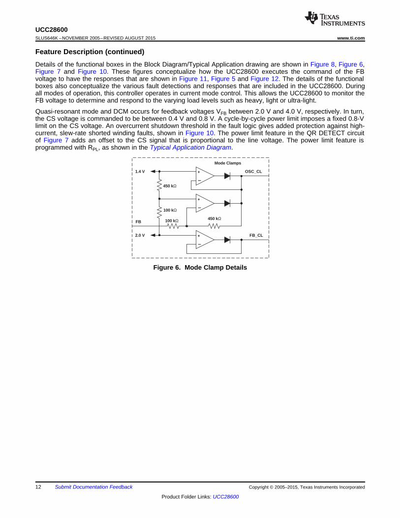
Feature Description (continued)Details of the functional boxes in the Block Diagram/Typical Application drawing are shown in Figure 8, Figure 6,Figure 7 and Figure 10. These figures conceptualize how the UCC28600 executes the command of the FBvoltage to have the responses that are shown in Figure 11, Figure 5 and Figure 12. The details of the functionalboxes also conceptualize the various fault detections and responses that are included in the UCC28600. Duringall modes of operation, this controller operates in current mode control. This allows the UCC28600 to monitor theFB voltage to determine and respond to the varying load levels such as heavy, light or ultra-light.
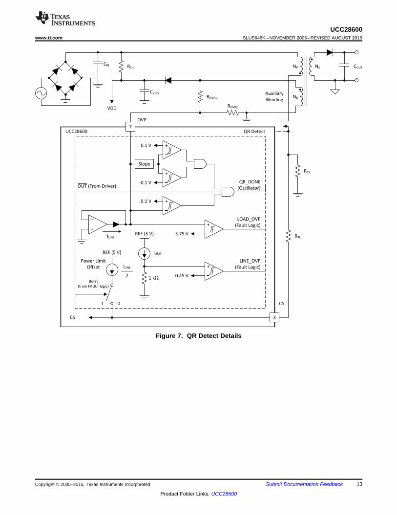
Quasi-resonant mode and DCM occurs for feedback voltages VFB between 2.0 V and 4.0 V, respectively. In turn,the CS voltage is commanded to be between 0.4 V and 0.8 V. A cycle-by-cycle power limit imposes a fixed 0.8-Vlimit on the CS voltage. An overcurrent shutdown threshold in the fault logic gives added protection against high-current, slew-rate shorted winding faults, shown in Figure 10. The power limit feature in the QR DETECT circuitof Figure 7 adds an offset to the CS signal that is proportional to the line voltage. The power limit feature isprogrammed with RPL, as shown in the Typical Application Diagram.
Figure 6. Mode Clamp Details
12 Submit Documentation Feedback Copyright © 2005–2015, Texas Instruments Incorporated
Product Folder Links: UCC28600
RSU
ROVP2
CIN
CVDD
ROVP1
Auxiliary
Winding
+
+
+
+
7
Slope
+
0.1 V
0.1 V
-0.1 V
REF (5 V)
1 k:
3.75 V
0.45 V
QR_DONE
(Oscillator)
LOAD_OVP
(Fault Logic)
LINE_OVP
(Fault Logic)
REF (5 V)
3CS
OVP
VDD
OUT (From Driver)
UCC28600
RPL
CS
RCS
Power Limit
Offset
ILINE
Burst
(from FAULT logic)
01
+
QR Detect
ILINE
ILINE
2
COUTNSNP
NB
UCC28600www.ti.com SLUS646K –NOVEMBER 2005–REVISED AUGUST 2015
Figure 7. QR Detect Details
Copyright © 2005–2015, Texas Instruments Incorporated Submit Documentation Feedback 13
Product Folder Links: UCC28600
OSC_CL
QR_DONE
4.0V
0.1V
SS_MODE
REF
S Q
QRCLK
130 kHz OSC Clamp
Comparator
OSC Valley Comparator
OSC Peak Comparator
RUN
+
+
+
UCC28600SLUS646K –NOVEMBER 2005–REVISED AUGUST 2015 www.ti.com
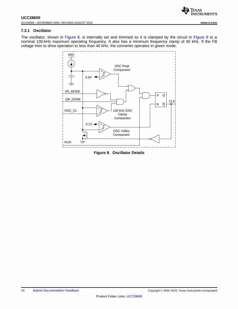
7.3.1 OscillatorThe oscillator, shown in Figure 8, is internally set and trimmed so it is clamped by the circuit in Figure 8 to anominal 130-kHz maximum operating frequency. It also has a minimum frequency clamp of 40 kHz. If the FBvoltage tries to drive operation to less than 40 kHz, the converter operates in green mode.
Figure 8. Oscillator Details
14 Submit Documentation Feedback Copyright © 2005–2015, Texas Instruments Incorporated
Product Folder Links: UCC28600
8
5
VCC
GND
UCC28051
CVCC
0.1 mF
CBULK
2
4
8
6
STATUS
VDD
FB
GND
UCC28600
RST1
RST2
RCS
CVDD
Primary Secondary
10 V
TL431
Feedback
M1
Q1
To Zero
Current
Detection
M2
RVCC
CBIAS
RSU
NB
NP
NS
DZ1
DBIAS
DVDD
UCC28600www.ti.com SLUS646K –NOVEMBER 2005–REVISED AUGUST 2015
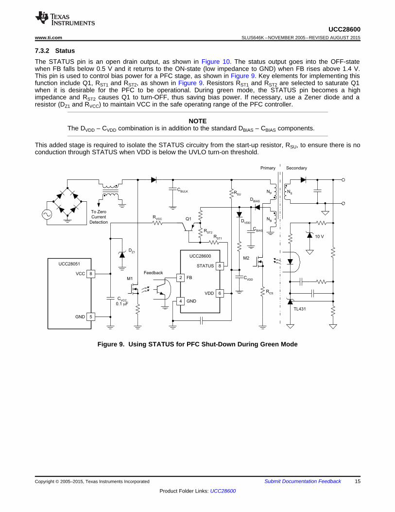
7.3.2 StatusThe STATUS pin is an open drain output, as shown in Figure 10. The status output goes into the OFF-statewhen FB falls below 0.5 V and it returns to the ON-state (low impedance to GND) when FB rises above 1.4 V.This pin is used to control bias power for a PFC stage, as shown in Figure 9. Key elements for implementing thisfunction include Q1, RST1 and RST2, as shown in Figure 9. Resistors RST1 and RST2 are selected to saturate Q1when it is desirable for the PFC to be operational. During green mode, the STATUS pin becomes a highimpedance and RST2 causes Q1 to turn-OFF, thus saving bias power. If necessary, use a Zener diode and aresistor (DZ1 and RVCC) to maintain VCC in the safe operating range of the PFC controller.
NOTEThe DVDD – CVDD combination is in addition to the standard DBIAS – CBIAS components.
This added stage is required to isolate the STATUS circuitry from the start-up resistor, RSU, to ensure there is noconduction through STATUS when VDD is below the UVLO turn-on threshold.
Figure 9. Using STATUS for PFC Shut-Down During Green Mode
Copyright © 2005–2015, Texas Instruments Incorporated Submit Documentation Feedback 15
Product Folder Links: UCC28600

S Q
QR
REF
D Q
Q
CLR
SET
Power-Up Reset
Thermal
Shutdown
+
+1.25 V
0.6 V/0.7 V
+
SS/DIS
RUN
3 CS
OVR_T
LINE_OVP (QR
Detect)
LOAD_OVP
(QR Detect)
VDD_OK
REF_OK
Burst
20 kW
REF
(5 V)
FB
7
FB
CS
SS_MODE
0.6 V/1.5 V
STATUS8
UCC28600
BURST
UCC28600SLUS646K –NOVEMBER 2005–REVISED AUGUST 2015 www.ti.com
7.3.3 Fault LogicAdvanced logic control coordinates the fault detections to provide proper power supply recovery. This providesthe conditioning for the thermal protection. Line overvoltage protection (line OVP) and load OVP areimplemented in this block. It prevents operation when the internal reference is below 4.5 V. If a fault is detectedin the thermal shutdown, line OVP, load OVP, or REF, the UCC28600 undergoes a shutdown/retry cycle.
Refer to the fault logic diagram in Figure 10 and the QR detect diagram in Figure 7 to program line OVP and loadOVP. To program the load OVP, select the ROVP1 – ROVP2 divider ratio to be 3.75 V at the desired output shut-down voltage. To program line OVP, select the impedance of the ROVP1 – ROVP2 combination to draw 450 μAwhen the VOVP is 0.45 V during the ON-time of the power MOSFET at the highest allowable input voltage.
Figure 10. Fault Logic Details
16 Submit Documentation Feedback Copyright © 2005–2015, Texas Instruments Incorporated
Product Folder Links: UCC28600

UCC28600www.ti.com SLUS646K –NOVEMBER 2005–REVISED AUGUST 2015
7.3.4 Protection FeaturesThe UCC28600 has many protection features that are found only on larger, full featured controllers. Refer to theFunctional Block Diagram, Typical Application Diagram, Figure 6, Figure 7, Figure 8, Figure 10, Figure 11, andFigure 12 for detailed block descriptions that show how the features are integrated into the normal controlfunctions.
7.3.5 OvertemperatureOvertemperature lockout typically occurs when the substrate temperature reaches 140°C. Retry is allowed if thesubstrate temperature reduces by the hysteresis value. Upon an overtemperature fault, CSS on softstart isdischarged and STATUS is forced to a high impedance.
7.3.6 Cycle-by-Cycle Power LimitThe cycle terminates when the CS voltage plus the power limit offset exceeds 1.2 V.
In order to have power limited over the full line voltage range of the QR Flyback converter, the CS pin voltagemust have a component that is proportional to the primary current plus a component that is proportional to theline voltage due to predictable switching frequency variations due to line voltage. At power limit, the CS pinvoltage plus the internal CS offset is compared against a constant 1.2-V reference in the PWM comparator. Thusduring cycle-by-cycle power limit, the peak CS voltage is typically 0.8 V.
The current that is sourced from the OVP pin (ILINE) is reflected to a dependent current source of ½ ILINE, that isconnected to the CS pin. The power limit function can be programmed by a resistor, RPL, that is between the CSpin and the current sense resistor. The current, ILINE, is proportional to line voltage by the transformer turns ratioNB/NP and resistor ROVP1. Current ILINE is programmed to set the line over voltage protection. Resistor RPL resultsin the addition of a voltage to the current sense signal that is proportional to the line voltage. The proper amountof additional voltage has the effect of limiting the power on a cycle-by-cycle basis. Note that RCS, RPL, ROVP1 andROVP2 must be adjusted as a set due to the functional interactions.
7.3.7 Primary Current ProtectionWhen the primary current exceeds maximum current level which is indicated by a voltage of 1.25 V at the CSpin, the device initiates a shutdown. Retry occurs after a UVLOOFF or UVLOON cycle. Because the device willinitiate cycle-by-cycle power limit first, primary side current protection is not intended to protect against outputshort circuit conditions. However, this feature does protect the MOSFET against extreme conditions such astransformer saturation.
7.3.8 Over-Voltage ProtectionLine and load over voltage protection is programmed with the transformer turn ratios, ROVP1 and ROVP2. The OVPpin has a 0-V voltage source that can only source current; OVP cannot sink current.
Line over voltage protection occurs when the OVP pin is clamped at 0 V. When the bias winding is negative,during OUT = HI or portions of the resonant ring, the 0-V voltage source clamps OVP to 0 V and the current thatis sourced from the OVP pin is mirrored to the Line_OVP comparator and the QR detection circuit. TheLine_OVP comparator initiates a shutdown-retry sequence if OVP sources any more than 450 μA.
Load-over voltage protection occurs when the OVP pin voltage is positive. When the bias winding is positive,during demagnetization or portions of the resonant ring, the OVP pin voltage is positive. If the OVP voltage isgreater than 3.75 V, the device initiates a shutdown. Retry occurs after a UVLOOFF or UVLOON cycle.
7.3.9 Undervoltage LockoutProtection is provided to guard against operation during unfavorable bias conditions. Undervoltage lockout(UVLO) always monitors VDD to prevent operation below the UVLO threshold.
Copyright © 2005–2015, Texas Instruments Incorporated Submit Documentation Feedback 17
Product Folder Links: UCC28600

VFB
0.5 V 0.7 V 1.4 V 2.0 V 4.0 V 5.0 V
Gre
en M
ode-
ON
, B
urst
-OF
F
Gre
en M
ode-
OF
F,
Bur
st-O
N
Burst Hysteresis
0 V
Green Mode Hysteresis
Green Mode
FFM
40 k
Hz
< f S
< 1
30 k
Hz
VF
B C
ontr
ol R
ange
Lim
it
Inte
rnal
Ref
eren
ce
QR Mode or DCM Mode
UCC28600SLUS646K –NOVEMBER 2005–REVISED AUGUST 2015 www.ti.com
7.4 Device Functional ModesDepending upon the line and load conditions, the UCC28600 controls the converter using different modes ofoperation, which are defined as quasi-resonant (QR mode), discontinuous conduction mode (DCM), frequencyfoldback mode (FFM) and green mode (GM), determined by the voltage on the FB pin, as shown in Figure 11.
For extremely light loads (below approximately 10% full rated power), the converter is controlled using bursts of40-kHz pulses. As the load increases, the number of pulses in these burst packets increases until the converteris switching consistently at 40 kHz, at which point it transitions into the next operating mode, called frequencyfoldback. Frequency foldback mode (FFM) typically begins at loads that are between approximately 10% and upto 30% full rated power, the peak primary side switch current is constant and the output voltage is regulated bymodulating the switching frequency from 40 kHz up to 130 kHz. From approximately 30% to 100% full ratedpower, the UCC28600 controls the converter in either quasi-resonant mode (QRM) or discontinuous conductionmode (DCM). In QRM, the switching frequency will decrease as the load increases; DCM operation is at theclamped maximum switching frequency (130 kHz). The valley detection circuitry is active during FFM, DCM, andQRM operation.
Keep in mind that the aforementioned boundaries of steady-state operation are approximate because they aresubject to converter design parameters.
Figure 11. Mode Control with FB Pin Voltage
18 Submit Documentation Feedback Copyright © 2005–2015, Texas Instruments Incorporated
Product Folder Links: UCC28600
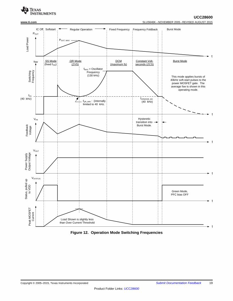
fsw Constant Volt-seconds (ZCS)
Burst Mode
fMAX = Oscillator Frequency(130 kHz)
fQR_MIN : (internally limited to 40 kHz.
QR Mode (ZVS)
Sw
itchi
ng
Fre
quen
cy
VFB
Fee
dbac
k V
olta
ge
VOUT
Pow
er S
uppl
y O
utpu
t Vol
tage
SS Mode (fixed fSW)
t
t
t
fSS (40 kHz) fGRMODE_MX
(40 kHz)
This mode applies bursts of 40kHz soft-start pulses to the power MOSFET gate. The average fsw is shown in this
operating mode.
DCM(maximum fs)
Hysteretic transition into Burst Mode.
Pea
k M
OS
FE
T
Cur
rent
Load Shown is slightly less than Over Current Threshold
t
VSTATUS
Sta
tus,
pul
led
up
to V
DD
t
Green Mode, PFC bias OFF
IC Off Softstart Regular Operation Frequency Foldback Burst ModeFixed Frequency
POUT
Load
Pow
er
t
POUT, MAX
UCC28600www.ti.com SLUS646K –NOVEMBER 2005–REVISED AUGUST 2015
Figure 12. Operation Mode Switching Frequencies
Copyright © 2005–2015, Texas Instruments Incorporated Submit Documentation Feedback 19
Product Folder Links: UCC28600
UCC28600SLUS646K –NOVEMBER 2005–REVISED AUGUST 2015 www.ti.com
7.4.1 Quasi-Resonant and DCM ControlDuring this control mode, the rising edge of OUT will occur just after the valley of the resonant ring when thetransformer is fully demagnetized. Resonant valley switching is an integral part of QR operation. In this mode, theflyback converter operates at the boundary of discontinuous conduction mode and continuous conduction mode.By adjusting both the peak current and the switching frequency, the output power is adjusted to match the loadrequirement. When the load increases, the peak current increases and the switching frequency decreases. Theminimum switching frequency of the converter is limited to 40 kHz. The transformer magnetizing inductor valuehas to be designed accordingly so that the converter can deliver the maximum required power while maintaininga switching frequency that is greater than the fQR(min) over the entire input operating range.
As the load decreases from its designed maximum output power, the UCC28600 will demand a higher switchingfrequency and decreased peak current. The converter’s maximum switching frequency will be limited to 130 kHz.At this maximum switching frequency, the converter enters DCM control. At DCM control, the peak current isadjusted to control the output power. Slight frequency dithering between resonant valleys will occur as the valleydetection is active in DCM control.
Quasi-resonant (QR) and DCM operation occur for feedback voltages, VFB, between 2.0 V and 3.0 V. In turn, thepeak CS voltage is commanded to be between 0.4 V and 0.8 V. The CS pin has an internal dependent currentsource, 1/2 ILINE. This current source adds a proportional step offset (power limit offset) to the CS signal and ispart of the cycle-by-cycle power limit function that is discussed in the Protection Features section.7.4.2 Frequency Foldback Mode ControlOperation in FFM results in the application of constant volt-seconds to the flyback transformer during eachswitching cycle. During frequency foldback mode, as the load decreases, the MOSFET peak current is keptconstant and the switching frequency is reduced (foldback) to reduce the output power. In this mode, the flybackconverter will always operate in discontinuous conduction mode. When the FB voltage is between 1.4 V and2.0 V, the voltage controlled oscillator restricts the operating frequency between 40 kHz and 130 kHz and the CSis clamped to 0.4 V, including the power limit offset. Valley detection is active during FFM.
7.4.3 Green-Mode ControlDuring green mode, the converter operates at a fixed switching frequency of 40 kHz and fixed peak current. Theoutput power is adjusted by the converter ON/OFF durations, which is also known as burst mode. When the FBvoltage is between 1.4 V and 0.5 V, the controller is commanding an excess of energy to be transferred to theload which in turn, drives the error higher and FB lower. When FB reaches 0.5 V, the OUT pulses are terminatedand do not resume until FB reaches 0.7 V. In this mode, the converter operates in hysteretic control with theOUT pulse terminated at a fixed CS voltage level of 0.4 V. The power limit offset is turned OFF during Greenmode and it returns to ON when FB is above 1.4 V. Green mode reduces the average switching frequency inorder to minimize switching losses and increase the efficiency at light-load conditions.
7.4.4 Operating Mode ProgrammingBoundaries of the operating modes are programmed by the flyback transformer and the four components RPL,RCS, ROVP1 and ROVP2; shown in the Functional Block Diagram and Typical Application Diagram drawing.
The transformer characteristics that predominantly affect the modes are the magnetizing inductance of theprimary and the magnitude of the output voltage, reflected to the primary. To a lesser degree (yet significant), theboundaries are affected by the MOSFET output capacitance and transformer leakage inductance. The designprocedure here is to select a magnetizing inductance and a reflected output voltage that operates at theDCM/CCM boundary at maximum load and maximum line. The actual inductance should be noticeably smaller toaccount for the ring between the magnetizing inductance and the total stray capacitance measured at the drainof the power MOSFET. This programs the QR/DCM boundary of operation. All other mode boundaries are presetwith the thresholds in the oscillator and green-mode blocks.
The four components RPL, RCS, ROVP1 and ROVP2 must be programmed as a set due to the interactions of thefunctions. The use of the UCC28600 design calculator, SLVC104, is highly recommended in order to achieve thedesired results with a careful balance between the transformer parameters and the programming resistors.
20 Submit Documentation Feedback Copyright © 2005–2015, Texas Instruments Incorporated
Product Folder Links: UCC28600

UCC28600www.ti.com SLUS646K –NOVEMBER 2005–REVISED AUGUST 2015
8 Application and Implementation
NOTEInformation in the following Applications section is not part of the TI componentspecification, and TI does not warrant its accuracy or completeness. TI’s customersare responsible for determining suitability of components for their purposes.Customers should validate and test their design implementation to confirm systemfunctionality.
8.1 Application InformationThe UCC28600 device is a flyback controller that operates in a mode that is determined by the FB voltage. Lineand load conditions set the FB voltage and the controller will operate in Green Mode (GM) under light-loadconditions, Frequency Foldback Mode (FFM) when operating at loads approximately between 10% and 30% fullrated load, and Quasi-Resonant (QR) or Discontinuous Mode (DCM) at higher loads. Valley switching under allmodes, except green mode, reduces switching losses and improves efficiency. Valley skipping also helps reduceEMI. A dedicated STATUS pin is used in higher power applications that use a power factor corrected (PFC) frontend. Under light-load conditions, the STATUS signal can be used to disconnect the bias power to the PFCcontroller, reducing light-load power consumption.
8.2 Typical ApplicationA typical application for the UCC28600 is an off-line flyback controller from 65 W to 120 W, using a PFC outputvoltage as its input, as shown in Figure 13. The PFC stage is assumed to operate from a universal AC input andcan be controlled by a device such as the UCC28051. The auxiliary winding provides the bias to the controllersand provides over voltage protection and valley switching information, as well as bias to the UCC28600 andUCC28051. The UCC28600 will disable the PFC controller during green mode operation, improving light-loadsystem efficiency. The series resistor connected between the current sense pin and the current sense resistorprograms the power limit of the converter. Low valley voltage switching and multi-mode operation will keep theefficiency curve high over the entire operation range. Typical applications include bias supplies for LCD monitors,LCD and PDP televisions, set top boxes, AC-DC adaptors, and energy efficient power supplies up to 200 W.
Copyright © 2005–2015, Texas Instruments Incorporated Submit Documentation Feedback 21
Product Folder Links: UCC28600

CBULK
FEEDBACK
CSS
RCS
ROVP1
ROVP2
CVDD
D1
RSU
RPL
TL431
2
1
6
SS
VDD
4 GND 5OUT
FB
8
3 CS
7OVP
STATUS
UCC28600
CBP
100nF
RST2
RST1
COUT
PRIMARY SECONDARY
N1
NB
N2 VOUT
+
-
+
-
VBULK
ICC
RVDD
QST
ROUTRSNUB CSNUB
M1
PFC OUTPUT
or
BRIDGE RECTIFIER
PFC CONTROLLER BIAS
(if used)
CBIAS
D2
UCC28600SLUS646K –NOVEMBER 2005–REVISED AUGUST 2015 www.ti.com
Typical Application (continued)
Figure 13. Simplified Application
22 Submit Documentation Feedback Copyright © 2005–2015, Texas Instruments Incorporated
Product Folder Links: UCC28600
UCC28600www.ti.com SLUS646K –NOVEMBER 2005–REVISED AUGUST 2015
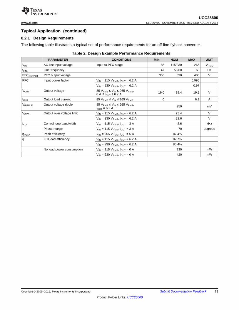
Typical Application (continued)8.2.1 Design RequirementsThe following table illustrates a typical set of performance requirements for an off-line flyback converter.
Table 2. Design Example Performance RequirementsPARAMETER CONDITIONS MIN NOM MAX UNIT
VIN AC line input voltage Input to PFC stage 85 115/230 265 VRMS
fLINE Line frequency 47 50/60 63 HzPFCOUTPUT PFC output voltage 350 390 400 VPFC Input power factor VIN = 115 VRMS, IOUT = 6.2 A 0.998
VIN = 230 VRMS, IOUT = 6.2 A 0.97VOUT Output voltage 85 VRMS ≤ VIN ≤ 265 VRMS, 19.0 19.4 19.8 V0 A ≤ IOUT ≤ 6.2 AIOUT Output load current 85 VRMS ≤ VIN ≤ 265 VRMS 0 6.2 AVRIPPLE Output voltage ripple 85 VRMS ≤ VIN ≤ 265 VRMS, 250 mVIOUT = 6.2 AVOVP Output over voltage limit VIN = 115 VRMS, IOUT = 6.2 A 23.4 V
VIN = 230 VRMS, IOUT = 6.2 A 23.6 VfCO Control loop bandwidth VIN = 115 VRMS, IOUT = 3 A 2.6 kHz
Phase margin VIN = 115 VRMS, IOUT = 3 A 70 degreesηPEAK Peak efficiency VIN = 265 VRMS, IOUT = 6 A 87.4%η Full load efficiency VIN = 115 VRMS, IOUT = 6.2 A 82.7%
VIN = 230 VRMS, IOUT = 6.2 A 86.4%No load power consumption VIN = 115 VRMS, IOUT = 0 A 230 mW
VIN = 230 VRMS, IOUT = 0 A 420 mW
Copyright © 2005–2015, Texas Instruments Incorporated Submit Documentation Feedback 23
Product Folder Links: UCC28600
2 2
12 0.25 arcsin
2
ª º§ ·« »¨ ¸u u« »¨ ¸
© ¹¬ ¼t u
BULK minIN
PFCoutput min
BULK
PFCoutput min BULK min LINE min
VP
9
CV V f
u
OUT OUT maxOUT
IN max
V IPP
UCC28600SLUS646K –NOVEMBER 2005–REVISED AUGUST 2015 www.ti.com
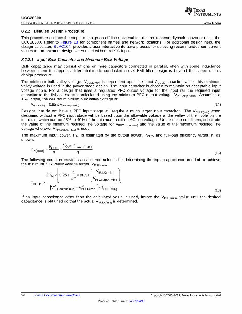
8.2.2 Detailed Design ProcedureThis procedure outlines the steps to design an off-line universal input quasi-resonant flyback converter using theUCC28600. Refer to Figure 13 for component names and network locations. For additional design help, thedesign calculator, SLVC104, provides a user-interactive iterative process for selecting recommended componentvalues for an optimum design when used without a PFC input.
8.2.2.1 Input Bulk Capacitor and Minimum Bulk VoltageBulk capacitance may consist of one or more capacitors connected in parallel, often with some inductancebetween them to suppress differential-mode conducted noise. EMI filter design is beyond the scope of thisdesign procedure.
The minimum bulk valley voltage, VBULK(min) is dependent upon the input CBULK capacitor value; this minimumvalley voltage is used in the power stage design. The input capacitor is chosen to maintain an acceptable inputvoltage ripple. For a design that uses a regulated PFC output voltage for the input rail the required inputcapacitor to the flyback stage is calculated using the minimum PFC output voltage, VPFCoutput(min). Assuming a15% ripple, the desired minimum bulk valley voltage is:
VBULK(min) = 0.85 x VPFCoutput(min) (14)
Designs that do not have a PFC input stage will require a much larger input capacitor. The VBULK(min) whendesigning without a PFC input stage will be based upon the allowable voltage at the valley of the ripple on theinput rail, which can be 25% to 40% of the minimum rectified AC line voltage. Under those conditions, substitutethe value of the minimum rectified line voltage for VPFCoutput(min) and the value of the maximum rectified linevoltage wherever VPFCoutput(max) is used.
The maximum input power, PIN, is estimated by the output power, POUT, and full-load efficiency target, η, asshown:
(15)
The following equation provides an accurate solution for determining the input capacitance needed to achievethe minimum bulk valley voltage target, VBULK(min):
(16)
If an input capacitance other than the calculated value is used, iterate the VBULK(min) value until the desiredcapacitance is obtained so that the actual VBULK(min) is determined.
24 Submit Documentation Feedback Copyright © 2005–2015, Texas Instruments Incorporated
Product Folder Links: UCC28600

1
0.925u u u u
u u
OUT F PS SWBULK minP
P BULKmin PS OUT F
V V V N tI
L V N V V
12
u
u
OVP OVP loadOVP
PSFOUT shutdown OVP load
PB
R VR
NV V V
N
1
u
BULK OVPOVP
PB OVP line
VR
N I
20.925
2
ª ºu u u u« » u« » u u ¬ ¼
OUT F PS SWBULK min SWP max
IN maxPS OUT FBULK min
V V V N t fL
PV N V V
uOUT
PB PSBIAS
VN N
V
FLYBACKPS
OUT F
VN
V V
1.5
DS max PFCoutput maxFLYBACK
V VV
UCC28600www.ti.com SLUS646K –NOVEMBER 2005–REVISED AUGUST 2015
8.2.2.2 Transformer Turns Ratio and Primary InductanceThe allowable flyback voltage, VFLYBACK, seen by the MOSFET, determines the minimum primary to secondaryturns-ratio, NPS. The flyback voltage is calculated based upon the acceptable Drain to Source voltage rating ofthe MOSFET and the maximum PFC output voltage rail, VPFCoutput(max) (or rectified maximum line voltage if notusing a PFC input stage), and derating to account for voltage spikes due to leakage inductance:
(17)
Typically, in an off-line design or a design with a PFC output voltage of 390 VDC to 400 VDC, a MOSFET ratedfor VDS(max) of 600 VDS or greater is used. The primary to secondary turns-ratio takes the output diode voltagedrop, VF, into account:
(18)
The primary to bias winding turns ratio is calculated, based upon the desired bias voltage, VBIAS, for theUCC28600 controller and the PFC controller bias voltage, making sure to avoid the absolute maximum rating forVDD of each controller:
(19)
The switching frequency at the minimum bulk valley voltage is used as a limiting factor for the maximum primaryinductance. The UCC28600 will operate in quasi-resonant mode during operation at maximum load, minimuminput voltage and its peak primary current and its switching frequency will be modulated during each switchingcycle. Using a switching frequency of 80 kHz, for fSW, at this operating point will give adequate margin formanufacturing tolerances in the transformer, the parasitic switch node capacitance, which influences theresonant frequency to each valley, and keep the controller from trying to go continuous during transientconditions. The switching period, tSW, is equal to 1/fSW. Using volt-second balance, the maximum primaryinductance can be calculated:
(20)
The resistor divider on OVP senses the line voltage during the switch on-time when the auxiliary winding voltageis proportional to the line voltage. During this portion of the switching cycle, the OVP pin is internally clamped toapproximately 0 V and sources current proportional to the line voltage. The ROVP1 resistor is chosen using thenominal line over-voltage protection current threshold, IOVP(line), which is equal to 450 µA.
(21)
The OVP pin is also used to sense the output voltage when the OUT signal is low. To set the output over-voltage level, VOUT(shutdown), which is the desired voltage level on the output that would cause the controller toshutdown, use the load overvoltage protection threshold, VOVP(load), equal to 3.75 V, to determine the requiredROVP2 resistor.
(22)
The peak primary current at low input voltage, full load, IP(1), can be estimated with the following equation:
(23)
Copyright © 2005–2015, Texas Instruments Incorporated Submit Documentation Feedback 25
Product Folder Links: UCC28600

2 1
1 2 2 1
u
u u
PL CS os P PPL
CS P CS P
V V I IR
I I I I
2 1
2 1 1 2
u
u u
PL CS os CS CSCS
CS P CS P
V V I IR
I I I I
21 2 1
1 10.5 550
ª º§ ·« » u u ¨ ¸
u« »© ¹¬ ¼
PFCoutput maxCS
OVP OVP PB OVP
VI mV
R R N R
11 2 1
1 10.5 550
ª º§ ·« » u u ¨ ¸
u« »© ¹¬ ¼
BULK minCS
OVP OVP PB OVP
VI mV
R R N R
2
0.925ª º« »u u u« »¬ ¼
ª ºu u « »¬ ¼
PS OUT FPFCoutput maxSWvin max
PP PS OUT F PFCoutput max
V N V Vf
IL N V V V
22 2 2
2
0.925
2
u u u
ª ºu u u u « »¬ ¼
PS OUT FPFCoutput maxSWvin max
P INmax PS OUT FPFCoutput max
N V V Vf
L P V N V V
UCC28600SLUS646K –NOVEMBER 2005–REVISED AUGUST 2015 www.ti.com
The switching frequency at maximum input voltage can be estimated:
(24)
Now that the switching frequency at the maximum input voltage has been determined, the peak primary currentat maximum load, IP(2), at the maximum input voltage can be calculated:
(25)
The power limit current that is sourced at the CS pin adds a voltage step to the CS waveform that is proportionalto the line voltage. At minimum input voltage, maximum load, this current is referred to as ICS(1) and can beestimated from the following equation:
(26)
At maximum input voltage and maximum load, the power limit current sourced from CS is referred to as ICS(2) andis estimated using the same formula:
(27)
The appropriate values of the current sense resistor, RCS, and the power limit resistor, RPL, are both dependentupon the internal power limit threshold, VPL = 1.20 V, the CS offset voltage, VCS(os) = 0.40 V, peak primarycurrents, and the power limit currents, calculated above, and can be calculated as shown:
(28)
(29)
26 Submit Documentation Feedback Copyright © 2005–2015, Texas Instruments Incorporated
Product Folder Links: UCC28600
RCS
RPL1
RPL2
From power MOSFET
To CS
RDCS
RPL
From power MOSFET
To CS
(a) (b)
CS
DCS
RR
1
§ ·
¨ ¸© ¹
PL1PL2
RR
PL1 PL
CS
DCSR R
R
R u
UCC28600www.ti.com SLUS646K –NOVEMBER 2005–REVISED AUGUST 2015
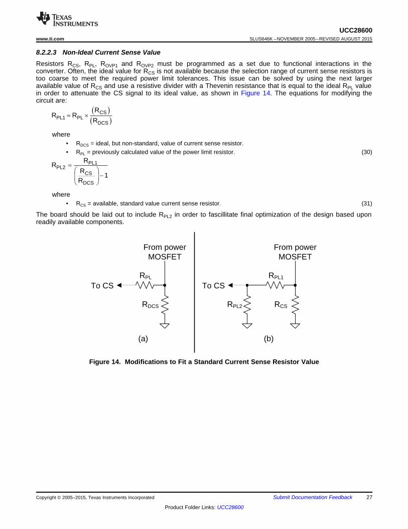
8.2.2.3 Non-Ideal Current Sense ValueResistors RCS, RPL, ROVP1 and ROVP2 must be programmed as a set due to functional interactions in theconverter. Often, the ideal value for RCS is not available because the selection range of current sense resistors istoo coarse to meet the required power limit tolerances. This issue can be solved by using the next largeravailable value of RCS and use a resistive divider with a Thevenin resistance that is equal to the ideal RPL valuein order to attenuate the CS signal to its ideal value, as shown in Figure 14. The equations for modifying thecircuit are:
where• RDCS = ideal, but non-standard, value of current sense resistor.• RPL = previously calculated value of the power limit resistor. (30)
where• RCS = available, standard value current sense resistor. (31)
The board should be laid out to include RPL2 in order to fascillitate final optimization of the design based uponreadily available components.
Figure 14. Modifications to Fit a Standard Current Sense Resistor Value
Copyright © 2005–2015, Texas Instruments Incorporated Submit Documentation Feedback 27
Product Folder Links: UCC28600
CBULK
RCS
DS
RSNUB1LM
PRIMARY SECONDARY
CSNUB
CDM1
VIN
+
-
VG
+
-
VD
+
-
CBULK
RCS
DS
RSNUB1
LM
PRIMARY SECONDARY
CSNUB
RSNUB2
CDM1
VIN
+
-
VG
+
-
VD
+
-
(a)
(c)
'VSNUB
VBULK
0V
VR
VD
VG
0V
LLEAK CD Resonance
(b)
'VSNUB
VBULK
0V
VD
VG
0V
Reduced LLEAK CD Resonance
VR
(d)
LLEAK
LLEAK
UCC28600SLUS646K –NOVEMBER 2005–REVISED AUGUST 2015 www.ti.com
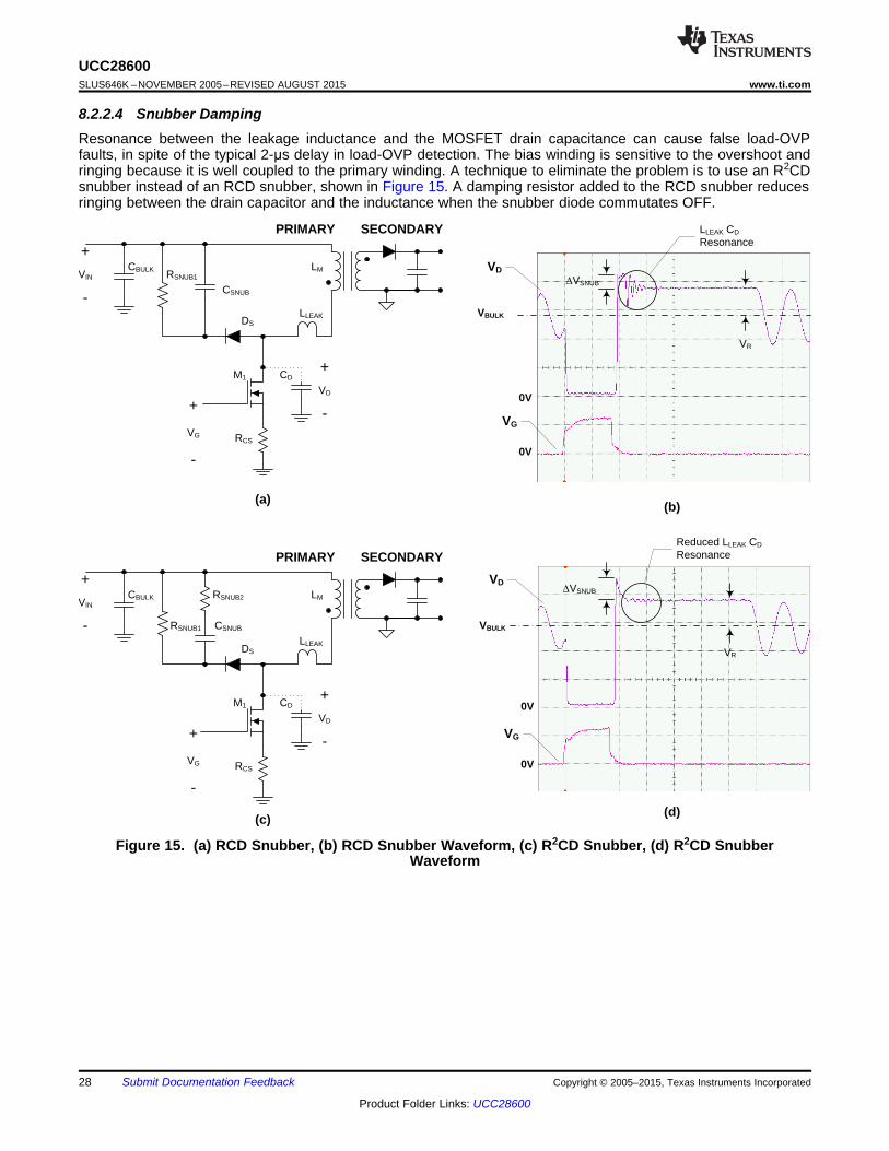
8.2.2.4 Snubber DampingResonance between the leakage inductance and the MOSFET drain capacitance can cause false load-OVPfaults, in spite of the typical 2-μs delay in load-OVP detection. The bias winding is sensitive to the overshoot andringing because it is well coupled to the primary winding. A technique to eliminate the problem is to use an R2CDsnubber instead of an RCD snubber, shown in Figure 15. A damping resistor added to the RCD snubber reducesringing between the drain capacitor and the inductance when the snubber diode commutates OFF.
Figure 15. (a) RCD Snubber, (b) RCD Snubber Waveform, (c) R2CD Snubber, (d) R2CD SnubberWaveform
28 Submit Documentation Feedback Copyright © 2005–2015, Texas Instruments Incorporated
Product Folder Links: UCC28600
R
SNUB
2VQ 1
V
'
LEAK S(max)2SNUB CS(peak) SNUB2
SNUBR
L f1P R I R
V3V
2
ª º« »« »
'« »§ ·¨ ¸« »
© ¹¬ ¼
SNUBSNUB2
CS(peak)
VR
I
§ ·' ¨ ¸¨ ¸© ¹
( )
2
2
SNUB
R
R
SNUB
SNUB1
SNUB1
V 1 1V 1
V 12 3
V 2P R
R
é ùé ùê úê úDæ ö æ öê úê ú+ ´ + ´ç ÷ç ÷ ê úè ø ê úè ø +ê úê úë ûë û=
LEAK CS(peak)RSNUB
SNUB SNUB SNUB
L IV1 1R
2 V C V
§ ·§ · ¨ ¸¨ ¸
' '© ¹ © ¹
2CS(peak) LEAK
SNUB 2R SNUB R
I LC
V V 2 V
'
SNUB
R
VPick between0.5and1
V'
UCC28600www.ti.com SLUS646K –NOVEMBER 2005–REVISED AUGUST 2015
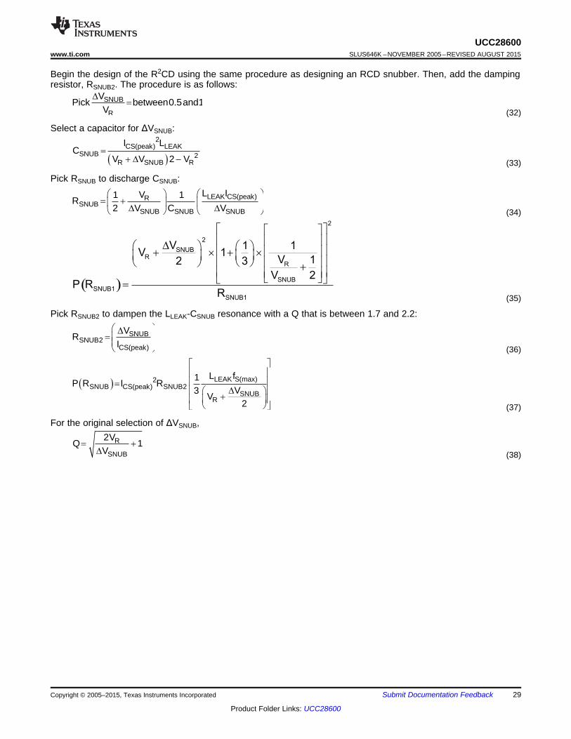
Begin the design of the R2CD using the same procedure as designing an RCD snubber. Then, add the dampingresistor, RSNUB2. The procedure is as follows:
(32)
Select a capacitor for ΔVSNUB:
(33)
Pick RSNUB to discharge CSNUB:
(34)
(35)
Pick RSNUB2 to dampen the LLEAK-CSNUB resonance with a Q that is between 1.7 and 2.2:
(36)
(37)
For the original selection of ΔVSNUB,
(38)
Copyright © 2005–2015, Texas Instruments Incorporated Submit Documentation Feedback 29
Product Folder Links: UCC28600
CSS
3.3 nF ROVP
500
RCST 37.4k,
See note
SS
VDD
GND OUT
FB
CS
OVP
STATUS
UCC28600
CDD
100 nF
COUT
1.0nF
ROUT
10
CBIAS
1 PF
CCST 560 pF,
See note
CFBT
47 pF
+ 5V
VDDIDD
V(FB)
V(CS)
V(OVP)IOVP
V(OUT)
STATUS
GND
ICS
1
2
3
4 5
6
7
8
UCC28600SLUS646K –NOVEMBER 2005–REVISED AUGUST 2015 www.ti.com
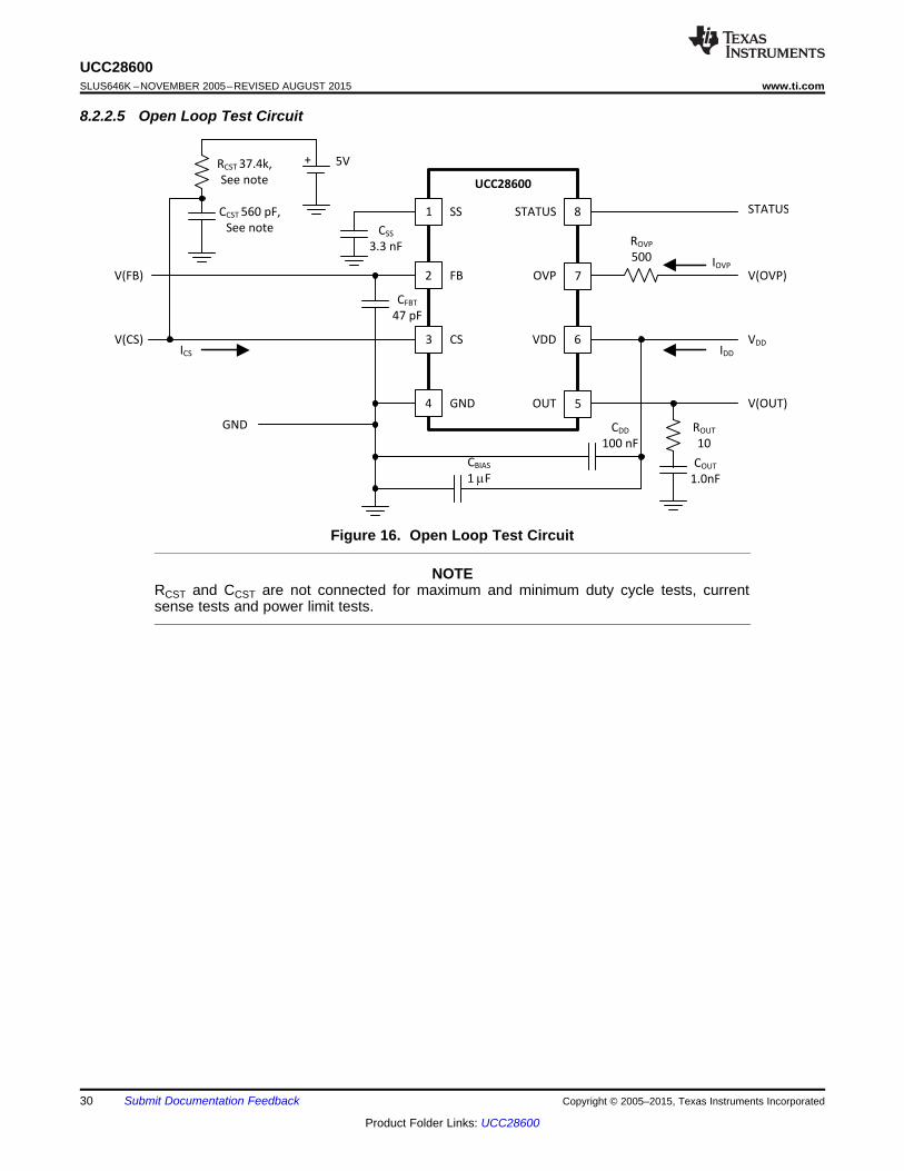
8.2.2.5 Open Loop Test Circuit
Figure 16. Open Loop Test Circuit
NOTERCST and CCST are not connected for maximum and minimum duty cycle tests, currentsense tests and power limit tests.
30 Submit Documentation Feedback Copyright © 2005–2015, Texas Instruments Incorporated
Product Folder Links: UCC28600
0.0
VO
UT -
Ou
tpu
t V
olt
age
- V
10
15
25
20
0.0 12
IOUT - Output Current - A
2 104 6 8
5
t - Time - 2.50 Ps/div.
DrainCH1: 200 V/div.
GateCH2: 10 V/div.
FBCH3: 5.0 V/div.
CSCH4: 1.0 V/div.
t - Time - 2.50 Ps/div.
DrainCH1: 200 V/div.
GateCH2:10 V/div.
FBCH3:5.0 V/div.
CSCH4:1.0 V/div.
t - Time - 2.50 Ps/div.
DrainCH1: 200 V/div.
GateCH2:10 V/div.
FBCH3:5.0 V/div.
CSCH4:1.0 V/div.
t - Time - 200 Ps/div.
DrainCH1: 200 V/div.
GateCH1: 10 V/div.
FBCH1: 1.0 V/div.
CSCH1: 500 mV/div.
t - Time - 25 Ps/div.
DrainCH1: 200 V/div.
GateCH2: 10 V/div.
FBCH3: 1.0 V/div.
CSCH4: 500 mV/div.
UCC28600www.ti.com SLUS646K –NOVEMBER 2005–REVISED AUGUST 2015
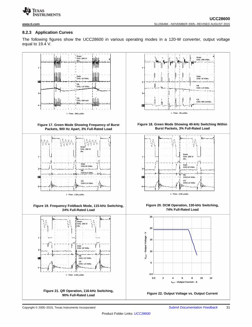
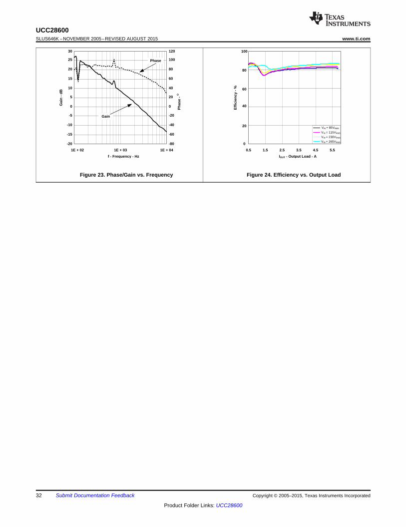
8.2.3 Application CurvesThe following figures show the UCC28600 in various operating modes in a 120-W converter, output voltageequal to 19.4 V.
Figure 18. Green Mode Showing 40-kHz Switching WithinFigure 17. Green Mode Showing Frequency of BurstBurst Packets, 3% Full-Rated LoadPackets, 900 Hz Apart, 3% Full-Rated Load
Figure 20. DCM Operation, 130-kHz Switching,Figure 19. Frequency Foldback Mode, 115-kHz Switching,74% Full-Rated Load24% Full-Rated Load
Figure 21. QR Operation, 116-kHz Switching,Figure 22. Output Voltage vs. Output Current90% Full-Rated Load
Copyright © 2005–2015, Texas Instruments Incorporated Submit Documentation Feedback 31
Product Folder Links: UCC28600
-20
Gai
n -
dB
0
10
30
-15
-5
5
20
25
1E + 02 1E + 04
f - Frequency - Hz
1E + 03
-10
15
Gain
Phase
-80
0
40
120
-60
-20
20
80
100
-40
60
Ph
ase
- O
0
Eff
icie
ncy
- %
100
20
0.5
IOUT - Output Load - A
2.5 3.51.5 4.5 5.5
40
60
80
VIN = 85VRMS
VIN = 115VRMS
VIN = 230VRMS
VIN = 265VRMS
UCC28600SLUS646K –NOVEMBER 2005–REVISED AUGUST 2015 www.ti.com
Figure 23. Phase/Gain vs. Frequency Figure 24. Efficiency vs. Output Load
32 Submit Documentation Feedback Copyright © 2005–2015, Texas Instruments Incorporated
Product Folder Links: UCC28600
UCC28600www.ti.com SLUS646K –NOVEMBER 2005–REVISED AUGUST 2015
8.3 Do's and Don'tsAlways be sure to do the following:• Isolate the STATUS pin from the start up resistor with a diode to prevent the bias current from the bulk input
rail from being diverter away from VDD and into STATUS circuit.• Use a bypass capacitor on VDD, minimum value of 0.1 µF, to filter high frequency noise.• Use a large bulk capacitor on VDD to hold the bias above the UVLO turn off threshold between the long
periods of time between burst packets at light load.• Use a large enough capacitor on SS to prevent triggering power limit when charging the output capacitor
bank at turn on.• Place the SS capacitor as close as possible to the SS pin with short traces and return to the quiet signal
ground.• Design the loop crossover frequency to be between 2 kHz to 3 kHz at nominal input voltage and 50% load
with a phase margin of 70 degrees to satisfactorily stabilize the loop for the entire range of operation.• Add a small filter capacitor to CS to effectively create an RC low pass filter in conjunction with the power limit
resistor, RPL, which will improve noise immunity at the current sense pin.• Place a 10-kΩ resistor between the gate of the MOSFET and ground to discharge the gate capacitance and
protect against inadvertent dv/dt triggered turn-on.• Use a small value gate drive resistor in series with the gate drive to control the turn on transition time and
reduce the dv/dt ringing in this node.• Select the ROVP1, ROVP2, RPL, and RCS together as the OVP resistors set up an internal dependent current
source that impact the RCS and RPL component values.• Design the transformer so the bias winding is well coupled to both the primary winding and the secondary
winding. The bias winding is used not only for VDD bias but also for valley detection, line over-voltage, loadover-voltage, and power limit off-set current.
CAUTIONDo not use a filter capacitor larger than 390 pF on the FB pin, this capacitor willprovide a delay time to over-load response; capacitors larger than 390 pF willadversely affect performance.
Copyright © 2005–2015, Texas Instruments Incorporated Submit Documentation Feedback 33
Product Folder Links: UCC28600
UCC28600SLUS646K –NOVEMBER 2005–REVISED AUGUST 2015 www.ti.com
9 Power Supply RecommendationsThe UCC28600 is intended for AC-to-DC adaptors with input voltage range of 85 VAC(rms) to 265 VAC(rms) usingthe flyback topology. This controller can be used in supplies from a few Watts of power up to 200 Watts limitedonly by the practical use of a DCM flyback in regards to peak currents and output capacitor component size.The UCC28600 can be used in bias supplies for LCD monitors, TVs, and set-top boxes, as well as AC-to-DCadapters for energy-efficient supplies.
10 Layout
10.1 Layout GuidelinesTo increase the reliability and feasibility of the design it is recommended to adhere to the following guidelines forPCB layout.1. Minimize the high current loops to reduce parasitic capacitances and inductances. At the same time, do not
inadvertently make traces with a high dv/dt too wide as this will create a very good E-field antenna.2. Separate the device signal ground from the high current power ground in order to isolate the noise away
from the device substrate. The separate grounds should, ideally, be tied together at the input capacitor onthe primary side.
3. Return the sense resistor to the ground side of the input capacitor, instead of to the ground plane under thedevice.
4. The bypass capacitor on VDD must be placed as close as possible to the VDD and GND pins of the device.5. The filter capacitor on CS must be placed as close as possible to the CS pin and GND pin of the device.6. The filter capacitor on FB must be placed as close as possible to the FB and GND pins of the device.
34 Submit Documentation Feedback Copyright © 2005–2015, Texas Instruments Incorporated
Product Folder Links: UCC28600
VDD
OUT
CS
GND
UCC28600
STATUSSS
FB OVP ROVP1
ROVP2
CCS
RCS
RPL
CSS
CFB
CV
DD
3
GDS
RGS
RG
RVDD
RSU
To AUX Winding
To PGND
To VBULK
To PRIWinding
To PGND
CBULK
To VBULK
To PGND
UCC28600www.ti.com SLUS646K –NOVEMBER 2005–REVISED AUGUST 2015
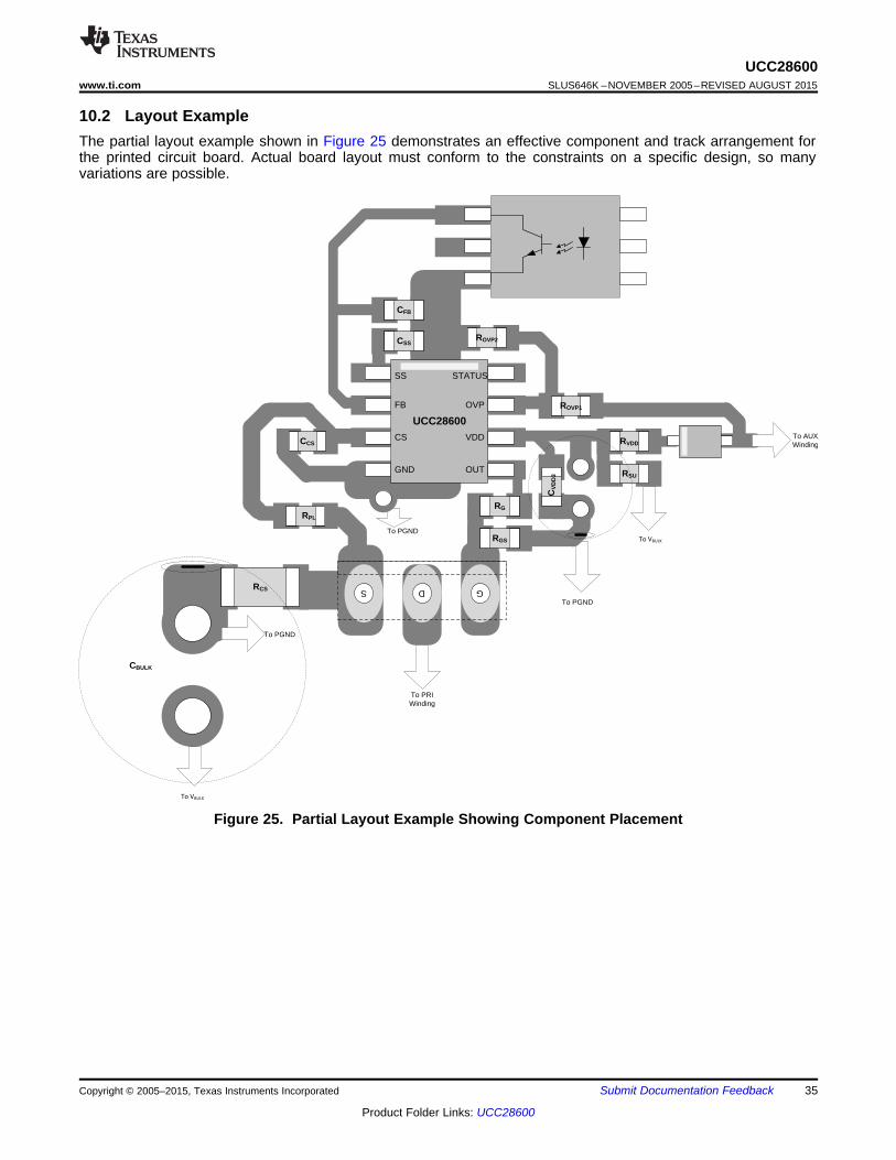
10.2 Layout ExampleThe partial layout example shown in Figure 25 demonstrates an effective component and track arrangement forthe printed circuit board. Actual board layout must conform to the constraints on a specific design, so manyvariations are possible.
Figure 25. Partial Layout Example Showing Component Placement
Copyright © 2005–2015, Texas Instruments Incorporated Submit Documentation Feedback 35
Product Folder Links: UCC28600
UCC28600SLUS646K –NOVEMBER 2005–REVISED AUGUST 2015 www.ti.com
11 Device and Documentation Support
11.1 Device Support
11.1.1 Development SupportUCC28600 Design Calculator, A QR Flyback Designer.xls, spreadsheet for Microsoft Excel 2003, (SLVC104)
11.2 Documentation Support
11.2.1 Related Documentation• Power Supply Seminar SEM-1400 Topic 2: Design And Application Guide For High Speed MOSFET Gate
Drive Circuits, by Laszlo Balogh, (SLUP169)• Datasheet, UCC3581 Micro Power PWM Controller, (SLUS295)• Datasheet, UCC28051 Transition Mode PFC Controller, (SLUS515)• Design Considerations for the UCC28600, (SLUA399)
11.2.2 Related Products• UCC28051 Transition Mode PFC Controller (SLUS515)• UCC3581 Micro Power PWM Controller (SLUS295)
11.3 TrademarksTrueDrive is a trademark of Texas Instruments.All other trademarks are the property of their respective owners.
11.4 Electrostatic Discharge CautionThese devices have limited built-in ESD protection. The leads should be shorted together or the device placed in conductive foamduring storage or handling to prevent electrostatic damage to the MOS gates.
11.5 GlossarySLYZ022 — TI Glossary.
This glossary lists and explains terms, acronyms, and definitions.
36 Submit Documentation Feedback Copyright © 2005–2015, Texas Instruments Incorporated
Product Folder Links: UCC28600
UCC28600www.ti.com SLUS646K –NOVEMBER 2005–REVISED AUGUST 2015
12 Mechanical, Packaging, and Orderable InformationThe following pages include mechanical, packaging, and orderable information. This information is the mostcurrent data available for the designated devices. This data is subject to change without notice and revision ofthis document. For browser-based versions of this data sheet, refer to the left-hand navigation.
Copyright © 2005–2015, Texas Instruments Incorporated Submit Documentation Feedback 37
Product Folder Links: UCC28600
PACKAGE OPTION ADDENDUM
www.ti.com 13-Aug-2021
Addendum-Page 1
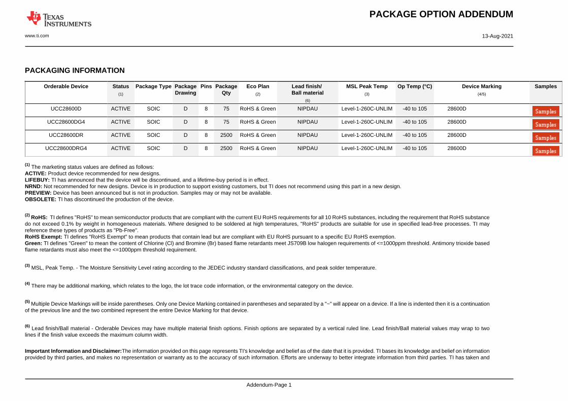
PACKAGING INFORMATION
Orderable Device Status(1)
Package Type PackageDrawing
Pins PackageQty
Eco Plan(2)
Lead finish/Ball material
(6)
MSL Peak Temp(3)
Op Temp (°C) Device Marking(4/5)
Samples
UCC28600D ACTIVE SOIC D 8 75 RoHS & Green NIPDAU Level-1-260C-UNLIM -40 to 105 28600D
UCC28600DG4 ACTIVE SOIC D 8 75 RoHS & Green NIPDAU Level-1-260C-UNLIM -40 to 105 28600D
UCC28600DR ACTIVE SOIC D 8 2500 RoHS & Green NIPDAU Level-1-260C-UNLIM -40 to 105 28600D
UCC28600DRG4 ACTIVE SOIC D 8 2500 RoHS & Green NIPDAU Level-1-260C-UNLIM -40 to 105 28600D
(1) The marketing status values are defined as follows:ACTIVE: Product device recommended for new designs.LIFEBUY: TI has announced that the device will be discontinued, and a lifetime-buy period is in effect.NRND: Not recommended for new designs. Device is in production to support existing customers, but TI does not recommend using this part in a new design.PREVIEW: Device has been announced but is not in production. Samples may or may not be available.OBSOLETE: TI has discontinued the production of the device.
(2) RoHS: TI defines "RoHS" to mean semiconductor products that are compliant with the current EU RoHS requirements for all 10 RoHS substances, including the requirement that RoHS substancedo not exceed 0.1% by weight in homogeneous materials. Where designed to be soldered at high temperatures, "RoHS" products are suitable for use in specified lead-free processes. TI mayreference these types of products as "Pb-Free".RoHS Exempt: TI defines "RoHS Exempt" to mean products that contain lead but are compliant with EU RoHS pursuant to a specific EU RoHS exemption.Green: TI defines "Green" to mean the content of Chlorine (Cl) and Bromine (Br) based flame retardants meet JS709B low halogen requirements of <=1000ppm threshold. Antimony trioxide basedflame retardants must also meet the <=1000ppm threshold requirement.
(3) MSL, Peak Temp. - The Moisture Sensitivity Level rating according to the JEDEC industry standard classifications, and peak solder temperature.
(4) There may be additional marking, which relates to the logo, the lot trace code information, or the environmental category on the device.
(5) Multiple Device Markings will be inside parentheses. Only one Device Marking contained in parentheses and separated by a "~" will appear on a device. If a line is indented then it is a continuationof the previous line and the two combined represent the entire Device Marking for that device.
(6) Lead finish/Ball material - Orderable Devices may have multiple material finish options. Finish options are separated by a vertical ruled line. Lead finish/Ball material values may wrap to twolines if the finish value exceeds the maximum column width.
Important Information and Disclaimer:The information provided on this page represents TI's knowledge and belief as of the date that it is provided. TI bases its knowledge and belief on informationprovided by third parties, and makes no representation or warranty as to the accuracy of such information. Efforts are underway to better integrate information from third parties. TI has taken and
PACKAGE OPTION ADDENDUM
www.ti.com 13-Aug-2021
Addendum-Page 2
continues to take reasonable steps to provide representative and accurate information but may not have conducted destructive testing or chemical analysis on incoming materials and chemicals.TI and TI suppliers consider certain information to be proprietary, and thus CAS numbers and other limited information may not be available for release.
In no event shall TI's liability arising out of such information exceed the total purchase price of the TI part(s) at issue in this document sold by TI to Customer on an annual basis.
OTHER QUALIFIED VERSIONS OF UCC28600 :
• Automotive : UCC28600-Q1
NOTE: Qualified Version Definitions:
• Automotive - Q100 devices qualified for high-reliability automotive applications targeting zero defects
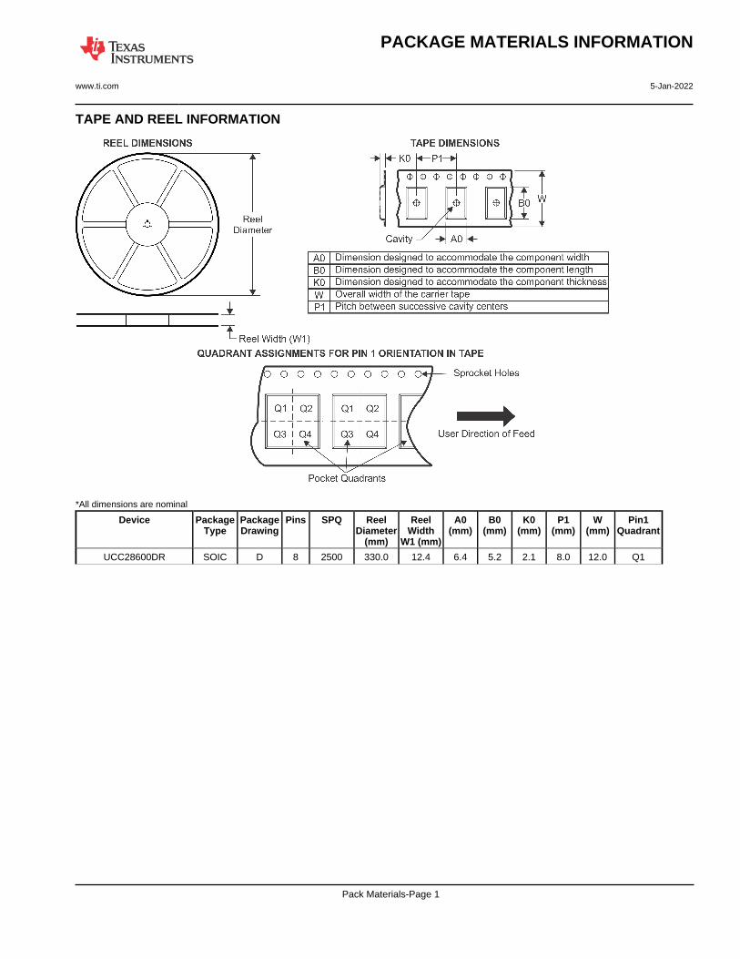
TAPE AND REEL INFORMATION
*All dimensions are nominal
Device PackageType
PackageDrawing
Pins SPQ ReelDiameter
(mm)
ReelWidth
W1 (mm)
A0(mm)
B0(mm)
K0(mm)
P1(mm)
W(mm)
Pin1Quadrant
UCC28600DR SOIC D 8 2500 330.0 12.4 6.4 5.2 2.1 8.0 12.0 Q1
PACKAGE MATERIALS INFORMATION
www.ti.com 5-Jan-2022
Pack Materials-Page 1

*All dimensions are nominal
Device Package Type Package Drawing Pins SPQ Length (mm) Width (mm) Height (mm)
UCC28600DR SOIC D 8 2500 340.5 336.1 25.0
PACKAGE MATERIALS INFORMATION
www.ti.com 5-Jan-2022
Pack Materials-Page 2
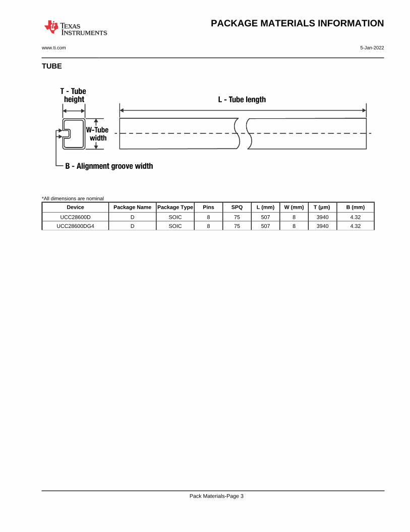
TUBE
*All dimensions are nominal
Device Package Name Package Type Pins SPQ L (mm) W (mm) T (µm) B (mm)
UCC28600D D SOIC 8 75 507 8 3940 4.32
UCC28600DG4 D SOIC 8 75 507 8 3940 4.32
PACKAGE MATERIALS INFORMATION
www.ti.com 5-Jan-2022
Pack Materials-Page 3
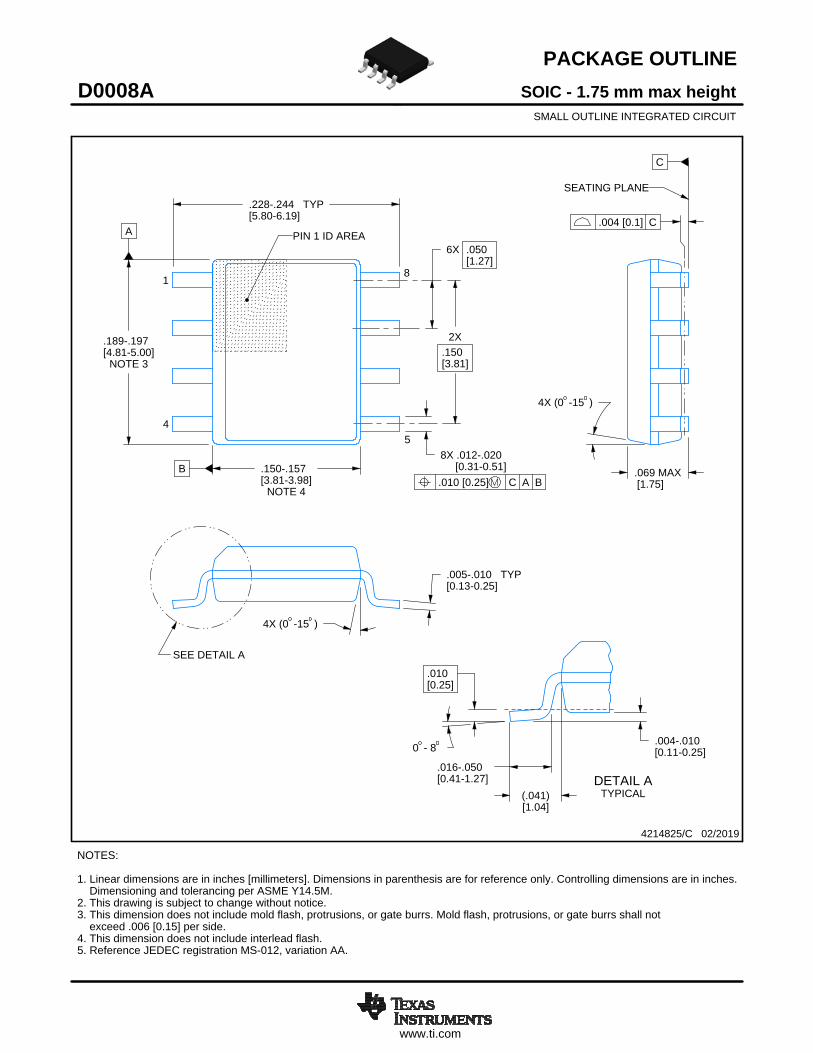
www.ti.com
PACKAGE OUTLINE
C
.228-.244 TYP[5.80-6.19]
.069 MAX[1.75]
6X .050[1.27]
8X .012-.020 [0.31-0.51]
2X.150[3.81]
.005-.010 TYP[0.13-0.25]
0 - 8 .004-.010[0.11-0.25]
.010[0.25]
.016-.050[0.41-1.27]
4X (0 -15 )
A
.189-.197[4.81-5.00]
NOTE 3
B .150-.157[3.81-3.98]
NOTE 4
4X (0 -15 )
(.041)[1.04]
SOIC - 1.75 mm max heightD0008ASMALL OUTLINE INTEGRATED CIRCUIT
4214825/C 02/2019
NOTES: 1. Linear dimensions are in inches [millimeters]. Dimensions in parenthesis are for reference only. Controlling dimensions are in inches. Dimensioning and tolerancing per ASME Y14.5M. 2. This drawing is subject to change without notice. 3. This dimension does not include mold flash, protrusions, or gate burrs. Mold flash, protrusions, or gate burrs shall not exceed .006 [0.15] per side. 4. This dimension does not include interlead flash.5. Reference JEDEC registration MS-012, variation AA.
18
.010 [0.25] C A B
54
PIN 1 ID AREA
SEATING PLANE
.004 [0.1] C
SEE DETAIL A
DETAIL ATYPICAL
SCALE 2.800
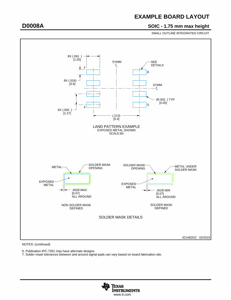
www.ti.com
EXAMPLE BOARD LAYOUT
.0028 MAX[0.07]ALL AROUND
.0028 MIN[0.07]ALL AROUND
(.213)[5.4]
6X (.050 )[1.27]
8X (.061 )[1.55]
8X (.024)[0.6]
(R.002 ) TYP[0.05]
SOIC - 1.75 mm max heightD0008ASMALL OUTLINE INTEGRATED CIRCUIT
4214825/C 02/2019
NOTES: (continued) 6. Publication IPC-7351 may have alternate designs. 7. Solder mask tolerances between and around signal pads can vary based on board fabrication site.
METALSOLDER MASKOPENING
NON SOLDER MASKDEFINED
SOLDER MASK DETAILS
EXPOSEDMETAL
OPENINGSOLDER MASK METAL UNDER
SOLDER MASK
SOLDER MASKDEFINED
EXPOSEDMETAL
LAND PATTERN EXAMPLEEXPOSED METAL SHOWN
SCALE:8X
SYMM
1
45
8
SEEDETAILS
SYMM
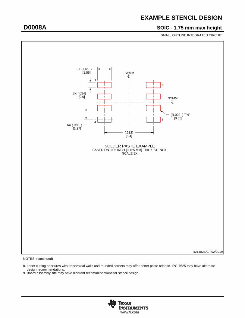
www.ti.com
EXAMPLE STENCIL DESIGN
8X (.061 )[1.55]
8X (.024)[0.6]
6X (.050 )[1.27]
(.213)[5.4]
(R.002 ) TYP[0.05]
SOIC - 1.75 mm max heightD0008ASMALL OUTLINE INTEGRATED CIRCUIT
4214825/C 02/2019
NOTES: (continued) 8. Laser cutting apertures with trapezoidal walls and rounded corners may offer better paste release. IPC-7525 may have alternate design recommendations. 9. Board assembly site may have different recommendations for stencil design.
SOLDER PASTE EXAMPLEBASED ON .005 INCH [0.125 MM] THICK STENCIL
SCALE:8X
SYMM
SYMM
1
45
8

IMPORTANT NOTICE AND DISCLAIMERTI PROVIDES TECHNICAL AND RELIABILITY DATA (INCLUDING DATA SHEETS), DESIGN RESOURCES (INCLUDING REFERENCE DESIGNS), APPLICATION OR OTHER DESIGN ADVICE, WEB TOOLS, SAFETY INFORMATION, AND OTHER RESOURCES “AS IS” AND WITH ALL FAULTS, AND DISCLAIMS ALL WARRANTIES, EXPRESS AND IMPLIED, INCLUDING WITHOUT LIMITATION ANY IMPLIED WARRANTIES OF MERCHANTABILITY, FITNESS FOR A PARTICULAR PURPOSE OR NON-INFRINGEMENT OF THIRD PARTY INTELLECTUAL PROPERTY RIGHTS.These resources are intended for skilled developers designing with TI products. You are solely responsible for (1) selecting the appropriate TI products for your application, (2) designing, validating and testing your application, and (3) ensuring your application meets applicable standards, and any other safety, security, regulatory or other requirements.These resources are subject to change without notice. TI grants you permission to use these resources only for development of an application that uses the TI products described in the resource. Other reproduction and display of these resources is prohibited. No license is granted to any other TI intellectual property right or to any third party intellectual property right. TI disclaims responsibility for, and you will fully indemnify TI and its representatives against, any claims, damages, costs, losses, and liabilities arising out of your use of these resources.TI’s products are provided subject to TI’s Terms of Sale or other applicable terms available either on ti.com or provided in conjunction with such TI products. TI’s provision of these resources does not expand or otherwise alter TI’s applicable warranties or warranty disclaimers for TI products.TI objects to and rejects any additional or different terms you may have proposed. IMPORTANT NOTICE
Mailing Address: Texas Instruments, Post Office Box 655303, Dallas, Texas 75265Copyright © 2022, Texas Instruments Incorporated