national aeronautics and space administration mil…€¦ · 13.06.2016 · 2016 electronics...
TRANSCRIPT
S. AgarwalNASA - Jet Propulsion Laboratory, California Institute of Technology
Pasadena, California, USA [email protected]
www.nasa.gov
National Aeronautics and Space Administration
GSFC, Greenbelt, Maryland June 13-16, 2016
Copyright 2016. All rights reserved..
MIL/JEDEC Standards Update
2016 Electronics Technology Workshop (ETW)
NASA Electronic Parts and Packaging Program (NEPP)
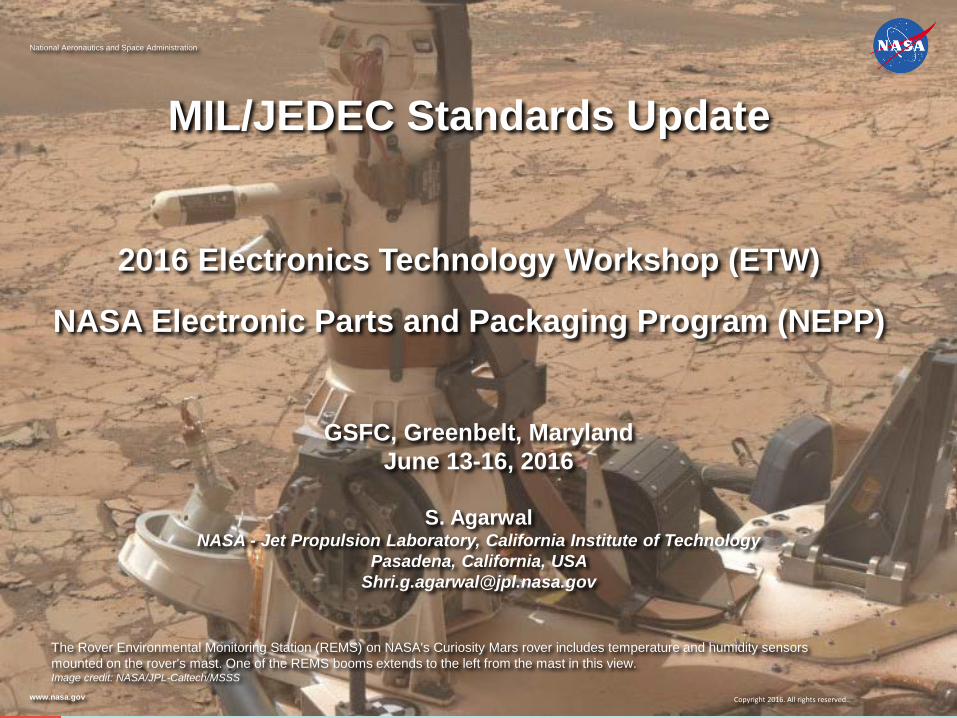
The Rover Environmental Monitoring Station (REMS) on NASA's Curiosity Mars rover includes temperature and humidity sensors mounted on the rover's mast. One of the REMS booms extends to the left from the mast in this view.Image credit: NASA/JPL-Caltech/MSSS
MIL/JEDEC standards play a vital role in electronic parts procurement and usage on all NASA missions. Through the NASA Electronic Parts Assurance Group (NEPAG) Program, NASA is an active participant in work related to the standards as they apply to electronic parts. This paper will provide an update on those activities.
Abstract
1
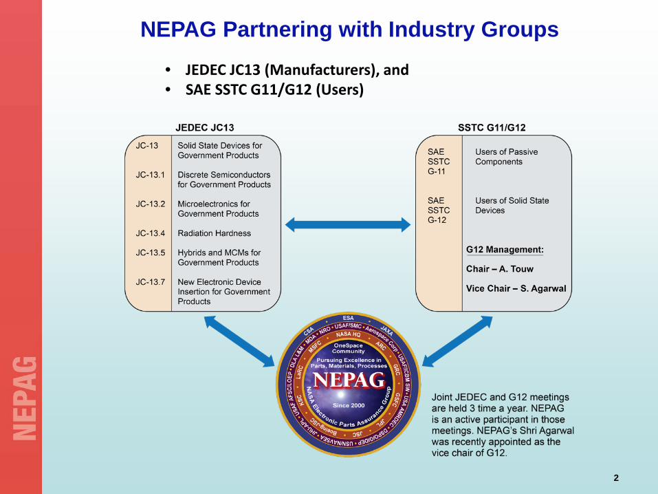
NEPAG Partnering with Industry Groups• JEDEC JC13 (Manufacturers), and• SAE SSTC G11/G12 (Users)
2

JEDEC/G11/G12 Meetingso JC13.x/G11/G12 Meetings
The JEDEC/G11/G12 meetings are held three times a year. The first meeting of FY16 was held in Jan 2016.
NASA participation:
Organize NEPAG meetings
Active involvement in Task Group meetings JC13.1, 13.2, 13.4, 13.5, 13.7, and G11/G12
G-12 & G11 Management Participate in Executive Council meetings as the G-12 Vice-chair, and
Chair of the G12 & G11 Space Subcommittee Take notes of G12 meetings Help with Task Group meetings
*JEDEC (Joint Electron Device Engineering Council) is a standardization body composed of semiconductor device manufacturers and their supply chains. SAE (Society of Automotive Engineers) coordinates development of technical standards by aerospace, automotive, and other users. Held three times a year, these meetings are key to parts standardization including the infusion of new technology
3

Grid for JEDEC/G11/G12 meetings (Example: Jan2016)
• NEPAG@JEDEC (circled above) is held to decide on member participation in JEDEC/G11/G12 meetings. 4
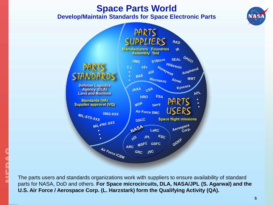
Space Parts WorldDevelop/Maintain Standards for Space Electronic Parts
The parts users and standards organizations work with suppliers to ensure availability of standard parts for NASA, DoD and others. For Space microcircuits, DLA, NASA/JPL (S. Agarwal) and the U.S. Air Force / Aerospace Corp. (L. Harzstark) form the Qualifying Activity (QA).
5
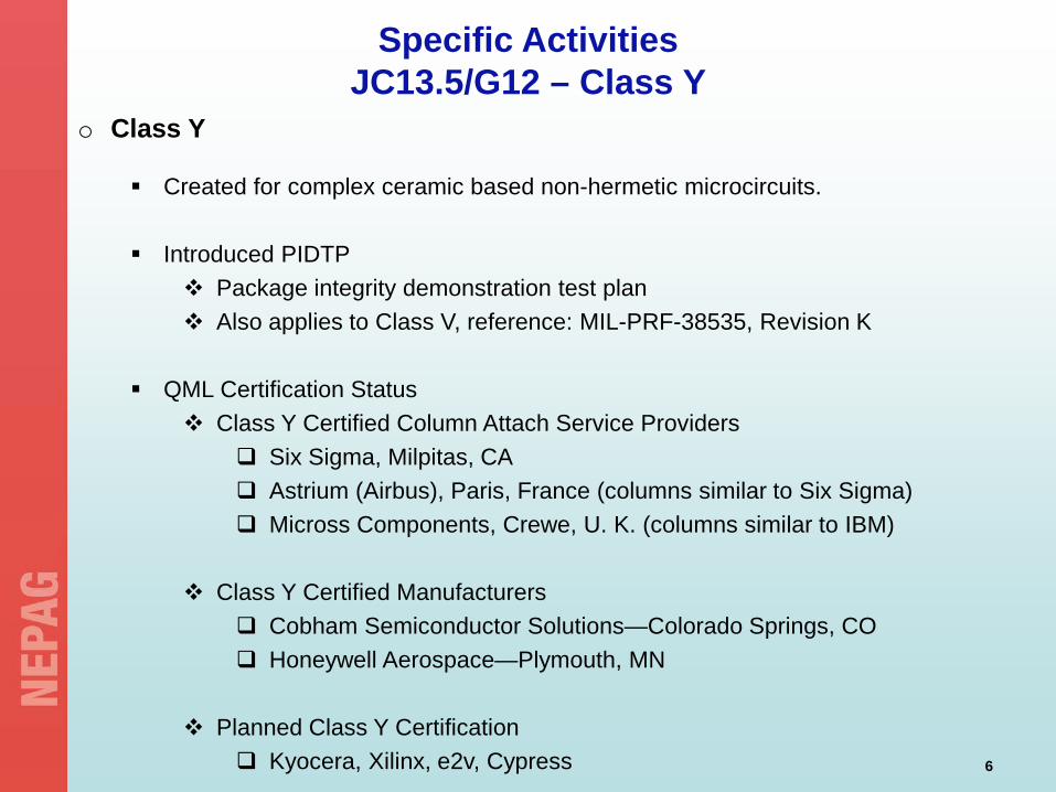
Specific ActivitiesJC13.5/G12 – Class Y
o Class Y
Created for complex ceramic based non-hermetic microcircuits.
Introduced PIDTP Package integrity demonstration test plan Also applies to Class V, reference: MIL-PRF-38535, Revision K
QML Certification Status Class Y Certified Column Attach Service Providers
Six Sigma, Milpitas, CA Astrium (Airbus), Paris, France (columns similar to Six Sigma) Micross Components, Crewe, U. K. (columns similar to IBM)
Class Y Certified Manufacturers Cobham Semiconductor Solutions—Colorado Springs, CO Honeywell Aerospace—Plymouth, MN
Planned Class Y Certification Kyocera, Xilinx, e2v, Cypress 6

G-12 Class Y
Task GroupNon-Hermetics in
Space
Manufacturers Primes
JC-13.2 Flip-chip Package BGA /
CGA** Requirements
Newly Formed Task Groups with Class Y Interest
JC-13.2 Electronic Parameters &
B.I. Standardization
JC-13/G-12/ G-11 BMEs
Task Group Activities Task Group Inputs
GovernmentReview M. Sampson Idea
Class Y ConceptDevelopment
EP Study (DLA-VA)
JC-13.25004/5 Testing BGA/CGA
w/balls?
Other Task Groups with Class Y Interest
G-12 Plastics Subcommittee
JC-13 TJ requirements
* PIDTP = Package Integrity Demonstration Test Plan** BGA / CGA = ball-grid array / column-grid array
Others
Users to procure QML-Y flight parts from certified/qualified suppliers
Manufacturer Certification to QML-Y (DLA-VQ)
Coordination Meeting at DLALand & Maritime (April 2012)
Aeroflex (October 2011)
Xilinx (February 2012)
Honeywell (May 2012)
Supplier PIDTP* Presentation
Minnowbrook ConferenceOct. 2013, New York
Conference
BAE (October 2012)
CMSE (2013, 2014), LA
e2v (January 2013)
DLA-VA to update 38535 with Class Y requirements and release the draft version (rev. K) for comments
DLA-VQ to begin preparation for auditing Class Y suppliers
DLA-VA to date 38535K
DLA-VQ to begin audit of suppliers to Class Y requirements
38535K CoordinationMeeting
Infusion of New Technology into Military StandardsNASA Led the Class Y Effort for Xilinx V4/V5 FPGAs and other similar Devices
Shows the Extent of Effort/Coordination
7

Specific ActivitiesJC13.4/G12 – Radiation Test Standard JESD57
o JESD57 Test Standard
Contains procedures for the measurement of single-event effects in semiconductor devices from heavy-ion irradiation.
Only U. S. test standard covering many of the heavy-ion induced single-event effects.
Last updated 20 years ago (in 1996) Does not reflect advanced electronics and complex technologies
A new revision will soon be submitted for a vote. NASA NEPP-led effort Point of contact: Jean-Marie Lauenstein
8
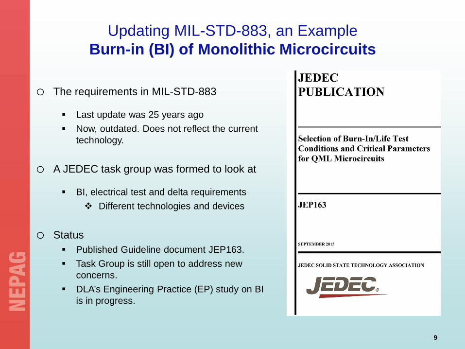
Updating MIL-STD-883, an ExampleBurn-in (BI) of Monolithic Microcircuits
o The requirements in MIL-STD-883
Last update was 25 years ago Now, outdated. Does not reflect the current
technology.
o A JEDEC task group was formed to look at
BI, electrical test and delta requirements Different technologies and devices
o Status Published Guideline document JEP163. Task Group is still open to address new
concerns. DLA’s Engineering Practice (EP) study on BI
is in progress.
9
Updating Requirements, an ExampleBI of Monolithic Microcircuits
o A New Concern
BI of high-speed devices What about hot spots on the die?
o Frequencies
500 MHz for digital functions A few giga-samples per second (Gsps) for data converters Several tens of gigahertz (GHz) for analog functions
o Status To be addressed in the Task Group
10

Dual Use Technology
• Basically an infusion of commercial monolithic microcircuits into DoD system.
o Rad hard by design 45nm CMOS microelectronics technology (BAE Systems, built at IBM foundry)
o Adding their unique processing steps to the existing processes, e.g. MRAMs being offered by Aeroflex and Honeywell (done in collaboration with Everspin)
o Upscreening selected products from commercial portfolio (Analog Devices)
• This has resulted in paradigm changes. An example follows:
o Not all parts are specified over the full military temperature range, –55°C to +125°C. Many of them call out –40°C to +110°C operating temperature range. These differences are now clearly shown in the standard microcircuit drawings (SMDs). However, there are no guidelines for BI of these devices. (Per notes 3/ and 4/ of the regression table, doing BI at temperatures lower than 125°C is not allowed for monolithic microcircuits.)
o It is unclear what assumptions went into generating the numbers.
11

MIL-STD-883, Test Method 1005
• Life test below 125°C not allowed for monolithic microcircuits.12

New Technology Flip-chip Deviceso Use of Underfills
The use of underfill material enhances reliability of flip-chip packages. MIL-PRF-38535K requires flip-chip devices to meet the underfill requirements specified in
MIL-STD-883, Test Method 5011. Several manufacturers are developing flip-chip products (Classes V and Y). It was
reported that there were problems in meeting the requirements in 5011. A JEDEC Task Group was formed to address this issue.
o Activities In order to bring the subject matter awareness, NASA published a special edition of EEE
Parts Bulletin on underfills. Defense Logistics Agency (DLA) conducted an Engineering Practice (EP) study Considerable discussion held in JEDEC meeting last week. Actions in progress are:
DLA to update the requirements, basically simplify them Review the revised requirements with manufacturers of flip-chip devices
o Status (monitored by S. Agarwal) A tentative plan developed to continue audits until the requirements in 5011 and/or 38535
are updated. The discussion will continue in Columbus, OH
1 hour allotted at the next JEDEC (September 2016) 13
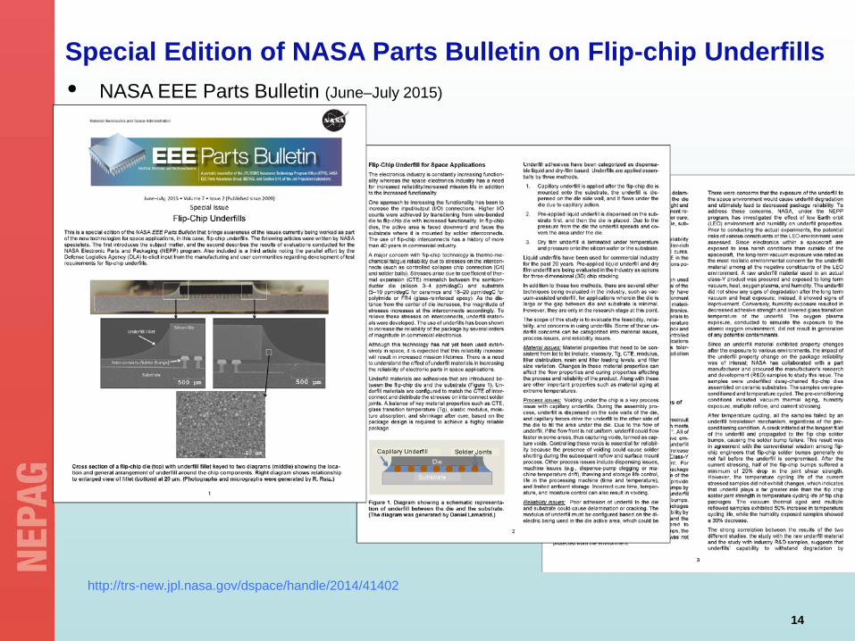
Special Edition of NASA Parts Bulletin on Flip-chip Underfills • NASA EEE Parts Bulletin (June–July 2015)
http://trs-new.jpl.nasa.gov/dspace/handle/2014/41402
14

G12 COTS (Commercial-Off-the-Shelf) EffortStandard PEMs (Plastic Encapsulated Microcircuits)
• NASA Applications Cubesats Smallsats
15
Signal Integrity Capacitors
o New technology high-speed devices require signal integrity capacitors
Commercial capacitors of base metal electrode (BME) construction were designed into the products Tiny, low voltage
o A task group comprised of the manufacturers and the users developed a screening specification
o Status The general specification MIL-PRF-32535 (formerly known as MIL-PRF-THIN)
and a set of 10 slash sheets were released few months back. MIL-PRF-38535 will be updated to include references to the MIL-PRF-32535.
The slash sheets for the interdigitated capacitors (IDCs), used in Xilinx Virtex 5 FPGAs and other new devices, are being worked.
16

New Issue (Presented at last week’s JEDEC/G12 Meeting)o Electro Static Discharge (ESD)
MIL-STD-883, Test Method 3015 Too old
Was written over 20 years ago Long test times (could be up to 5-6 hours per unit)
Needs to be revisited for new technology Smaller feature sizes, large number of pins, advancements in
packaging (2D, 3D) Resolve differences with latest JEDEC test methods
For example, 3015 requires 3 zaps, JEDEC requires 1 zap
MIL-PRF-38535 Clarify requirements
No specific ESD requirements for wafer foundries
NASA EEE Parts Bulletin Special edition on ESD being worked
NASA ESD Surveys To help the supply chain Bring general awareness
17

A New Trend – Supply Chain ManagementEnsuring gap-free alignment for each qualified product
(All entities in the supply chain must be certified/approved)
Company A Die design
Company B Wafer Fabrication
Company C Wafer Bumping
Company D Package design
Company E Assembly
Company F Column attach and solderability
Company G Screening
Company H Radiation testing
A Changing Landscape (Shipping/Handling/ESD Challenge)
18
Other Major Activities
o Leak rate and residual gas analysis (RGA)
o New technology insertion (>2D packaging)
o GaN, SiC Working Groups
o Hybrid element evaluation
o Passives
o Radiation hardness
o Plastic encapsulated microcircuit (PEM) screening and qual flows
o Copper bond wires qualification, testing
19
JPL’s main facility, at the foot of Southern California’s
San Gabriel Mountains.
Backup Slides
20
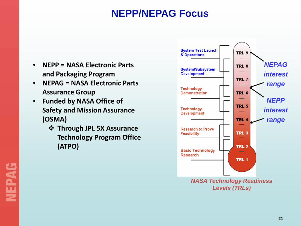
NASA Technology Readiness Levels (TRLs)
NEPPinterestrange
NEPAGinterestrange
NEPP/NEPAG Focus
• NEPP = NASA Electronic Parts and Packaging Program
• NEPAG = NASA Electronic Parts Assurance Group
• Funded by NASA Office of Safety and Mission Assurance (OSMA) Through JPL 5X Assurance
Technology Program Office (ATPO)
21
http://nepp.nasa.gov
ACKNOWLEDGMENTSThe research described in this publication was carried out, in part, at the Jet Propulsion Laboratory,California Institute of Technology, under a contract with the National Aeronautics and Space Administration.Help is gratefully acknowledged from J. Park, R. Carlson, and M. Sampson. Copyright 2016 California Institute of Technology. Government sponsorship acknowledged.
22