nanotechnology research in discovery park engineers led by david b. janes (electrical and computer...
Post on 21-Dec-2015
214 views
TRANSCRIPT
Nanotechnology Research in Discovery Park
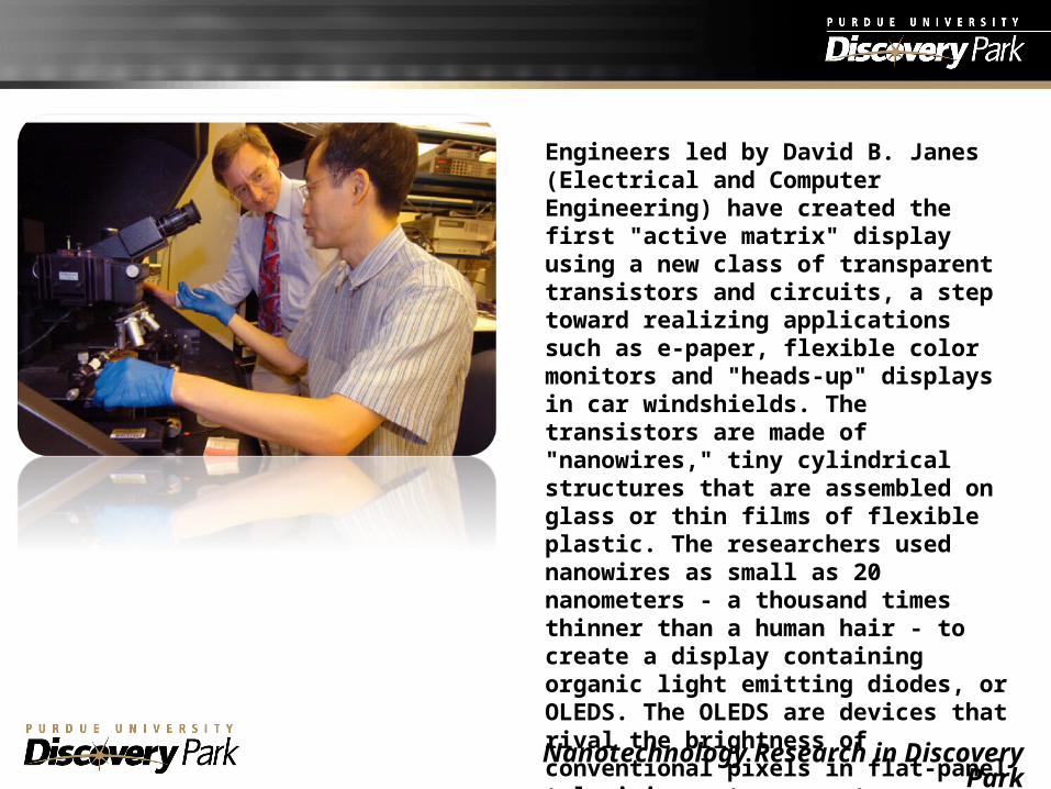
Engineers led by David B. Janes (Electrical and Computer Engineering) have created the first "active matrix" display using a new class of transparent transistors and circuits, a step toward realizing applications such as e-paper, flexible color monitors and "heads-up" displays in car windshields. The transistors are made of "nanowires," tiny cylindrical structures that are assembled on glass or thin films of flexible plastic. The researchers used nanowires as small as 20 nanometers - a thousand times thinner than a human hair - to create a display containing organic light emitting diodes, or OLEDS. The OLEDS are devices that rival the brightness of conventional pixels in flat-panel television sets, computer monitors and displays in consumer electronics.
Nanotechnology Research in Discovery Park
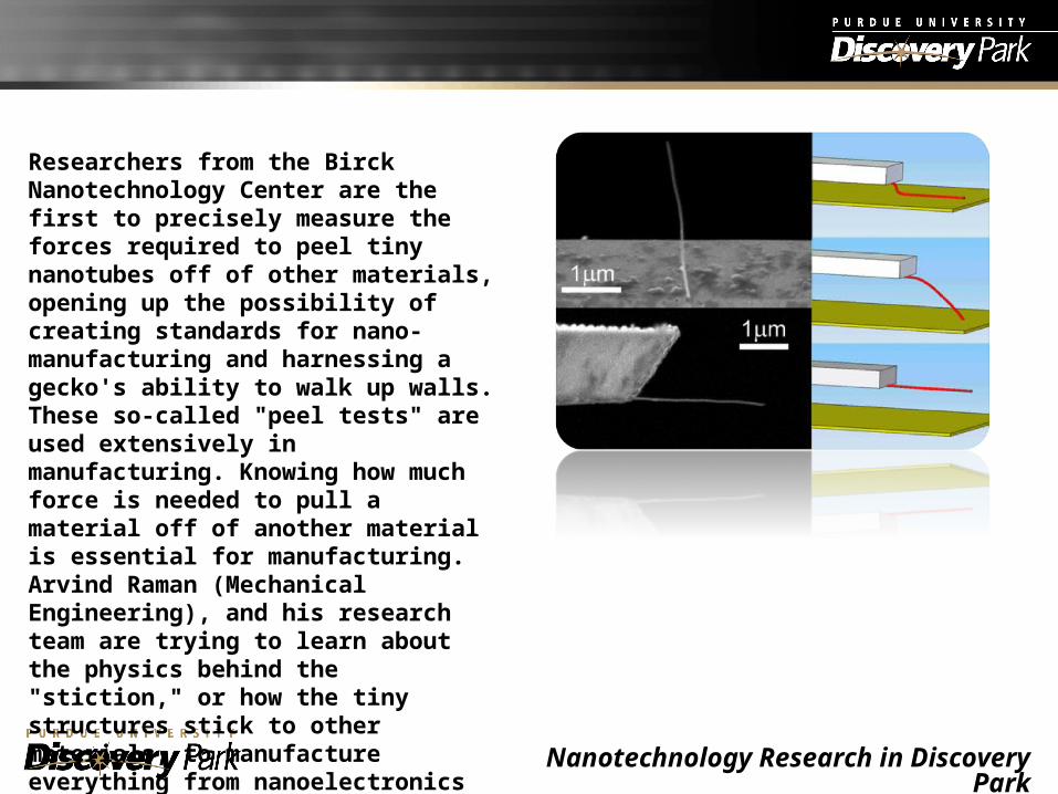
Researchers from the Birck Nanotechnology Center are the first to precisely measure the forces required to peel tiny nanotubes off of other materials, opening up the possibility of creating standards for nano-manufacturing and harnessing a gecko's ability to walk up walls. These so-called "peel tests" are used extensively in manufacturing. Knowing how much force is needed to pull a material off of another material is essential for manufacturing. Arvind Raman (Mechanical Engineering), and his research team are trying to learn about the physics behind the "stiction," or how the tiny structures stick to other materials, to manufacture everything from nanoelectronics to composite materials, "nanotweezers" to medical devices using nanotubes, nanowires and biopolymers such as DNA and proteins.

Nanotechnology Research in Discovery Park
“Solid-state lighting” based on light-emitting diodes, or LEDs, is a technology that is several times more efficient than conventional incandescent lights and more environmentally friendly than compact fluorescent bulbs. Timothy D. Sands (Materials Engineering and Electrical and Computer Engineering) and his collaborators are working on nanotechnology approaches to making LED lamps affordable. These LED lamps are expected to be far longer lasting than conventional lighting, perhaps lasting as long as 15 years before burning out. This lighting technology has the potential to cut electricity consumption by 10 percent if widely adopted.
Nanotechnology Research in Discovery Park
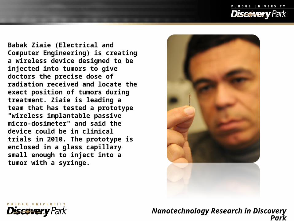
Babak Ziaie (Electrical and Computer Engineering) is creating a wireless device designed to be injected into tumors to give doctors the precise dose of radiation received and locate the exact position of tumors during treatment. Ziaie is leading a team that has tested a prototype "wireless implantable passive micro-dosimeter" and said the device could be in clinical trials in 2010. The prototype is enclosed in a glass capillary small enough to inject into a tumor with a syringe.

Nanotechnology Research in Discovery Park
“Optical cloaking” may one day become a reality thanks to research at the Birck Nanotechnology Center. Vladimir Shalaev (Electrical and Computer Engineering) and his research team have created a theoretical design that uses an array of tiny needles radiating outward from a central spoke. The design, which resembles a round hairbrush, would bend light around the object being cloaked. Background objects would be visible but not the object surrounded by the cylindrical array of nano-needles. Although this particular design would work only for one frequency, it still might have applications, such as producing a cloaking system to make soldiers invisible to night-vision goggles.

Chad Jafvert (Civil Engineering) suggests synthetic carbon molecules called fullerenes, or buckyballs, have a high potential of being accumulated in animal tissue, but the molecules also appear to break down in sunlight, perhaps reducing their possible environmental dangers. Buckyballs may see widespread use in future products and applications, from drug-delivery vehicles for cancer therapy to ultrahard coatings and military armor, chemical sensors and hydrogen-storage technologies for batteries and automotive fuel cells.
Nanotechnology Research in Discovery Park
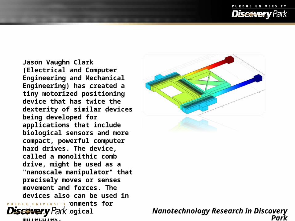
Jason Vaughn Clark (Electrical and Computer Engineering and Mechanical Engineering) has created a tiny motorized positioning device that has twice the dexterity of similar devices being developed for applications that include biological sensors and more compact, powerful computer hard drives. The device, called a monolithic comb drive, might be used as a "nanoscale manipulator" that precisely moves or senses movement and forces. The devices also can be used in watery environments for probing biological molecules.
Nanotechnology Research in Discovery Park
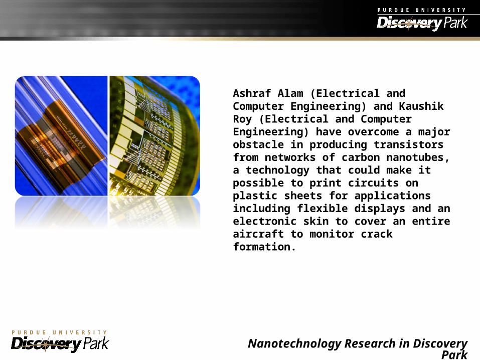
Ashraf Alam (Electrical and Computer Engineering) and Kaushik Roy (Electrical and Computer Engineering) have overcome a major obstacle in producing transistors from networks of carbon nanotubes, a technology that could make it possible to print circuits on plastic sheets for applications including flexible displays and an electronic skin to cover an entire aircraft to monitor crack formation.
Nanotechnology Research in Discovery Park
Nanotechnology Research in Discovery Park
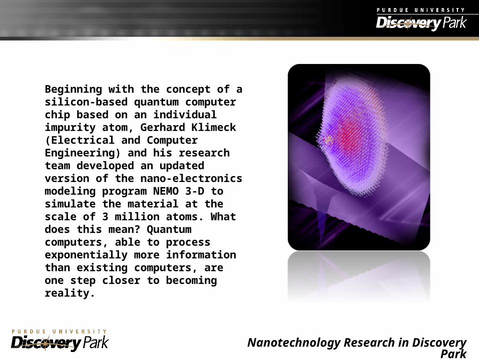
Beginning with the concept of a silicon-based quantum computer chip based on an individual impurity atom, Gerhard Klimeck (Electrical and Computer Engineering) and his research team developed an updated version of the nano-electronics modeling program NEMO 3-D to simulate the material at the scale of 3 million atoms. What does this mean? Quantum computers, able to process exponentially more information than existing computers, are one step closer to becoming reality.

Nanotechnology Research in Discovery Park
Researchers are developing a miniature refrigeration system small enough to fit inside laptops and personal computers, a cooling technology that would boost performance while shrinking the size of computers. Suresh Garimella (Mechanical Engineering) showed that unlike conventional cooling systems, which use a fan to circulate air through finned devices called heat sinks attached to computer chips, miniature refrigeration would dramatically increase how much heat could be removed.

Nanotechnology Research in Discovery Park
Engineers at the Birck Nanotechnology Center have shown how to grow forests of tiny cylinders called carbon nanotubes onto the surfaces of computer chips to enhance the flow of heat at a critical point where the chips connect to cooling devices called heat sinks. The carpetlike growth of nanotubes has been shown to outperform conventional "thermal interface materials." Like those materials, the nanotube layer does not require elaborate clean-room environments, representing a possible low-cost manufacturing approach to keep future chips from overheating and reduce the size of cooling systems.

Nanotechnology Research in Discovery Park
Masa Rao (Mechanical and Materials Engineering) researches micrometer-scale needles to ensure painless injection & fluid sampling. Potential applications involve improved glucose regulation for diabetes, transdermal drug delivery, novel cancer therapies, and electrodes for neural epiretinal prostheses.

Nanotechnology Research in Discovery Park
One feature of regenerative nanomedicine includes a cell-by-cell repair approach. Using self-assembling “programmable, multi-layered, MRI imagable, antibody or peptide-guided magnetic nanoparticles, James Leary (Basic Medical Sciences, and Biomedical Engineering) focuses on targeting cells for more precise drug/gene delivery systems. This approach includes manufacturing therapeutic genes inside a living cell using its own extra DNA and RNA precursors as raw materials and controlled by a molecular biosensor to deliver exactly the right amount of therapy to each cell.

Nanotechnology Research in Discovery Park
Researchers from IBM and Purdue University have discovered that tiny structures called silicon nanowires might be ideal for manufacturing in future computers and consumer electronics because they form the same way every time. The researchers used an instrument called a transmission electron microscope (TEM) to watch how nanowires made of silicon "nucleate," or begin to form, before growing into wires. Eric Stach’s (Materials Engineering) research team showed the nucleation process can be likened to the beginning of ice forming in a pool of water placed in a freezer. The liquid undergoes a "phase transition," changing from the liquid to the solid phase.

Researchers have created a precise biosensor for detecting blood glucose and potentially many other biological molecules by using hollow structures called single-wall carbon nanotubes anchored to gold-coated "nanocubes."
The device resembles a tiny cube-shaped tetherball. Each tetherball is a sensor and is anchored to electronic circuitry by a nanotube, which acts as both a tether and ultrathin wire to conduct electrical signals. Timothy Fisher (Mechanical Engineering), Marshall Porterfield (Agricultural and Biological Engineering) and graduate students said the technology, which detects glucose more precisely than any biosensors in development, also might be used in medicine to detect other types of biological molecules and in future biosensors for scientific research.
Nanotechnology Research in Discovery Park

These images were taken from a video illustrating a new technique that uses a laser and holograms to precisely position clusters of numerous tiny particles within seconds, representing a potential new tool to analyze biological samples or create devices using "nanoassembly." The red dots are individual particles. Researchers at the Birck Nanotechnology Center have developed a technique that uses a laser and holograms to precisely position numerous tiny particles within seconds, representing a potential new tool to analyze biological samples or create devices using nanoassembly. Steven T. Wereley’s (Mechanical Engineering) team used a technique, called rapid electrokinetic patterning, which is a potential alternative to existing technologies because the patterns can be more quickly and easily changed.
Nanotechnology Research in Discovery Park

Engineers at Purdue and Stanford universities have created stretchable electrodes to study how cardiac muscle cells, neurons and other cells react to mechanical stresses from heart attacks, traumatic brain injuries and other diseases.
The devices are made by injecting a liquid alloy made of indium and gallium into thin microchannels between two sheets of a plastic polymer. Babak Ziaie’s (Electrical and Computer Engineering) team designed a simple and cost-effective process for fabricating these stretchable platforms
Nanotechnology Research in Discovery Park