nano- and microlenses as concepts for enhanced performance
TRANSCRIPT

Nano- and microlenses as concepts forenhanced performance of solar cells
Martina SchmidPhillip Manley
Nano- and microlenses as concepts for enhancedperformance of solar cells
Martina Schmida,b,* and Phillip ManleyaaHelmholtz-Zentrum Berlin, Department of Renewable Energy, Nanooptical Concepts for PV,
Hahn-Meitner-Platz 1, 14109 Berlin, GermanybFreie Universität Berlin, Department of Physics, Arnimallee 14, 14195 Berlin, Germany
Abstract. Both metallic nanoparticles exhibiting plasmonic effects and dielectric nanoparticlescoupling the light into resonant modes have shown successful applications to photovoltaics.On a larger scale, microconcentrator optics promise to enhance solar cell efficiency and toreduce material consumption. Here, we want to create a link between the concentrators onthe nano- and on the microscale. From metallic nanospheres, we turn to dielectric ones andthen look at increasing radii to approach the microscale. The lenses are investigated with respectto their interaction with light using three-dimensional simulations with the finite-elementmethod. Resulting maps of local electric field distributions reveal the focusing behavior ofthe dielectric spheres. For larger lens sizes, ray tracing calculations, which give ray distributionsin agreement with electric field intensities, can be applied. Calculations of back focal lengths ingeometrical optics coincide with ray tracing results and allow insight into how the focal lengthcan be tuned as a function of particle size, substrate refractive index, and the shape of the micro-lens. Despite the similarities we find for the nano- and the microlenses, integration into solarcells needs to be carefully adjusted, depending on the goals of material saving, concentrationlevel, focal distance, and lens size. © 2015 Society of Photo-Optical Instrumentation Engineers (SPIE)[DOI: 10.1117/1.JPE.5.057003]
Keywords: light coupling; plasmonics; nanosphere; microlens; concentration; focal length; raytracing; solar cell.
Paper 14043SSP received Jul. 18, 2014; revised manuscript received Oct. 10, 2014; accepted forpublication Oct. 15, 2014; published online Nov. 25, 2014.
1 Introduction
Plasmonic absorption enhancement by metal nanoparticles has been identified as a promisingconcept for boosting solar cell efficiency.1 High angle scattering, enhanced near-fields and, in thecase of regular particle arrangements, coupling into guided modes are the main mechanismsidentified to improve light absorption.2 As a result, plasmonic nanoparticles have been studiedfor various types of solar cells, such as silicon,3 organic,4 dye-sensitized, GaAs, and recentlychalcopyrite-based ones.5 Another approach for light trapping, dielectric nanoparticles, is aresult of the search for increased efficiency, but also offers an easy and stable integrationinto the solar cell. Related effects of light coupling can be attributed to whispering gallerymodes,6 but general anti-reflection effects also play a fundamental role.7 Compared to theirmetallic counterparts, dielectric nanoparticles may show equally strong scattering behavior,yet without any related absorption losses. However, they may lose in terms of high anglescattering, yet exhibit a strong forward scattering.8 First, we will briefly revisit near-fields aroundmetallic and dielectric nanospheres, and then turn to dielectric spheres of increasing size whichshow a progressive trend toward a defined focal spot.
Micrometer-sized dielectric spheres have been identified to give rise to so-called photonicnanojets, which were identified early to have the potential for a novel ultramicroscopy tech-nique.9 Detailed studies of the nanojet evolution as a function of parameters such as wavelength,
*Address all correspondence to: Martina Schmid, E-mail: [email protected]
0091-3286/2015/$25.00 © 2015 SPIE
Journal of Photonics for Energy 057003-1 Vol. 5, 2015

particle size and refractive index of sphere, and surrounding have followed.10,11 In this paper,we want to focus on the similarity of light concentration behind dielectric particles and thewell-known focusing behavior of lenses. We will show how the focus of the nanojets can beequally described by ray tracing methods as well as in geometrical optics calculations forlight propagation through a lens for the case of microspheres large compared to the wavelength.The transition to plano-convex lenses will be highlighted since this relates to the particularapplication in solar cells which has recently attracted attention: microconcentrator solarcells. In this concept, the sunlight is concentrated by micro-optics onto micrometer-sizedsolar cells for the purpose of material saving and efficiency enhancement.12,13 This reducesthe well-known concept of concentrator photovoltaics14 to the micrometer scale in order tofabricate compact high efficiency devices. Since commonly available lens arrays are often char-acterized by segment-like shapes, we will address shape effects as well as the influence ofthe substrate’s refractive index.
By establishing the link between the nanoscaled metallic and dielectric particle concentratorson one hand, and the lens-like microconcentrators on the other hand, we aim at providinga unified picture of the different aspects of light concentration for efficiency enhancement,particularly in photovoltaic devices. These two different aspects may be classified as follows:(1) Absorption enhancement by locally enhanced near-fields, preferential forward and high anglescattering for improved incoupling and prolonged optical path lengths. This aspect will lead to an
increased short-circuit current density jsc with an upper limit given by jsc;max ¼ ∫ λg0
AM1.5ðλÞ·λh·c dλ.
(2) Increased photon flux density by concentrating the incoming light from an area A0 to Acell
with a concentration factor of C ¼ A0∕Acell. This effect can lead to a maximum short-circuit
current density jsc;max ¼ ∫ λg0 C · AM1.5ðλÞ·λ
h·c dλ, and the open-circuit voltage Voc is enhanced
according to Voc ∝ lnðC·jscj0Þ.15 Going from (1) to (2) requires a reduced device area for maximum
benefit and we will find the lens sizes where this becomes relevant.
2 Approach and Computational Methods
The modification of light propagation by nano- and micrometer-sized spheres, hemispheres, andplano-convex lenses is investigated. We start with a comparison of small metallic (Ag) versusdielectric (SiO2) nanospheres, and then focus on the dielectric case when investigating increasingsizes and various shapes. Ag refractive index data are interpolated to 0.14221þ 4.52296 iaccording to the data from Ref. 16, whereas the refractive index for SiO2 is set ton ¼ 1.53839 (according to Ref. 17) for the wavelength λ ¼ 700 nm investigated here. Wefocus on this wavelength due to its significance for the application to chalcopyrite solarcells with reduced absorber thickness, which requires an absorption enhancement in therange starting from this wavelength. Chalcopyrites, or CuðIn;GaÞSe2 (CIGSe) compounds,are used as absorber materials in thin-film solar cells due to their direct band gap and resultinggood efficiencies. But they also come with the aim of reducing material consumption sincethey contain the rare element indium. When thinking about the application of concentratorlenses to this type of solar cells, the refractive indices of the absorber layer, which is approx-imately 2.8, and that of the front contact ZnO:Al, which is approximately 1.8, are of interest.We will exemplarily use them when assigning particular refractive indices to substrates later on.The imaginary part of the refractive index will be kept to zero in order to follow the lightpropagation. For investigating the intensity distributions and focusing effects of the nano-and microlenses, three approaches are followed: three-dimensional (3-D) optical simulationsusing the finite-element method (FEM), ray tracing, and geometrical optics calculations. TheFEM and ray tracing are briefly described in the following, whereas Sec. 3 is dedicated tothe geometrical optics calculations. The generalized structure of the shapes can be seen inFig. 1 as used for the geometrical optics calculations.
The 3-D optical simulations are carried out using the software package JCMsuite.18,19 It isbased on the FEM, i.e., the computational domain is divided into geometrical primitives with adiscretization adaptable to the particular geometry. Using local polynomial functions, the sol-ution space to Maxwell’s equations in the time–harmonic ansatz for the entire domain can be
Schmid and Manley: Nano- and microlenses as concepts for enhanced performance of solar cells
Journal of Photonics for Energy 057003-2 Vol. 5, 2015

approximated. In the examples presented here, the cylindrical symmetry of the geometry hasbeen exploited to reduce the computational effort. This allows the solutions to Maxwell’s equa-tions to be expanded in a Fourier basis, which accounts for the angular dependence.20 The com-putational domain was terminated by perfectly matched layer (PML) boundary conditions. Thetotal electric field surrounding the particle was calculated. Due to the memory requirements ofthe FEM, a computational domain size which is larger than a few tens of wavelengths becomescostly, even when exploiting the cylindrical symmetry as explained above. This meant that forour chosen wavelength of 700 nm, calculations for particle diameters larger than 10,000 nmbecame very time consuming using the FEM. Accordingly, near-field pictures shown inthe following represent the electric field distribution normalized to the incoming field jEj∕jE0jdisplayed in the xz-plane at y ¼ 0; the z-direction is defined as the negative propagation direc-tion of the incident light with polarization along the x-direction.
Sequential ray tracing describes the propagation of light rays when traveling from an objectto an image plane via a given sequence of surfaces. At each of the surfaces, the ray propagation isdescribed according to the laws of reflection and refraction and no paraxial approximation ismade. By following the path of a ray, its angle of incidence onto an optical surface can be iden-tified and Snell’s law accordingly applied. Ray tracing is mostly used for the design of opticalelements and systems and this is very suitable for our investigations of micrometer-sized lenses,where near-field effects are negligible. For the calculations shown here, we used the softwareRadiant Zemax, Version 13.21
3 Geometrical Optics Calculations
Geometrical optics or ray optics can be used to describe light propagation through media andobjects much larger than the wavelength. Based on this approach, we investigate the rear focallength f and the back focal length (BFL) for a generalized structure of a lens as depicted inFig. 1. The lens is defined by two curved surfaces with radii r1 and r2 and a total thicknessof d and has a refractive index of n2; it is embedded in an incoming medium with n1 andan outgoing medium with n3, eventually on top of a substrate with n4.
Details of the derivation are given in Ref. 22. Here, we only summarize the results which arethe Generalized Lensmaker’s equation:
1
f¼ n2 − n1
n4·1
r1−n2 − n3
n4·1
r2þ ðn2 − n1Þ · ðn2 − n3Þ
n2 · n4·
dr1 · r2
; (1)
and the back focal length
BFL ¼ f ·
�1 −
n2 − n1n2
·dr1
�: (2)
Fig. 1 Schematic of a generalized lens structure defined by two curved surfaces with radii r 1 andr 2 and a total thickness of d with the lens having a refractive index of n2 while being embedded inan incoming medium with n1 and an outgoing medium with n3, eventually also on top of a substratewith n4.
Schmid and Manley: Nano- and microlenses as concepts for enhanced performance of solar cells
Journal of Photonics for Energy 057003-3 Vol. 5, 2015

The particular shapes investigated are spheres, hemispheres and circular segments in air andon a substrate. The spherical elements are described by the radius r and the segments by thesegment width s and the height h, resulting in r ¼ ð4 h2 þ s2Þ∕ð8 hÞ for the latter ones. Withthe definition of the height as a certain ratio of the segment width this can be expressed as
rsegment ¼s · ð4 · ratio2 þ 1Þ
8 · ratiofor h ¼ ratio · s (3)
The resulting equations for the rear focal length and the BFL for the various cases are sum-marized in Table 1.
4 Results and Discussions
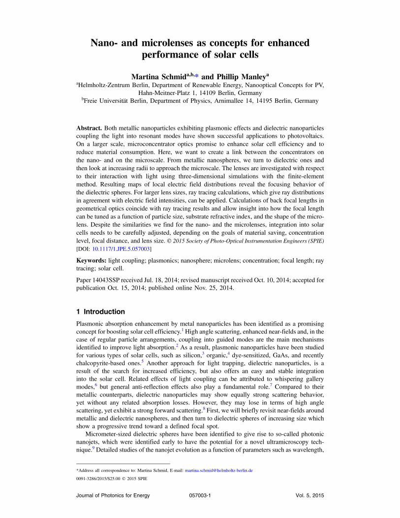
Looking at spheres on the nanoscale, a strong near-field enhancement is one of the reasons thatmetallic nanoparticles are of interest for absorption enhancement. Figure 2(a) shows the normal-ized electric near-field distribution (calculated with FEM) around a Ag nanoparticle with r ¼200 nm at a wavelength of 700 nm. The representation is a cut through the xz-plane at y ¼ 0
with polarization along the (horizontal) x-direction and the k-vector along the negative z-direc-tion. It clearly reveals a high concentration of the field around the boundary of the metallicnanoparticle, which is due to the free charge carriers repelling fields from inside the nanoparticle.Additionally, the lobes of this quadrupole mode are visible, highlighting the second benefit ofplasmonic nanoparticles, namely the reradiation of light into high angles, potentially leading tolight trapping in an underlying layer. Despite these benefits, metallic nanoparticles may alsoshow parasitic absorption resulting in losses in the form of heat. This disadvantage togetherwith the challenge of stable integration into solar cells23 leads to the consideration of nanopar-ticles made from dielectric materials, which can equally show high scattering ability with similarresonance wavelengths for slightly larger sizes. A detailed comparison of metallic versus dielec-tric nanoparticles was conducted in Ref. 8. Here, we focus on the very particular electric fielddistribution around dielectric nanoparticles as shown in Fig. 2(b) for the example of a SiO2
nanosphere with r ¼ 300 nm. The light is preferentially guided to the forward direction andconcentrated in the shadow region behind the nanoparticle. This focusing effect, already
Table 1 Formulas for the rear focal length and the back focal length (BFL) for spheres,hemispheres, and segments in air and on a substrate according to the generalized lensmaker’sequation, Eq. (1) and the equation for the BFL, Eq. (2).
Configuration Focal length Back focal length
Sphere of radius r ¼ r 1 ¼ −r 2 with refractiveindex n ¼ n2 in air (n1 ¼ n3 ¼ n4 ¼ 1); d ¼ 2r
1f ¼ n−1
n · 2r BFL ¼ f · 2−nn ¼ 2−n2ðn−1Þ · r
Sphere of radius r with refractive indexn2 ¼ n in air (n1 ¼ n3 ¼ 1), but ona substrate with n4 ¼ nsubs
1f ¼ n−1
n·nsubs· 2r BFL ¼ f · 2−nn ¼ ð2−nÞ·nsubs
2ðn−1Þ · r
Hemisphere of radius r ¼ r 1 ¼ d , r 2 ¼ ∞with refractive index n ¼ n2 in air(n1 ¼ n3 ¼ n4 ¼ 1)
1f ¼ ðn − 1Þ · 1r BFL ¼ f · 1n ¼ 1
nðn−1Þ · r
Hemisphere of radius r with refractiveindex n2 ¼ n in air (n1 ¼ n3 ¼ 1), but ona substrate with n4 ¼ nsubs
1f ¼ n−1
nsubs· 1r BFL ¼ f · 1n ¼ nsubs
nðn−1Þ · r
Segment of width s, height h ¼ s · ratio ¼ d ,radius r according to Eq. (3) and with refractiveindex n ¼ n2 in air (n1 ¼ n3 ¼ n4 ¼ 1)
1f ¼ ðn − 1Þ · 1r BFL ¼ f · ð1 − n−1
n · hr Þ ¼ 1n−1 · r −
1n · h
Segment of width s, height h ¼ s · ratio,radius r and with refractive index n2 ¼ n in air(n1 ¼ n3 ¼ 1), but on a substrate with n4 ¼ nsubs
1f ¼ n−1
nsubs· 1r BFL ¼ f · ð1 − n−1
n · hr Þ ¼ nsubsn−1 · r − nsubs
n · h
Schmid and Manley: Nano- and microlenses as concepts for enhanced performance of solar cells
Journal of Photonics for Energy 057003-4 Vol. 5, 2015
observable for dielectric particles smaller than the wavelength, will be a center point of ourdiscussion as we proceed to larger sphere sizes.
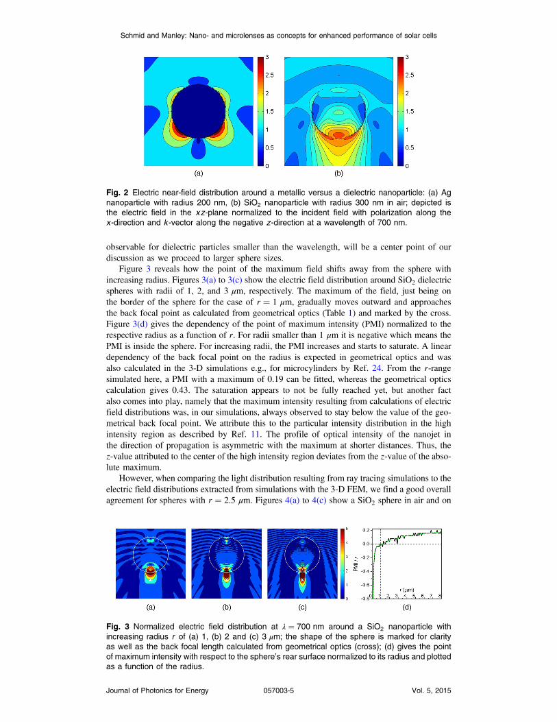
Figure 3 reveals how the point of the maximum field shifts away from the sphere withincreasing radius. Figures 3(a) to 3(c) show the electric field distribution around SiO2 dielectricspheres with radii of 1, 2, and 3 μm, respectively. The maximum of the field, just being onthe border of the sphere for the case of r ¼ 1 μm, gradually moves outward and approachesthe back focal point as calculated from geometrical optics (Table 1) and marked by the cross.Figure 3(d) gives the dependency of the point of maximum intensity (PMI) normalized to therespective radius as a function of r. For radii smaller than 1 μm it is negative which means thePMI is inside the sphere. For increasing radii, the PMI increases and starts to saturate. A lineardependency of the back focal point on the radius is expected in geometrical optics and wasalso calculated in the 3-D simulations e.g., for microcylinders by Ref. 24. From the r-rangesimulated here, a PMI with a maximum of 0.19 can be fitted, whereas the geometrical opticscalculation gives 0.43. The saturation appears to not be fully reached yet, but another factalso comes into play, namely that the maximum intensity resulting from calculations of electricfield distributions was, in our simulations, always observed to stay below the value of the geo-metrical back focal point. We attribute this to the particular intensity distribution in the highintensity region as described by Ref. 11. The profile of optical intensity of the nanojet inthe direction of propagation is asymmetric with the maximum at shorter distances. Thus, thez-value attributed to the center of the high intensity region deviates from the z-value of the abso-lute maximum.
However, when comparing the light distribution resulting from ray tracing simulations to theelectric field distributions extracted from simulations with the 3-D FEM, we find a good overallagreement for spheres with r ¼ 2.5 μm. Figures 4(a) to 4(c) show a SiO2 sphere in air and on
Fig. 2 Electric near-field distribution around a metallic versus a dielectric nanoparticle: (a) Agnanoparticle with radius 200 nm, (b) SiO2 nanoparticle with radius 300 nm in air; depicted isthe electric field in the xz-plane normalized to the incident field with polarization along thex -direction and k -vector along the negative z-direction at a wavelength of 700 nm.
Fig. 3 Normalized electric field distribution at λ ¼ 700 nm around a SiO2 nanoparticle withincreasing radius r of (a) 1, (b) 2 and (c) 3 μm; the shape of the sphere is marked for clarityas well as the back focal length calculated from geometrical optics (cross); (d) gives the pointof maximum intensity with respect to the sphere’s rear surface normalized to its radius and plottedas a function of the radius.
Schmid and Manley: Nano- and microlenses as concepts for enhanced performance of solar cells
Journal of Photonics for Energy 057003-5 Vol. 5, 2015
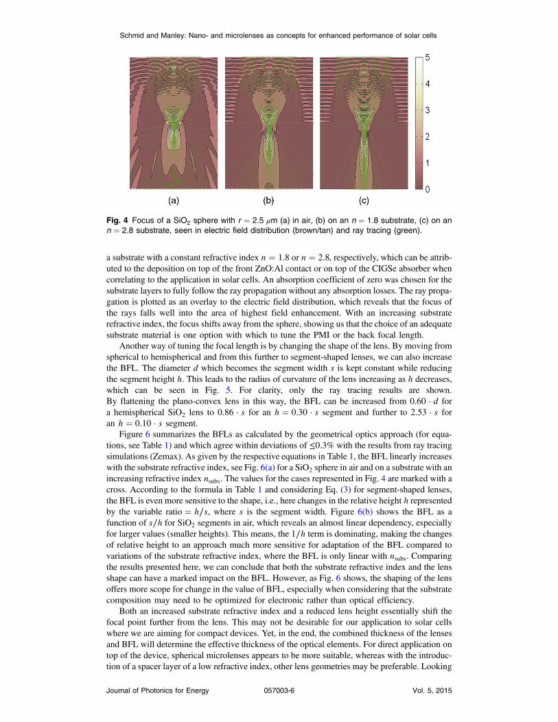
a substrate with a constant refractive index n ¼ 1.8 or n ¼ 2.8, respectively, which can be attrib-uted to the deposition on top of the front ZnO:Al contact or on top of the CIGSe absorber whencorrelating to the application in solar cells. An absorption coefficient of zero was chosen for thesubstrate layers to fully follow the ray propagation without any absorption losses. The ray propa-gation is plotted as an overlay to the electric field distribution, which reveals that the focus ofthe rays falls well into the area of highest field enhancement. With an increasing substraterefractive index, the focus shifts away from the sphere, showing us that the choice of an adequatesubstrate material is one option with which to tune the PMI or the back focal length.
Another way of tuning the focal length is by changing the shape of the lens. By moving fromspherical to hemispherical and from this further to segment-shaped lenses, we can also increasethe BFL. The diameter d which becomes the segment width s is kept constant while reducingthe segment height h. This leads to the radius of curvature of the lens increasing as h decreases,which can be seen in Fig. 5. For clarity, only the ray tracing results are shown.By flattening the plano-convex lens in this way, the BFL can be increased from 0.60 · d fora hemispherical SiO2 lens to 0.86 · s for an h ¼ 0.30 · s segment and further to 2.53 · s foran h ¼ 0.10 · s segment.
Figure 6 summarizes the BFLs as calculated by the geometrical optics approach (for equa-tions, see Table 1) and which agree within deviations of ≤0.3% with the results from ray tracingsimulations (Zemax). As given by the respective equations in Table 1, the BFL linearly increaseswith the substrate refractive index, see Fig. 6(a) for a SiO2 sphere in air and on a substrate with anincreasing refractive index nsubs. The values for the cases represented in Fig. 4 are marked with across. According to the formula in Table 1 and considering Eq. (3) for segment-shaped lenses,the BFL is even more sensitive to the shape, i.e., here changes in the relative height h representedby the variable ratio ¼ h∕s, where s is the segment width. Figure 6(b) shows the BFL as afunction of s∕h for SiO2 segments in air, which reveals an almost linear dependency, especiallyfor larger values (smaller heights). This means, the 1∕h term is dominating, making the changesof relative height to an approach much more sensitive for adaptation of the BFL compared tovariations of the substrate refractive index, where the BFL is only linear with nsubs. Comparingthe results presented here, we can conclude that both the substrate refractive index and the lensshape can have a marked impact on the BFL. However, as Fig. 6 shows, the shaping of the lensoffers more scope for change in the value of BFL, especially when considering that the substratecomposition may need to be optimized for electronic rather than optical efficiency.
Both an increased substrate refractive index and a reduced lens height essentially shift thefocal point further from the lens. This may not be desirable for our application to solar cellswhere we are aiming for compact devices. Yet, in the end, the combined thickness of the lensesand BFL will determine the effective thickness of the optical elements. For direct application ontop of the device, spherical microlenses appears to be more suitable, whereas with the introduc-tion of a spacer layer of a low refractive index, other lens geometries may be preferable. Looking
Fig. 4 Focus of a SiO2 sphere with r ¼ 2.5 μm (a) in air, (b) on an n ¼ 1.8 substrate, (c) on ann ¼ 2.8 substrate, seen in electric field distribution (brown/tan) and ray tracing (green).
Schmid and Manley: Nano- and microlenses as concepts for enhanced performance of solar cells
Journal of Photonics for Energy 057003-6 Vol. 5, 2015

at the influence of overall lens size, even for a substrate index of n ¼ 1.5, i.e., glass, and aspherical lens made from SiO2, the BFL in the case of a 500-μm diameter lens isBFL ¼ 320 μm. For a 500 times smaller SiO2 spherical lens with d ¼ 1 μm, the BFL in an n ¼1.5 substrate layer was only BFL ¼ 0.64 μm. Therefore, for spherical lenses, additional spacerlayers may also be desirable with increasing lens size.
For a detailed analysis of light concentration as a function of sphere sizes, we go back to thelocal distributions of the electric field intensities. Figure 7 compares the horizontal intensityprofiles ðjEj∕jE0jÞ2 at y ¼ 0 and a distance z ¼ 0, i.e., at the interface between air and an n ¼1.8material on top of which SiO2 spheres with different radii are located. Behind the r ¼ 0.3 μmsphere, a broad intensity distribution over the whole lens area is found (black curve), whichalready shows an increase compared with the basic transmittance expected at the interface with-out spheres (dashed orange line which corresponds to a transmittance of 91.8%). The red curvefor an r ¼ 0.9 μm and the green curve for an r ¼ 2.7 μm sphere show how the maximum inten-sity increases and the peak narrows with increasing lens radius. The diameters of the lenses from
Fig. 5 Increasing back focal length of plano-convex lens made from SiO2 with decreasing heightand increasing radius of curvature. The height is given as a ratio of the segment width with ratio ¼(a) 0.5 (hemisphere), (b) 0.4, (c) 0.3 and (d) 0.2.
Fig. 6 Back focal length (according to Table 1 for geometrical optics calculations which agree withresults from ray tracing simulations) for (a) a SiO2 sphere in air and on a substrate and (b) SiO2
hemispheres and segments in air; the total curve progressions are shown with marks for theparticular cases represented in Figs. 4 and 5 (s or 2 · r set to 1).
Schmid and Manley: Nano- and microlenses as concepts for enhanced performance of solar cells
Journal of Photonics for Energy 057003-7 Vol. 5, 2015

which the peaks arise are indicated by the bars on top of the graph (colors correspond to solidcurves). The full width at half maximum for the case r ¼ 0.9 μm, for which the PMI starts to belocated outside the sphere, is 0.40 · d, while for a three times larger lens (r ¼ 2.7 μm), it hasnarrowed down to 0.24 · d. The blue curve represents the line scan along the x-axis atz ¼ −0.54 μm, i.e., at the distance of the PMI, for the case of an r ¼ 2.7 μm sphere, whichshows a further increase in intensity and a reduction in width. (Annotation: the dip at x ¼ 0
of the intensity profiles is attributed to a simulation artifact of the sphere touching the substrateat a singular point only; however, this does not change the trends described.)
Next, we consider a chalcopyrite solar cell placed directly beneath the three differently sizeddielectric spheres. The radius of the cylindrical solar cell was set to the radius of the smallestsphere, i.e., 0.3 μm and the solar cell structure was ZnO∶Al∕i-ZnO∕CdS∕CuðIn;GaÞSe2∕Mo
(top to bottom on glass substrate) with thicknesses 100/50/50/500/200 nm, respectively.Underneath the solar cell is a glass substrate which extended over the entire width of the domain.The simulations were carried out with the FEM and using the previously described cylindricalcoordinate system. PML layers were used in all outgoing directions. For each lens radius, theamount of light absorbed in the chalcopyrite layer was calculated. The usual normalization forthis absorption would be the total energy which was incident to the computational domain.However, since the system is isolated, such a normalization would cause the absorption tobe dependent on the domain size. To try and avoid this dependence, we have normalizedthe amount of energy absorbed by the chalcopyrite layer to the amount of energy incidentto either the lens or to the solar cell in the ray optics regime. The value of the absorption nor-malized to the lens area, AL, is 2.42, 1.11, and 0.80 for the 0.3, 0.9, and 2.7 μm radius lens,respectively. Because we have normalized the amount of energy directly incident to the lens, thefirst two values are larger than 1.0. By looking at the Poynting flux lines in Figs. 8(a) and 8(b),we can see that flux lines which begin outside of the radius of the lens penetrate into the chal-copyrite layer, meaning that more light may be absorbed than was directly incident to the lens.For the largest lens, only energy flux lines which were originally incident to the lens penetratethe chalcopyrite layer. This means that for sub-wavelength-sized lenses, the lenses would notneed to be closely packed to ensure the maximum absorption in the solar cell. For all lens sizes,the solar cell suffers from some parasitic absorption in the window, buffer, and back contactlayer. Further, the largest lens suffers from imperfect focusing, which may be improved by posi-tioning the solar cell so that the chalcopyrite layer is at the focal position.
If we look now at the absorption normalized to the solar cell area, ASC, the values are 2.42,10.01, and 64.40 for the 0.3, 0.9, and 2.7 μm radius lenses, respectively, see the comparison inTable 2. This factor relates to the concentration of light. If the entire energy incident to the lenswas absorbed in the chalcopyrite layer, then the ratio of the lens and solar cell area would give usthe absorbed energy, which for the sizes presented would be 1, 9, and 81. The smaller two lenses
Fig. 7 Intensity profiles at y ¼ 0 at the interface (z ¼ 0) of air and an n ¼ 1.8 material on top ofwhich SiO2 spheres with sizes as given are located. The bars on the top give the diameter ofthe lenses from which the peaks arise (colors correspond to curves).
Schmid and Manley: Nano- and microlenses as concepts for enhanced performance of solar cells
Journal of Photonics for Energy 057003-8 Vol. 5, 2015
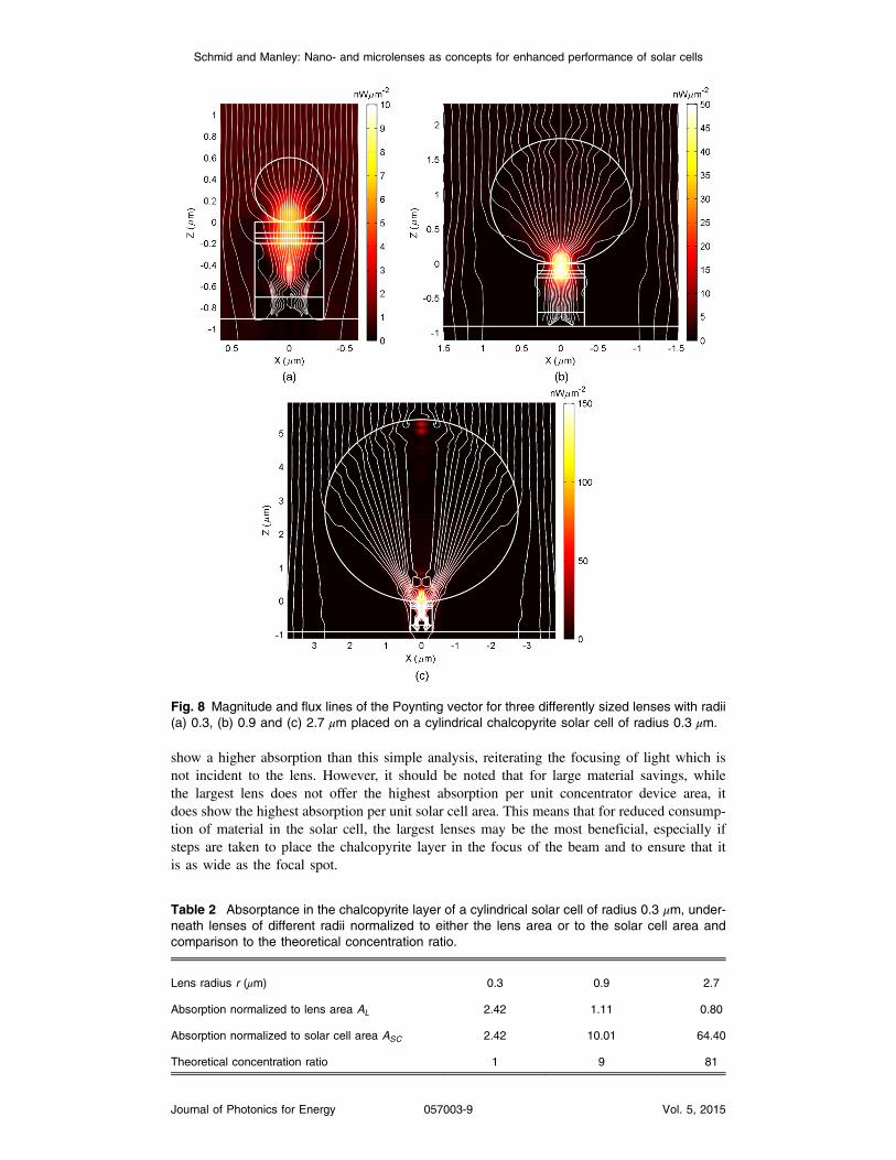
show a higher absorption than this simple analysis, reiterating the focusing of light which isnot incident to the lens. However, it should be noted that for large material savings, whilethe largest lens does not offer the highest absorption per unit concentrator device area, itdoes show the highest absorption per unit solar cell area. This means that for reduced consump-tion of material in the solar cell, the largest lenses may be the most beneficial, especially ifsteps are taken to place the chalcopyrite layer in the focus of the beam and to ensure that itis as wide as the focal spot.
Fig. 8 Magnitude and flux lines of the Poynting vector for three differently sized lenses with radii(a) 0.3, (b) 0.9 and (c) 2.7 μm placed on a cylindrical chalcopyrite solar cell of radius 0.3 μm.
Table 2 Absorptance in the chalcopyrite layer of a cylindrical solar cell of radius 0.3 μm, under-neath lenses of different radii normalized to either the lens area or to the solar cell area andcomparison to the theoretical concentration ratio.
Lens radius r (μm) 0.3 0.9 2.7
Absorption normalized to lens area AL 2.42 1.11 0.80
Absorption normalized to solar cell area ASC 2.42 10.01 64.40
Theoretical concentration ratio 1 9 81
Schmid and Manley: Nano- and microlenses as concepts for enhanced performance of solar cells
Journal of Photonics for Energy 057003-9 Vol. 5, 2015

5 Conclusions
From metallic nanospheres, we have made the link to lossless dielectric ones and taken a detailedlook at their focusing behavior particularly as a function of size. The 3-D optical simulationsusing the FEM reveal the strong local field enhancement in the shadow region behind the dielec-tric sphere and highlight the transition from near- to far-field focusing. The quantitative maps ofelectric field strength give insight into the local distribution of intensities including the area ofmaximum light concentration. For micrometer-sized spheres, this focusing area coincides withresults from ray tracing which give the value of the BFL itself. The results from ray tracing are inagreement with focal lengths calculated according to the geometrical optics and give us indi-cations of how the focal lengths can be tuned apart from adjusting the particle size. Both anincreased substrate refractive index and the transition from a spherical to a hemispherical orsegment-like shape can increase the focal length. For the particular application to solar cellswith the aim of a compact device design, a short distance of the point of highest intensityfrom the concentrating lens may be required. This brings us back to spherically shaped particlesof smaller sizes, which may win in terms of field enhancement in the close vicinity of the lens,and improve devices with very thin absorber layers. With respect to substantial material savingby horizontal reduction of the absorber size, however, microconcentrator solar cells may bebeneficial. They rely on microscaled lenses and can be promising when integrating adequatespacer layers in order to bring the microcells into the region of high field intensities.
Acknowledgments
The authors are grateful to the Helmholtz Association for support from the Initiative andNetworking Fund for the Young Investigator Group VH-NG-928.
References
1. K. R. Catchpole and A. Polman, “Plasmonic solar cells,” Opt. Express 16, 21793–21800(2008).
2. H. A. Atwater and A. Polman, “Plasmonics for improved photovoltaic devices,” Nat. Mater.9, 205–213 (2010).
3. S. Pillai et al., “Surface plasmon enhanced silicon solar cells,” J. Appl. Phys. 101, 093105(2007).
4. L. Fang et al., “Efficiency enhancement in organic solar cells with extended resonancespectrum of localized surface plasmon,” IEEE Photon. J. 5, 8400307 (2013).
5. M. Schmid et al., “Modeling plasmonic scattering combined with thin-film optics,”Nanotechnology 22, 025204 (2011).
6. J. Grandidier et al., “Light absorption enhancement in thin-film solar cells using whisperinggallery modes in dielectric nanospheres,” Adv. Mater. 23, 1272–1276 (2011).
7. C. R. Simovski et al., “Photovoltaic absorption enhancement in thin-film solar cells by non-resonant beam collimation by submicron dielectric particles,” J. Appl. Phys. 114, 103104(2013).
8. M. Schmid, P. Andrae, and P. Manley, “Plasmonic and photonic scattering and near fields ofnanoparticles,” Nanoscale Res. Lett. 9, 50 (2014).
9. Z. Chen, A. Taflove, and V. Backman, “Photonic nanojet enhancement of backscattering oflight by nanoparticles: a potential novel visible-light ultramicroscopy technique,” Opt.Express 12, 1214–1220 (2004).
10. S. Lee, L. Li, and Z. Wang, “Optical resonances in microsphere photonic nanojets,” J. Opt.16, 015704 (2014).
11. Y. E. Geints, E. K. Panina, and A. A. Zemlyanov, “Control over parameters of photonicnanojets of dielectric microspheres,” Opt. Commun. 283(23), 4775–4781 (2010).
12. J. Yoon et al., “Ultrathin silicon solar microcells for semitransparent, mechanically flexibleand microconcentrator module designs,” Nat. Mater. 7(11), 907–915 (2008).
13. M. Paire et al., “Toward microscale Cu(In,Ga)Se2 solar cells for efficient conversion andoptimized material usage: theoretical evaluation,” J. Appl. Phys. 108(3), 034907 (2010).
Schmid and Manley: Nano- and microlenses as concepts for enhanced performance of solar cells
Journal of Photonics for Energy 057003-10 Vol. 5, 2015

14. P. Perez-Higueras et al., “High concentrator photovoltaics efficiencies: present status andforecast,” Renewable Sustainable Energy Rev. 15, 1810–1815 (2011).
15. B. Reinhold et al., “Monolithically interconnected lameller Cu(In,Ga)Se2 micro solar cellsunder full white light concentration,” (2014), submitted for publication.
16. E. D. Palik, Handbook of Optical Constants of Solids, Academic Press, Orlando (1985).17. M. Bass et al. Handbook of Optics, Third Edition Volume IV: Optical Properties of
Materials, Nonlinear Optics, Quantum Optics, McGraw-Hill Education, NY (2009).18. J. Hoffmann et al., “Comparison of electromagnetic field solvers for the 3-D analysis of
plasmonic nano antennas,” Proc. SPIE 7390, 73900J (2009).19. www.jcmwave.com.20. S. Burger et al., “Finite-element simulations of light propagation through circular sub-
wavelength apertures,” Proc. SPIE 7366, 736621 (2009).21. www.zemax.com.22. M. Schmid and P. Manley, “Enhancing solar cell conversion efficiency by lenses on
the nano- and microscale,” Proc. SPIE 9178, 91780K (2014).23. M. Schmid et al., “Stability of plasmonic metal nanoparticles integrated in the back contact
of ultra-thin Cu(In,Ga)S2 solar cells,” Thin Solid Films 527, 308–313 (2013).24. C.-Y. Liu, “Ultra-high transmission of photonic nanojet induced modes in chains of core–
shell microcylinders,” Phys. Lett. A 376, 3261–3266 (2012).
Martina Schmid is a junior professor at the Freie Universität Berlin (FUB). She receivedher diploma in physics from the University of Augsburg in 2006, and her PhD fromFUB in 2010. Since 2012, she has been leading a Helmholtz Young Investigator Group on“Nanooptical Concepts for Chalcopyrite Solar Cells” at the Helmholtz-Zentrum Berlin. Hercurrent research interests include plasmonics and photonics for light management in ultra-thinsolar cells as well as concentration concepts for micrometer-sized solar cells.
Phillip Manley is a final-year PhD student at the Helmholtz Zentrum Berlin. He received hismaster’s degree in physics from the University of Durham in 2012. His current research interestsinclude simulation of novel concepts in plasmonics and photonics with a particular focus onphotovoltaics.
Schmid and Manley: Nano- and microlenses as concepts for enhanced performance of solar cells
Journal of Photonics for Energy 057003-11 Vol. 5, 2015